EP3523748B1 - Vibrationsförderersysteme für rfid-elemente - Google Patents
Vibrationsförderersysteme für rfid-elemente Download PDFInfo
- Publication number
- EP3523748B1 EP3523748B1 EP17791232.6A EP17791232A EP3523748B1 EP 3523748 B1 EP3523748 B1 EP 3523748B1 EP 17791232 A EP17791232 A EP 17791232A EP 3523748 B1 EP3523748 B1 EP 3523748B1
- Authority
- EP
- European Patent Office
- Prior art keywords
- rfid
- components
- component
- lead
- antenna
- Prior art date
- Legal status (The legal status is an assumption and is not a legal conclusion. Google has not performed a legal analysis and makes no representation as to the accuracy of the status listed.)
- Not-in-force
Links
Images



Classifications
-
- G—PHYSICS
- G06—COMPUTING OR CALCULATING; COUNTING
- G06K—GRAPHICAL DATA READING; PRESENTATION OF DATA; RECORD CARRIERS; HANDLING RECORD CARRIERS
- G06K19/00—Record carriers for use with machines and with at least a part designed to carry digital markings
- G06K19/06—Record carriers for use with machines and with at least a part designed to carry digital markings characterised by the kind of the digital marking, e.g. shape, nature, code
- G06K19/067—Record carriers with conductive marks, printed circuits or semiconductor circuit elements, e.g. credit or identity cards also with resonating or responding marks without active components
- G06K19/07—Record carriers with conductive marks, printed circuits or semiconductor circuit elements, e.g. credit or identity cards also with resonating or responding marks without active components with integrated circuit chips
- G06K19/077—Constructional details, e.g. mounting of circuits in the carrier
- G06K19/07718—Constructional details, e.g. mounting of circuits in the carrier the record carrier being manufactured in a continuous process, e.g. using endless rolls
-
- G—PHYSICS
- G06—COMPUTING OR CALCULATING; COUNTING
- G06K—GRAPHICAL DATA READING; PRESENTATION OF DATA; RECORD CARRIERS; HANDLING RECORD CARRIERS
- G06K7/00—Methods or arrangements for sensing record carriers, e.g. for reading patterns
- G06K7/10—Methods or arrangements for sensing record carriers, e.g. for reading patterns by electromagnetic radiation, e.g. optical sensing; by corpuscular radiation
- G06K7/10009—Methods or arrangements for sensing record carriers, e.g. for reading patterns by electromagnetic radiation, e.g. optical sensing; by corpuscular radiation sensing by radiation using wavelengths larger than 0.1 mm, e.g. radio-waves or microwaves
- G06K7/10366—Methods or arrangements for sensing record carriers, e.g. for reading patterns by electromagnetic radiation, e.g. optical sensing; by corpuscular radiation sensing by radiation using wavelengths larger than 0.1 mm, e.g. radio-waves or microwaves the interrogation device being adapted for miscellaneous applications
-
- B—PERFORMING OPERATIONS; TRANSPORTING
- B29—WORKING OF PLASTICS; WORKING OF SUBSTANCES IN A PLASTIC STATE IN GENERAL
- B29C—SHAPING OR JOINING OF PLASTICS; SHAPING OF MATERIAL IN A PLASTIC STATE, NOT OTHERWISE PROVIDED FOR; AFTER-TREATMENT OF THE SHAPED PRODUCTS, e.g. REPAIRING
- B29C65/00—Joining or sealing of preformed parts, e.g. welding of plastics materials; Apparatus therefor
- B29C65/48—Joining or sealing of preformed parts, e.g. welding of plastics materials; Apparatus therefor using adhesives, i.e. using supplementary joining material; solvent bonding
-
- B—PERFORMING OPERATIONS; TRANSPORTING
- B29—WORKING OF PLASTICS; WORKING OF SUBSTANCES IN A PLASTIC STATE IN GENERAL
- B29C—SHAPING OR JOINING OF PLASTICS; SHAPING OF MATERIAL IN A PLASTIC STATE, NOT OTHERWISE PROVIDED FOR; AFTER-TREATMENT OF THE SHAPED PRODUCTS, e.g. REPAIRING
- B29C65/00—Joining or sealing of preformed parts, e.g. welding of plastics materials; Apparatus therefor
- B29C65/56—Joining or sealing of preformed parts, e.g. welding of plastics materials; Apparatus therefor using mechanical means or mechanical connections, e.g. form-fits
- B29C65/64—Joining a non-plastics element to a plastics element, e.g. by force
-
- B—PERFORMING OPERATIONS; TRANSPORTING
- B31—MAKING ARTICLES OF PAPER, CARDBOARD OR MATERIAL WORKED IN A MANNER ANALOGOUS TO PAPER; WORKING PAPER, CARDBOARD OR MATERIAL WORKED IN A MANNER ANALOGOUS TO PAPER
- B31D—MAKING ARTICLES OF PAPER, CARDBOARD OR MATERIAL WORKED IN A MANNER ANALOGOUS TO PAPER, NOT PROVIDED FOR IN SUBCLASSES B31B OR B31C
- B31D1/00—Multiple-step processes for making flat articles ; Making flat articles
- B31D1/02—Multiple-step processes for making flat articles ; Making flat articles the articles being labels or tags
- B31D1/028—Applying RFID chips
-
- G—PHYSICS
- G06—COMPUTING OR CALCULATING; COUNTING
- G06K—GRAPHICAL DATA READING; PRESENTATION OF DATA; RECORD CARRIERS; HANDLING RECORD CARRIERS
- G06K19/00—Record carriers for use with machines and with at least a part designed to carry digital markings
- G06K19/02—Record carriers for use with machines and with at least a part designed to carry digital markings characterised by the selection of materials, e.g. to avoid wear during transport through the machine
- G06K19/025—Record carriers for use with machines and with at least a part designed to carry digital markings characterised by the selection of materials, e.g. to avoid wear during transport through the machine the material being flexible or adapted for folding, e.g. paper or paper-like materials used in luggage labels, identification tags, forms or identification documents carrying RFIDs
-
- G—PHYSICS
- G06—COMPUTING OR CALCULATING; COUNTING
- G06K—GRAPHICAL DATA READING; PRESENTATION OF DATA; RECORD CARRIERS; HANDLING RECORD CARRIERS
- G06K19/00—Record carriers for use with machines and with at least a part designed to carry digital markings
- G06K19/06—Record carriers for use with machines and with at least a part designed to carry digital markings characterised by the kind of the digital marking, e.g. shape, nature, code
- G06K19/067—Record carriers with conductive marks, printed circuits or semiconductor circuit elements, e.g. credit or identity cards also with resonating or responding marks without active components
- G06K19/07—Record carriers with conductive marks, printed circuits or semiconductor circuit elements, e.g. credit or identity cards also with resonating or responding marks without active components with integrated circuit chips
- G06K19/077—Constructional details, e.g. mounting of circuits in the carrier
- G06K19/07749—Constructional details, e.g. mounting of circuits in the carrier the record carrier being capable of non-contact communication, e.g. constructional details of the antenna of a non-contact smart card
-
- G—PHYSICS
- G06—COMPUTING OR CALCULATING; COUNTING
- G06K—GRAPHICAL DATA READING; PRESENTATION OF DATA; RECORD CARRIERS; HANDLING RECORD CARRIERS
- G06K19/00—Record carriers for use with machines and with at least a part designed to carry digital markings
- G06K19/06—Record carriers for use with machines and with at least a part designed to carry digital markings characterised by the kind of the digital marking, e.g. shape, nature, code
- G06K19/067—Record carriers with conductive marks, printed circuits or semiconductor circuit elements, e.g. credit or identity cards also with resonating or responding marks without active components
- G06K19/07—Record carriers with conductive marks, printed circuits or semiconductor circuit elements, e.g. credit or identity cards also with resonating or responding marks without active components with integrated circuit chips
- G06K19/077—Constructional details, e.g. mounting of circuits in the carrier
- G06K19/07749—Constructional details, e.g. mounting of circuits in the carrier the record carrier being capable of non-contact communication, e.g. constructional details of the antenna of a non-contact smart card
- G06K19/07773—Antenna details
- G06K19/07775—Antenna details the antenna being on-chip
-
- B—PERFORMING OPERATIONS; TRANSPORTING
- B29—WORKING OF PLASTICS; WORKING OF SUBSTANCES IN A PLASTIC STATE IN GENERAL
- B29L—INDEXING SCHEME ASSOCIATED WITH SUBCLASS B29C, RELATING TO PARTICULAR ARTICLES
- B29L2007/00—Flat articles, e.g. films or sheets
- B29L2007/004—Tags; Tickets
Definitions
- the present subject matter relates to manufacturing radio frequency identification (“RFID”) components that include an RFID element such as an RFID chip thereby assembled to another RFID component, such as an antenna.
- RFID radio frequency identification
- the subject matter includes handling and ordering of the RFID elements or chips and presenting same for assembly according to manufacturing systems and methods.
- RFID tags and labels are widely used to associate an object with an identification code.
- RFID devices generally have a combination of antennae and analog and/or digital electronics, which may include, for example, communications electronics, data memory, and control logic.
- RFID tags are used in conjunction with retail security systems, security locks in cars, for access control to buildings, and for tracking inventory and parcels.
- Various examples of RFID tags and labels are known in the art.
- RFID uses labels or "tags” that include electronic components that respond to radio frequency (“RC”) commands and signals to provide identification of each tag wirelessly.
- RFID tags and labels comprise an integrated circuit (“IC", or chip) attached to an antenna that responds to a reader using radio waves to store and access the information in the chip.
- RFID tags One of the obstacles to more widespread adoption of RFID technology is the cost of RFID tags and difficulties for optimization of economical manufacturing of RFID tags. Increased demand for RFID tags has manufacturers continuously seeking cost reduction and manufacturing simplification and speed.
- cost reduction and manufacturing simplification and speed One area for which cost reduction and manufacturing simplification and speed are sought concerns methods and systems for assembling components of RFID devices, such as assembling RFID elements or chips to an RFID antenna in an inexpensive and efficient manner, taking into consideration the propensity for damage to typical RFID elements or chips.
- Current methods typically provide RFID chips on substrates on single crystalline material, such as silicon wafers, which tend to be susceptible to chipping or damage. For example, a plurality of standard current silicon RFID chips are commonly provided on a wafer, to be placed on an antenna, interposer or other surface.
- Interposers typically include conductive leads or pads that are electrically coupled to the contact pads of the chips for coupling to the antennas.
- antennas will be assembled to or with these types of components.
- Examples of traditional assembly methods include removing RFID elements or chips from their wafer substrate by so called “flip chip” methods where the RFID element or chip is ejected from the wafer, picked up by a vacuum head, rotated (to achieve the flip), transferred to another vacuum head before being placed onto the desired component such as the antenna or interposer.
- Another traditional method is described as a "direct punch-down" by which the wafer is placed above the desired component such as antenna or interposer, and a pin pushes a chip out of the wafer down into the component for assembly such as antenna or interposer.
- US 2008/310938 A1 is reflected in the preamble of claim 1.
- vibratory feeders provide feed handling equipment for the manufacturing methods and systems of the present disclosure. Included in the disclosure is providing RFID chips formed on or of non-silicon substrates such as printed parts. These substrates are relatively flexible, of materials such as polymeric sheets or other plastics.
- vibratory feeders provide feed handling equipment for the manufacturing methods and systems of the present disclosure.
- RFID chips that are inherently flexible and with printed electronics, such as being made primarily from non-silicon organic or inorganic semiconductors, including polymers and metal oxide semiconductors. Some can be based on polythiophene, the polymer semiconductor, printed on a relatively flexible material such as polyester film. Others can utilize polymer semiconductors used for printing the circuitry.
- embodiments of a system and method of producing RFID components having an RFID chip or other element assembled with an antenna component, and RFID components thus produced are provided.
- Such embodiments include providing a plurality RFID components that are RFID elements (such as chips) that are inherently relatively flexible; placing the plurality of the RFID components into a vibratory feeder and allowing the vibratory feeder to orient the RFID components in at least one stream, the stream comprising a plurality of the RFID components, the leading one of which is a lead RFID component.
- a plurality of RFID antennas are on a movable support.
- the lead RFID component and one of the RFID antennas join together at a transfer station at which the lead RFID component combines with one of the RFID antennas to form a combined RFID component and antenna, which collects at a location downstream of the transfer station.
- a plurality of RFID devices can be formed.
- RFID components having an RFID chip or other element assembled with an antenna component, and RFID components thus produced.
- Such embodiments include providing a plurality RFID components that are RFID elements (such as chips) that are inherently relatively flexible; placing the plurality of the RFID components into a vibratory feeder and allowing the vibratory feeder to orient the RFID components in at least one stream, the stream comprising a plurality of the RFID components, the leading one of which is a lead RFID component.
- a plurality of RFID antennas are on a movable support that follows a move and stop pattern.
- the lead RFID component and one of the RFID antennas enter a transfer station, the movable support stops, and the lead RFID component engages one of the RFID antennas to form a combined RFID component and antenna, which collects at a location downstream of the transfer station.
- a plurality of RFID devices can be formed.
- the lead RFID component and one of the RFID antennas enter a transfer station, the movable support stops, a pusher engages the lead RFID component into engagement with one of the RFID antennas to form a combined RFID component and antenna, which collects at a location downstream of the transfer station.
- a plurality of RFID devices can be formed.
- Added aspects or embodiments concern a system and method of producing RFID components having an RFID chip or other element assembled with an antenna component, and RFID components thus produced.
- Such embodiments include providing a plurality RFID components that are RFID elements (such as chips) that are inherently relatively flexible; placing the plurality of the RFID components into a vibratory feeder and allowing the vibratory feeder to orient the RFID components in at least one stream, the stream comprising a plurality of the RFID components, the leading one of which is a lead RFID component.
- a plurality of RFID antennas are on a movable support that follows a continuous flow pattern.
- the lead RFID component and one of the RFID antennas enter a transfer station, a pusher engages and moves with the RFID component in response to movement of the movable support, with the lead RFID component engaging one of the RFID antennas to form a combined RFID component and antenna, which collect at a location downstream of the transfer station.
- a plurality of RFID devices can be formed.
- embodiments concern a system and method of producing RFID components having an RFID chip or other element assembled with an antenna component, and RFID components thus produced.
- Such embodiments include providing a plurality RFID components that are RFID elements (such as chips) that are inherently relatively flexible; placing the plurality of the RFID components into a vibratory feeder and allowing the vibratory feeder to orient the RFID components in at least one stream, the stream comprising a plurality of the RFID components, the leading one of which is a lead RFID component.
- a plurality of RFID antennas are on a movable support.
- a vacuum cylinder mechanism is operatively positioned between the stream of RFID components and the movable support and receives each lead RFID component from their stream and moves same to a transfer station, typically while timing delivery of the RFID components to the transfer station to coordinate closely with the phase and timing of delivery of the RFID antennas to the transfer station.
- the RFID components and the RFID antennas combine to form a series of combined RFID components and antennas, which collect at a location downstream of the transfer station.
- a vacuum cylinder mechanism is operatively positioned between the stream of RFID components and the movable support and receives each lead RFID component from their stream in serial fashion, with the vacuum cylinder mechanism spacing the plurality of RFID components at a distance that correlates with spacing between the plurality of RFID antennas in ordered sequence on the movable support and to the transfer station to coordinate closely with the phase and timing of delivery of the RFID antennas to the transfer station.
- the RFID components and the RFID antennas combine to form a series of combined RFID components and antennas, which collect at a location downstream of the transfer station.
- Another aspect and embodiments of a system and method of producing RFID components having an RFID chip or other element assembled with an antenna component, and RFID components thus produced, are provided.
- Such embodiments include providing a plurality RFID components that are RFID elements (such as chips) that are inherently relatively flexible; placing the plurality of the RFID components into a vibratory feeder and allowing the vibratory feeder to orient the RFID components in at least one stream, the stream comprising a plurality of the RFID components, the leading one of which is a lead RFID component.
- a plurality of RFID antennas are on a movable support.
- the lead RFID component and one of the RFID antennas join together at a transfer station at which the lead RFID component combines with one of the RFID antennas in conjunction with a securement feature that includes adhesives, conductive adhesives, dielectric adhesives, pressure sensitive adhesives, epoxy adhesives, anisotropic conductive paste, heat sensitive adhesives, heat and pressure sensitive adhesives, hot melt adhesives, welding, ultrasonic welding, electronic welding, magnet field systems, electronic field systems, and combinations thereof.
- a securement feature that includes adhesives, conductive adhesives, dielectric adhesives, pressure sensitive adhesives, epoxy adhesives, anisotropic conductive paste, heat sensitive adhesives, heat and pressure sensitive adhesives, hot melt adhesives, welding, ultrasonic welding, electronic welding, magnet field systems, electronic field systems, and combinations thereof.
- embodiments of a system and method of producing RFID components having an RFID chip or other element assembled with an antenna component, and RFID components thus produced are provided.
- Such embodiments include providing a plurality of RFID components that are RFID elements (such as chips) that are inherently relatively flexible. These RFID components exhibit an orientation feature as the RFID components vibrate in a vibratory feeder and allowing the vibratory feeder to orient the RFID components in at least one stream, the stream comprising a plurality of the RFID components, the leading one of which is a lead RFID component.
- a plurality of RFID antennas are on a movable support.
- the lead RFID component and one of the RFID antennas join together at a transfer station at which the lead RFID component combines with one of the RFID antennas to form a combined RFID component and antenna, which collects at a location downstream of the transfer station.
- the orientation feature enhances orientation of the RFID components with respect to the RFID antennas for the combined RFID components and antennas, the orientation feature being a vision system, providing the RFID components with surface characteristics of opposing faces different from each other, providing the RFID components with differently shaped opposing faces, providing the RFID components with opposing faces with identical operative features for joining with the RFID antennas, or combinations thereof
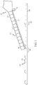
- a vibratory feeder is generally indicated at 21 in Fig. 1 .
- This feeder 21 is provided for the purpose of receiving RFID elements 22 such as chips, herein variously referred to as RFID components, in a non-ordered or random fashion typically by dumping a plurality of such RFID elements into the bowl of the vibratory feeder 21.
- the vibratory feeder 21 the RFID components 22 ride on an acoustic wave and achieve "singulation" of the initially randomized plurality of RFID elements, resulting in a stream 23 of the singulated RFID components or elements that flows along a support 24 such as an exit ramp of the vibratory feeder.
- the stream provides a series of lead RFID element or chip components 25 as the RFID elements move along, typically in a downward direction, the support 24.
- Each newly presented lead RFID element or component 25 exits the ramp to the next phase of the system, to be immediately replaced by the next chip in the stream that becomes the current transient lead RFID element or chip component 25.
- vibratory feeders are well known and used in various levels of manufacturing and product handling, in order to take parts in a random orientation in a bowl or the like and create a stream of single items to be delivered in a controlled manner, usually one at a time.
- the overall operation of a vibratory feeder can be described as a "singulation" of random parts or components to allow for single-part presentation to a manufacturing or processing operation. It will be understood that the action of vibratory feeders causes the parts in the bowl to engage each other with relative motion of the parts that is best suited to parts that will not be damaged by such relative motion and engagement, as well as the energy applied to the bowl to achieve rapid vibration and relative movement of the parts.
- RFID elements or chips being made primarily of silicon, are damaged by the forces applied to the elements or chips by such relative motion and vibratory action. Such forces tend to cause chipping and other damage to RFID element or chip components.
- the present disclosure modifies or substitutes for typical RFID elements or chips to provide the RFID elements 22 such as chips which are dumped into the vibratory feeder bowl, singulated into the stream 23 are presented as the lead RFID element or chip component 25, and secured to the RFID antennas 27.
- the vibratory feeder system is adapted to non-silicon chips such as printed parts, which can withstand impacts, allowing the RFID element or chip components 22 to be released from a wafer all at once and dropped into the feed hopper for vibratory feed action and singulation without damage to the RFID element or chip components 22.
- the RFID element or chip components are formed on or of relatively flexible substrates such as plastics. Typical plastics include polymers and non-hydrocarbon plastics. Due to the nature of these components, they are very resistant to damage caused by contact with other chips in the bowl feeder.
- RFID element or chip components 22 include ones that are inherently flexible and with printed electronics, such as being made primarily from non-silicon organic or inorganic semiconductors, including polymers and metal oxide semiconductors. Some can be based on polythiophene, the polymer semiconductor, printed on a relatively flexible material such as polyester film. Other polymer semiconductors could be used for printing the circuitry as desired.
- each RFID antenna 27 includes a securement feature such as a coating on its upper surface for facilitating securement of an RFID element or chip component 22 to the antenna 27, examples including adhesives such as pressure sensitive adhesives, heat sensitive adhesives, pressure and heat sensitive adhesives, anaerobic adhesives, epoxy adhesives such as conductive epoxy.
- adhesives such as pressure sensitive adhesives, heat sensitive adhesives, pressure and heat sensitive adhesives, anaerobic adhesives, epoxy adhesives such as conductive epoxy.
- the lead RFID element or chip component 25 is ejected onto the RFID antenna 27 into or onto an adhesive, and pressure and heat is applied to complete the bond, such being supplied by a moving web or belt downstream of a transfer station 28. Whatever mechanism or material is used, the result is securement of the RFID antenna to the RFID element or chip component.
- RFID antennas and/or RFID element or chip components typically to enhance attachment capabilities and/or improve functionality.
- These can take the form of interposers, pads and the like.
- RFID antennas or chips and particularly of RFID antennas, it will be understood that any such reference is not intended to exclude these types of components.
- RFID antennas it will be understood to include RFID antennas with or without interposers, pads or the like and/or to assembly at or not at an interposer, pad or the like rather than directly to the antenna material.
- the lead RFID element or chip component 22 and RFID antenna 27 meet at the transfer station 28 at which location these components engage each other and activate the securement action resulting in combining these parts into and form an RFID device 29 with functionality for a passive RFID application.
- the web 26 follows a move and stop flow pattern. Suitable controls such as those known in the art time operation of the web 26 with the presentation of a lead RFID element or chip whereby the antenna and chip reach the transfer station 28 at essentially the same time for initiating the securement action by which the RFID device 29 is formed.
- the web 26 translates in a linear direction of motion as illustrated by the arrow marking 30 on Fig. 1 through the use of a suitable translating mechanism available in the art. Mechanical support for lateral movement or translation and stopping of the web typically is provided in accordance with machinery, devices, structures and/or materials known in the art such as conveying systems.
- This linear direction translation of the web stops when an RFID antenna reaches the transfer station, at which time the lead RFID element or chip component 25 is deposited on and engages the RFID antenna that is at the station at that time.
- the web is stationary with respect to the element or chip at the time of ejection of the lead RFID element or chip component 25. Thereafter, the web movement continues, with the RFID devices 29 moving downstream of the transfer station. When desired, completion of the securement action can take place once the combined units move to another processing station downstream of the transfer station.
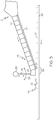
- Fig. 2 shows an embodiment that is a variation on the approaches illustrated in Fig. 1 .
- This incorporated the move and stop system of the web 26 for receiving the lead RFID element or chip component 25 where securement action in initiated.
- This Fig. 2 embodiment adds features whereby the lead RFID element or chip component 25 is pushed down onto the web by a pin or pusher 31 positioned above a transfer station 28a.
- This pin or pusher asserts a downward force on the lead RFID element or chip component 25 to apply pressure in assisting with securement action for joining together the RFID element or chip component and the RFID antenna 27 to form the RFID device 29.
- this approach modifies an embodiment of the approaches illustrated by Fig. 2 .
- a continuous-motion web 36 is provided.
- web 36 continues to flow without having to stop to load the feed RFID element or chip component 25 onto the RFID antenna 27 at transfer station 38.
- a line of RFID antennas 27 are positioned along the web 36, being spaced according to the timing set for synchronizing the system.
- a pin or pusher 32 is provided that is modified from pin or pusher 31 of Fig. 2 , which moves essentially along a linear (typically vertical) path.
- a pivot mechanism 33 is associated with pin or pusher 32 whereby the pin or pusher 32 is able to follow movement of the RFID antenna 27 while within the transfer station 38. In doing so, the pin or pusher 32 follows a swinging motion as illustrated at 39 in Fig. 3 allowing the lead RFID element or chip component 25 to accelerate until it moves at a speed that matches the motion speed of the continuous flow web 36, thereby allowing the web 36 to move continuously.
- FIG. 4 A further alternative embodiment for effecting well-timed engagement between RFID chip flow and antenna flow is illustrated in Fig. 4 .
- This embodiment also incorporates a continuous-flow web 46, while positioning a vacuum cylinder mechanism 41 that rotates along an axis 42 in a counter-clockwise direction as viewed in Fig. 4 .
- the vibratory feeder 21 receives a plurality of RFID element or chip components 22, singulates them into the stream 23, and presents a series of lead RFID element or chip components 25.
- the vacuum application locates the element or chip component on the outer cylindrical surface of the rotating vacuum cylinder mechanism 41.
- This interaction effects acceleration such that the element or chip component 22a on the vacuum cylinder mechanism 41 has a radial velocity or rotational speed that correlates with the linear speed of the continuous-flow web 46 and at the desired pitch to coordinate with the desired pitch on the web 46.
- the desired pitch corresponds to the pitch of the series of antennas on the web 46.
- This action can include having the vacuum cylinder accelerate to the chip to match web speed at the desired pitch for web contact, accept the chip ejected onto the cylinder, and achieve the radial velocity or rotational speed that accurately coordinates with the desired pitch.
- the arrow path 44 between component 22a and component 22b along the cylindrical face of the vacuum cylinder 41 correlates to the antenna pitch on the web 46.
- the radial velocity of the vacuum cylinder 41 matches the web speed, or may correlate to the web speed so the overall system is properly synchronized. Proper synchronization allows for consistent accurate placement of an RFID component 22c at the transfer station 48 to achieve proper alignment of RFID component 22c with the RFID antenna 47 and ultimate assembly of the RFID device 49.
- the Fig. 5 embodiment features pulling the lead RFID component 25 from the dispenser or stream 23 of RFID components 22 on the support 24 leading out of the vibrating feeder 21. This pulling out or pulling from the dispenser is initiated by engagement with a component on the moving web 56.
- a component on the moving web 56 can be an RFID antenna 57 that drags the lead RFID element or chip 25 away from the dispenser or stream as the antenna moves through the transfer section 58.
- RFID antenna 57 typically will include a securement feature for initiating dislodgement of the lead RFID element or chip 25 and maintenance of connection between chip and antenna. Securement features in this regard include adhesives, including same with sufficient tack to achieve a desired result and eventual securement of chip and antenna into RFID devices 59, as well as other securement features including securement elements and approaches noted herein.
- the web 56 can continue to move and move at a constant velocity, with the constant velocity enhancing the ability of the antenna component to engage and "drag" the lead RFID element or chip component.
- the element or chip component is pulled from the dispenser by the antenna (with or without interposer or other components as discussed herein) at the position it needs to be attached by a surface feature engaging with the chip edge.
- the RFID devices 29, 49, 59 are finished RFID devices in that they including traditional basis components of RFID element or chip and RFID antenna. Same can be further modified as desired, in which case, the devices 29, 49, 59 form what might be considered intermediate components in making desired complete RFID products such as tags and the like.
- These embodiments create antenna components in a system of creating RFID components added at a later stage to manufacture the final RFID device. This is a typical approach for manufacturing RFID tags, and the antenna component is coupled to the RFID element at a later stage, on the same line or a separate line.
- the securement feature can be achieved in various manners including use of securement elements and approaches. Included are the following. If the surface area of engagement surfaces on the RFID element or chip component 22 (for example pads) are large enough, securement may occur via capacitance through a dielectric adhesive such as a pressure sensitive adhesive. Use an epoxy adhesive, such as an anisotropic conductive paste that contains particles to facilitate a good joint when the RFID element or chip 22 is compressed against the bond pads and heat is applied. These bond pads can be on the RFID antenna.
- Coat a front surface of the RFID element or chip 22 with an adhesive during its manufacturing process examples of adhesives being hot melt adhesives, including heating either or both of the element or chip 22, or of the web or cylinder prior to and/or during assembly and securement.
- adhesives being hot melt adhesives, including heating either or both of the element or chip 22, or of the web or cylinder prior to and/or during assembly and securement.
- Weld using ultrasonic methods where the flexibility of the RFID element or chip 22 and the ability to tune the thickness and the drive frequency to achieve maximum effect, such as resonance.
- Weld using electrical methods where side contacts connecting to the front contacts formed on the RFID element or chip component 22 allow a welding voltage to be applied without needing access to the front furnace during the process.
- the RFID element or chip components and/or RFID antennas may have a coupling structure such as magnetic loops and/or pads attached. Coupling or securement between the RFID antennas and the RFID element or chip loops, pads or other coupling structures or interposers can be by magnetic fields, by electric fields, by a combination of both magnetic and electric fields, or by a conductive connection using a conductive adhesive. Alternatively, the RFID antennas can be welded to the RFID elements or chips.
- RFID chips are symmetrical with the result they can leave the vibratory feeder either face up, and one of the faces is designed for working relationship with the RFID antenna, while the other side is not so designed. Accordingly, without further modification, RFID chips will leave the vibratory feeder and form a stream of chips, some "right side up” and some "upside down".
- One solution to this problem is to include a monitor (61 in Fig. 1 ) such as a vision system that identifies chips positioned at the wrong orientation and ejects them back into the bowl after or before they enter the stream, through a suitable return mechanism (not shown).
- a monitor such as a vision system that identifies chips positioned at the wrong orientation and ejects them back into the bowl after or before they enter the stream, through a suitable return mechanism (not shown).
- Another solution modifies the chips themselves to present a mechanical surface on one face that is different from the mechanical surface of the other face. In one embodiment of this type, one surface is smooth and the other is rough, which allows the bowl vibration processing to pick up for movement to the stream only chips that feature the surface that presents the desired orientation of the chip.
- a further embodiment of this type may be shaped in which can be considered to be "3D"; for example, a flat side on one face and a curved side on the opposite face, and chips with a curved side will tend to fall back into the bowl as they do not engage with the feeder spiral in a stable fashion.
- a further solution is to manufacture the RFID elements or chips 22 in a way that orientation is not important; for example, each of the top and bottom face has identical components, including identical contacts for engagement with the RFID antenna.
- this mechanism and system allows for flexible manufacture of RFID devices according to different approaches for engaging components with each other and securing them together into RFID devices.
- the method and system achieve these advantageous results with significantly lower capital expenditure due to the relative lack of expense of equipment in the nature of vibrating feeders that can be used advantageously for handling and singulating RFID elements or chips without damaging same.
- the movements and/or start and stop movements of the webs described herein are capable of being controlled by suitable movement generators and controllers.
- software can be incorporated in a suitable control system that allows the operator to select among numerous combinations of web flow speed and production line output. It is possible to vary such parameters as desired and to provide a flow of and engagement of components to form the RFID devices according to the selected configurations and parameters.
Landscapes
- Engineering & Computer Science (AREA)
- Physics & Mathematics (AREA)
- General Physics & Mathematics (AREA)
- Theoretical Computer Science (AREA)
- Toxicology (AREA)
- Health & Medical Sciences (AREA)
- Microelectronics & Electronic Packaging (AREA)
- Computer Hardware Design (AREA)
- Mechanical Engineering (AREA)
- Computer Vision & Pattern Recognition (AREA)
- Artificial Intelligence (AREA)
- General Health & Medical Sciences (AREA)
- Electromagnetism (AREA)
- Computer Networks & Wireless Communication (AREA)
- Supply And Installment Of Electrical Components (AREA)
- Details Of Aerials (AREA)
Claims (12)
- System zur Herstellung von RFID-Vorrichtungen (29), umfassend:eine Vielzahl von RFID-Komponenten (22, 25), wobei die RFID-Komponenten (22, 25) RFID-Elemente oder -Chips sind, die in sich flexibel sind;einen Vibrationsförderer (21), der die Vielzahl von RFID-Komponenten (22, 25) enthält, wobei der Vibrationsförderer (21) die RFID-Komponenten (22, 25) bewegt und ausrichtet, und die RFID-Komponenten (22, 25) in mindestens einem Strom (23) von RFID-Komponenten (22, 25) ausgibt, wobei der Strom (23) eine Vielzahl der RFID-Komponenten (22, 25) umfasst, wobei die führende von ihnen als eine Führungs-RFID-Komponente (25) definiert ist;eine vorgelagerte bewegliche Stütze, die einer Übergabestation (28) vorgelagert angeordnet ist, und eine Vielzahl von RFID-Antennen (27) in einer geordneten Reihenfolge auf der vorgelagerten beweglichen Stütze;wobei die Übergabestation (28) eine Stelle bereitstellt, an der die Führungs-RFID-Komponente (25) mit einer der RFID-Antennen (27) in Eingriff tritt, wenn sie die Übergabestation (28) erreicht, wodurch eine kombinierte RFID-Komponente (22, 25) und Antenne (27) zusammengesetzt wird; undeine nachgelagerte Stütze, die der Übergabestation (28) nachgelagert angeordnet ist, wobei die nachgelagerte Stütze die kombinierte RFID-Komponente (22, 25) und Antenne (27) zur Herstellung der RFID-Vorrichtung (29) sammelt;wobei die vorgelagerte bewegliche Stütze und die nachgelagerte Stütze eine einstückige bewegliche Stütze umfassen, die die Übergabestation (28) durchquert, wobei die einstückige Stütze eine Bahn (26) in kontinuierlicher Bewegung ist, dadurch gekennzeichnet, dass sie ferner einen schwenkbaren Schieber (31) an der Übergabestation (28) umfasst, der eine im Allgemeinen nach unten gerichtete Kraft auf die Führungs-RFID-Komponente (25) ausübt, um die Bildung der kombinierten RFID-Komponente (22, 25) und Antenne (27) zu unterstützen, und wobeider schwenkbare Schieber (31) einen fernen Endabschnitt aufweist, der Bewegungen der Bahn (26) in kontinuierlicher Bewegung folgt, während er die nach unten gerichtete Kraft auf die Führungs-RFID-Komponente (25) ausübt.
- System nach Anspruch 1, ferner umfassend einen Vakuumzylindermechanismus (41), der operativ zwischen dem Strom (23) von RFID-Komponenten (22, 25) und der Übergabestation (28) angeordnet ist, wobei der Vakuumzylindermechanismus (41) die Führungs-RFID-Komponente (25) aus dem Strom (23) von RFID-Komponenten (22, 25) empfängt, wobei die vorgelagerte bewegliche Stütze und die nachgelagerte Stütze eine bewegliche Stütze umfassen, die eine ausgewählte lineare Bewegungsgeschwindigkeit aufweist, wobei der Vakuumzylindermechanismus (41) der Führungs-RFID-Komponente (25) eine Radialgeschwindigkeit verleiht, die mit der linearen Geschwindigkeit der beweglichen Stütze korreliert und die Führungs-RFID-Komponente (25) auf dem Vakuumzylindermechanismus (41) beabstandet, wodurch die Führungs-RFID-Komponente (25) sich an der Übergabestation (28) von dem Vakuumzylindermechanismus (41) auf eine RFID-Antenne (22, 25) ablagert, um die kombinierte RFID-Komponente (22, 25) und Antenne (27) zu bilden.
- System nach Anspruch 2, wobei der Vakuumzylindermechanismus (41) aus dem Strom (23) nacheinander eine Vielzahl von Führungs-RFID-Komponenten (25) empfängt, und der Vakuumzylindermechanismus (41) die Vielzahl von Führungs -RFID-Komponenten (25) in einem Abstand beabstandet, der mit den Abständen zwischen der Vielzahl von RFID-Antennen (22, 25) in geordneter Reihenfolge auf der vorgelagerten beweglichen Stütze korreliert.
- System nach Anspruch 3, wobei die bewegliche Stütze eine Bahn (26) in kontinuierlicher Bewegung ist.
- System nach Anspruch 1, wobei die RFID-Antennen (22, 25) ein Sicherungsmerkmal umfassen, wobei die vorgelagerte bewegliche Stütze und die nachgelagerte Stütze eine einstückige bewegliche Stütze umfassen, die die Übergabestation (28) durchquert, wobei die einstückige Stütze eine Bahn (26) in kontinuierlicher Bewegung ist, die der Übergabestation (28) eine beabstandete Reihe von RFID-Antennen (27) mit Sicherungsmerkmal präsentiert, wo das Sicherungsmerkmal der einzelnen RFID-Antennen (27) der beabstandeten Reihe die RFID-Komponente (25) aus dem Strom (23) von RFID-Komponenten (22, 25) zieht, um die kombinierte RFID-Komponente (22, 25) und Antenne (27) zu bilden.
- System nach Anspruch 5, wobei das Sicherungsmerkmal ausgewählt ist aus der Gruppe bestehend aus Klebstoffen, leitfähigen Klebstoffen, dielektrischen Klebstoffen, Haftklebstoffen, Epoxidklebstoffen, anisotroper leitfähiger Paste, wärmeempfindlichen Klebstoffen, wärme- und druckempfindlichen Klebstoffen, Schmelzklebstoffen, Schweißen, Ultraschallschweißen, Elektroschweißen, Magnetfeldsystemen, elektrischen Feldsystemen und Kombinationen davon.
- System nach Anspruch 1, wobei die RFID-Komponente (22, 25), die RFID-Antenne oder beide ein Sicherungsmerkmal aufweisen, das ausgewählt ist aus der Gruppe bestehend aus Klebstoffen, leitfähigen Klebstoffen, dielektrischen Klebstoffen, Haftklebstoffen, Epoxidklebstoffen, anisotroper leitfähiger Paste, wärmeempfindlichen Klebstoffen, wärme- und druckempfindlichen Klebstoffen, Schmelzklebstoffen, Schweißen, Ultraschallschweißen, Elektroschweißen, Magnetfeldsystemen, elektrischen Feldsystemen und Kombinationen davon.
- System nach Anspruch 1, wobei die RFID-Komponenten (22, 25), die in sich flexibel sind, Nicht-Silizium-Chips aus flexiblem Kunststoffinaterial mit gedruckter Elektronik sind.
- System nach Anspruch 1, wobei die RFID-Komponenten (22, 25) ein Ausrichtungsmerkmal umfassen, während die RFID-Komponenten (22, 25) in dem Vibrationsförderer (21) vibrieren, wobei das Ausrichtungsmerkmal die Ausrichtung der RFID-Komponenten (22, 25) in Bezug auf die RFID-Antennen (27) für die kombinierten RFID-Komponenten (22, 25) und Antennen (27) verbessert, wobei das Ausrichtungsmerkmal ausgewählt ist aus der Gruppe bestehend aus Überwachen mit einem Bildverarbeitungssystem, Versehen der RFID-Komponenten (22, 25) mit Oberflächeneigenschaften von gegenüberliegenden Seiten, die sich voneinander unterscheiden, Versehen der RFID-Komponenten (22, 25) mit unterschiedlich geformten gegenüberliegenden Seiten, Versehen der RFID-Komponenten (22, 25) mit gegenüberliegenden Seiten mit identischen operativen Merkmalen zur Verbindung mit den RFID-Antennen (27) und Kombinationen davon.
- Verfahren zur Herstellung von RFID-Vorrichtungen (29), umfassend:Bereitstellen einer Vielzahl von RFID-Komponenten (22, 25), wobei die RFID-Komponenten (22, 25) RFID-Elemente oder -Chips sind, die in sich flexibel sind;Ablagern der Vielzahl von RFID-Komponenten (22, 25) in einer Schale eines Vibrationsförderers (21) und Bewegen und Ausrichten der RFID-Komponenten (22, 25) in der Schale des Vibrationsförderers;Ausgeben der RFID-Komponenten (22, 25) in mindestens einem Strom (23) von RFID-Komponenten (22, 25), wobei der Strom (23) eine Vielzahl der RFID-Komponenten (22, 25) umfasst, wobei die führende von ihnen als eine Führungs-RFID-Komponente (25) definiert ist;Bereitstellen einer beweglichen Stütze, die eine Vielzahl von RFID-Antennen (27) in einer geordneten Reihenfolge auf der beweglichen Stütze aufweist, wobei die bewegliche Stütze daran entlang eine Übergabestation (28) aufweist;wobei die bewegliche Stütze eine Bahn (26) in kontinuierlicher Bewegung ist, die an der Übergabestation (28) einen Schieber (31) schwenkt und durch den Schieber (31) eine im Allgemeinen nach unten gerichtete Kraft auf die Führungs-RFID-Komponente (25) ausübt und die Bildung der kombinierten RFID-Komponente (22, 25) und Antenne (27) unterstützt, ferner umfassend das Schwenken des Schiebers (31) und Bewegen eines fernen Endabschnitts davon, der Bewegungen der Bahn (26) in kontinuierlicher Bewegung folgt, während er die nach unten gerichtete Kraft auf die Führungs-RFID-Komponente (25) ausübt;Ineingriffbringen, während sie sich an der Übergabestation (28) befindet, der Führungs-RFID-Komponente (25) mit einer der RFID-Antennen (27) und Zusammensetzen derselben zu einer kombinierten RFID-Komponente (22, 25) und Antenne (27); undSammeln der kombinierten RFID-Komponente (22, 25) und Antenne (27) und Bereitstellen einer RFID-Vorrichtung (29) daraus.
- Verfahren nach Anspruch 10, ferner umfassend das operative Anordnen eines Vakuumzylindermechanismus (41) zwischen dem Strom (23) von RFID-Komponenten (22, 28) und der Übergabestation (28), Empfangen der Führungs-RFID-Komponente (25) aus dem Strom (23) von RFID-Komponenten (22, 25) an dem Vakuumzylindermechanismus (41), Bewegen der beweglichen Stütze mit einer ausgewählten linearen Bewegungsgeschwindigkeit, Verleihen einer Radialgeschwindigkeit an die Führungs-RFID-Komponente (25) durch den Vakuumzylindermechanismus (41), die mit der linearen Geschwindigkeit der beweglichen Stütze korreliert und die Führungs-RFID-Komponente (25) auf dem Vakuumzylindermechanismus (41) beabstandet, und Ablagern der Führungs-RFID-Komponente (25) von dem Vakuumzylindermechanismus (41) auf eine RFID-Antenne (27) an der Übergabestation (28), um die kombinierte RFID-Komponente (22, 25) und Antenne (27) zu bilden.
- Verfahren nach Anspruch 10, ferner umfassend das Ausrichten der RFID-Komponenten (22, 25), während die RFID-Komponenten (22, 25) in dem Vibrationsförderer (21) vibrieren, wobei das Ausrichten die Ausrichtung der RFID-Komponenten (22, 25) in Bezug auf die RFID-Antennen (27) für das Ineingriffbringen zum Bilden der kombinierten RFID-Komponenten (22, 25) und Antennen (27) verbessert, wobei das Ausrichten ausgewählt ist aus der Gruppe bestehend aus Überwachen mit einem Bildverarbeitungssystem, Versehen der RFID-Komponenten (22, 25) mit Oberflächeneigenschaften von gegenüberliegenden Seiten, die sich voneinander unterscheiden, Versehen der RFID-Komponenten (22, 25) mit unterschiedlich geformten gegenüberliegenden Seiten, Versehen der RFID-Komponenten (22, 25) mit gegenüberliegenden Seiten mit identischen operativen Merkmalen zur Verbindung mit den RFID-Antennen (27) und Kombinationen davon.
Applications Claiming Priority (2)
| Application Number | Priority Date | Filing Date | Title |
|---|---|---|---|
| US15/288,212 US10685273B2 (en) | 2016-10-07 | 2016-10-07 | Vibratory feeder systems for RFID elements |
| PCT/US2017/055532 WO2018067927A1 (en) | 2016-10-07 | 2017-10-06 | Vibratory feeder systems for rfid elements |
Publications (2)
| Publication Number | Publication Date |
|---|---|
| EP3523748A1 EP3523748A1 (de) | 2019-08-14 |
| EP3523748B1 true EP3523748B1 (de) | 2021-03-03 |
Family
ID=60186379
Family Applications (1)
| Application Number | Title | Priority Date | Filing Date |
|---|---|---|---|
| EP17791232.6A Not-in-force EP3523748B1 (de) | 2016-10-07 | 2017-10-06 | Vibrationsförderersysteme für rfid-elemente |
Country Status (4)
| Country | Link |
|---|---|
| US (1) | US10685273B2 (de) |
| EP (1) | EP3523748B1 (de) |
| CN (1) | CN109997145A (de) |
| WO (1) | WO2018067927A1 (de) |
Cited By (1)
| Publication number | Priority date | Publication date | Assignee | Title |
|---|---|---|---|---|
| RU206701U1 (ru) * | 2021-06-22 | 2021-09-22 | ОБЩЕСТВО с ОГРАНИЧЕННОЙ ОТВЕТСТВЕННОСТЬЮ "Стромизмеритель" | Двухсекционный вибрационный питатель стеклобоя |
Families Citing this family (9)
| Publication number | Priority date | Publication date | Assignee | Title |
|---|---|---|---|---|
| CN111386170A (zh) | 2017-11-29 | 2020-07-07 | 远程声波控股公司 | 超声加工设备、超声加工设备的配置方法及具有这种超声加工设备的系统 |
| WO2019224575A1 (en) | 2018-05-22 | 2019-11-28 | Tyco Fire & Security Gmbh | Elongate flexible tag |
| US12223814B2 (en) | 2019-09-16 | 2025-02-11 | Sensormatic Electronics, LLC | Security tag for textiles using conductive thread |
| US11443160B2 (en) | 2019-09-18 | 2022-09-13 | Sensormatic Electronics, LLC | Systems and methods for laser tuning and attaching RFID tags to products |
| US10970613B1 (en) | 2019-09-18 | 2021-04-06 | Sensormatic Electronics, LLC | Systems and methods for providing tags adapted to be incorporated with or in items |
| US11055588B2 (en) | 2019-11-27 | 2021-07-06 | Sensormatic Electronics, LLC | Flexible water-resistant sensor tag |
| US12524640B2 (en) | 2019-11-27 | 2026-01-13 | Sensormatic Electronics, LLC | Flexible water-resistant sensor tag |
| US11755874B2 (en) | 2021-03-03 | 2023-09-12 | Sensormatic Electronics, LLC | Methods and systems for heat applied sensor tag |
| US11869324B2 (en) | 2021-12-23 | 2024-01-09 | Sensormatic Electronics, LLC | Securing a security tag into an article |
Family Cites Families (23)
| Publication number | Priority date | Publication date | Assignee | Title |
|---|---|---|---|---|
| US5649356A (en) * | 1995-09-22 | 1997-07-22 | Universal Instruments Corporation | Method and apparatus for supplying and placing components |
| US5708419A (en) | 1996-07-22 | 1998-01-13 | Checkpoint Systems, Inc. | Method of wire bonding an integrated circuit to an ultraflexible substrate |
| US7369048B2 (en) | 1999-03-19 | 2008-05-06 | Fusion Graphics, Inc. | RFID systems and graphic image fusion |
| EP1051063A1 (de) | 1999-05-07 | 2000-11-08 | Mikron SA Boudry | Teilezuführungsvorrichtung |
| US6147662A (en) * | 1999-09-10 | 2000-11-14 | Moore North America, Inc. | Radio frequency identification tags and labels |
| US6384727B1 (en) * | 2000-08-02 | 2002-05-07 | Motorola, Inc. | Capacitively powered radio frequency identification device |
| US6951596B2 (en) | 2002-01-18 | 2005-10-04 | Avery Dennison Corporation | RFID label technique |
| US7253735B2 (en) | 2003-03-24 | 2007-08-07 | Alien Technology Corporation | RFID tags and processes for producing RFID tags |
| JP2005129803A (ja) * | 2003-10-24 | 2005-05-19 | Dainippon Printing Co Ltd | Icタグ付きシートの製造方法、icタグの製造方法、及びその製造装置 |
| US7259678B2 (en) | 2003-12-08 | 2007-08-21 | 3M Innovative Properties Company | Durable radio frequency identification label and methods of manufacturing the same |
| JP4672384B2 (ja) * | 2004-04-27 | 2011-04-20 | 大日本印刷株式会社 | Icタグ付シートの製造方法、icタグ付シートの製造装置、icタグ付シート、icチップの固定方法、icチップの固定装置、およびicタグ |
| JP4734857B2 (ja) * | 2004-06-25 | 2011-07-27 | シンフォニアテクノロジー株式会社 | Icチップ実装体の製造装置 |
| US20060176179A1 (en) * | 2005-01-26 | 2006-08-10 | Battelle Memorial Institute | Bendable, active radio-frequency sensor tags and a system of same |
| EP1932371A4 (de) | 2005-09-16 | 2009-02-25 | Clevx Llc | Hochfrequenz-identifikationssystem |
| FR2895118B1 (fr) * | 2005-12-15 | 2008-06-13 | Arjowiggins Security Soc Par A | Film de pelliculage incorporant une puce |
| EP1818859B1 (de) * | 2006-02-09 | 2009-12-09 | Hitachi, Ltd. | Kabelbaum mit RFID-Etiketten an Steckern des Kabelbaums und Kabelbaummontageverfahren |
| US7564356B1 (en) | 2006-10-06 | 2009-07-21 | Tc License, Ltd. | Interdigit AC coupling for RFID tags |
| US8062445B2 (en) | 2007-08-06 | 2011-11-22 | Avery Dennison Corporation | Method of making RFID devices |
| WO2010008620A1 (en) | 2008-07-15 | 2010-01-21 | Syntag Mfg.Llc | Durable rfid tag |
| US20100214080A1 (en) | 2009-02-24 | 2010-08-26 | Sensormatic Electronics Corporation | Radio frequency identification hardtag encode and feed system |
| JP4812889B1 (ja) | 2010-06-09 | 2011-11-09 | 三智商事株式会社 | 無線icタグのデータ処理・投入装置 |
| CN104463308A (zh) * | 2013-09-24 | 2015-03-25 | 上海华虹集成电路有限责任公司 | 非接触rfid模块及其制造方法 |
| FR3033080B1 (fr) * | 2015-02-20 | 2018-02-02 | Jean Pierre FOUCAULT | Procede de fabrication de ponts dielectriques(straps en anglais) d'identification sans contact |
-
2016
- 2016-10-07 US US15/288,212 patent/US10685273B2/en not_active Expired - Fee Related
-
2017
- 2017-10-06 WO PCT/US2017/055532 patent/WO2018067927A1/en not_active Ceased
- 2017-10-06 EP EP17791232.6A patent/EP3523748B1/de not_active Not-in-force
- 2017-10-06 CN CN201780073391.1A patent/CN109997145A/zh active Pending
Non-Patent Citations (1)
| Title |
|---|
| None * |
Cited By (1)
| Publication number | Priority date | Publication date | Assignee | Title |
|---|---|---|---|---|
| RU206701U1 (ru) * | 2021-06-22 | 2021-09-22 | ОБЩЕСТВО с ОГРАНИЧЕННОЙ ОТВЕТСТВЕННОСТЬЮ "Стромизмеритель" | Двухсекционный вибрационный питатель стеклобоя |
Also Published As
| Publication number | Publication date |
|---|---|
| US20180101759A1 (en) | 2018-04-12 |
| EP3523748A1 (de) | 2019-08-14 |
| WO2018067927A1 (en) | 2018-04-12 |
| CN109997145A (zh) | 2019-07-09 |
| US10685273B2 (en) | 2020-06-16 |
Similar Documents
| Publication | Publication Date | Title |
|---|---|---|
| EP3523748B1 (de) | Vibrationsförderersysteme für rfid-elemente | |
| EP1964033B1 (de) | Verfahren zur herstellung von rfid-geräten | |
| US7922093B2 (en) | Semiconductor chips for TAG applications, devices for mounting the same, and mounting method | |
| US7560303B2 (en) | Method and apparatus for linear die transfer | |
| US6867983B2 (en) | Radio frequency identification device and method | |
| CN102272909B (zh) | 制造电子组装的方法和设备,采用该方法或在该设备中制造的电子组装 | |
| EP1776660B1 (de) | Verfahren zur strap-anbringung mit variabler position für rfid-transponder | |
| US20010001469A1 (en) | Method and apparatus for mounting component | |
| US8531297B2 (en) | High-speed RFID circuit placement method and device | |
| US7404199B2 (en) | Method, system, and apparatus for high volume assembly of compact discs and digital video discs incorporating radio frequency identification tag technology | |
| US10049319B2 (en) | Method of assembly using moving substrates, including creating RFID inlays | |
| JP2003511674A (ja) | 物品および向き識別用システム | |
| US20080060750A1 (en) | Method and apparatus for creating rfid devices using penetrable carrier | |
| Hong et al. | High-efficiency revolving-turret chip transferring technology for flip chip packaging | |
| US20080047130A1 (en) | Method for fabricating antenna units | |
| US20090128289A1 (en) | Methods for coupling an RFID chip to an antenna | |
| CN110023960A (zh) | 基于柔性天线材料创建rfid标签的方法 | |
| US8963718B2 (en) | RFID chip and antenna | |
| CN101160596A (zh) | 电子装置的制造方法 | |
| US20070298539A1 (en) | Method For Bonding Semiconductor Chip | |
| US20080191944A1 (en) | Method For Establishing an Electrical and Mechanical Connection Between Chip Contact Surfaces and Antenna Contact Surfaces and Transponder | |
| US11597620B2 (en) | Systems and methods for transferring a flexible conductor onto a moving web | |
| TWI905975B (zh) | 垂直半導體無線射頻識別結構、無線射頻識別標籤裝置及其製造方法 | |
| CN101156235A (zh) | 在芯片接触表面和天线接触表面之间建立电连接和机械连接的方法及应答器 | |
| WO2006041022A1 (ja) | 電子部品供給装置及び電子部品供給方法 |
Legal Events
| Date | Code | Title | Description |
|---|---|---|---|
| STAA | Information on the status of an ep patent application or granted ep patent |
Free format text: STATUS: UNKNOWN |
|
| STAA | Information on the status of an ep patent application or granted ep patent |
Free format text: STATUS: THE INTERNATIONAL PUBLICATION HAS BEEN MADE |
|
| PUAI | Public reference made under article 153(3) epc to a published international application that has entered the european phase |
Free format text: ORIGINAL CODE: 0009012 |
|
| STAA | Information on the status of an ep patent application or granted ep patent |
Free format text: STATUS: REQUEST FOR EXAMINATION WAS MADE |
|
| 17P | Request for examination filed |
Effective date: 20190402 |
|
| AK | Designated contracting states |
Kind code of ref document: A1 Designated state(s): AL AT BE BG CH CY CZ DE DK EE ES FI FR GB GR HR HU IE IS IT LI LT LU LV MC MK MT NL NO PL PT RO RS SE SI SK SM TR |
|
| AX | Request for extension of the european patent |
Extension state: BA ME |
|
| DAV | Request for validation of the european patent (deleted) | ||
| DAX | Request for extension of the european patent (deleted) | ||
| GRAP | Despatch of communication of intention to grant a patent |
Free format text: ORIGINAL CODE: EPIDOSNIGR1 |
|
| STAA | Information on the status of an ep patent application or granted ep patent |
Free format text: STATUS: GRANT OF PATENT IS INTENDED |
|
| INTG | Intention to grant announced |
Effective date: 20200914 |
|
| GRAS | Grant fee paid |
Free format text: ORIGINAL CODE: EPIDOSNIGR3 |
|
| GRAA | (expected) grant |
Free format text: ORIGINAL CODE: 0009210 |
|
| STAA | Information on the status of an ep patent application or granted ep patent |
Free format text: STATUS: THE PATENT HAS BEEN GRANTED |
|
| AK | Designated contracting states |
Kind code of ref document: B1 Designated state(s): AL AT BE BG CH CY CZ DE DK EE ES FI FR GB GR HR HU IE IS IT LI LT LU LV MC MK MT NL NO PL PT RO RS SE SI SK SM TR |
|
| REG | Reference to a national code |
Ref country code: GB Ref legal event code: FG4D |
|
| REG | Reference to a national code |
Ref country code: AT Ref legal event code: REF Ref document number: 1368007 Country of ref document: AT Kind code of ref document: T Effective date: 20210315 Ref country code: CH Ref legal event code: EP |
|
| REG | Reference to a national code |
Ref country code: DE Ref legal event code: R096 Ref document number: 602017033925 Country of ref document: DE |
|
| REG | Reference to a national code |
Ref country code: IE Ref legal event code: FG4D |
|
| REG | Reference to a national code |
Ref country code: LT Ref legal event code: MG9D |
|
| PG25 | Lapsed in a contracting state [announced via postgrant information from national office to epo] |
Ref country code: BG Free format text: LAPSE BECAUSE OF FAILURE TO SUBMIT A TRANSLATION OF THE DESCRIPTION OR TO PAY THE FEE WITHIN THE PRESCRIBED TIME-LIMIT Effective date: 20210603 Ref country code: LT Free format text: LAPSE BECAUSE OF FAILURE TO SUBMIT A TRANSLATION OF THE DESCRIPTION OR TO PAY THE FEE WITHIN THE PRESCRIBED TIME-LIMIT Effective date: 20210303 Ref country code: GR Free format text: LAPSE BECAUSE OF FAILURE TO SUBMIT A TRANSLATION OF THE DESCRIPTION OR TO PAY THE FEE WITHIN THE PRESCRIBED TIME-LIMIT Effective date: 20210604 Ref country code: HR Free format text: LAPSE BECAUSE OF FAILURE TO SUBMIT A TRANSLATION OF THE DESCRIPTION OR TO PAY THE FEE WITHIN THE PRESCRIBED TIME-LIMIT Effective date: 20210303 Ref country code: FI Free format text: LAPSE BECAUSE OF FAILURE TO SUBMIT A TRANSLATION OF THE DESCRIPTION OR TO PAY THE FEE WITHIN THE PRESCRIBED TIME-LIMIT Effective date: 20210303 Ref country code: NO Free format text: LAPSE BECAUSE OF FAILURE TO SUBMIT A TRANSLATION OF THE DESCRIPTION OR TO PAY THE FEE WITHIN THE PRESCRIBED TIME-LIMIT Effective date: 20210603 |
|
| REG | Reference to a national code |
Ref country code: NL Ref legal event code: MP Effective date: 20210303 |
|
| REG | Reference to a national code |
Ref country code: AT Ref legal event code: MK05 Ref document number: 1368007 Country of ref document: AT Kind code of ref document: T Effective date: 20210303 |
|
| PG25 | Lapsed in a contracting state [announced via postgrant information from national office to epo] |
Ref country code: SE Free format text: LAPSE BECAUSE OF FAILURE TO SUBMIT A TRANSLATION OF THE DESCRIPTION OR TO PAY THE FEE WITHIN THE PRESCRIBED TIME-LIMIT Effective date: 20210303 Ref country code: RS Free format text: LAPSE BECAUSE OF FAILURE TO SUBMIT A TRANSLATION OF THE DESCRIPTION OR TO PAY THE FEE WITHIN THE PRESCRIBED TIME-LIMIT Effective date: 20210303 Ref country code: LV Free format text: LAPSE BECAUSE OF FAILURE TO SUBMIT A TRANSLATION OF THE DESCRIPTION OR TO PAY THE FEE WITHIN THE PRESCRIBED TIME-LIMIT Effective date: 20210303 Ref country code: PL Free format text: LAPSE BECAUSE OF FAILURE TO SUBMIT A TRANSLATION OF THE DESCRIPTION OR TO PAY THE FEE WITHIN THE PRESCRIBED TIME-LIMIT Effective date: 20210303 |
|
| PG25 | Lapsed in a contracting state [announced via postgrant information from national office to epo] |
Ref country code: NL Free format text: LAPSE BECAUSE OF FAILURE TO SUBMIT A TRANSLATION OF THE DESCRIPTION OR TO PAY THE FEE WITHIN THE PRESCRIBED TIME-LIMIT Effective date: 20210303 |
|
| PG25 | Lapsed in a contracting state [announced via postgrant information from national office to epo] |
Ref country code: CZ Free format text: LAPSE BECAUSE OF FAILURE TO SUBMIT A TRANSLATION OF THE DESCRIPTION OR TO PAY THE FEE WITHIN THE PRESCRIBED TIME-LIMIT Effective date: 20210303 Ref country code: EE Free format text: LAPSE BECAUSE OF FAILURE TO SUBMIT A TRANSLATION OF THE DESCRIPTION OR TO PAY THE FEE WITHIN THE PRESCRIBED TIME-LIMIT Effective date: 20210303 Ref country code: SM Free format text: LAPSE BECAUSE OF FAILURE TO SUBMIT A TRANSLATION OF THE DESCRIPTION OR TO PAY THE FEE WITHIN THE PRESCRIBED TIME-LIMIT Effective date: 20210303 Ref country code: AT Free format text: LAPSE BECAUSE OF FAILURE TO SUBMIT A TRANSLATION OF THE DESCRIPTION OR TO PAY THE FEE WITHIN THE PRESCRIBED TIME-LIMIT Effective date: 20210303 |
|
| PG25 | Lapsed in a contracting state [announced via postgrant information from national office to epo] |
Ref country code: IS Free format text: LAPSE BECAUSE OF FAILURE TO SUBMIT A TRANSLATION OF THE DESCRIPTION OR TO PAY THE FEE WITHIN THE PRESCRIBED TIME-LIMIT Effective date: 20210703 Ref country code: RO Free format text: LAPSE BECAUSE OF FAILURE TO SUBMIT A TRANSLATION OF THE DESCRIPTION OR TO PAY THE FEE WITHIN THE PRESCRIBED TIME-LIMIT Effective date: 20210303 Ref country code: SK Free format text: LAPSE BECAUSE OF FAILURE TO SUBMIT A TRANSLATION OF THE DESCRIPTION OR TO PAY THE FEE WITHIN THE PRESCRIBED TIME-LIMIT Effective date: 20210303 Ref country code: PT Free format text: LAPSE BECAUSE OF FAILURE TO SUBMIT A TRANSLATION OF THE DESCRIPTION OR TO PAY THE FEE WITHIN THE PRESCRIBED TIME-LIMIT Effective date: 20210705 |
|
| REG | Reference to a national code |
Ref country code: DE Ref legal event code: R097 Ref document number: 602017033925 Country of ref document: DE |
|
| PLBE | No opposition filed within time limit |
Free format text: ORIGINAL CODE: 0009261 |
|
| STAA | Information on the status of an ep patent application or granted ep patent |
Free format text: STATUS: NO OPPOSITION FILED WITHIN TIME LIMIT |
|
| PG25 | Lapsed in a contracting state [announced via postgrant information from national office to epo] |
Ref country code: DK Free format text: LAPSE BECAUSE OF FAILURE TO SUBMIT A TRANSLATION OF THE DESCRIPTION OR TO PAY THE FEE WITHIN THE PRESCRIBED TIME-LIMIT Effective date: 20210303 Ref country code: AL Free format text: LAPSE BECAUSE OF FAILURE TO SUBMIT A TRANSLATION OF THE DESCRIPTION OR TO PAY THE FEE WITHIN THE PRESCRIBED TIME-LIMIT Effective date: 20210303 Ref country code: ES Free format text: LAPSE BECAUSE OF FAILURE TO SUBMIT A TRANSLATION OF THE DESCRIPTION OR TO PAY THE FEE WITHIN THE PRESCRIBED TIME-LIMIT Effective date: 20210303 |
|
| 26N | No opposition filed |
Effective date: 20211206 |
|
| PG25 | Lapsed in a contracting state [announced via postgrant information from national office to epo] |
Ref country code: SI Free format text: LAPSE BECAUSE OF FAILURE TO SUBMIT A TRANSLATION OF THE DESCRIPTION OR TO PAY THE FEE WITHIN THE PRESCRIBED TIME-LIMIT Effective date: 20210303 |
|
| PG25 | Lapsed in a contracting state [announced via postgrant information from national office to epo] |
Ref country code: IT Free format text: LAPSE BECAUSE OF FAILURE TO SUBMIT A TRANSLATION OF THE DESCRIPTION OR TO PAY THE FEE WITHIN THE PRESCRIBED TIME-LIMIT Effective date: 20210303 |
|
| REG | Reference to a national code |
Ref country code: CH Ref legal event code: PL |
|
| PG25 | Lapsed in a contracting state [announced via postgrant information from national office to epo] |
Ref country code: IS Free format text: LAPSE BECAUSE OF FAILURE TO SUBMIT A TRANSLATION OF THE DESCRIPTION OR TO PAY THE FEE WITHIN THE PRESCRIBED TIME-LIMIT Effective date: 20210703 |
|
| REG | Reference to a national code |
Ref country code: BE Ref legal event code: MM Effective date: 20211031 |
|
| PG25 | Lapsed in a contracting state [announced via postgrant information from national office to epo] |
Ref country code: MC Free format text: LAPSE BECAUSE OF FAILURE TO SUBMIT A TRANSLATION OF THE DESCRIPTION OR TO PAY THE FEE WITHIN THE PRESCRIBED TIME-LIMIT Effective date: 20210303 |
|
| REG | Reference to a national code |
Ref country code: DE Ref legal event code: R081 Ref document number: 602017033925 Country of ref document: DE Owner name: AVERY DENNISON RETAIL INFORMATION SERVICES LLC, US Free format text: FORMER OWNER: AVERY DENNISON RETAIL INFORMATION SERVICES, LLC, MENTOR, OH, US Ref country code: DE Ref legal event code: R081 Ref document number: 602017033925 Country of ref document: DE Owner name: AVERY DENNISON RETAIL INFORMATION SERVICES LLC, US Free format text: FORMER OWNER: AVERY DENNISON RETAIL INFORMATION SERVICES LLC, MENTOR, OH, US |
|
| PG25 | Lapsed in a contracting state [announced via postgrant information from national office to epo] |
Ref country code: LU Free format text: LAPSE BECAUSE OF NON-PAYMENT OF DUE FEES Effective date: 20211006 Ref country code: BE Free format text: LAPSE BECAUSE OF NON-PAYMENT OF DUE FEES Effective date: 20211031 |
|
| PG25 | Lapsed in a contracting state [announced via postgrant information from national office to epo] |
Ref country code: LI Free format text: LAPSE BECAUSE OF NON-PAYMENT OF DUE FEES Effective date: 20211031 Ref country code: CH Free format text: LAPSE BECAUSE OF NON-PAYMENT OF DUE FEES Effective date: 20211031 |
|
| PG25 | Lapsed in a contracting state [announced via postgrant information from national office to epo] |
Ref country code: IE Free format text: LAPSE BECAUSE OF NON-PAYMENT OF DUE FEES Effective date: 20211006 |
|
| PGFP | Annual fee paid to national office [announced via postgrant information from national office to epo] |
Ref country code: GB Payment date: 20220914 Year of fee payment: 6 |
|
| PGFP | Annual fee paid to national office [announced via postgrant information from national office to epo] |
Ref country code: FR Payment date: 20220916 Year of fee payment: 6 |
|
| PGFP | Annual fee paid to national office [announced via postgrant information from national office to epo] |
Ref country code: DE Payment date: 20220914 Year of fee payment: 6 |
|
| PG25 | Lapsed in a contracting state [announced via postgrant information from national office to epo] |
Ref country code: CY Free format text: LAPSE BECAUSE OF FAILURE TO SUBMIT A TRANSLATION OF THE DESCRIPTION OR TO PAY THE FEE WITHIN THE PRESCRIBED TIME-LIMIT Effective date: 20210303 |
|
| PG25 | Lapsed in a contracting state [announced via postgrant information from national office to epo] |
Ref country code: HU Free format text: LAPSE BECAUSE OF FAILURE TO SUBMIT A TRANSLATION OF THE DESCRIPTION OR TO PAY THE FEE WITHIN THE PRESCRIBED TIME-LIMIT; INVALID AB INITIO Effective date: 20171006 |
|
| PG25 | Lapsed in a contracting state [announced via postgrant information from national office to epo] |
Ref country code: MK Free format text: LAPSE BECAUSE OF FAILURE TO SUBMIT A TRANSLATION OF THE DESCRIPTION OR TO PAY THE FEE WITHIN THE PRESCRIBED TIME-LIMIT Effective date: 20210303 |
|
| REG | Reference to a national code |
Ref country code: DE Ref legal event code: R119 Ref document number: 602017033925 Country of ref document: DE |
|
| GBPC | Gb: european patent ceased through non-payment of renewal fee |
Effective date: 20231006 |
|
| PG25 | Lapsed in a contracting state [announced via postgrant information from national office to epo] |
Ref country code: GB Free format text: LAPSE BECAUSE OF NON-PAYMENT OF DUE FEES Effective date: 20231006 |
|
| PG25 | Lapsed in a contracting state [announced via postgrant information from national office to epo] |
Ref country code: GB Free format text: LAPSE BECAUSE OF NON-PAYMENT OF DUE FEES Effective date: 20231006 Ref country code: FR Free format text: LAPSE BECAUSE OF NON-PAYMENT OF DUE FEES Effective date: 20231031 Ref country code: DE Free format text: LAPSE BECAUSE OF NON-PAYMENT OF DUE FEES Effective date: 20240501 |
|
| PG25 | Lapsed in a contracting state [announced via postgrant information from national office to epo] |
Ref country code: MT Free format text: LAPSE BECAUSE OF FAILURE TO SUBMIT A TRANSLATION OF THE DESCRIPTION OR TO PAY THE FEE WITHIN THE PRESCRIBED TIME-LIMIT Effective date: 20210303 |
|
| PG25 | Lapsed in a contracting state [announced via postgrant information from national office to epo] |
Ref country code: TR Free format text: LAPSE BECAUSE OF FAILURE TO SUBMIT A TRANSLATION OF THE DESCRIPTION OR TO PAY THE FEE WITHIN THE PRESCRIBED TIME-LIMIT Effective date: 20210303 |