EP3522217B1 - Method to prepare pixel for uncooled infrared focal plane detector - Google Patents
Method to prepare pixel for uncooled infrared focal plane detector Download PDFInfo
- Publication number
- EP3522217B1 EP3522217B1 EP16917204.6A EP16917204A EP3522217B1 EP 3522217 B1 EP3522217 B1 EP 3522217B1 EP 16917204 A EP16917204 A EP 16917204A EP 3522217 B1 EP3522217 B1 EP 3522217B1
- Authority
- EP
- European Patent Office
- Prior art keywords
- layer
- film
- thermal sensitive
- silicon nitride
- metal electrode
- Prior art date
- Legal status (The legal status is an assumption and is not a legal conclusion. Google has not performed a legal analysis and makes no representation as to the accuracy of the status listed.)
- Active
Links
Images




Classifications
-
- H—ELECTRICITY
- H10—SEMICONDUCTOR DEVICES; ELECTRIC SOLID-STATE DEVICES NOT OTHERWISE PROVIDED FOR
- H10F—INORGANIC SEMICONDUCTOR DEVICES SENSITIVE TO INFRARED RADIATION, LIGHT, ELECTROMAGNETIC RADIATION OF SHORTER WAVELENGTH OR CORPUSCULAR RADIATION
- H10F39/00—Integrated devices, or assemblies of multiple devices, comprising at least one element covered by group H10F30/00, e.g. radiation detectors comprising photodiode arrays
- H10F39/011—Manufacture or treatment of image sensors covered by group H10F39/12
- H10F39/014—Manufacture or treatment of image sensors covered by group H10F39/12 of CMOS image sensors
-
- G—PHYSICS
- G01—MEASURING; TESTING
- G01J—MEASUREMENT OF INTENSITY, VELOCITY, SPECTRAL CONTENT, POLARISATION, PHASE OR PULSE CHARACTERISTICS OF INFRARED, VISIBLE OR ULTRAVIOLET LIGHT; COLORIMETRY; RADIATION PYROMETRY
- G01J5/00—Radiation pyrometry, e.g. infrared or optical thermometry
- G01J5/02—Constructional details
- G01J5/0225—Shape of the cavity itself or of elements contained in or suspended over the cavity
- G01J5/024—Special manufacturing steps or sacrificial layers or layer structures
-
- G—PHYSICS
- G01—MEASURING; TESTING
- G01J—MEASUREMENT OF INTENSITY, VELOCITY, SPECTRAL CONTENT, POLARISATION, PHASE OR PULSE CHARACTERISTICS OF INFRARED, VISIBLE OR ULTRAVIOLET LIGHT; COLORIMETRY; RADIATION PYROMETRY
- G01J5/00—Radiation pyrometry, e.g. infrared or optical thermometry
- G01J5/10—Radiation pyrometry, e.g. infrared or optical thermometry using electric radiation detectors
-
- G—PHYSICS
- G01—MEASURING; TESTING
- G01J—MEASUREMENT OF INTENSITY, VELOCITY, SPECTRAL CONTENT, POLARISATION, PHASE OR PULSE CHARACTERISTICS OF INFRARED, VISIBLE OR ULTRAVIOLET LIGHT; COLORIMETRY; RADIATION PYROMETRY
- G01J5/00—Radiation pyrometry, e.g. infrared or optical thermometry
- G01J5/10—Radiation pyrometry, e.g. infrared or optical thermometry using electric radiation detectors
- G01J5/20—Radiation pyrometry, e.g. infrared or optical thermometry using electric radiation detectors using resistors, thermistors or semiconductors sensitive to radiation, e.g. photoconductive devices
-
- H—ELECTRICITY
- H10—SEMICONDUCTOR DEVICES; ELECTRIC SOLID-STATE DEVICES NOT OTHERWISE PROVIDED FOR
- H10F—INORGANIC SEMICONDUCTOR DEVICES SENSITIVE TO INFRARED RADIATION, LIGHT, ELECTROMAGNETIC RADIATION OF SHORTER WAVELENGTH OR CORPUSCULAR RADIATION
- H10F39/00—Integrated devices, or assemblies of multiple devices, comprising at least one element covered by group H10F30/00, e.g. radiation detectors comprising photodiode arrays
- H10F39/10—Integrated devices
- H10F39/12—Image sensors
-
- H—ELECTRICITY
- H10—SEMICONDUCTOR DEVICES; ELECTRIC SOLID-STATE DEVICES NOT OTHERWISE PROVIDED FOR
- H10F—INORGANIC SEMICONDUCTOR DEVICES SENSITIVE TO INFRARED RADIATION, LIGHT, ELECTROMAGNETIC RADIATION OF SHORTER WAVELENGTH OR CORPUSCULAR RADIATION
- H10F39/00—Integrated devices, or assemblies of multiple devices, comprising at least one element covered by group H10F30/00, e.g. radiation detectors comprising photodiode arrays
- H10F39/10—Integrated devices
- H10F39/12—Image sensors
- H10F39/18—Complementary metal-oxide-semiconductor [CMOS] image sensors; Photodiode array image sensors
- H10F39/184—Infrared image sensors
-
- H—ELECTRICITY
- H10—SEMICONDUCTOR DEVICES; ELECTRIC SOLID-STATE DEVICES NOT OTHERWISE PROVIDED FOR
- H10F—INORGANIC SEMICONDUCTOR DEVICES SENSITIVE TO INFRARED RADIATION, LIGHT, ELECTROMAGNETIC RADIATION OF SHORTER WAVELENGTH OR CORPUSCULAR RADIATION
- H10F39/00—Integrated devices, or assemblies of multiple devices, comprising at least one element covered by group H10F30/00, e.g. radiation detectors comprising photodiode arrays
- H10F39/80—Constructional details of image sensors
- H10F39/806—Optical elements or arrangements associated with the image sensors
- H10F39/8067—Reflectors
-
- H—ELECTRICITY
- H10—SEMICONDUCTOR DEVICES; ELECTRIC SOLID-STATE DEVICES NOT OTHERWISE PROVIDED FOR
- H10F—INORGANIC SEMICONDUCTOR DEVICES SENSITIVE TO INFRARED RADIATION, LIGHT, ELECTROMAGNETIC RADIATION OF SHORTER WAVELENGTH OR CORPUSCULAR RADIATION
- H10F39/00—Integrated devices, or assemblies of multiple devices, comprising at least one element covered by group H10F30/00, e.g. radiation detectors comprising photodiode arrays
- H10F39/80—Constructional details of image sensors
- H10F39/811—Interconnections
-
- G—PHYSICS
- G01—MEASURING; TESTING
- G01J—MEASUREMENT OF INTENSITY, VELOCITY, SPECTRAL CONTENT, POLARISATION, PHASE OR PULSE CHARACTERISTICS OF INFRARED, VISIBLE OR ULTRAVIOLET LIGHT; COLORIMETRY; RADIATION PYROMETRY
- G01J5/00—Radiation pyrometry, e.g. infrared or optical thermometry
- G01J5/02—Constructional details
- G01J5/0225—Shape of the cavity itself or of elements contained in or suspended over the cavity
- G01J5/023—Particular leg structure or construction or shape; Nanotubes
Definitions
- the present disclosure relates to a pixel for an uncooled infrared focal plane detector and a preparation method therefor, which relates to the technical field of uncooled infrared focal plane detectors.
- the document CN103759838A is a relevant prior art document.
- the first layer is a bridge leg support structure composed of spindly bridge legs for improving the thermal conductivity between the sensor and the substrate.
- the second layer contains a vanadium oxide layer for absorbing target infrared radiation and converting it into an electrical signal.
- the bridge legs at bottom absorb the incident infrared radiation as well, but have limited contribution to the temperature rise at the top layer.
- the absorption efficiency of the top structure needs a further improvement.
- a patent of DRS (US Patent: US891161B2 ) adopts a structure similar to Raytheon, a two-layer structure is provided, wherein thermally insulated bridge legs in a first layer has a serpentine structure, a suspended detector is arranged in a second layer, and the two-layer structure in combination with a substrate form two resonant cavities.
- This structure has identical advantages and disadvantages as the Raytheon patent.
- the uncooled infrared detection technology is a technology that does not require a cooling system to sense the infrared radiation (IR) of an external object, convert it into an electrical signal and output at a display terminal after processing. It can be widely used in many fields such as national defense, aerospace, medicine, production monitoring.
- the uncooled infrared focal plane detector is capable of operating at room temperature and has advantages of light weight, small size, long life, low cost, low power, fast start-up and good stability, thereby satisfying the urgent need for long-wave infrared detectors in civil infrared system and some military infrared systems.
- the uncooled infrared focal plane detector has been developing rapidly in recent years, to become of high sensitivity, wide spectrum, high resolution, low power consumption, miniaturization and intelligence.
- the uncooled infrared detectors mainly include bolometers, pyroelectric detectors, thermopile detectors and the like.
- the micro-bolometer infrared detector based on MEMS manufacturing process is one of mainstream technologies of the uncooled infrared detectors due to advantages of a high response rate, a simple manufacturing process which is compatibility with integrated circuit manufacturing process, a low crosstalk and low 1/f noise, a high frame rate, no need for a chopper, which is apt for a large-scale production.
- the micro-bolometer is an uncooled infrared detector that is manufactured based on materials having a thermal sensitive property whose resistance changes accordingly when the temperature changes.
- a source with a fixed bias voltage or current is applied to both terminals of a thermistor which is supported on a heat insulating structure.
- the temperature change caused by the incident infrared radiation causes a resistance of the thermistor to decrease, thereby changing the current and voltage, such that a readout integrated circuit (ROIC) reads the change of the electrical signal.
- ROIC readout integrated circuit
- the infrared detection process of the micro-bolometer is mainly done by a suspended micro-bridge structure, thus the manufacturing of the structure of the micro-bolometer is a key factor in determining performance thereof.
- the traditional structure is a two-layer structure with bridge legs at a bottom layer and a thermal sensitive layer at a top layer
- the contribution to the temperature rise of the thermal sensitive layer is mainly from the top layer structure, and the rest of structures such as the bridge-leg structure at bottom layer has relatively small contribution to the temperature rise, resulting in a lower sensitivity of the detector.
- Chinese patent No. CN103715307B titled "Uncooled Infrared Detector and Preparation Method therefor", discloses a preparation method and structure of an uncooled infrared detector.
- the patent adopts a single-layer micro bridge structure in which the bridge legs and the thermal sensitive layer are both in a same layer.
- the structure can effectively improve the absorption rate when making pixels having a large size.
- the structure can not meet the high absorbance requirement of pixels of the detector.
- a height of a resonant cavity of the structure is limited, only a limited infrared wavelength range, which is mainly from 8 to 14 ⁇ m, can be detected by the structure.
- One objective of the present disclosure is to provide a method of preparing a pixel of an uncooled infrared focal plane detector.
- the preparation method according to the present disclosure is simple, and capable to improve the compatibility with an integrated circuit, thereby achieving a large-scale production and reducing production cost.
- a method of preparing a pixel an uncooled infrared focal plane detector pixel includes the following steps.
- step 1 providing a semiconductor substrate including a readout integrated circuit, depositing a metal layer on the semiconductor substrate; patterning the metal layer to form a metal reflection layer pattern and a metal electrode block; where the metal electrode block is electrically connected to the readout integrated circuit on the semiconductor substrate; depositing an insulation dielectric layer on the patterned metal layer; depositing a first sacrificial layer on the insulation dielectric layer, performing a planarization processing on the first sacrificial layer, depositing a SiO 2 film as a first support layer on the first sacrificial layer after the planarization processing is completed; and depositing a silicon nitride film on the first support layer as a protection layer for the first support layer.
- step 2 etching a first through-hole by a method of photolithography and reactive ion etching in a direction from the protection layer for the first support layer to the semiconductor substrate, where the etching of the first through-hole is ended at the metal electrode block electrically connected to the readout integrated circuit.
- step 3 depositing a first metal electrode layer on the protection layer for the first support layer and at the bottom of the first through-hole, and patterning the first metal electrode layer to form a metal wiring and a metal electrode; depositing a first silicon nitride dielectric layer on the patterned first metal electrode layer; and sequentially etching, vertically downward from the first silicon nitride dielectric layer, the first silicon nitride dielectric layer, the first metal electrode layer, the protection layer for the first support layer, and the first support layer to form a bridge leg structure, wherein the etching is ended at the first sacrificial layer.
- step 4 depositing a second sacrificial layer on the bridge leg structure, performing a planarization processing on the second sacrificial layer, depositing a SiO 2 film as a second support layer on the second sacrificial layer after the planarization processing is completed; depositing a silicon nitride film on the second support layer as a protection layer for the second support layer; etching a second through-hole by a method of photolithography and reactive ion etching in a direction from the protection layer for the second support layer to the first metal electrode layer, where the etching of the second through-hole is ended at the first metal electrode layer.
- step 5 depositing a thermal sensitive layer on the protection layer for the second support layer, and patterning the thermal sensitive layer.
- step 6 depositing a silicon nitride film as a protection layer for the thermal sensitive layer on the thermal sensitive layer after the patterning the thermal sensitive layer is completed, and patterning the protection layer for the thermal sensitive layer; etching, by a method of photolithography and reactive ion etching on the protection layer for the thermal sensitive layer after the patterning protection layer for the thermal sensitive layer is completed, part of the protection layer for the thermal sensitive layer which is on the thermal sensitive layer, such that a contact hole is formed to expose the thermal sensitive layer.
- step 7 depositing a second metal electrode layer on the protection layer for the second support layer, the protection layer for the thermal sensitive layer, the contact hole and the bottom of the second through-hole, and patterning the second metal electrode layer;
- step 8 depositing a second silicon nitride dielectric layer on the second metal electrode layer after the patterning the second metal electrode layer is completed, and patterning the second silicon nitride dielectric layer.
- step 9 sequentially etching, vertically downward from the second silicon nitride dielectric layer after the patterning the second silicon nitride dielectric layer is completed, the second silicon nitride dielectric layer, the second metal electrode layer, the protection layer for the thermal sensitive layer, the thermal sensitive layer, and the protection layer for the second support layer, where the etching is ended at the second sacrificial layer; and a thermal conversion structure including micro bridge legs and thermal sensitive structure is formed.
- step 10 depositing a third sacrificial layer on the thermal conversion structure including the micro bridge legs and the thermal sensitive structure, and performing planarization processing on the third sacrificial layer, depositing a SiO 2 film as a third support layer on the third sacrificial layer after the planarization processing is completed; depositing an absorption layer film on the third support layer as an absorption layer; and depositing a silicon nitride film on the absorption layer as a protection layer of the absorption layer, such that an absorption layer structure is formed.
- step 11 sequentially etching, vertically downward from the protection layer of the absorption layer, the protection layer of the absorption layer, the absorption layer and the third support layer, where the etching is ended at the third sacrificial layer; and removing the first sacrificial layer, the second sacrificial layer and the third sacrificial layer, such that the novel pixel of the uncooled infrared focal plane detector pixel is obtained.
- a thickness of the metal reflection layer is from 0.05 to 0.40 ⁇ m;
- the insulation dielectric layer is a silicon nitride film or a SiO 2 film, and a thickness of the insulation dielectric layer is from 0.02 to 0.30 ⁇ m;
- the first sacrificial layer is one of amorphous carbon, amorphous silicon, and polyimide;
- the SiO 2 film is deposited as the first support layer by a PECVD method; and a thickness of the first support layer is from 0.05 to 0.30 ⁇ m;
- the silicon nitride film is deposited as the protection layer for the first support layer by a PECVD method; and a thickness of the protection layer for the first support layer is from 0.05 to 0.30 ⁇ m.
- An advantageous effect of the above further modification is to achieve the stability and flatness of the structure at each layer.
- the reflectance of the metal reflection layer to infrared light with a specific wavelength e.g., 8-14 ⁇ m
- the first metal electrode layer is deposited by a PVD method, and the first metal electrode layer is one of a Ti film, a NiCr film and a TiN film; and a thickness of the first metal electrode layer is from 50 to 1500 angstrom; the first silicon nitride dielectric layer is depositing by a PEVCD method; and a thickness of the first silicon nitride dielectric layer is from 200 to 2000 angstrom.
- the second sacrificial layer is one of an amorphous carbon, an amorphous silicon, a silicon oxide and a polyimide; a thickness of the second sacrificial layer is from 0.5 to 3 ⁇ m; the SiO 2 film is deposited as the second support layer by a PECVD method; a thickness of the second support layer is from 0.05 to 0.30 ⁇ m; the silicon nitride film is deposited as the protection layer for the second support layer by a PECVD method, and a thickness of the protection layer for the second support layer is from 0.05 to 0.30 ⁇ m.
- the thermal sensitive layer is deposited by a method of ion beam deposition or physical vapor deposition; the thermal sensitive layer is a VOx film or an amorphous silicon film; a thickness of the thermal sensitive layer is from 500 to 3000 angstrom; a layer of V/V 2 O 5 /V film is deposited as a buffer layer before the depositing the thermal sensitive layer, a thickness of the V/V 2 O 5 /V film is from 10 to 200 angstrom.
- the silicon nitride film is deposited as the protection layer for the thermal sensitive layer by a PECVD method; a thickness of the protection layer for the thermal sensitive layer is from 200 to 2000 angstrom; the contact hole is etched by using SF 6 , CHF 3 and O 2 , or CF 4 and O 2 as etching gas, and an endpoint detecting device is used for monitoring the endpoint of the etching reactions.
- An advantageous effect of the above further modification is to effectively monitor the etching process by monitoring the etching reaction through EPD, such that an over etching of the electrodes is avoided and the thermal sensitive layer is prevented from being penetrated through.
- the third sacrificial layer is one of an amorphous carbon, an amorphous silicon, a silicon oxide and a polyimide; a thickness of the third sacrificial layer is from 0.5 to 3 ⁇ m; the SiO 2 film is deposited as the third support layer by a PECVD method; a thickness of the third support layer is from 0.05 to 0.30 ⁇ m; material of the film at the absorption layer is one of graphene, carbon nanotube, titanium dioxide nanotube, zinc oxide nanotube and an alumina nanotube; and a thickness of the protection layer for the absorption layer is from 0.05 to 0.30 ⁇ m.
- An advantageous effect of the above further modification is to broaden the absorption spectrum to the short-wave infrared and improve the absorption rate for a particular infrared band (e.g., 8-14 ⁇ m).
- the first sacrificial layer, the second sacrificial layer and the third sacrificial layer are removed by using a resist remover, an ion etching machine or a plasma ashing machine.
- a further advantageous effect of the above is that the removing of amorphous carbon by using a resist remover, an ion etching machine or a plasma ashing machine can be more complete, and carbon dioxide and water will be generated without polluting the environment.
- step 1 step 4, step 6, and step 10
- the stress of the silicon nitride film is from -50 to 100 MPa.
- the stress of the silicon nitride film is a low stress, i.e., from -50 to 100 MPa. Excessive tensile stress may cause the film to break, while excessive compressive stress causes the film to warp under the low stress described above.
- the stress range adopted by the silicon nitride film of the present disclosure can effectively prevent the film from being broken or warped.
- a method of preparing a pixel of an uncooled infrared focal plane detector includes the following steps 1 to 11.
- a semiconductor substrate 1 including a readout integrated circuit (not shown) is provided; a metal layer is deposited on the semiconductor substrate 1.
- the metal layer is patterned to form a metal reflection layer 2 pattern and a metal electrode block 3, a thickness of the metal reflection layer 2 is from 0.05 to 0.40 ⁇ m.
- the metal electrode block 3 is electrically connected to the readout integrated circuit on the semiconductor substrate 1.
- An insulation dielectric layer 4 is deposited on the patterned metal layer, the insulation dielectric layer 4 is a silicon nitride film or a SiO 2 film having a stress from -50 to 100 MPa, and a thickness of the insulation dielectric layer 4 is from 0.02 to 0.30 ⁇ m.
- a first sacrificial layer 51 is deposited on the insulation dielectric layer 4, the first sacrificial layer 51 is one of an amorphous carbon, an amorphous silicon and a polyimide, and then a planarization processing is performed on the first sacrificial layer 51.
- a SiO 2 film is deposited by a PECVD method on the first sacrificial layer 51 as a first support layer 6 after the planarization processing is completed; and a silicon nitride film having a stress from -50 to 100 MPa is deposited on the first support layer 6 as a protection layer 7 for the first support layer; where a thickness of the first support layer 6 is from 0.05 to 0.30 ⁇ m.
- a first through-hole 8 is etched by a method of photolithography and reactive ion etching in a direction from the protection layer 7 for the first support layer to the semiconductor substrate 1, where the etching of the first through-hole 8 is ended at the metal electrode block 3 that is electrically connected to the readout integrated circuit.
- a first metal electrode layer 9 is deposited by a PVD method on the protection layer 7 for the first support layer and at the bottom of the first through-hole 8, where the first metal electrode layer 9 is one of a Ti film, a NiCr film and a TiN film, and a thickness of the first metal electrode layer 9 is from 50 to 1500 angstrom.
- the first metal electrode layer 9 is patterned to form a metal wiring 91 and a metal electrode 92.
- a first silicon nitride dielectric layer 10 is deposited by a PEVCD method on the patterned first metal electrode layer 9, where a thickness of the first silicon nitride dielectric layer 10 is from 200 to 2000 angstrom; and then vertically downward from the first silicon nitride dielectric layer 10, the first silicon nitride dielectric layer 10, the first metal electrode layer 9, the protection layer 7 for the first support layer and the first support layer 6 are sequentially etched, where the etching is ended at the first sacrificial layer 51.
- a bridge leg structure is formed;
- a second sacrificial layer 52 is deposited on the bridge leg structure, where the second sacrificial layer 52 is one of an amorphous carbon, an amorphous silicon, a silicon oxide and a polyimide, and a thickness of the second sacrificial layer 52 is from 0.5 to 3 ⁇ m.
- a planarization processing is performed on the second sacrificial layer 52, a SiO 2 film is deposited by a PECVD method as a second support layer 11 on the second sacrificial layer 52 after the planarization processing is completed, and a thickness of the second support layer is from 0.05 to 0.30 ⁇ m.
- a silicon nitride film having a stress from -50 to 100 MPa is deposited by a PECVD method on the second support layer 11 as a protection layer 12 for the second support layer, where a thickness of the protection layer 12 for the second support layer is from 0.05 to 0.30 ⁇ m.
- a second through-hole 13 is etched by a method of photolithography and reactive ion etching in a direction from the protection layer 12 for the second support layer to the first metal electrode layer 9, where the etching of the second through-hole 13 is ended at the first metal electrode layer 9.
- a thermal sensitive layer 17 is deposited on the protection layer 12 for the second support layer by a method of ion beam deposition or physical vapor deposition, where the thermal sensitive layer 17 is a VOx film or an amorphous silicon film, and a thickness of the thermal sensitive layer 17 is from 500 to 3000 angstrom.
- a layer of V/V 2 O 5 /V film is deposited as a buffer layer, where a thickness of the V/V 2 O 5 /V film is from 10 to 200 angstrom.
- the thermal sensitive layer 17 is patterned.
- a silicon nitride film having a stress from -50 to 100 MPa is deposited by a PECVD method as a protection layer 18 for the thermal sensitive layer on the thermal sensitive layer 17 after the patterning process is completed, where a thickness of the protection layer 18 for the thermal sensitive layer is from 200 to 2000 angstrom, and the protection layer 18 for the thermal sensitive layer is patterned.
- Part of the protection layer 18 for the thermal sensitive layer which is the thermal sensitive layer 17 is etched away by a method of photolithography and reactive ion etching performed on the protection layer 18 for the thermal sensitive layer after the patterning process is completed, , , so as to form a contact hole 16 to expose the thermal sensitive layer 17, where the contact hole 16 is etched using SF 6 , CHF 3 and O 2 , or using CF 4 and O 2 as etching gas. Since the thickness of the mental electrode layer is extremely thin, an endpoint detecting device is used for monitoring an endpoint of the etching reaction during the etching process, thereby avoiding over etching the metal electrode layer.
- a second metal electrode layer 14 is deposited on the protection layer 12 for the second support layer, the protection layer 18 for the thermal sensitive layer, the contact hole 16 and the bottom of the second through-hole 13 by a PVD method, where the second metal electrode layer 14 is one of a Ti film, a NiCr film and a TiN film, and a thickness of the second metal electrode layer 14 is from 50 to 1500 angstrom.
- the second metal electrode layer 14 is patterned.
- a second silicon nitride dielectric layer 15 is deposited by a PECVD method on the second metal electrode layer 14 after the patterning process is completed, where a thickness of the second silicon nitride dielectric layer 15 is from 200 to 2000 angstrom, and the second silicon nitride dielectric layer 15 is patterned.
- step 9 vertically downward from the second silicon nitride dielectric layer 15 after the patterning process is completed, the second silicon nitride dielectric layer 15, the second metal electrode layer 14, the protection layer 18 for the thermal sensitive layer, the thermal sensitive layer 17, and the protection layer 12 for the second support layer are sequentially etched, where the etching is ended at the second sacrificial layer 52.
- a thermal conversion structure including micro bridge legs and a thermal sensitive structure is formed.
- a third sacrificial layer 53 is deposited on the thermal conversion structure including the micro bridge legs and the thermal sensitive structure, where the third sacrificial layer 53 is one of an amorphous carbon, an amorphous silicon, a silicon oxide and a polyimide and a thickness of the third sacrificial layer 53 is from 0.5 to 3 ⁇ m.
- a planarization processing is performed on the third sacrificial layer 53, a SiO 2 film is deposited by a PECVD method as a third support layer 19 on the third sacrificial layer 53 after the planarization processing is completed, where a thickness of the third support layer 19 is from 0.05 to 0.30 ⁇ m.
- An absorption layer film is deposited on the third support layer 19 as an absorption layer 20.
- a silicon nitride film having a stress from -50 to 100 MPa is deposited on the absorption layer 20 as a protection layer 21 for the absorption layer.
- the material of the absorption layer film is one of graphene, carbon nanotube, titanium dioxide nanotube, zinc oxide nanotube and alumina nanotube, and the thickness of the protection layer 21 for the absorption layer is from 0.05 to 0.30 ⁇ m.
- a n absorption layer structure is formed.
- a pixel of an uncooled infrared focal plane detector includes a semiconductor substrate including a readout integrated circuit and a pixel of the detector having a three-layer structure, the pixel of the detector is electrically connected to the readout integrated circuit of the semiconductor substrate,
- the pixel of the detector includes a structure sequentially having three layers, where the first layer is a bridge leg structure, the second layer is a thermal conversion structure, and the third layer is an absorption layer structure.
- the bridge leg structure at the first layer includes a metal reflection layer 2, an insulation dielectric layer 4, a first support layer 6, a protection layer 7 for the first support layer, a first metal electrode layer 9 and a first silicon nitride dielectric layer 10.
- the thermal conversion structure at the second layer includes a second support layer 11, a protection layer 12 for the second support layer, a thermal sensitive layer 17, a protection layer 18 for the thermal sensitive layer, a second metal electrode layer 14, and a second silicon nitride dielectric layer 15.
- the absorption layer structure of the third layer includes a third support layer 19, an absorption layer 20 and a protection layer 21 for the absorption layer.
- the metal reflection layer 2 and the insulation dielectric layer 4 are sequentially disposed on the readout integrated circuit of the semiconductor substrate 1.
- the first support layer 6 is disposed on the insulation dielectric layer 4.
- the protection layer 7 for the first support layer, the first metal electrode layer 9 and the first silicon nitride dielectric layer 10 are sequentially disposed on the first support layer 6.
- the second support layer 11 is disposed on the first silicon nitride dielectric layer 10.
- the protection layer 12 for the second support layer, the thermal sensitive layer 17, the protection layer 18 for the thermal sensitive layer, the second metal electrode layer 14 and the second silicon nitride dielectric layer 15) are sequentially disposed on the second support layer 11.
- the third support layer 19 is disposed on the second silicon nitride dielectric layer 15;
- the absorption layer 20 and the protection layer 21 for the absorption layer are sequentially disposed on the third support layer 19.
- the insulation dielectric layer 4 is a silicon nitride film; the first support layer 6 is a SiO 2 film; the protection layer 7 for the first support layer is a silicon nitride film; the second support layer 11 is a SiO 2 film; the protection layer 12 for the second support layer is a silicon nitride film; the thermal sensitive layer 17 is a VOx film or an amorphous silicon film; the protection layer 18 for the thermal sensitive layer is a silicon nitride film; and the third support layer 19 is a SiO 2 film.
- the absorption rate of a pixel according to the present disclosure is compared with that of a conventional pixel in the conventional technology.
- the pixel structure of the present disclosure has an absorption rate of more than 80% at a band from 3 to 14 ⁇ m, and has an absorption rate of more than 90% at a band from 8 to 14 ⁇ m.
- the structure in the conventional technology has a very low absorption rate at a band from 3 to 5 ⁇ m, which is only 15-40%, and has an absorption rate of only about 80% at the band from 8 to 14 ⁇ m.
- the uncooled infrared focal plane detector pixel according to the present disclosure can significantly improve the absorption rate of infrared radiation, broaden the infrared absorption spectrum range, and improve the response rate of the detector, thereby laying a foundation for manufacturing a detector with a larger array and a smaller pixel.
Landscapes
- Physics & Mathematics (AREA)
- General Physics & Mathematics (AREA)
- Spectroscopy & Molecular Physics (AREA)
- Engineering & Computer Science (AREA)
- Manufacturing & Machinery (AREA)
- Photometry And Measurement Of Optical Pulse Characteristics (AREA)
Description
- The present disclosure relates to a pixel for an uncooled infrared focal plane detector and a preparation method therefor, which relates to the technical field of uncooled infrared focal plane detectors. The document
CN103759838A is a relevant prior art document. - With a gradually reduced pixel size, target radiant energy absorbed by a single sensor is significantly decreased. In order to maintain a relatively consistent sensitivity of sensors, response rates of the sensors must be increased. The response rate of the sensor depends on the pixel size, a thermal conductivity between the sensor and a substrate, an optical absorption efficiency of the sensor and properties of a thermal sensitive material. In a conventional two-layer micro-bridge structure, the first layer is a bridge leg support structure composed of spindly bridge legs for improving the thermal conductivity between the sensor and the substrate. The second layer contains a vanadium oxide layer for absorbing target infrared radiation and converting it into an electrical signal. When the infrared radiation is incident upon a pixel of the infrared detector, in addition to the top layer absorbing infrared radiation, the bridge legs at bottom absorb the incident infrared radiation as well, but have limited contribution to the temperature rise at the top layer. With the gradually reduced pixel size, the absorption efficiency of the top structure needs a further improvement.
- Raytheon of US has applied for a patent (US patent No.:
US6690014B1 ). This patent adopts a technical solution including a two-layer micro-bridge structure, wherein the first layer contains support bridge legs, and the second layer contains a thermal sensitive layer of amorphous silicon film. Although the structure can effectively detect infrared radiation, the area of the thermal sensitive layer may be reduced when the pixel size is reduced, thus resulting in a great decrease of the absorption rate. Therefore, this structure is not conducive to make a detector with ultra-small pixel size and a high response rate. In addition, a patent of DRS(US Patent:US891161B2 ) adopts a structure similar to Raytheon, a two-layer structure is provided, wherein thermally insulated bridge legs in a first layer has a serpentine structure, a suspended detector is arranged in a second layer, and the two-layer structure in combination with a substrate form two resonant cavities. This structure has identical advantages and disadvantages as the Raytheon patent. - The uncooled infrared detection technology is a technology that does not require a cooling system to sense the infrared radiation (IR) of an external object, convert it into an electrical signal and output at a display terminal after processing. It can be widely used in many fields such as national defense, aerospace, medicine, production monitoring. The uncooled infrared focal plane detector is capable of operating at room temperature and has advantages of light weight, small size, long life, low cost, low power, fast start-up and good stability, thereby satisfying the urgent need for long-wave infrared detectors in civil infrared system and some military infrared systems. The uncooled infrared focal plane detector has been developing rapidly in recent years, to become of high sensitivity, wide spectrum, high resolution, low power consumption, miniaturization and intelligence. The uncooled infrared detectors mainly include bolometers, pyroelectric detectors, thermopile detectors and the like. The micro-bolometer infrared detector based on MEMS manufacturing process is one of mainstream technologies of the uncooled infrared detectors due to advantages of a high response rate, a simple manufacturing process which is compatibility with integrated circuit manufacturing process, a low crosstalk and low 1/f noise, a high frame rate, no need for a chopper, which is apt for a large-scale production.
- The micro-bolometer is an uncooled infrared detector that is manufactured based on materials having a thermal sensitive property whose resistance changes accordingly when the temperature changes. During operation, a source with a fixed bias voltage or current is applied to both terminals of a thermistor which is supported on a heat insulating structure. The temperature change caused by the incident infrared radiation causes a resistance of the thermistor to decrease, thereby changing the current and voltage, such that a readout integrated circuit (ROIC) reads the change of the electrical signal. The infrared detection process of the micro-bolometer is mainly done by a suspended micro-bridge structure, thus the manufacturing of the structure of the micro-bolometer is a key factor in determining performance thereof. The traditional structure is a two-layer structure with bridge legs at a bottom layer and a thermal sensitive layer at a top layer The contribution to the temperature rise of the thermal sensitive layer is mainly from the top layer structure, and the rest of structures such as the bridge-leg structure at bottom layer has relatively small contribution to the temperature rise, resulting in a lower sensitivity of the detector.
-
Chinese patent No. CN103715307B , titled "Uncooled Infrared Detector and Preparation Method therefor", discloses a preparation method and structure of an uncooled infrared detector. The patent adopts a single-layer micro bridge structure in which the bridge legs and the thermal sensitive layer are both in a same layer. The structure can effectively improve the absorption rate when making pixels having a large size. However, as the pixel size reduces, the structure can not meet the high absorbance requirement of pixels of the detector. Further, since a height of a resonant cavity of the structure is limited, only a limited infrared wavelength range, which is mainly from 8 to 14 µm, can be detected by the structure. - In view of this, it is necessary to develop a novel pixel of the uncooled infrared focal plane detector pixel, in order to address the issues in the conventional technology.
- One objective of the present disclosure is to provide a method of preparing a pixel of an uncooled infrared focal plane detector. The preparation method according to the present disclosure is simple, and capable to improve the compatibility with an integrated circuit, thereby achieving a large-scale production and reducing production cost.
- The technical solution in the present disclosure for addressing the above technical issues is as follows. A method of preparing a pixel an uncooled infrared focal plane detector pixel includes the following steps.
- At step 1, providing a semiconductor substrate including a readout integrated circuit, depositing a metal layer on the semiconductor substrate; patterning the metal layer to form a metal reflection layer pattern and a metal electrode block; where the metal electrode block is electrically connected to the readout integrated circuit on the semiconductor substrate; depositing an insulation dielectric layer on the patterned metal layer; depositing a first sacrificial layer on the insulation dielectric layer, performing a planarization processing on the first sacrificial layer, depositing a SiO2 film as a first support layer on the first sacrificial layer after the planarization processing is completed; and depositing a silicon nitride film on the first support layer as a protection layer for the first support layer.
- At
step 2, etching a first through-hole by a method of photolithography and reactive ion etching in a direction from the protection layer for the first support layer to the semiconductor substrate, where the etching of the first through-hole is ended at the metal electrode block electrically connected to the readout integrated circuit. - At step 3, depositing a first metal electrode layer on the protection layer for the first support layer and at the bottom of the first through-hole, and patterning the first metal electrode layer to form a metal wiring and a metal electrode; depositing a first silicon nitride dielectric layer on the patterned first metal electrode layer; and sequentially etching, vertically downward from the first silicon nitride dielectric layer, the first silicon nitride dielectric layer, the first metal electrode layer, the protection layer for the first support layer, and the first support layer to form a bridge leg structure, wherein the etching is ended at the first sacrificial layer.
- At
step 4, depositing a second sacrificial layer on the bridge leg structure, performing a planarization processing on the second sacrificial layer, depositing a SiO2 film as a second support layer on the second sacrificial layer after the planarization processing is completed; depositing a silicon nitride film on the second support layer as a protection layer for the second support layer; etching a second through-hole by a method of photolithography and reactive ion etching in a direction from the protection layer for the second support layer to the first metal electrode layer, where the etching of the second through-hole is ended at the first metal electrode layer. - At step 5, depositing a thermal sensitive layer on the protection layer for the second support layer, and patterning the thermal sensitive layer.
- At
step 6, depositing a silicon nitride film as a protection layer for the thermal sensitive layer on the thermal sensitive layer after the patterning the thermal sensitive layer is completed, and patterning the protection layer for the thermal sensitive layer; etching, by a method of photolithography and reactive ion etching on the protection layer for the thermal sensitive layer after the patterning protection layer for the thermal sensitive layer is completed, part of the protection layer for the thermal sensitive layer which is on the thermal sensitive layer, such that a contact hole is formed to expose the thermal sensitive layer. - At step 7, depositing a second metal electrode layer on the protection layer for the second support layer, the protection layer for the thermal sensitive layer, the contact hole and the bottom of the second through-hole, and patterning the second metal electrode layer;
- At step 8, depositing a second silicon nitride dielectric layer on the second metal electrode layer after the patterning the second metal electrode layer is completed, and patterning the second silicon nitride dielectric layer.
- At step 9, sequentially etching, vertically downward from the second silicon nitride dielectric layer after the patterning the second silicon nitride dielectric layer is completed, the second silicon nitride dielectric layer, the second metal electrode layer, the protection layer for the thermal sensitive layer, the thermal sensitive layer, and the protection layer for the second support layer, where the etching is ended at the second sacrificial layer; and a thermal conversion structure including micro bridge legs and thermal sensitive structure is formed.
- At
step 10, depositing a third sacrificial layer on the thermal conversion structure including the micro bridge legs and the thermal sensitive structure, and performing planarization processing on the third sacrificial layer, depositing a SiO2 film as a third support layer on the third sacrificial layer after the planarization processing is completed; depositing an absorption layer film on the third support layer as an absorption layer; and depositing a silicon nitride film on the absorption layer as a protection layer of the absorption layer, such that an absorption layer structure is formed. - At
step 11, sequentially etching, vertically downward from the protection layer of the absorption layer, the protection layer of the absorption layer, the absorption layer and the third support layer, where the etching is ended at the third sacrificial layer; and removing the first sacrificial layer, the second sacrificial layer and the third sacrificial layer, such that the novel pixel of the uncooled infrared focal plane detector pixel is obtained. - Based on the above technical solutions, the following modification may be further made to the present disclosure.
- Further, at step 1, a thickness of the metal reflection layer is from 0.05 to 0.40 µm; the insulation dielectric layer is a silicon nitride film or a SiO2 film, and a thickness of the insulation dielectric layer is from 0.02 to 0.30 µm; the first sacrificial layer is one of amorphous carbon, amorphous silicon, and polyimide; the SiO2 film is deposited as the first support layer by a PECVD method; and a thickness of the first support layer is from 0.05 to 0.30 µm; the silicon nitride film is deposited as the protection layer for the first support layer by a PECVD method; and a thickness of the protection layer for the first support layer is from 0.05 to 0.30 µm.
- An advantageous effect of the above further modification is to achieve the stability and flatness of the structure at each layer. The reflectance of the metal reflection layer to infrared light with a specific wavelength (e.g., 8-14 µm) is above 98%.
- Further, at step 3, the first metal electrode layer is deposited by a PVD method, and the first metal electrode layer is one of a Ti film, a NiCr film and a TiN film; and a thickness of the first metal electrode layer is from 50 to 1500 angstrom; the first silicon nitride dielectric layer is depositing by a PEVCD method; and a thickness of the first silicon nitride dielectric layer is from 200 to 2000 angstrom.
- Further, at
step 4, the second sacrificial layer is one of an amorphous carbon, an amorphous silicon, a silicon oxide and a polyimide; a thickness of the second sacrificial layer is from 0.5 to 3 µm; the SiO2 film is deposited as the second support layer by a PECVD method; a thickness of the second support layer is from 0.05 to 0.30 µm; the silicon nitride film is deposited as the protection layer for the second support layer by a PECVD method, and a thickness of the protection layer for the second support layer is from 0.05 to 0.30 µm. - Further, at step 5, the thermal sensitive layer is deposited by a method of ion beam deposition or physical vapor deposition; the thermal sensitive layer is a VOx film or an amorphous silicon film; a thickness of the thermal sensitive layer is from 500 to 3000 angstrom; a layer of V/V2O5/V film is deposited as a buffer layer before the depositing the thermal sensitive layer, a thickness of the V/V2O5/V film is from 10 to 200 angstrom.
- Further, at
step 6, the silicon nitride film is deposited as the protection layer for the thermal sensitive layer by a PECVD method; a thickness of the protection layer for the thermal sensitive layer is from 200 to 2000 angstrom; the contact hole is etched by using SF6, CHF3 and O2, or CF4 and O2 as etching gas, and an endpoint detecting device is used for monitoring the endpoint of the etching reactions. - An advantageous effect of the above further modification is to effectively monitor the etching process by monitoring the etching reaction through EPD, such that an over etching of the electrodes is avoided and the thermal sensitive layer is prevented from being penetrated through.
- Further, at
step 10, the third sacrificial layer is one of an amorphous carbon, an amorphous silicon, a silicon oxide and a polyimide; a thickness of the third sacrificial layer is from 0.5 to 3 µm; the SiO2 film is deposited as the third support layer by a PECVD method; a thickness of the third support layer is from 0.05 to 0.30 µm; material of the film at the absorption layer is one of graphene, carbon nanotube, titanium dioxide nanotube, zinc oxide nanotube and an alumina nanotube; and a thickness of the protection layer for the absorption layer is from 0.05 to 0.30 µm. - An advantageous effect of the above further modification is to broaden the absorption spectrum to the short-wave infrared and improve the absorption rate for a particular infrared band (e.g., 8-14 µm).
- Further, at
step 11, the first sacrificial layer, the second sacrificial layer and the third sacrificial layer are removed by using a resist remover, an ion etching machine or a plasma ashing machine. - A further advantageous effect of the above is that the removing of amorphous carbon by using a resist remover, an ion etching machine or a plasma ashing machine can be more complete, and carbon dioxide and water will be generated without polluting the environment.
- Further, at step 1,
step 4,step 6, andstep 10, the stress of the silicon nitride film is from -50 to 100 MPa. - An advantageous effect of the above further modification is that the stress of the silicon nitride film is a low stress, i.e., from -50 to 100 MPa. Excessive tensile stress may cause the film to break, while excessive compressive stress causes the film to warp under the low stress described above. The stress range adopted by the silicon nitride film of the present disclosure can effectively prevent the film from being broken or warped.
- The present disclosure has the following advantages:
- 1. The pixel of the uncooled infrared focal plane detector according to the present disclosure adopts a three-layer structure, and the thermal conversion structure at the second layer is located between the bridge leg structure at the first layer and the absorption layer structure ay the third layer. Therefore, the filling factor can be effectively improved when making a detector with a small pixel. Further, the detection range can be expanded from a range from 8 to 14 µm to a sub-wavelength band which is much wider by the structure of the pixel of the detector.
- 2. The pixel of the uncooled infrared focal plane detector according to the present disclosure can achieve thermal insulation between the thermal sensitive unit and the substrate, thereby reducing the influence of changes in ambient temperature on an output of the detector and increasing the sensitivity of the detector.
- 3. The pixel of the uncooled infrared focal plane detector according to the present disclosure can significantly improve the absorption rate of infrared radiation, broaden the infrared absorption spectrum range, and improve the response rate of the detector, thereby laying a foundation for manufacturing a detector with a larger array and a smaller pixel.
- 4. The method according to the present disclosure is compatible with integrated circuit process and thus is apt for large-scale production.
-
-
Figure 1 is a schematic diagram showing a process of forming a metal reflection layer, a first sacrificial layer, a first support layer and a protection layer for the first support layer according to the present disclosure. -
Figure 2 is a schematic diagram showing a process of forming a first through-hole according to the present disclosure. -
Figure 3 is a schematic diagram showing a process of forming a first metal electrode layer and a first bridge leg structure of the first layer according to the present disclosure. -
Figure 4 is a schematic diagram showing a process of forming a second sacrificial layer, a second support layer and a protection layer for the second support layer according to the present disclosure. -
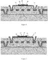
Figure 5 is a schematic diagram showing a process of forming a thermal sensitive layer according to the present disclosure. -
Figure 6 is a schematic diagram showing a process of forming a protection layer for the thermal sensitive layer and a contact hole according to the present disclosure. -
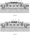
Figure 7 is a schematic diagram showing a process of forming a second metal electrode layer according to the present disclosure. -
Figure 8 is a schematic diagram showing a process of forming a second silicon nitride dielectric layer according to the present disclosure. -
Figure 9 is a schematic diagram showing a process of forming a thermal conversion structure of the second layer structure according to the present disclosure. -
Figure 10 is a schematic diagram showing a process of forming a third sacrificial layer, a third support layer, an absorption layer and a protection layer for the absorption layer according to the present disclosure. -
Figure 11 is a schematic diagram showing a process of forming a three-layer micro-bridge structure according to the present disclosure. -
Figure 12 is a graph comparing the absorbance of the pixel according to the present disclosure with that of a conventional pixel. - In the drawings, the correspondence between reference numerals and the elements is as follows.
- 1. semiconductor substrate, 2. metal reflection layer, 3. metal electrode block, 4. insulation dielectric layer, 51. first sacrificial layer, 52. second sacrificial layer, 53. third sacrificial layer, 6. first support layer, 7. protection layer for first support layer, 8. first through-hole, 9. first metal electrode layer, 91. metal wiring, 92. metal electrode, 10. first silicon nitride dielectric layer, 11. second support layer, 12. protection layer for second support layer, 13. second through-hole, 14. second metal electrode layer, 15. second silicon nitride dielectric layer, 16. contact hole, 17. thermal sensitive layer, 18. protection layer for thermal sensitive layer, 19. third support layer, 20. absorption layer, 21. protection layer for absorption layer.
- Hereinafter, the principles and features of the present disclosure will be described in conjunction with drawings. Embodiments are only for explaining the present disclosure and are not intended to limit the scope of the present disclosure.
- A method of preparing a pixel of an uncooled infrared focal plane detector includes the following steps 1 to 11.
- At step 1, as shown in
Figure 1 , a semiconductor substrate 1 including a readout integrated circuit (not shown) is provided; a metal layer is deposited on the semiconductor substrate 1. The metal layer is patterned to form ametal reflection layer 2 pattern and a metal electrode block 3, a thickness of themetal reflection layer 2 is from 0.05 to 0.40 µm. The metal electrode block 3 is electrically connected to the readout integrated circuit on the semiconductor substrate 1. Aninsulation dielectric layer 4 is deposited on the patterned metal layer, theinsulation dielectric layer 4 is a silicon nitride film or a SiO2 film having a stress from -50 to 100 MPa, and a thickness of theinsulation dielectric layer 4 is from 0.02 to 0.30 µm. A first sacrificial layer 51 is deposited on theinsulation dielectric layer 4, the first sacrificial layer 51 is one of an amorphous carbon, an amorphous silicon and a polyimide, and then a planarization processing is performed on the first sacrificial layer 51. A SiO2 film is deposited by a PECVD method on the first sacrificial layer 51 as afirst support layer 6 after the planarization processing is completed; and a silicon nitride film having a stress from -50 to 100 MPa is deposited on thefirst support layer 6 as a protection layer 7 for the first support layer; where a thickness of thefirst support layer 6 is from 0.05 to 0.30 µm. - At
step 2, as shown inFigure 2 , a first through-hole 8 is etched by a method of photolithography and reactive ion etching in a direction from the protection layer 7 for the first support layer to the semiconductor substrate 1, where the etching of the first through-hole 8 is ended at the metal electrode block 3 that is electrically connected to the readout integrated circuit. - At step 3, as shown in
Figure 3 , a first metal electrode layer 9 is deposited by a PVD method on the protection layer 7 for the first support layer and at the bottom of the first through-hole 8, where the first metal electrode layer 9 is one of a Ti film, a NiCr film and a TiN film, and a thickness of the first metal electrode layer 9 is from 50 to 1500 angstrom. The first metal electrode layer 9 is patterned to form ametal wiring 91 and ametal electrode 92. A first siliconnitride dielectric layer 10 is deposited by a PEVCD method on the patterned first metal electrode layer 9, where a thickness of the first siliconnitride dielectric layer 10 is from 200 to 2000 angstrom; and then vertically downward from the first siliconnitride dielectric layer 10, the first siliconnitride dielectric layer 10, the first metal electrode layer 9, the protection layer 7 for the first support layer and thefirst support layer 6 are sequentially etched, where the etching is ended at the first sacrificial layer 51. A bridge leg structure is formed; - At
step 4, as shown inFigure 4 , a secondsacrificial layer 52 is deposited on the bridge leg structure, where the secondsacrificial layer 52 is one of an amorphous carbon, an amorphous silicon, a silicon oxide and a polyimide, and a thickness of the secondsacrificial layer 52 is from 0.5 to 3 µm. Then, a planarization processing is performed on the secondsacrificial layer 52, a SiO2 film is deposited by a PECVD method as asecond support layer 11 on the secondsacrificial layer 52 after the planarization processing is completed, and a thickness of the second support layer is from 0.05 to 0.30µm. A silicon nitride film having a stress from -50 to 100 MPa is deposited by a PECVD method on thesecond support layer 11 as aprotection layer 12 for the second support layer, where a thickness of theprotection layer 12 for the second support layer is from 0.05 to 0.30µm. A second through-hole 13 is etched by a method of photolithography and reactive ion etching in a direction from theprotection layer 12 for the second support layer to the first metal electrode layer 9, where the etching of the second through-hole 13 is ended at the first metal electrode layer 9. - At step 5, as shown in
Figure 5 , a thermalsensitive layer 17 is deposited on theprotection layer 12 for the second support layer by a method of ion beam deposition or physical vapor deposition, where the thermalsensitive layer 17 is a VOx film or an amorphous silicon film, and a thickness of the thermalsensitive layer 17 is from 500 to 3000 angstrom. Before the deposition of the thermal sensitive layer, a layer of V/V2O5/V film is deposited as a buffer layer, where a thickness of the V/V2O5/V film is from 10 to 200 angstrom. The thermalsensitive layer 17 is patterned. - At
step 6, as shown inFigure 6 , a silicon nitride film having a stress from -50 to 100 MPa is deposited by a PECVD method as aprotection layer 18 for the thermal sensitive layer on the thermalsensitive layer 17 after the patterning process is completed, where a thickness of theprotection layer 18 for the thermal sensitive layer is from 200 to 2000 angstrom, and theprotection layer 18 for the thermal sensitive layer is patterned. Part of theprotection layer 18 for the thermal sensitive layer which is the thermalsensitive layer 17 is etched away by a method of photolithography and reactive ion etching performed on theprotection layer 18 for the thermal sensitive layer after the patterning process is completed, , , so as to form acontact hole 16 to expose the thermalsensitive layer 17, where thecontact hole 16 is etched using SF6, CHF3 and O2, or using CF4 and O2 as etching gas. Since the thickness of the mental electrode layer is extremely thin, an endpoint detecting device is used for monitoring an endpoint of the etching reaction during the etching process, thereby avoiding over etching the metal electrode layer. - At step 7, as shown in
Figure 7 , a secondmetal electrode layer 14 is deposited on theprotection layer 12 for the second support layer, theprotection layer 18 for the thermal sensitive layer, thecontact hole 16 and the bottom of the second through-hole 13 by a PVD method, where the secondmetal electrode layer 14 is one of a Ti film, a NiCr film and a TiN film, and a thickness of the secondmetal electrode layer 14 is from 50 to 1500 angstrom. The secondmetal electrode layer 14 is patterned. - At step 8, as shown in
Figure 8 , a second siliconnitride dielectric layer 15 is deposited by a PECVD method on the secondmetal electrode layer 14 after the patterning process is completed, where a thickness of the second siliconnitride dielectric layer 15 is from 200 to 2000 angstrom, and the second siliconnitride dielectric layer 15 is patterned. - At step 9, as shown in
Figure 9 , vertically downward from the second siliconnitride dielectric layer 15 after the patterning process is completed, the second siliconnitride dielectric layer 15, the secondmetal electrode layer 14, theprotection layer 18 for the thermal sensitive layer, the thermalsensitive layer 17, and theprotection layer 12 for the second support layer are sequentially etched, where the etching is ended at the secondsacrificial layer 52. A thermal conversion structure including micro bridge legs and a thermal sensitive structure is formed. - At
step 10, as shown inFigure 10 , a third sacrificial layer 53 is deposited on the thermal conversion structure including the micro bridge legs and the thermal sensitive structure, where the third sacrificial layer 53 is one of an amorphous carbon, an amorphous silicon, a silicon oxide and a polyimide and a thickness of the third sacrificial layer 53 is from 0.5 to 3µm. A planarization processing is performed on the third sacrificial layer 53, a SiO2 film is deposited by a PECVD method as athird support layer 19 on the third sacrificial layer 53 after the planarization processing is completed, where a thickness of thethird support layer 19 is from 0.05 to 0.30µm. An absorption layer film is deposited on thethird support layer 19 as anabsorption layer 20. A silicon nitride film having a stress from -50 to 100 MPa is deposited on theabsorption layer 20 as aprotection layer 21 for the absorption layer. The material of the absorption layer film is one of graphene, carbon nanotube, titanium dioxide nanotube, zinc oxide nanotube and alumina nanotube, and the thickness of theprotection layer 21 for the absorption layer is from 0.05 to 0.30 µm. A n absorption layer structure is formed. - A pixel of an uncooled infrared focal plane detector, as shown in
Figure 11 , includes a semiconductor substrate including a readout integrated circuit and a pixel of the detector having a three-layer structure, the pixel of the detector is electrically connected to the readout integrated circuit of the semiconductor substrate, - From the semiconductor substrate 1 upward, the pixel of the detector includes a structure sequentially having three layers, where the first layer is a bridge leg structure, the second layer is a thermal conversion structure, and the third layer is an absorption layer structure.
- The bridge leg structure at the first layer includes a
metal reflection layer 2, aninsulation dielectric layer 4, afirst support layer 6, a protection layer 7 for the first support layer, a first metal electrode layer 9 and a first siliconnitride dielectric layer 10. - The thermal conversion structure at the second layer includes a
second support layer 11, aprotection layer 12 for the second support layer, a thermalsensitive layer 17, aprotection layer 18 for the thermal sensitive layer, a secondmetal electrode layer 14, and a second siliconnitride dielectric layer 15. - The absorption layer structure of the third layer includes a
third support layer 19, anabsorption layer 20 and aprotection layer 21 for the absorption layer. - The
metal reflection layer 2 and theinsulation dielectric layer 4 are sequentially disposed on the readout integrated circuit of the semiconductor substrate 1. - The
first support layer 6 is disposed on theinsulation dielectric layer 4. - The protection layer 7 for the first support layer, the first metal electrode layer 9 and the first silicon
nitride dielectric layer 10 are sequentially disposed on thefirst support layer 6. - The
second support layer 11 is disposed on the first siliconnitride dielectric layer 10. - The
protection layer 12 for the second support layer, the thermalsensitive layer 17, theprotection layer 18 for the thermal sensitive layer, the secondmetal electrode layer 14 and the second silicon nitride dielectric layer 15) are sequentially disposed on thesecond support layer 11. - The
third support layer 19 is disposed on the second siliconnitride dielectric layer 15; - The
absorption layer 20 and theprotection layer 21 for the absorption layer are sequentially disposed on thethird support layer 19. - The
insulation dielectric layer 4 is a silicon nitride film; thefirst support layer 6 is a SiO2 film; the protection layer 7 for the first support layer is a silicon nitride film; thesecond support layer 11 is a SiO2 film; theprotection layer 12 for the second support layer is a silicon nitride film; the thermalsensitive layer 17 is a VOx film or an amorphous silicon film; theprotection layer 18 for the thermal sensitive layer is a silicon nitride film; and thethird support layer 19 is a SiO2 film. - As shown in
Figure 10 ,the absorption rate of a pixel according to the present disclosure is compared with that of a conventional pixel in the conventional technology. The pixel structure of the present disclosure has an absorption rate of more than 80% at a band from 3 to 14 µm, and has an absorption rate of more than 90% at a band from 8 to 14 µm. However, the structure in the conventional technology has a very low absorption rate at a band from 3 to 5 µm, which is only 15-40%, and has an absorption rate of only about 80% at the band from 8 to 14 µm. It can be seen that the uncooled infrared focal plane detector pixel according to the present disclosure can significantly improve the absorption rate of infrared radiation, broaden the infrared absorption spectrum range, and improve the response rate of the detector, thereby laying a foundation for manufacturing a detector with a larger array and a smaller pixel.
Claims (8)
- A method of preparing a pixel of an uncooled infrared focal plane detector, comprising:step 1, providing a semiconductor substrate (1) comprising a readout integrated circuit;depositing a metal layer on the semiconductor substrate (1);patterning the metal layer to form a metal reflection layer (2) pattern and a metal electrode block (3); wherein the metal electrode block (3) is electrically connected to the readout integrated circuit on the semiconductor substrate (1);depositing an insulation dielectric layer (4) on the patterned metal layer; depositing a first sacrificial layer (51) on the insulation dielectric layer (4), and performing a planarization processing on the first sacrificial layer (51);depositing a SiO2 film on the first sacrificial layer (51) as a first support layer (6) after the planarization processing is completed; anddepositing a silicon nitride film on the first support layer (6) as a protection layer (7) for the first support layer ;step 2, etching a first through-hole (8) by a method of photolithography and reactive ion etching in a direction from the protection layer (7) for the first support layer to the semiconductor substrate (1), wherein the etching of the first through-hole (8) is ended at the metal electrode block (3) that is electrically connected to the readout integrated circuit;step 3, depositing a first metal electrode layer (9) on the protection layer (7) for the first support layer and at the bottom of the first through-hole (8), and patterning the first metal electrode layer (9) to form a metal wiring (91) and a metal electrode (92);depositing a first silicon nitride dielectric layer (10) on the patterned first metal electrode layer (9); andsequentially etching, vertically downward from the first silicon nitride dielectric layer (10), the first silicon nitride dielectric layer (10), the first metal electrode layer (9), the protection layer (7) for the first support layer and the first support layer (6) to form a bridge leg structure, wherein the etching is ended at the first sacrificial layer (51);step 4, depositing a second sacrificial layer (52) on the bridge leg structure, and performing a planarization processing on the second sacrificial layer (52),depositing a SiO2 film as a second support layer (11) on the second sacrificial layer (52) after the planarization processing is completed;depositing a silicon nitride film on the second support layer (11) as a protection layer (12) for the second support layer;etching a second through-hole (13) by a method of photolithography and reactive ion etching in a direction from the protection layer (12) for the second support layer to the first metal electrode layer (9), wherein the etching of the second through-hole (13) is ended at the first metal electrode layer (9);step 5, depositing a thermal sensitive layer (17) on the protection layer (12) for the second support layer, and patterning the thermal sensitive layer;step 6, depositing a silicon nitride film as a protection layer (18) for the thermal sensitive layer on the thermal sensitive layer (17) after the patterning the thermal sensitive layer is completed,patterning the protection layer (18) for the thermal sensitive layer;etching, by a method of photolithography and reactive ion etching on the protection layer for the thermal sensitive layer (18) after the patterning the protection layer (18) for the thermal sensitive layer is completed, part of the protection layer (18) for the thermal sensitive layer which is on the thermal sensitive layer (17), such that and a contact hole (16) is formed to expose the thermal sensitive layer (17);step 7, depositing a second metal electrode layer (14) on the protection layer (12) for the second support layer, the protection layer (18) for the thermal sensitive layer, the contact hole (16) and the bottom of the second through-hole (13), and patterning the second metal electrode layer (14);step 8, depositing a second silicon nitride dielectric layer (15) on the second metal electrode layer (14) after the patterning the second metal electrode layer is completed, and patterning the second silicon nitride dielectric layer (15);step 9, sequentially etching, vertically downward from the second silicon nitride dielectric layer (15) after the patterning the second silicon nitride dielectric layer is completed, the second silicon nitride dielectric layer (15), the second metal electrode layer (14), the protection layer (18) for the thermal sensitive layer, the thermal sensitive layer (17), and the protection layer (12) for the second support layer, wherein the etching is ended at the second sacrificial layer (52), and a thermal conversion structure including micro bridge legs and a thermal sensitive structure is formed;step 10, depositing a third sacrificial layer (53) on the thermal conversion structure including the micro bridge legs and the thermal sensitive structure, and performing a planarization processing on the third sacrificial layer (53);depositing a SiO2 film as a third support layer (19) on the third sacrificial layer (53) after the planarization processing is completed;depositing an absorption layer film on the third support layer (19) as an absorption layer (20); anddepositing a silicon nitride film on the absorption layer (20) as a protection layer (21) of the absorption layer, and an absorption layer structure is formed;step 11, sequentially etching, vertically downward from the protection layer (21) of the absorption layer, the protection layer (21) of the absorption layer, the absorption layer (20) and the third support layer (19), wherein the etching is ended at the third sacrificial layer (53);removing the first sacrificial layer (51), the second sacrificial layer (52) and the third sacrificial layer (53), such that the pixel of the uncooled infrared focal plane detector is obtained.
- The method of preparing the pixel of the uncooled infrared focal plane detector according to claim 1, wherein at step 1, a thickness of the metal reflection layer (2) is from 0.05 to 0.40 µm; the insulation dielectric layer (4) is a silicon nitride film or a SiO2 film, a the thickness of the insulation dielectric layer (4) is from 0.02 to 0.30 µm; the first sacrificial layer (51) is one of amorphous carbon, amorphous silicon, and polyimide; the SiO2 film is deposited as the first support layer (6) by a PECVD method; and a thickness of the first support layer (6) is from 0.05 to 0.30 µm; the silicon nitride film is deposited as the protection layer (7) for the first support layer by a PECVD method; and a thickness of the protection layer (7) for the first support layer is from 0.05 to 0.30 µm.
- The method of preparing the pixel of the uncooled infrared focal plane detector according to claim 1, wherein at step 3, the first metal electrode layer (9) is deposited by a PVD method, and the first metal electrode layer (9) is one of a Ti film, a NiCr film and a TiN film; and a thickness of the first metal electrode layer (9) is from 50 to 1500 angstrom; the first silicon nitride dielectric layer (10) is deposited by a PEVCD method; and a thickness of the first silicon nitride dielectric layer (10) is from 200 to 2000 angstrom.
- The method of preparing the pixel of the uncooled infrared focal plane detector according to claim 1, wherein at step 4, the second sacrificial layer (52) is one of an amorphous carbon, an amorphous silicon, a silicon oxide and a polyimide; a thickness of the second sacrificial layer (52) is from 0.5 to 3 µm; the SiO2 film is deposited as the second support layer by a PECVD method; a thickness of the second support layer (11) is from 0.05 to 0.30 µm; the silicon nitride film is deposited as the protection layer (12) for the second support layer by a PECVD method, and a thickness of the protection layer (12) for the second support layer is from 0.05 to 0.30 µm.
- The method of preparing the pixel of the uncooled infrared focal plane detector according to claim 1, wherein at step 5, the thermal sensitive layer (17) is deposited by a method of ion beam deposition or physical vapor deposition; the thermal sensitive layer (17) is a VOx film or an amorphous silicon film; a thickness of the thermal sensitive layer (17) is from 500 to 3000 angstrom; a layer of V/V2O5/V film is deposited as a buffer layer before the depositing the thermal sensitive layer (17), a thickness of the V/V2O5/V film is from 10 to 200 angstrom;
wherein at step 6, the silicon nitride film is deposited as the protection layer (18) for the thermal sensitive layer by a PECVD method; a thickness of the protection layer (18) for the thermal sensitive layer is from 200 to 2000 angstrom; the contact hole is etched by using SF6, CHF3 and O2, or using CF4 and O2 as etching gas, and an endpoint detecting device is used for monitoring endpoints of the etching reactions. - The method of preparing the pixel of the uncooled infrared focal plane detector according to claim 1, wherein at step 7, the second metal electrode layer (14) is deposited by a PVD method, the second metal electrode layer (14) is one of a Ti film, a NiCr film and a TiN film, a thickness of the second metal electrode layer (14) is from 50 to 1500 angstrom; and
wherein at step 8, the second silicon nitride dielectric layer (15) is deposited by a PEVCD method, a thickness of the second silicon nitride dielectric layer (15) is from 200 to 2000 angstrom. - The method of preparing the pixel of the uncooled infrared focal plane detector according to claim 1, wherein at step 10, the third sacrificial layer (53) is one of an amorphous carbon, an amorphous silicon, a silicon oxide and a polyimide; a thickness of the third sacrificial layer (53) is from 0.5 to 3 µm; the SiO2 film is deposited as the third support layer (19) by a PECVD method; a thickness of the third support layer (19) is from 0.05 to 0.30 µm; materials of the film at the absorption layer is one of graphene, carbon nanotube, titanium dioxide nanotube, zinc oxide nanotube and an alumina nanotube; and a thickness of the protection layer (21) for the absorption layer is from 0.05 to 0.30 µm.
- The method of preparing the pixel of the uncooled infrared focal plane detector according to claim 1, wherein at step 11, the first sacrificial layer (51), the second sacrificial layer (52) and the third sacrificial layer (53) are removed by using a resist remover, an ion etching machine or a plasma ashing machine.
Applications Claiming Priority (1)
| Application Number | Priority Date | Filing Date | Title |
|---|---|---|---|
| PCT/CN2016/100865 WO2018058450A1 (en) | 2016-09-29 | 2016-09-29 | Pixel for uncooled infrared focal plane detector and preparation method therefor |
Publications (3)
| Publication Number | Publication Date |
|---|---|
| EP3522217A1 EP3522217A1 (en) | 2019-08-07 |
| EP3522217A4 EP3522217A4 (en) | 2020-05-13 |
| EP3522217B1 true EP3522217B1 (en) | 2021-07-14 |
Family
ID=61762360
Family Applications (1)
| Application Number | Title | Priority Date | Filing Date |
|---|---|---|---|
| EP16917204.6A Active EP3522217B1 (en) | 2016-09-29 | 2016-09-29 | Method to prepare pixel for uncooled infrared focal plane detector |
Country Status (3)
| Country | Link |
|---|---|
| US (1) | US10825857B2 (en) |
| EP (1) | EP3522217B1 (en) |
| WO (1) | WO2018058450A1 (en) |
Families Citing this family (11)
| Publication number | Priority date | Publication date | Assignee | Title |
|---|---|---|---|---|
| CN112071956B (en) * | 2020-09-08 | 2022-08-16 | 山西国惠光电科技有限公司 | Preparation process of novel InGaAs infrared focal plane detector |
| CN114112056A (en) * | 2021-03-26 | 2022-03-01 | 北京北方高业科技有限公司 | Infrared detector pixel and infrared detector based on CMOS (complementary metal oxide semiconductor) process |
| CN114112055B (en) * | 2021-03-26 | 2023-07-07 | 北京北方高业科技有限公司 | Infrared detector based on CMOS technology and preparation method thereof |
| SE544822C2 (en) * | 2021-04-13 | 2022-12-06 | Saab Ab | An antenna structure and method for manufacturing the same |
| CN113447142A (en) * | 2021-06-25 | 2021-09-28 | 北京北方高业科技有限公司 | Reinforced CMOS infrared detector |
| CN113948542B (en) * | 2021-10-19 | 2025-10-03 | 烟台睿创微纳技术股份有限公司 | A pixel-level packaging structure of an uncooled infrared detector and its manufacturing method |
| CN114001832B (en) * | 2021-10-29 | 2024-02-27 | 烟台睿创微纳技术股份有限公司 | An uncooled infrared polarization detection pixel structure, chip and detector |
| CN115425041B (en) * | 2022-09-26 | 2024-06-11 | 山西国惠光电科技有限公司 | A method for preparing an InGaAs infrared focal plane detector for suppressing electrical crosstalk |
| CN115900966B (en) * | 2022-10-25 | 2025-12-23 | 深圳先进技术研究院 | Thermosensitive film, infrared detector and preparation method of infrared detector |
| CN116558651B (en) * | 2023-05-25 | 2026-01-23 | 杭州大立微电子有限公司 | Uncooled focal plane infrared sensor and preparation method thereof |
| TWI887664B (en) * | 2023-05-31 | 2025-06-21 | 松翰科技股份有限公司 | Micro-bolometer and manufacturing method thereof |
Family Cites Families (30)
| Publication number | Priority date | Publication date | Assignee | Title |
|---|---|---|---|---|
| US891161A (en) | 1907-05-07 | 1908-06-16 | Percy H Goodwin | Automatic adjustable gem-holder. |
| US5821598A (en) * | 1995-02-01 | 1998-10-13 | Research Corporation Technologies, Inc. | Uncooled amorphous YBaCuO thin film infrared detector |
| US6690014B1 (en) | 2000-04-25 | 2004-02-10 | Raytheon Company | Microbolometer and method for forming |
| JP4612932B2 (en) * | 2000-06-01 | 2011-01-12 | ホーチキ株式会社 | Infrared detector and infrared two-dimensional image sensor |
| FR2822541B1 (en) * | 2001-03-21 | 2003-10-03 | Commissariat Energie Atomique | METHODS AND DEVICES FOR MANUFACTURING RADIATION DETECTORS |
| JP4135857B2 (en) | 2001-03-27 | 2008-08-20 | 独立行政法人産業技術総合研究所 | Infrared sensor manufacturing method |
| US6667479B2 (en) * | 2001-06-01 | 2003-12-23 | Raytheon Company | Advanced high speed, multi-level uncooled bolometer and method for fabricating same |
| JP2003106895A (en) * | 2001-10-01 | 2003-04-09 | Nec Corp | Thermal infrared detecting element and method of manufacturing the same |
| US7145143B2 (en) * | 2002-03-18 | 2006-12-05 | Honeywell International Inc. | Tunable sensor |
| US6891161B2 (en) | 2003-01-17 | 2005-05-10 | Drs Sensors & Targeting Systems, Inc. | Pixel structure and an associated method of fabricating the same |
| US7042622B2 (en) * | 2003-10-30 | 2006-05-09 | Reflectivity, Inc | Micromirror and post arrangements on substrates |
| US7019880B1 (en) * | 2004-08-25 | 2006-03-28 | Reflectivity, Inc | Micromirrors and hinge structures for micromirror arrays in projection displays |
| JP5597862B2 (en) | 2007-03-27 | 2014-10-01 | 日本電気株式会社 | Bolometer type THz wave detector |
| US8472100B2 (en) * | 2008-03-12 | 2013-06-25 | Texas Instruments Incorporated | Multilayered deformable element with reduced memory properties in a MEMS device |
| KR101183972B1 (en) * | 2008-12-16 | 2012-09-19 | 한국전자통신연구원 | bolometer structure with complemental absorption layer, pixel for IR detector using this and method for fabricating the same |
| JP5428783B2 (en) * | 2009-11-12 | 2014-02-26 | 日本電気株式会社 | Bolometer type THz wave detector |
| US8513605B2 (en) | 2010-04-28 | 2013-08-20 | L-3 Communications Corporation | Optically transitioning thermal detector structures |
| JP2012194080A (en) * | 2011-03-17 | 2012-10-11 | Nec Corp | Bolometer type thz wave detector |
| US9134527B2 (en) * | 2011-04-04 | 2015-09-15 | Qualcomm Mems Technologies, Inc. | Pixel via and methods of forming the same |
| US8963159B2 (en) * | 2011-04-04 | 2015-02-24 | Qualcomm Mems Technologies, Inc. | Pixel via and methods of forming the same |
| CN102951597B (en) * | 2011-08-19 | 2016-03-30 | 烟台睿创微纳技术有限公司 | A kind of preparation method of infrared detector with micro-bridge structure and micro-bridge structure |
| US9261411B2 (en) * | 2012-12-19 | 2016-02-16 | Institut National D'optique | Uncooled microbolometer detector and array for terahertz detection |
| CN103112817B (en) * | 2013-02-04 | 2016-01-13 | 烟台睿创微纳技术有限公司 | A kind of non-refrigerated infrared detector tower pier and preparation method thereof |
| US9646874B1 (en) * | 2013-08-05 | 2017-05-09 | Sandia Corporation | Thermally-isolated silicon-based integrated circuits and related methods |
| CN103715307B (en) | 2013-12-31 | 2016-01-13 | 烟台睿创微纳技术有限公司 | A kind of non-refrigerated infrared detector and preparation method thereof |
| CN103759838B (en) * | 2014-01-13 | 2016-06-01 | 浙江大立科技股份有限公司 | Infrared detector with micro-bridge structure and manufacture method thereof |
| CN103776546A (en) * | 2014-01-21 | 2014-05-07 | 武汉高芯科技有限公司 | Non-refrigeration infrared focal plane array detector of double-layer structure |
| CN105486412A (en) | 2015-12-31 | 2016-04-13 | 武汉高芯科技有限公司 | Uncooled infrared focal plane array detector with overlap vertical bridge legs |
| FR3050526B1 (en) * | 2016-04-25 | 2018-05-25 | Commissariat A L'energie Atomique Et Aux Energies Alternatives | ELECTROMAGNETIC RADIATION DETECTION DEVICE WITH ENCAPSULATION STRUCTURE HAVING AT LEAST ONE INTERFERENTIAL FILTER |
| CN106298827B (en) * | 2016-09-29 | 2018-07-31 | 烟台睿创微纳技术股份有限公司 | A kind of non-refrigerated infrared focal plane probe pixel and preparation method thereof |
-
2016
- 2016-09-29 EP EP16917204.6A patent/EP3522217B1/en active Active
- 2016-09-29 US US16/337,868 patent/US10825857B2/en active Active
- 2016-09-29 WO PCT/CN2016/100865 patent/WO2018058450A1/en not_active Ceased
Also Published As
| Publication number | Publication date |
|---|---|
| EP3522217A4 (en) | 2020-05-13 |
| EP3522217A1 (en) | 2019-08-07 |
| US20200027916A1 (en) | 2020-01-23 |
| US10825857B2 (en) | 2020-11-03 |
| WO2018058450A1 (en) | 2018-04-05 |
Similar Documents
| Publication | Publication Date | Title |
|---|---|---|
| US10825857B2 (en) | Pixel for uncooled infrared focal plane detector and preparation method therefor | |
| CN106298827B (en) | A kind of non-refrigerated infrared focal plane probe pixel and preparation method thereof | |
| CN106352989B (en) | Fabrication method and structure of an uncooled infrared focal plane detector microbridge | |
| CN103715307B (en) | A kind of non-refrigerated infrared detector and preparation method thereof | |
| JP5597862B2 (en) | Bolometer type THz wave detector | |
| CN106340561A (en) | Novel uncooled infrared focal plane detector pixel and fabrication method thereof | |
| KR100925214B1 (en) | Volometer and its manufacturing method | |
| CN106784165B (en) | A kind of novel double-layer non-refrigerated infrared focal plane probe dot structure and preparation method thereof | |
| WO2012071820A1 (en) | Infrared detector and method of manufacture thereof and multi-band uncooled infrared focal plane | |
| US8895924B2 (en) | Infrared detector based on suspended bolometric micro-plates | |
| US7268349B2 (en) | Infrared absorption layer structure and its formation method, and an uncooled infrared detector using this structure | |
| CN202329818U (en) | Uncooled infrared detection device | |
| CN102951597A (en) | Preparation method of micro-bridge structured infrared detector, and micro-bridge structure | |
| CN106082106B (en) | A kind of broadband non-refrigerated infrared detector and preparation method thereof | |
| JP2012194080A (en) | Bolometer type thz wave detector | |
| CN106124066A (en) | The microbolometer of a kind of high fill factor and preparation method | |
| CN110118604A (en) | Wide spectrum micro-metering bolometer and preparation method thereof based on hybrid resonant mode | |
| JP2016070935A (en) | Bolometric detector having mim structure of different dimensions | |
| CN107055464A (en) | A kind of method for using amorphous carbon to make micro-metering bolometer micro-bridge structure as sacrifice layer | |
| CN107253696B (en) | Pixel structure of a microbolometer and preparation method thereof | |
| CN202066596U (en) | Infrared detector and multiband uncooled infrared focal plane | |
| CN105811061A (en) | Bridge leg separated antenna coupling micro-bridge structure and fabrication method thereof | |
| CN106800271B (en) | A kind of non-refrigerated infrared focal plane probe dot structure and preparation method thereof | |
| KR100539395B1 (en) | Uncooled infrared sensor with two-layer structure | |
| CN106847950A (en) | Ion implanting prepares Infrared Detectors of Titanium oxide electrode and preparation method thereof |
Legal Events
| Date | Code | Title | Description |
|---|---|---|---|
| STAA | Information on the status of an ep patent application or granted ep patent |
Free format text: STATUS: THE INTERNATIONAL PUBLICATION HAS BEEN MADE |
|
| PUAI | Public reference made under article 153(3) epc to a published international application that has entered the european phase |
Free format text: ORIGINAL CODE: 0009012 |
|
| STAA | Information on the status of an ep patent application or granted ep patent |
Free format text: STATUS: REQUEST FOR EXAMINATION WAS MADE |
|
| 17P | Request for examination filed |
Effective date: 20190411 |
|
| AK | Designated contracting states |
Kind code of ref document: A1 Designated state(s): AL AT BE BG CH CY CZ DE DK EE ES FI FR GB GR HR HU IE IS IT LI LT LU LV MC MK MT NL NO PL PT RO RS SE SI SK SM TR |
|
| AX | Request for extension of the european patent |
Extension state: BA ME |
|
| DAV | Request for validation of the european patent (deleted) | ||
| DAX | Request for extension of the european patent (deleted) | ||
| A4 | Supplementary search report drawn up and despatched |
Effective date: 20200409 |
|
| RIC1 | Information provided on ipc code assigned before grant |
Ipc: H01L 27/146 20060101AFI20200403BHEP |
|
| GRAP | Despatch of communication of intention to grant a patent |
Free format text: ORIGINAL CODE: EPIDOSNIGR1 |
|
| STAA | Information on the status of an ep patent application or granted ep patent |
Free format text: STATUS: GRANT OF PATENT IS INTENDED |
|
| INTG | Intention to grant announced |
Effective date: 20210202 |
|
| GRAS | Grant fee paid |
Free format text: ORIGINAL CODE: EPIDOSNIGR3 |
|
| GRAA | (expected) grant |
Free format text: ORIGINAL CODE: 0009210 |
|
| STAA | Information on the status of an ep patent application or granted ep patent |
Free format text: STATUS: THE PATENT HAS BEEN GRANTED |
|
| AK | Designated contracting states |
Kind code of ref document: B1 Designated state(s): AL AT BE BG CH CY CZ DE DK EE ES FI FR GB GR HR HU IE IS IT LI LT LU LV MC MK MT NL NO PL PT RO RS SE SI SK SM TR |
|
| REG | Reference to a national code |
Ref country code: GB Ref legal event code: FG4D |
|
| RAP4 | Party data changed (patent owner data changed or rights of a patent transferred) |
Owner name: YANTAI RAYTRON TECHNOLOGY CO., LTD |
|
| REG | Reference to a national code |
Ref country code: DE Ref legal event code: R096 Ref document number: 602016060788 Country of ref document: DE |
|
| REG | Reference to a national code |
Ref country code: IE Ref legal event code: FG4D |
|
| REG | Reference to a national code |
Ref country code: DE Ref legal event code: R081 Ref document number: 602016060788 Country of ref document: DE Owner name: YANTAI RAYTRON TECHNOLOGY CO., LTD, CN Free format text: FORMER OWNER: YANTAI RAYTRON TECHNOLOGY CO., LTD., YANTAI, SHANDONG, CN |
|
| REG | Reference to a national code |
Ref country code: AT Ref legal event code: REF Ref document number: 1411321 Country of ref document: AT Kind code of ref document: T Effective date: 20210815 |
|
| REG | Reference to a national code |
Ref country code: LT Ref legal event code: MG9D |
|
| REG | Reference to a national code |
Ref country code: NL Ref legal event code: MP Effective date: 20210714 |
|
| REG | Reference to a national code |
Ref country code: AT Ref legal event code: MK05 Ref document number: 1411321 Country of ref document: AT Kind code of ref document: T Effective date: 20210714 |
|
| PG25 | Lapsed in a contracting state [announced via postgrant information from national office to epo] |
Ref country code: BG Free format text: LAPSE BECAUSE OF FAILURE TO SUBMIT A TRANSLATION OF THE DESCRIPTION OR TO PAY THE FEE WITHIN THE PRESCRIBED TIME-LIMIT Effective date: 20211014 Ref country code: AT Free format text: LAPSE BECAUSE OF FAILURE TO SUBMIT A TRANSLATION OF THE DESCRIPTION OR TO PAY THE FEE WITHIN THE PRESCRIBED TIME-LIMIT Effective date: 20210714 Ref country code: LT Free format text: LAPSE BECAUSE OF FAILURE TO SUBMIT A TRANSLATION OF THE DESCRIPTION OR TO PAY THE FEE WITHIN THE PRESCRIBED TIME-LIMIT Effective date: 20210714 Ref country code: ES Free format text: LAPSE BECAUSE OF FAILURE TO SUBMIT A TRANSLATION OF THE DESCRIPTION OR TO PAY THE FEE WITHIN THE PRESCRIBED TIME-LIMIT Effective date: 20210714 Ref country code: FI Free format text: LAPSE BECAUSE OF FAILURE TO SUBMIT A TRANSLATION OF THE DESCRIPTION OR TO PAY THE FEE WITHIN THE PRESCRIBED TIME-LIMIT Effective date: 20210714 Ref country code: HR Free format text: LAPSE BECAUSE OF FAILURE TO SUBMIT A TRANSLATION OF THE DESCRIPTION OR TO PAY THE FEE WITHIN THE PRESCRIBED TIME-LIMIT Effective date: 20210714 Ref country code: NO Free format text: LAPSE BECAUSE OF FAILURE TO SUBMIT A TRANSLATION OF THE DESCRIPTION OR TO PAY THE FEE WITHIN THE PRESCRIBED TIME-LIMIT Effective date: 20211014 Ref country code: NL Free format text: LAPSE BECAUSE OF FAILURE TO SUBMIT A TRANSLATION OF THE DESCRIPTION OR TO PAY THE FEE WITHIN THE PRESCRIBED TIME-LIMIT Effective date: 20210714 Ref country code: PT Free format text: LAPSE BECAUSE OF FAILURE TO SUBMIT A TRANSLATION OF THE DESCRIPTION OR TO PAY THE FEE WITHIN THE PRESCRIBED TIME-LIMIT Effective date: 20211115 Ref country code: SE Free format text: LAPSE BECAUSE OF FAILURE TO SUBMIT A TRANSLATION OF THE DESCRIPTION OR TO PAY THE FEE WITHIN THE PRESCRIBED TIME-LIMIT Effective date: 20210714 Ref country code: RS Free format text: LAPSE BECAUSE OF FAILURE TO SUBMIT A TRANSLATION OF THE DESCRIPTION OR TO PAY THE FEE WITHIN THE PRESCRIBED TIME-LIMIT Effective date: 20210714 |
|
| PG25 | Lapsed in a contracting state [announced via postgrant information from national office to epo] |
Ref country code: PL Free format text: LAPSE BECAUSE OF FAILURE TO SUBMIT A TRANSLATION OF THE DESCRIPTION OR TO PAY THE FEE WITHIN THE PRESCRIBED TIME-LIMIT Effective date: 20210714 Ref country code: LV Free format text: LAPSE BECAUSE OF FAILURE TO SUBMIT A TRANSLATION OF THE DESCRIPTION OR TO PAY THE FEE WITHIN THE PRESCRIBED TIME-LIMIT Effective date: 20210714 Ref country code: GR Free format text: LAPSE BECAUSE OF FAILURE TO SUBMIT A TRANSLATION OF THE DESCRIPTION OR TO PAY THE FEE WITHIN THE PRESCRIBED TIME-LIMIT Effective date: 20211015 |
|
| REG | Reference to a national code |
Ref country code: DE Ref legal event code: R097 Ref document number: 602016060788 Country of ref document: DE |
|
| PG25 | Lapsed in a contracting state [announced via postgrant information from national office to epo] |
Ref country code: DK Free format text: LAPSE BECAUSE OF FAILURE TO SUBMIT A TRANSLATION OF THE DESCRIPTION OR TO PAY THE FEE WITHIN THE PRESCRIBED TIME-LIMIT Effective date: 20210714 |
|
| REG | Reference to a national code |
Ref country code: CH Ref legal event code: PL |
|
| PLBE | No opposition filed within time limit |
Free format text: ORIGINAL CODE: 0009261 |
|
| REG | Reference to a national code |
Ref country code: BE Ref legal event code: MM Effective date: 20210930 |
|
| STAA | Information on the status of an ep patent application or granted ep patent |
Free format text: STATUS: NO OPPOSITION FILED WITHIN TIME LIMIT |
|
| PG25 | Lapsed in a contracting state [announced via postgrant information from national office to epo] |
Ref country code: SM Free format text: LAPSE BECAUSE OF FAILURE TO SUBMIT A TRANSLATION OF THE DESCRIPTION OR TO PAY THE FEE WITHIN THE PRESCRIBED TIME-LIMIT Effective date: 20210714 Ref country code: SK Free format text: LAPSE BECAUSE OF FAILURE TO SUBMIT A TRANSLATION OF THE DESCRIPTION OR TO PAY THE FEE WITHIN THE PRESCRIBED TIME-LIMIT Effective date: 20210714 Ref country code: RO Free format text: LAPSE BECAUSE OF FAILURE TO SUBMIT A TRANSLATION OF THE DESCRIPTION OR TO PAY THE FEE WITHIN THE PRESCRIBED TIME-LIMIT Effective date: 20210714 Ref country code: MC Free format text: LAPSE BECAUSE OF FAILURE TO SUBMIT A TRANSLATION OF THE DESCRIPTION OR TO PAY THE FEE WITHIN THE PRESCRIBED TIME-LIMIT Effective date: 20210714 Ref country code: EE Free format text: LAPSE BECAUSE OF FAILURE TO SUBMIT A TRANSLATION OF THE DESCRIPTION OR TO PAY THE FEE WITHIN THE PRESCRIBED TIME-LIMIT Effective date: 20210714 Ref country code: CZ Free format text: LAPSE BECAUSE OF FAILURE TO SUBMIT A TRANSLATION OF THE DESCRIPTION OR TO PAY THE FEE WITHIN THE PRESCRIBED TIME-LIMIT Effective date: 20210714 Ref country code: AL Free format text: LAPSE BECAUSE OF FAILURE TO SUBMIT A TRANSLATION OF THE DESCRIPTION OR TO PAY THE FEE WITHIN THE PRESCRIBED TIME-LIMIT Effective date: 20210714 |
|
| 26N | No opposition filed |
Effective date: 20220419 |
|
| GBPC | Gb: european patent ceased through non-payment of renewal fee |
Effective date: 20211014 |
|
| PG25 | Lapsed in a contracting state [announced via postgrant information from national office to epo] |
Ref country code: LU Free format text: LAPSE BECAUSE OF NON-PAYMENT OF DUE FEES Effective date: 20210929 Ref country code: IT Free format text: LAPSE BECAUSE OF FAILURE TO SUBMIT A TRANSLATION OF THE DESCRIPTION OR TO PAY THE FEE WITHIN THE PRESCRIBED TIME-LIMIT Effective date: 20210714 Ref country code: IE Free format text: LAPSE BECAUSE OF NON-PAYMENT OF DUE FEES Effective date: 20210929 Ref country code: GB Free format text: LAPSE BECAUSE OF NON-PAYMENT OF DUE FEES Effective date: 20211014 Ref country code: BE Free format text: LAPSE BECAUSE OF NON-PAYMENT OF DUE FEES Effective date: 20210930 |
|
| PG25 | Lapsed in a contracting state [announced via postgrant information from national office to epo] |
Ref country code: LI Free format text: LAPSE BECAUSE OF NON-PAYMENT OF DUE FEES Effective date: 20210930 Ref country code: CH Free format text: LAPSE BECAUSE OF NON-PAYMENT OF DUE FEES Effective date: 20210930 |
|
| PG25 | Lapsed in a contracting state [announced via postgrant information from national office to epo] |
Ref country code: CY Free format text: LAPSE BECAUSE OF FAILURE TO SUBMIT A TRANSLATION OF THE DESCRIPTION OR TO PAY THE FEE WITHIN THE PRESCRIBED TIME-LIMIT Effective date: 20210714 |
|
| PG25 | Lapsed in a contracting state [announced via postgrant information from national office to epo] |
Ref country code: HU Free format text: LAPSE BECAUSE OF FAILURE TO SUBMIT A TRANSLATION OF THE DESCRIPTION OR TO PAY THE FEE WITHIN THE PRESCRIBED TIME-LIMIT; INVALID AB INITIO Effective date: 20160929 |
|
| PG25 | Lapsed in a contracting state [announced via postgrant information from national office to epo] |
Ref country code: MK Free format text: LAPSE BECAUSE OF FAILURE TO SUBMIT A TRANSLATION OF THE DESCRIPTION OR TO PAY THE FEE WITHIN THE PRESCRIBED TIME-LIMIT Effective date: 20210714 |
|
| PG25 | Lapsed in a contracting state [announced via postgrant information from national office to epo] |
Ref country code: TR Free format text: LAPSE BECAUSE OF FAILURE TO SUBMIT A TRANSLATION OF THE DESCRIPTION OR TO PAY THE FEE WITHIN THE PRESCRIBED TIME-LIMIT Effective date: 20210714 |
|
| PG25 | Lapsed in a contracting state [announced via postgrant information from national office to epo] |
Ref country code: MT Free format text: LAPSE BECAUSE OF FAILURE TO SUBMIT A TRANSLATION OF THE DESCRIPTION OR TO PAY THE FEE WITHIN THE PRESCRIBED TIME-LIMIT Effective date: 20210714 |
|
| REG | Reference to a national code |
Ref country code: DE Ref legal event code: R079 Ref document number: 602016060788 Country of ref document: DE Free format text: PREVIOUS MAIN CLASS: H01L0027146000 Ipc: H10F0039180000 |
|
| PGFP | Annual fee paid to national office [announced via postgrant information from national office to epo] |
Ref country code: DE Payment date: 20250926 Year of fee payment: 10 |
|
| PGFP | Annual fee paid to national office [announced via postgrant information from national office to epo] |
Ref country code: FR Payment date: 20250929 Year of fee payment: 10 |