EP3521783A1 - Terahertz detector - Google Patents
Terahertz detector Download PDFInfo
- Publication number
- EP3521783A1 EP3521783A1 EP18248030.1A EP18248030A EP3521783A1 EP 3521783 A1 EP3521783 A1 EP 3521783A1 EP 18248030 A EP18248030 A EP 18248030A EP 3521783 A1 EP3521783 A1 EP 3521783A1
- Authority
- EP
- European Patent Office
- Prior art keywords
- terahertz
- signal
- detector
- avalanche photodiode
- sensitive unit
- Prior art date
- Legal status (The legal status is an assumption and is not a legal conclusion. Google has not performed a legal analysis and makes no representation as to the accuracy of the status listed.)
- Granted
Links
Images


Classifications
-
- G—PHYSICS
- G01—MEASURING; TESTING
- G01J—MEASUREMENT OF INTENSITY, VELOCITY, SPECTRAL CONTENT, POLARISATION, PHASE OR PULSE CHARACTERISTICS OF INFRARED, VISIBLE OR ULTRAVIOLET LIGHT; COLORIMETRY; RADIATION PYROMETRY
- G01J1/00—Photometry, e.g. photographic exposure meter
- G01J1/02—Details
- G01J1/04—Optical or mechanical part supplementary adjustable parts
- G01J1/0407—Optical elements not provided otherwise, e.g. manifolds, windows, holograms, gratings
- G01J1/0411—Optical elements not provided otherwise, e.g. manifolds, windows, holograms, gratings using focussing or collimating elements, i.e. lenses or mirrors; Aberration correction
-
- G—PHYSICS
- G01—MEASURING; TESTING
- G01N—INVESTIGATING OR ANALYSING MATERIALS BY DETERMINING THEIR CHEMICAL OR PHYSICAL PROPERTIES
- G01N21/00—Investigating or analysing materials by the use of optical means, i.e. using sub-millimetre waves, infrared, visible or ultraviolet light
- G01N21/17—Systems in which incident light is modified in accordance with the properties of the material investigated
- G01N21/25—Colour; Spectral properties, i.e. comparison of effect of material on the light at two or more different wavelengths or wavelength bands
- G01N21/31—Investigating relative effect of material at wavelengths characteristic of specific elements or molecules, e.g. atomic absorption spectrometry
- G01N21/35—Investigating relative effect of material at wavelengths characteristic of specific elements or molecules, e.g. atomic absorption spectrometry using infrared light
- G01N21/3581—Investigating relative effect of material at wavelengths characteristic of specific elements or molecules, e.g. atomic absorption spectrometry using infrared light using far infrared light; using Terahertz radiation
-
- G—PHYSICS
- G01—MEASURING; TESTING
- G01J—MEASUREMENT OF INTENSITY, VELOCITY, SPECTRAL CONTENT, POLARISATION, PHASE OR PULSE CHARACTERISTICS OF INFRARED, VISIBLE OR ULTRAVIOLET LIGHT; COLORIMETRY; RADIATION PYROMETRY
- G01J1/00—Photometry, e.g. photographic exposure meter
- G01J1/42—Photometry, e.g. photographic exposure meter using electric radiation detectors
-
- G—PHYSICS
- G01—MEASURING; TESTING
- G01J—MEASUREMENT OF INTENSITY, VELOCITY, SPECTRAL CONTENT, POLARISATION, PHASE OR PULSE CHARACTERISTICS OF INFRARED, VISIBLE OR ULTRAVIOLET LIGHT; COLORIMETRY; RADIATION PYROMETRY
- G01J1/00—Photometry, e.g. photographic exposure meter
- G01J1/42—Photometry, e.g. photographic exposure meter using electric radiation detectors
- G01J1/44—Electric circuits
-
- H—ELECTRICITY
- H10—SEMICONDUCTOR DEVICES; ELECTRIC SOLID-STATE DEVICES NOT OTHERWISE PROVIDED FOR
- H10F—INORGANIC SEMICONDUCTOR DEVICES SENSITIVE TO INFRARED RADIATION, LIGHT, ELECTROMAGNETIC RADIATION OF SHORTER WAVELENGTH OR CORPUSCULAR RADIATION
- H10F30/00—Individual radiation-sensitive semiconductor devices in which radiation controls the flow of current through the devices, e.g. photodetectors
- H10F30/20—Individual radiation-sensitive semiconductor devices in which radiation controls the flow of current through the devices, e.g. photodetectors the devices having potential barriers, e.g. phototransistors
- H10F30/29—Individual radiation-sensitive semiconductor devices in which radiation controls the flow of current through the devices, e.g. photodetectors the devices having potential barriers, e.g. phototransistors the devices being sensitive to radiation having very short wavelengths, e.g. X-rays, gamma-rays or corpuscular radiation
-
- H—ELECTRICITY
- H10—SEMICONDUCTOR DEVICES; ELECTRIC SOLID-STATE DEVICES NOT OTHERWISE PROVIDED FOR
- H10F—INORGANIC SEMICONDUCTOR DEVICES SENSITIVE TO INFRARED RADIATION, LIGHT, ELECTROMAGNETIC RADIATION OF SHORTER WAVELENGTH OR CORPUSCULAR RADIATION
- H10F77/00—Constructional details of devices covered by this subclass
- H10F77/95—Circuit arrangements
- H10F77/953—Circuit arrangements for devices having potential barriers
- H10F77/959—Circuit arrangements for devices having potential barriers for devices working in avalanche mode
-
- G—PHYSICS
- G01—MEASURING; TESTING
- G01J—MEASUREMENT OF INTENSITY, VELOCITY, SPECTRAL CONTENT, POLARISATION, PHASE OR PULSE CHARACTERISTICS OF INFRARED, VISIBLE OR ULTRAVIOLET LIGHT; COLORIMETRY; RADIATION PYROMETRY
- G01J1/00—Photometry, e.g. photographic exposure meter
- G01J1/42—Photometry, e.g. photographic exposure meter using electric radiation detectors
- G01J1/44—Electric circuits
- G01J2001/4446—Type of detector
- G01J2001/446—Photodiode
- G01J2001/4466—Avalanche
-
- G—PHYSICS
- G01—MEASURING; TESTING
- G01J—MEASUREMENT OF INTENSITY, VELOCITY, SPECTRAL CONTENT, POLARISATION, PHASE OR PULSE CHARACTERISTICS OF INFRARED, VISIBLE OR ULTRAVIOLET LIGHT; COLORIMETRY; RADIATION PYROMETRY
- G01J1/00—Photometry, e.g. photographic exposure meter
- G01J1/42—Photometry, e.g. photographic exposure meter using electric radiation detectors
- G01J1/44—Electric circuits
- G01J2001/4446—Type of detector
- G01J2001/448—Array [CCD]
Definitions
- Embodiments of the present disclosure relate to detection technical field, and particularly to a terahertz detector.
- Terahertz wave is between a millimeter wave and an infrared wave and thus not only has certain penetration ability like the millimeter wave but also involves a relative high resolving ability like the infrared wave.
- the terahertz wave becomes used in security inspection of baggage, package or other items and human body security inspection.
- Applications of the terahertz wave are developed gradually. However, it is lacked currently to obtain a method of efficiently generating a terahertz wave and an accurate detecting method by using a terahertz wave.
- a terahertz detector is needed to be studied continuously.
- Detection using a terahertz wave may be classified in technology into two type, i.e., one is coherent detection and the other is non-coherent detection. Due to low outputting power of a terahertz radiation, loss of transfer, heat radiation and noise, et al., a terahertz signal that is detectable is rather weak. Thus, it is in dire need of a terahertz detector with high sensitivity during development of terahertz technology. In the context, many types of terahertz wave detectors are developing. A heat radiation meter is a non-coherent detection that can detect power of a radiation and is not able to report phase information. Further, this type detector commonly works at low temperature in order to reduce detection noise.
- a pyroelectric transducer has a relative simple structure and operation, and may work in normal temperature. However, a response time of a pyroelectric transducer depends on process of establishing a new balance temperature, that is, a pyroelectric transducer cannot detect a terahertz signal during changing of temperature.
- a Golay detector has a wide response frequency band, a low equivalent power of noise, a high response sensitivity and may operate at normal temperature. However, the Golay detector is sensitive to vibration and has a bad stability as a whole.
- counting type terahertz detector such as a single electron transistor detector and a quantum cascade laser, which is mainly used to detect photon at a frequency more than 1THz while having not effect for a low energy photon at a frequency less than ITHz.
- a whole apparatus of counting type terahertz detector is very expensive and is needed to work at super low temperature, and thus is limited to be used widely.
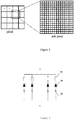
- FIG. 1 schematic plan views of a planar array structure constituted by a plurality of pixel units and of each of the pixel units according to an embodiment of the present disclosure are illustrated.
- Figure 1 schematically illustrates a relationship between the pixel units and a sub pixel of a counting-liked type terahertz detector according to an embodiment of the present disclosure.
- each of the pixel units may individually provide a signal, like a common image sensor (CMOS) pixel unit or CCD pixel unit.
- CMOS common image sensor
- Each of the pixel units of the counting-liked type terahertz detector according to the present embodiment is constituted by a plurality of sub pixels and each of the sub pixels may include no more than one signal trigger configured to transform a terahertz signal to an electrical current pulsing signal and may be a smaller pixel unit, as shown in Figure 1 .
- the pixel units form a planar array structure and each of the pixel units includes a plurality of sub pixels that may form a planar array structure.
- the plurality of sub pixels of each of the pixel units are connected in parallel, that is, an output signal of each of the sub pixels may be superimposed or added together and a result output signal having a superimposed amplitude is represented as a signal of a single pixel unit.
- each of the pixel units outputs a signal individually.
- FIG. 2 illustrates an equivalent circuit diagram of a single pixel unit of the terahertz detector according to an embodiment of the present disclosure.
- each of the pixel units is formed by a plurality of sub pixels that are connected in parallel.
- Each of the sub pixels may respectively include a terahertz wave sensitive unit 10, a Geiger avalanche photodiode 20 and quenching resistor 30.
- each sub pixel may include other elements.
- each sub pixel may include no quenching resistor 30.
- the sub pixels connected in parallel output a superimposed signal, which obviously is stronger than a signal outputted by any one of the sub pixels. Thus, an enhanced output signal may be obtained.
- the terahertz wave sensitive unit 10 may be a Schottky diode (SBD) detector 103, a high-speed electron mobility transistor 104 (HEMT), a complementary metal oxide semiconductor (CMOS) field effect transistor 104, or may be made of a pyroelectricity material, a graphene material, or may have a structure such as nano-line material, that may transform a terahertz signal to an electric signal.
- the Geiger avalanche photodiode (APD) 20 may be an avalanche photodiode that is under a breakdown state. In general, an equivalent resistance portion that is made of polysilicon or other highly-resistant material is integrated in an electrode of the Geiger avalanche photodiode 20.
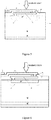
- Figure 3 shows a work principle view of a single sub pixel of a terahertz detector according to an embodiment of the present disclosure.
- the sensitive unit 10 When a sub pixel receives no terahertz signal, the sensitive unit 10 outputs a small and weak signal and thus the Geiger avalanche photodiode 20 (APD) is still in an initial breakdown state under action of a bias voltage.
- APD Geiger avalanche photodiode 20
- the front-end sensitive unit 10 transforms the terahertz signal to an electric signal and the electric signal may be transformed into a voltage signal and applied to the Geiger avalanche photodiode 20 (APD), such that the Geiger avalanche photodiode 20 that is in the initial breakdown state is excited to avalanche, thereby outputting a transient electrical current pulsing signal.
- APD Geiger avalanche photodiode 20
- the electrical current pulsing signal outputted by each of the sub pixels due to excitation of the terahertz signal may be considered as a branch signal of a pixel unit.
- the sensitive unit 10 located at a front position transforms a weak terahertz signal to an electrical current pulsing signal and the electrical current pulsing signal, after passing through a low noise amplifier, is passed to a subsequent read circuit such that the whole image system is simplified and may directly detect a weak terahertz signal.
- integration of the sensitive unit 10 located at a front position, the Geiger avalanche photodiode 20 and the quenching resistor 30 in one sub pixel may further optimize matched impedance of the components, increase a transformation efficiency of signal and increase the whole reliability of the device.
- FIG. 4 a work process of a single pixel unit of the counting-liked type detector according to an embodiment of the present disclosure is shown.
- a work process of a single sub pixel is described and a single pixel unit is formed by a plurality of sub pixels that are connected in parallel.
- a value of an output signal of the pixel unit is resulted from superimposing the electrical current pulsing signals outputted by the sub pixels that are excited by the terahertz signal.
- the amplitude of the superimposed electrical current pulsing signals is an integral times of an amplitude of the electrical current pulsing signal outputted by the single sub pixel under excitation of the terahertz signal.
- the pixel unit will output an electrical current pulsing signal having a amplitude of NA (assuming electrical current pulsing signals of the sub pixels to be equal to each other).
- the resulting electrical current pulsing signal having passed the low noise amplifier, is passed to the subsequent read circuit for signal processing.
- the sub pixels may respectively output electrical current pulsing signals that are different from one another.
- the sensitive units may be in various types.
- the amplitude of the electrical current pulsing signal outputted by the pixel unit may be NA. If the sensitive units have different specifications, the amplitude of the electrical current pulsing signal outputted by the pixel unit may be a superimposed value of the amplitudes of the electrical current pulsing signals outputted by the sensitive unites.
- Embodiments of the present disclosure include a plurality of sub pixels that may be formed by various types of sensitive units and form a pixel unit.
- the sensitive unit 10 located in the front position in the embodiment may be provided with an antenna structure to enhance collection of the terahertz signal.
- a size of the sensitive unit 10 may be determined according to a structure and size of the sub pixel.
- the antenna structure may be replaced by a super material to enhance collection of the terahertz signal.
- the sensitive unit 10 includes an antenna with a microstructure configured to enhance a terahertz signal towards at least one point of the sensitive unit 10.
- the microstructure of the antenna may be various, such as a staircase structure, a pattern structure.
- the antenna may enhance a signal towards one or more points of the antenna when collecting terahertz signal, thereby finally achieving improvement of detecting accuracy.
- the sensitive unit 10 is provided herein and however, the sensitive unit 10 in the present disclosure is not limited to the type disclosed herein.
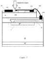
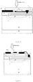
- Figures 5-10 illustrate cross sectional views of the sub pixel of the terahertz detector according to embodiments of the present disclosure.
- FIG 5 shows an embodiment in which the sensitive unit 10 includes graphene material 101.
- a terahertz signal may be incident to a top face of the graphene material directly, or alternatively, the terahertz signal may be focalized by a lens structure and then be passed to the top face of the graphene material, increasing collecting efficiency for the terahertz signal.
- the graphene material 101 is connected in series with the quenching resistor 30, which is formed from a poly silicon material or a highly-resistant material, and the quenching resistor 30 is connected in series with an avalanche photodiode 20 (APD).
- the avalanche photodiode 20 may include a P+ area, an N- area and an N+ area.
- the avalanche photodiode 20 When a positive bias voltage is applied to an electrode at the N+ area and is greater than a breakdown voltage of the avalanche photodiode 20 (APD), the avalanche photodiode 20 (APD) is put into a breakdown state. In common, the bias voltage is greater than the breakdown by 3-5V.
- the area marked by dash line and denoted by number symbol of 21 in Figure 5 is a depletion region.
- the sub pixel of the terahertz detector may further include a passivation layer 50 configured to separate the graphene material 101 from the avalanche photodiode 20.
- the quenching resistor 30 may be surrounded by the passivation layer 50.
- Figure 6 shows an embodiment in which the sensitive unit 10 includes pyroelectricity material 102.
- the embodiment in Figure 6 is similar to that in Figure 5 , except that the sensitive unit 10 includes pyroelectricity material 102.
- a terahertz signal may be incident to a top face of the pyroelectricity material 102 directly.
- a lens may be provided such that terahertz signal may be focalized by the lens and then be passed to the top face of the pyroelectricity material 102, increasing collecting efficiency for the terahertz signal.
- the pyroelectricity material 102 is connected in series with the quenching resistor 30, which is formed from a polysilicon material or a highly-resistant material, and the quenching resistor 30 is connected in series with an avalanche photodiode 20 (APD).
- the quenching resistor 30 is formed from a polysilicon material or a highly-resistant material, and the quenching resistor 30 is connected in series with an avalanche photodiode 20 (APD).
- APD avalanche photodiode 20
- the sub pixel of the terahertz detector may further include a passivation layer 50 configured to separate the pyroelectricity material 102 from the avalanche photodiode 20.
- the quenching resistor 30 may be surrounded by the passivation layer 50.
- FIG 7 shows an embodiment in which the sensitive unit 10 includes a Schottky diode detector 103 (SBD).
- the embodiment in Figure 7 is similar to that in Figure 5 , except that the sensitive unit 10 includes a Schottky diode detector 103 (SBD).
- the Schottky diode detector 103 (SBD) may be made of silicon, or compound semiconductor material 1033 such as gallium arsenide, gallium nitride, silicon carbide.
- the terahertz electromagnetic wave may be incident to a top face of the Schottky diode detector 103 directly.
- a lens may be provided such that terahertz electromagnetic wave may be focalized by the lens and then be passed to the top face of the Schottky diode detector 103, increasing collecting efficiency for the terahertz signal.
- the Schottky diode detector 103 is connected in series with the quenching resistor 30, which is formed from a polysilicon material or a highly-resistant material, and the quenching resistor 30 is connected in series with an avalanche photodiode 20 (APD).
- APD avalanche photodiode 20
- the Schottky diode detector 103 may be directly grown on the structure of the avalanche photodiode 20 and the quenching resistor 30, or alternatively, a Schottky diode detector 103 may be grown separately and then be bonded to the structure of the avalanche photodiode 20 and the quenching resistor 30. Then an electrode of the pixel unit is connected in series with the quenching resistor 30, which is formed from a polysilicon material or a highly-resistant material, by a metal wire.
- the sub pixel of the terahertz detector may further include a passivation layer 50 configured to separate the gallium arsenide/gallium nitride layer 1033 of the Schottky diode detector 103 from the quenching resistor 30, which is formed from a poly silicon material or a highly-resistant material.
- the quenching resistor 30 may be surrounded by the passivation layer 50.
- the Schottky diode detector 103 may include a gallium arsenide (GaAs) layer 1036 at a low concentration dopant, another GaAs layer 1037, a cathode 1032 disposed on the GaAs layer 1036 and an anode 1031 disposed on the GaAs layer 1037 through an ohmic contact, which face the terahertz signal.
- the Schottky diode detector 103 may further include a step on edge at a side face of the Geiger avalanche photodiode 20 and an electrode pad 1034 disposed on the step.
- the anode 1031 of the Schottky diode detector 103 is electrically connected to the electrode pad 1034.
- the Schottky diode detector 103 further includes a GaAs layer (or may be gallium nitride layer) 1033 and the GaAs layer 1036 and the GaAs layer 1037 are disposed on the GaAs layer 1033.
- the electrode pad 1034 is electrically connected to the quenching resistor 30 through a via hole.
- FIG 8 shows an embodiment in which the sensitive unit 10 includes a Schottky diode detector 103 (SBD).
- the Schottky diode detector 103 may be made of silicon, or made of a compound semiconductor material 1033 such as gallium arsenide, gallium nitride, silicon carbide.
- the embodiment in Figure 8 is similar to that in Figure 7 , except that the Schottky diode detector 103 (SBD) is mounted in a reverse manner with relative to the embodiment as shown in Figure 7 , that is, the anode 1031 and the cathode 1032 of the Schottky diode detector 103 face the Geiger avalanche photodiode 20.
- the anode 1031 of the Schottky diode detector 103 is electrically connected to the Geiger avalanche photodiode 20 through the quenching resistor 30. As shown in Figure 8 , the anode 1031 of the Schottky diode detector 103 is directly electrically connected to the quenching resistor 30 through a via hole in the passivation layer 50.
- the terahertz electromagnetic wave may be directly incident to the gallium arsenide/gallium nitride layer 1033 on a back side of the Schottky diode detector 103 and pass through the substrate so as to be collected.
- a lens may be provided such that terahertz electromagnetic wave may be focalized by the lens and then be passed to the gallium arsenide/gallium nitride layer 1033 on the back side of the Schottky diode detector 103 and pass through the substrate so as to be collected, increasing collecting efficiency for the terahertz signal.
- the Schottky diode detector 103 is connected in series with the quenching resistor 30, which is formed from a polysilicon material or a highly-resistant material, and the quenching resistor 30 is connected in series with an avalanche photodiode 20 (APD).
- the Schottky diode detector 103 may be formed separately and provided with electrodes, and then be bonded in an inverted alignment process to the quenching resistor 30 that is grown on the avalanche photodiode 20. Then the other electrode of the Schottky diode detector 103 is led out by a metal wire.
- the sensitive unit 10 is the Schottky diode detector 103.
- the Geiger avalanche photodiode 20 may be formed by a mature silicon process, or may be made of a compound semiconductor material such as gallium arsenide, gallium nitride or silicon nitride, in which the process may be selected and adjusted according to specification, process difficulty and cost.
- the Schottky diode detector 103 may also be formed by a mature silicon process. Therefore, the whole sub pixel may be formed by a mature semiconductor manufacturing process, which may reduce manufacturing cost and increase reliability of a product.
- FIG 9 shows an embodiment in which the sensitive unit 10 is a high-speed electron mobility transistor 104 (HEMT).
- the high-speed electron mobility transistor 104 may be formed by silicon or a compound semiconductor material 1045 such as gallium arsenide, gallium nitride or silicon carbide.
- the terahertz electromagnetic wave may be incident to a top face of the high-speed electron mobility transistor 104 (HEMT) directly.
- a lens may be provided such that terahertz electromagnetic wave may be focalized by the lens and then be passed to the top face of the high-speed electron mobility transistor 104 (HEMT), increasing collecting efficiency for the terahertz signal.
- a gate of the high-speed electron mobility transistor 104 will be controlled individually.
- the high-speed electron mobility transistor 104 When the incident terahertz signal enters the high-speed electron mobility transistor 104 from the gate 1041 and a source electrode 1042, a two dimension electron gas within the high-speed electron mobility transistor 104 is modulated in a self-mixing mode such that an electric signal is outputted from a drain electrode 1043.
- the high-speed electron mobility transistor 104 may be directly grown on the structure of the avalanche photodiode 20 and the quenching resistor 30, or alternatively, a high-speed electron mobility transistor 104 may be grown separately and then be bonded to the structure of the avalanche photodiode 20 and the quenching resistor 30. Then an electrode of the pixel unit is connected in series with the quenching resistor 30, which is formed from a poly silicon material or a highly-resistant material, by a metal wire.
- Figure 10 shows an embodiment in which the sensitive unit 10 is a high-speed electron mobility transistor 104 (HEMT).
- the embodiment of Figure 10 is similar to that in Figure 9 except that the high-speed electron mobility transistor 104 (HEMT) is mounted in a reverse manner with relative to Figure 9 .
- the high-speed electron mobility transistor 104 (HEMT) may be formed by silicon or a compound semiconductor material 1045 such as gallium arsenide, gallium nitride or silicon carbide.
- the terahertz electromagnetic wave may be incident to the compound semiconductor 1045 on a back face of the high-speed electron mobility transistor 104 (HEMT) directly and pass through the substrate so as to be collected.
- a lens may be provided such that terahertz electromagnetic wave may be focalized by the lens and then be incident to the back face of the high-speed electron mobility transistor 104 (HEMT), pass through the substrate so as to be collected, increasing collecting efficiency for the terahertz signal.
- the high-speed electron mobility transistor 104 is connected in series with the quenching resistor 30, which is formed from a polysilicon material or a highly-resistant material, and the quenching resistor 30 is connected in series with an avalanche photodiode 20 (APD).
- the high-speed electron mobility transistor 104 may be formed separately and provided with electrodes, and then be bonded in an inverted alignment process to the quenching resistor 30 that is grown on the avalanche photodiode 20.
- a gate electrode 1041, a source electrode 1042 and a drain electrode 1043 of the high-speed electron mobility transistor 104 face the avalanche photodiode 20.
- the gate electrode 1041 and the source electrode 1042 of the high-speed electron mobility transistor 104 abut against the passivation layer 50 and the drain electrode 1043 of the high-speed electron mobility transistor 104 is electrically connected to the quenching resistor 30 through a via hole in the passivation layer 50.
- the front-end sensitive unit 10 may be any one of the graphene material, the pyroelectricity material, the Schottky diode detector 103, the high-speed electron mobility transistor 104, and other sensitive unit that may directly or indirectly transform the terahertz signal to an electrically signal.
- the sub pixel in the disclosure has a flexible structure and other sensitive unit 10 with a currently new structure may be implemented in the sub pixel.
- the sub pixel in the disclosure may further operate at a low temperature so that an increased sensitivity can be reduced while reducing noise of the avalanche photodiode 20, achieving increased detecting properties as a whole.
- the counting-liked type detection technique is used such that detection efficiency for a terahertz signal is increased while detection precision is increased.
- the operation process of the terahertz detector is as follows: When the pixel unit receives no terahertz signal, the sensitive unit 10 outputs a small and weak signal and thus the Geiger avalanche photodiode 20 (APD) is still in an initial breakdown state under action of a bias voltage; when the sub pixel receives an even very small and weak terahertz signal, the sensitive unit 10 transforms the terahertz signal to an electric signal that can be detected, and the electric signal may be transformed into a voltage signal and applied to the Geiger avalanche photodiode 20 (APD), such that the Geiger avalanche photodiode 20 that is in the initial breakdown state is excited to avalanche, thereby outputting a transient electrical current pulsing signal; when the electrical current increases up to a certain value, a partial potential on the quenching resistor 30 will be increased gradually while a partial potential on the Geiger avalanche photodiode 20 (APD) will be decreased
- Each of the pixel units is formed by a plurality of sub pixels connected in parallel together.
- the value of the outputted signal of a single pixel unit is a resulted value by superimposing electrical current pulsing signals outputted by the plurality of sub pixels under excitation of the terahertz signal and the amplitude of the superimposed electrical current pulsing signals is an integral times of an amplitude of the electrical current pulsing signal outputted by the single sub pixel under excitation of the terahertz signal.
- the pixel unit will output an electrical current pulsing signal having a amplitude of NA.
- the resulting electrical current pulsing signal after having passed the low noise amplifier, is passed to the subsequent read circuit for signal processing. It is shown in practice that the final electrical current pulsing signal obtained in the embodiments is strong and detector sensitivity is high.
Landscapes
- Physics & Mathematics (AREA)
- Spectroscopy & Molecular Physics (AREA)
- General Physics & Mathematics (AREA)
- Health & Medical Sciences (AREA)
- Chemical & Material Sciences (AREA)
- Life Sciences & Earth Sciences (AREA)
- Toxicology (AREA)
- Analytical Chemistry (AREA)
- Biochemistry (AREA)
- General Health & Medical Sciences (AREA)
- Immunology (AREA)
- Pathology (AREA)
- Solid State Image Pick-Up Elements (AREA)
- Light Receiving Elements (AREA)
Abstract
Description
- This application claims the priority benefit of Chinese Patent Application No.
201711499067.4 - Embodiments of the present disclosure relate to detection technical field, and particularly to a terahertz detector.
- Terahertz wave is between a millimeter wave and an infrared wave and thus not only has certain penetration ability like the millimeter wave but also involves a relative high resolving ability like the infrared wave. Thus, the terahertz wave becomes used in security inspection of baggage, package or other items and human body security inspection. Applications of the terahertz wave are developed gradually. However, it is lacked currently to obtain a method of efficiently generating a terahertz wave and an accurate detecting method by using a terahertz wave. A terahertz detector is needed to be studied continuously.
- Detection using a terahertz wave may be classified in technology into two type, i.e., one is coherent detection and the other is non-coherent detection. Due to low outputting power of a terahertz radiation, loss of transfer, heat radiation and noise, et al., a terahertz signal that is detectable is rather weak. Thus, it is in dire need of a terahertz detector with high sensitivity during development of terahertz technology. In the context, many types of terahertz wave detectors are developing. A heat radiation meter is a non-coherent detection that can detect power of a radiation and is not able to report phase information. Further, this type detector commonly works at low temperature in order to reduce detection noise. A pyroelectric transducer has a relative simple structure and operation, and may work in normal temperature. However, a response time of a pyroelectric transducer depends on process of establishing a new balance temperature, that is, a pyroelectric transducer cannot detect a terahertz signal during changing of temperature. A Golay detector has a wide response frequency band, a low equivalent power of noise, a high response sensitivity and may operate at normal temperature. However, the Golay detector is sensitive to vibration and has a bad stability as a whole. In addition, there is a counting type terahertz detector, such as a single electron transistor detector and a quantum cascade laser, which is mainly used to detect photon at a frequency more than 1THz while having not effect for a low energy photon at a frequency less than ITHz. Further, a whole apparatus of counting type terahertz detector is very expensive and is needed to work at super low temperature, and thus is limited to be used widely.
-
-
Figure 1 shows schematic plan views of a planar array structure constituted by a plurality of pixel units and of each of the pixel units according to an embodiment of the present disclosure; -
Figure 2 illustrates an equivalent circuit diagram of a single pixel unit according to an embodiment of the present disclosure; -
Figure 3 shows a work principle view of a single sub pixel of a terahertz detector according to an embodiment of the present disclosure; -
Figure 4 shows a schematic structural view of a pixel unit of a terahertz detector according to an embodiment of the present disclosure; -
Figure 5 shows a schematic structural cross sectional view of a sub pixel according to an embodiment of the present disclosure; -
Figure 6 shows a schematic structural cross sectional view of a sub pixel according to an embodiment of the present disclosure; -
Figure 7 shows a schematic structural cross sectional view of a sub pixel according to an embodiment of the present disclosure; -
Figure 8 shows a schematic structural cross sectional view of a sub pixel according to an embodiment of the present disclosure; -
Figure 9 shows a schematic structural cross sectional view of a sub pixel according to an embodiment of the present disclosure; and -
Figure 10 shows a schematic structural cross sectional view of a sub pixel according to an embodiment of the present disclosure. - While various modifications and replacements may be allowed in the disclosure, embodiments are described and illustrated by reference to examples in the drawings in combination with the following text. However, it is understood that the attached drawings and the following description is not tended to limit the present disclosure to the embodiments, but on the contrary, is tended to cover any modifications equivalent and replacements forms that are fallen into the scope and spirits protected by the attached claims. The drawings are provided to illustrate schematically, instead of being drawn in scale.
- In the text, the terms such as "up", "down" are not intended to limit absolute location of a component, but to make clear where it is located relative to other components. Terms such as "top (side)" and "lower (side)" are used in the text to show a top side or lower side with respect to a vertically-standing object.
- A plurality of embodiments of the present disclosure are described as below.
- Referring to
Figure 1 , schematic plan views of a planar array structure constituted by a plurality of pixel units and of each of the pixel units according to an embodiment of the present disclosure are illustrated.Figure 1 schematically illustrates a relationship between the pixel units and a sub pixel of a counting-liked type terahertz detector according to an embodiment of the present disclosure. InFigure 1 , each of the pixel units may individually provide a signal, like a common image sensor (CMOS) pixel unit or CCD pixel unit. Each of the pixel units of the counting-liked type terahertz detector according to the present embodiment is constituted by a plurality of sub pixels and each of the sub pixels may include no more than one signal trigger configured to transform a terahertz signal to an electrical current pulsing signal and may be a smaller pixel unit, as shown inFigure 1 . The pixel units form a planar array structure and each of the pixel units includes a plurality of sub pixels that may form a planar array structure. - The plurality of sub pixels of each of the pixel units are connected in parallel, that is, an output signal of each of the sub pixels may be superimposed or added together and a result output signal having a superimposed amplitude is represented as a signal of a single pixel unit. In addition, each of the pixel units outputs a signal individually. A single pixel unit includes a number of sub pixels and the number of the sub pixels is adjusted according to requirements of grey gradient or color gradient. In
Figure 1 , the sub pixels in one pixel unit have a color gradients of 16 × 16=256. -
Figure 2 illustrates an equivalent circuit diagram of a single pixel unit of the terahertz detector according to an embodiment of the present disclosure. As shown inFigure 2 , each of the pixel units is formed by a plurality of sub pixels that are connected in parallel. Each of the sub pixels may respectively include a terahertz wavesensitive unit 10, a Geigeravalanche photodiode 20 andquenching resistor 30. It is noted thatFigure 2 merely shows an embodiment of the present disclosure, and in other embodiments, each sub pixel may include other elements. In an embodiment, each sub pixel may include noquenching resistor 30. The sub pixels connected in parallel output a superimposed signal, which obviously is stronger than a signal outputted by any one of the sub pixels. Thus, an enhanced output signal may be obtained. - The terahertz wave
sensitive unit 10 may be a Schottky diode (SBD)detector 103, a high-speed electron mobility transistor 104 (HEMT), a complementary metal oxide semiconductor (CMOS)field effect transistor 104, or may be made of a pyroelectricity material, a graphene material, or may have a structure such as nano-line material, that may transform a terahertz signal to an electric signal. The Geiger avalanche photodiode (APD) 20 may be an avalanche photodiode that is under a breakdown state. In general, an equivalent resistance portion that is made of polysilicon or other highly-resistant material is integrated in an electrode of the Geigeravalanche photodiode 20. - In order to further understand work principle of a single sub pixel,
Figure 3 shows a work principle view of a single sub pixel of a terahertz detector according to an embodiment of the present disclosure. When a sub pixel receives no terahertz signal, thesensitive unit 10 outputs a small and weak signal and thus the Geiger avalanche photodiode 20 (APD) is still in an initial breakdown state under action of a bias voltage. When the sub pixel receives a small and weak terahertz signal, the front-endsensitive unit 10 transforms the terahertz signal to an electric signal and the electric signal may be transformed into a voltage signal and applied to the Geiger avalanche photodiode 20 (APD), such that the Geigeravalanche photodiode 20 that is in the initial breakdown state is excited to avalanche, thereby outputting a transient electrical current pulsing signal. When the electrical current increases up to a certain value, for example up to a certain threshold, a partial potential on thequenching resistor 30 will be increased gradually while a partial potential on theGeiger avalanche photodiode 20 will be decreased gradually and thus theGeiger avalanche photodiode 20 will restore the initial avalanche state. During this, the electrical current pulsing signal outputted by each of the sub pixels due to excitation of the terahertz signal may be considered as a branch signal of a pixel unit. In the embodiment, thesensitive unit 10 located at a front position transforms a weak terahertz signal to an electrical current pulsing signal and the electrical current pulsing signal, after passing through a low noise amplifier, is passed to a subsequent read circuit such that the whole image system is simplified and may directly detect a weak terahertz signal. - In the counting-liked type detector according to an embodiment of the present disclosure, integration of the
sensitive unit 10 located at a front position, theGeiger avalanche photodiode 20 and the quenchingresistor 30 in one sub pixel may further optimize matched impedance of the components, increase a transformation efficiency of signal and increase the whole reliability of the device. - Referring to
Figure 4 , a work process of a single pixel unit of the counting-liked type detector according to an embodiment of the present disclosure is shown. As illustrated in the aboveFigure 3 , a work process of a single sub pixel is described and a single pixel unit is formed by a plurality of sub pixels that are connected in parallel. As a result, a value of an output signal of the pixel unit is resulted from superimposing the electrical current pulsing signals outputted by the sub pixels that are excited by the terahertz signal. The amplitude of the superimposed electrical current pulsing signals is an integral times of an amplitude of the electrical current pulsing signal outputted by the single sub pixel under excitation of the terahertz signal. In other words, if the amplitude of the electrical current pulsing signal outputted by a single sub pixel is A and the pixel unit including N sub pixels is triggered by the terahertz signal, the pixel unit will output an electrical current pulsing signal having a amplitude of NA (assuming electrical current pulsing signals of the sub pixels to be equal to each other). The resulting electrical current pulsing signal, having passed the low noise amplifier, is passed to the subsequent read circuit for signal processing. - It is noted that the sub pixels may respectively output electrical current pulsing signals that are different from one another. For example, in the next text, the sensitive units may be in various types. When the pixel unit includes sensitive units that are the same and have the same specifications, the amplitude of the electrical current pulsing signal outputted by the pixel unit may be NA. If the sensitive units have different specifications, the amplitude of the electrical current pulsing signal outputted by the pixel unit may be a superimposed value of the amplitudes of the electrical current pulsing signals outputted by the sensitive unites. Embodiments of the present disclosure include a plurality of sub pixels that may be formed by various types of sensitive units and form a pixel unit.
- The
sensitive unit 10 located in the front position in the embodiment may be provided with an antenna structure to enhance collection of the terahertz signal. In addition, a size of thesensitive unit 10 may be determined according to a structure and size of the sub pixel. In a situation where space is limited, the antenna structure may be replaced by a super material to enhance collection of the terahertz signal. In an embodiment, thesensitive unit 10 includes an antenna with a microstructure configured to enhance a terahertz signal towards at least one point of thesensitive unit 10. The microstructure of the antenna may be various, such as a staircase structure, a pattern structure. By configuring a suitable microstructure, the antenna may enhance a signal towards one or more points of the antenna when collecting terahertz signal, thereby finally achieving improvement of detecting accuracy. Various embodiments of thesensitive unit 10 are provided herein and however, thesensitive unit 10 in the present disclosure is not limited to the type disclosed herein. -
Figures 5-10 illustrate cross sectional views of the sub pixel of the terahertz detector according to embodiments of the present disclosure. -
Figure 5 shows an embodiment in which thesensitive unit 10 includes graphene material 101. In the embodiment, a terahertz signal may be incident to a top face of the graphene material directly, or alternatively, the terahertz signal may be focalized by a lens structure and then be passed to the top face of the graphene material, increasing collecting efficiency for the terahertz signal. The graphene material 101 is connected in series with the quenchingresistor 30, which is formed from a poly silicon material or a highly-resistant material, and the quenchingresistor 30 is connected in series with an avalanche photodiode 20 (APD). Theavalanche photodiode 20 may include a P+ area, an N- area and an N+ area. When a positive bias voltage is applied to an electrode at the N+ area and is greater than a breakdown voltage of the avalanche photodiode 20 (APD), the avalanche photodiode 20 (APD) is put into a breakdown state. In common, the bias voltage is greater than the breakdown by 3-5V. The area marked by dash line and denoted by number symbol of 21 inFigure 5 is a depletion region. - In the embodiment as shown in
Figure 5 , the sub pixel of the terahertz detector may further include a passivation layer 50 configured to separate the graphene material 101 from theavalanche photodiode 20. The quenchingresistor 30 may be surrounded by the passivation layer 50. -
Figure 6 shows an embodiment in which thesensitive unit 10 includes pyroelectricity material 102. The embodiment inFigure 6 is similar to that inFigure 5 , except that thesensitive unit 10 includes pyroelectricity material 102. In the embodiment, a terahertz signal may be incident to a top face of the pyroelectricity material 102 directly. In an embodiment, a lens may be provided such that terahertz signal may be focalized by the lens and then be passed to the top face of the pyroelectricity material 102, increasing collecting efficiency for the terahertz signal. The pyroelectricity material 102 is connected in series with the quenchingresistor 30, which is formed from a polysilicon material or a highly-resistant material, and the quenchingresistor 30 is connected in series with an avalanche photodiode 20 (APD). - In the embodiment as shown in
Figure 6 , the sub pixel of the terahertz detector may further include a passivation layer 50 configured to separate the pyroelectricity material 102 from theavalanche photodiode 20. The quenchingresistor 30 may be surrounded by the passivation layer 50. -
Figure 7 shows an embodiment in which thesensitive unit 10 includes a Schottky diode detector 103 (SBD). The embodiment inFigure 7 is similar to that inFigure 5 , except that thesensitive unit 10 includes a Schottky diode detector 103 (SBD). The Schottky diode detector 103 (SBD) may be made of silicon, orcompound semiconductor material 1033 such as gallium arsenide, gallium nitride, silicon carbide. The terahertz electromagnetic wave may be incident to a top face of theSchottky diode detector 103 directly. In an embodiment, a lens may be provided such that terahertz electromagnetic wave may be focalized by the lens and then be passed to the top face of theSchottky diode detector 103, increasing collecting efficiency for the terahertz signal. TheSchottky diode detector 103 is connected in series with the quenchingresistor 30, which is formed from a polysilicon material or a highly-resistant material, and the quenchingresistor 30 is connected in series with an avalanche photodiode 20 (APD). Herein, theSchottky diode detector 103 may be directly grown on the structure of theavalanche photodiode 20 and the quenchingresistor 30, or alternatively, aSchottky diode detector 103 may be grown separately and then be bonded to the structure of theavalanche photodiode 20 and the quenchingresistor 30. Then an electrode of the pixel unit is connected in series with the quenchingresistor 30, which is formed from a polysilicon material or a highly-resistant material, by a metal wire. - In the embodiment as shown in
Figure 7 , the sub pixel of the terahertz detector may further include a passivation layer 50 configured to separate the gallium arsenide/gallium nitride layer 1033 of theSchottky diode detector 103 from the quenchingresistor 30, which is formed from a poly silicon material or a highly-resistant material. The quenchingresistor 30 may be surrounded by the passivation layer 50. Specifically, theSchottky diode detector 103 may include a gallium arsenide (GaAs)layer 1036 at a low concentration dopant, anotherGaAs layer 1037, acathode 1032 disposed on theGaAs layer 1036 and ananode 1031 disposed on theGaAs layer 1037 through an ohmic contact, which face the terahertz signal. TheSchottky diode detector 103 may further include a step on edge at a side face of theGeiger avalanche photodiode 20 and anelectrode pad 1034 disposed on the step. Theanode 1031 of theSchottky diode detector 103 is electrically connected to theelectrode pad 1034. TheSchottky diode detector 103 further includes a GaAs layer (or may be gallium nitride layer) 1033 and theGaAs layer 1036 and theGaAs layer 1037 are disposed on theGaAs layer 1033. Theelectrode pad 1034 is electrically connected to the quenchingresistor 30 through a via hole. -
Figure 8 shows an embodiment in which thesensitive unit 10 includes a Schottky diode detector 103 (SBD). The Schottky diode detector 103 (SBD) may be made of silicon, or made of acompound semiconductor material 1033 such as gallium arsenide, gallium nitride, silicon carbide. The embodiment inFigure 8 is similar to that inFigure 7 , except that the Schottky diode detector 103 (SBD) is mounted in a reverse manner with relative to the embodiment as shown inFigure 7 , that is, theanode 1031 and thecathode 1032 of theSchottky diode detector 103 face theGeiger avalanche photodiode 20. Theanode 1031 of theSchottky diode detector 103 is electrically connected to theGeiger avalanche photodiode 20 through the quenchingresistor 30. As shown inFigure 8 , theanode 1031 of theSchottky diode detector 103 is directly electrically connected to the quenchingresistor 30 through a via hole in the passivation layer 50. The terahertz electromagnetic wave may be directly incident to the gallium arsenide/gallium nitride layer 1033 on a back side of theSchottky diode detector 103 and pass through the substrate so as to be collected. In an embodiment, a lens may be provided such that terahertz electromagnetic wave may be focalized by the lens and then be passed to the gallium arsenide/gallium nitride layer 1033 on the back side of theSchottky diode detector 103 and pass through the substrate so as to be collected, increasing collecting efficiency for the terahertz signal. TheSchottky diode detector 103 is connected in series with the quenchingresistor 30, which is formed from a polysilicon material or a highly-resistant material, and the quenchingresistor 30 is connected in series with an avalanche photodiode 20 (APD). Herein, theSchottky diode detector 103 may be formed separately and provided with electrodes, and then be bonded in an inverted alignment process to the quenchingresistor 30 that is grown on theavalanche photodiode 20. Then the other electrode of theSchottky diode detector 103 is led out by a metal wire. - In the embodiments as shown in
Figure 7 andFigure 8 , it is advantage in that thesensitive unit 10 is theSchottky diode detector 103. TheGeiger avalanche photodiode 20 may be formed by a mature silicon process, or may be made of a compound semiconductor material such as gallium arsenide, gallium nitride or silicon nitride, in which the process may be selected and adjusted according to specification, process difficulty and cost. Meanwhile, theSchottky diode detector 103 may also be formed by a mature silicon process. Therefore, the whole sub pixel may be formed by a mature semiconductor manufacturing process, which may reduce manufacturing cost and increase reliability of a product. -
Figure 9 shows an embodiment in which thesensitive unit 10 is a high-speed electron mobility transistor 104 (HEMT). The high-speed electron mobility transistor 104 (HEMT) may be formed by silicon or acompound semiconductor material 1045 such as gallium arsenide, gallium nitride or silicon carbide. The terahertz electromagnetic wave may be incident to a top face of the high-speed electron mobility transistor 104 (HEMT) directly. In an embodiment, a lens may be provided such that terahertz electromagnetic wave may be focalized by the lens and then be passed to the top face of the high-speed electron mobility transistor 104 (HEMT), increasing collecting efficiency for the terahertz signal. A gate of the high-speedelectron mobility transistor 104 will be controlled individually. When the incident terahertz signal enters the high-speedelectron mobility transistor 104 from thegate 1041 and asource electrode 1042, a two dimension electron gas within the high-speedelectron mobility transistor 104 is modulated in a self-mixing mode such that an electric signal is outputted from adrain electrode 1043. Herein, the high-speedelectron mobility transistor 104 may be directly grown on the structure of theavalanche photodiode 20 and the quenchingresistor 30, or alternatively, a high-speedelectron mobility transistor 104 may be grown separately and then be bonded to the structure of theavalanche photodiode 20 and the quenchingresistor 30. Then an electrode of the pixel unit is connected in series with the quenchingresistor 30, which is formed from a poly silicon material or a highly-resistant material, by a metal wire. -
Figure 10 shows an embodiment in which thesensitive unit 10 is a high-speed electron mobility transistor 104 (HEMT). The embodiment ofFigure 10 is similar to that inFigure 9 except that the high-speed electron mobility transistor 104 (HEMT) is mounted in a reverse manner with relative toFigure 9 . The high-speed electron mobility transistor 104 (HEMT) may be formed by silicon or acompound semiconductor material 1045 such as gallium arsenide, gallium nitride or silicon carbide. The terahertz electromagnetic wave may be incident to thecompound semiconductor 1045 on a back face of the high-speed electron mobility transistor 104 (HEMT) directly and pass through the substrate so as to be collected. In an embodiment, a lens may be provided such that terahertz electromagnetic wave may be focalized by the lens and then be incident to the back face of the high-speed electron mobility transistor 104 (HEMT), pass through the substrate so as to be collected, increasing collecting efficiency for the terahertz signal. The high-speedelectron mobility transistor 104 is connected in series with the quenchingresistor 30, which is formed from a polysilicon material or a highly-resistant material, and the quenchingresistor 30 is connected in series with an avalanche photodiode 20 (APD). The high-speedelectron mobility transistor 104 may be formed separately and provided with electrodes, and then be bonded in an inverted alignment process to the quenchingresistor 30 that is grown on theavalanche photodiode 20. Then the other electrode of the high-speedelectron mobility transistor 104 is led out by a metal wire. Specifically, agate electrode 1041, asource electrode 1042 and adrain electrode 1043 of the high-speedelectron mobility transistor 104 face theavalanche photodiode 20. Thegate electrode 1041 and thesource electrode 1042 of the high-speedelectron mobility transistor 104 abut against the passivation layer 50 and thedrain electrode 1043 of the high-speedelectron mobility transistor 104 is electrically connected to the quenchingresistor 30 through a via hole in the passivation layer 50. - In the disclosure, the front-end
sensitive unit 10 may be any one of the graphene material, the pyroelectricity material, theSchottky diode detector 103, the high-speedelectron mobility transistor 104, and other sensitive unit that may directly or indirectly transform the terahertz signal to an electrically signal. The sub pixel in the disclosure has a flexible structure and othersensitive unit 10 with a currently new structure may be implemented in the sub pixel. In addition, the sub pixel in the disclosure may further operate at a low temperature so that an increased sensitivity can be reduced while reducing noise of theavalanche photodiode 20, achieving increased detecting properties as a whole. - In the present disclosure, the counting-liked type detection technique is used such that detection efficiency for a terahertz signal is increased while detection precision is increased.
- In order to assist to understand the terahertz detector according to the embodiments of the present disclosure, an operation process of the terahertz detector is described.
- The operation process of the terahertz detector according to the embodiments is as follows:
When the pixel unit receives no terahertz signal, thesensitive unit 10 outputs a small and weak signal and thus the Geiger avalanche photodiode 20 (APD) is still in an initial breakdown state under action of a bias voltage; when the sub pixel receives an even very small and weak terahertz signal, thesensitive unit 10 transforms the terahertz signal to an electric signal that can be detected, and the electric signal may be transformed into a voltage signal and applied to the Geiger avalanche photodiode 20 (APD), such that theGeiger avalanche photodiode 20 that is in the initial breakdown state is excited to avalanche, thereby outputting a transient electrical current pulsing signal; when the electrical current increases up to a certain value, a partial potential on the quenchingresistor 30 will be increased gradually while a partial potential on the Geiger avalanche photodiode 20 (APD) will be decreased gradually and thus the Geiger avalanche photodiode 20 (APD) will restore the initial avalanche state. During this, the electrical current pulsing signal outputted by each of the sub pixels due to excitation of the terahertz signal may be considered as a sub signal or a branch signal of a pixel unit. - Each of the pixel units is formed by a plurality of sub pixels connected in parallel together. With this configuration, the value of the outputted signal of a single pixel unit is a resulted value by superimposing electrical current pulsing signals outputted by the plurality of sub pixels under excitation of the terahertz signal and the amplitude of the superimposed electrical current pulsing signals is an integral times of an amplitude of the electrical current pulsing signal outputted by the single sub pixel under excitation of the terahertz signal. In other words, if the amplitude of the electrical current pulsing signal outputted by a single sub pixel is A and the pixel unit including N sub pixels is triggered by the terahertz signal, the pixel unit will output an electrical current pulsing signal having a amplitude of NA. The resulting electrical current pulsing signal, after having passed the low noise amplifier, is passed to the subsequent read circuit for signal processing. It is shown in practice that the final electrical current pulsing signal obtained in the embodiments is strong and detector sensitivity is high.
- Although some embodiments according to a general concept of the present disclosure have been revealed and described, it is understood that these embodiments may be modified without departing the principle and spirits of the present disclosure. The scope of the present disclosure is defined by the claims and their equivalents.
Claims (14)
- A terahertz detector comprising a planar array structure that is constituted by a plurality of pixel units, wherein the plurality of pixel units each comprise N sub pixels and each of the sub pixels comprises no more than one signal trigger configured to transform a terahertz signal to an electrical current pulsing signal, and each of the plurality of pixel units detects a signal that is a sum of the electrical current pulsing signals of the N sub pixels, where N is an integer greater than 1.
- The terahertz detector as claimed in claim 1, wherein the N sub pixels of each of the pixel units are connected in parallel.
- The terahertz detector as claimed in claim 1, wherein each of the pixel units comprises:a sensitive unit configured to transform a terahertz signal received to an electrical signal; anda Geiger avalanche photodiode;wherein the sensitive unit is electrically connected to the Geiger avalanche photodiode, and the sub pixel is configured:such that the Geiger avalanche photodiode is in an initial breakdown state under a bias voltage in a case where the sensitive unit receives no terahertz signal, andsuch that in a case where the sensitive unit receives a terahertz signal, the sensitive unit transforms the terahertz signal to an electrical signal that is detectable and the electrical signal is further transformed to a voltage signal and then is applied to the Geiger avalanche photodiode so as to excite the Geiger avalanche photodiode to avalanche and output a transient electrical current pulsing signal.
- The terahertz detector as claimed in claim 3, wherein each of the sub pixel further comprises a quenching resistor, and the sensitive unit, the Geiger avalanche photodiode and the quenching resistor that are connected in series, and
the sub pixel is configured such that: in a case where a value of a electrical current in a circuit in the reaches a threshold value, a partial potential on the quenching resistor increases gradually, a partial potential on the avalanche photodiode decreases gradually and the avalanche photodiode restores to the initial avalanche state. - The terahertz detector as claimed in claim 4, wherein the sensitive unit comprises any one or a combination of more than one of a group consists of a graphene material, a pyroelectricity material, a Schottky diode detector, and a high-speed electron mobility transistor.
- The terahertz detector as claimed in claim 5, wherein the sensitive unit comprises the Schottky diode detector that includes a diode body, and an anode and a cathode disposed on one side of the diode body.
- The terahertz detector as claimed in claim 6, wherein the anode and the cathode of the Schottky diode detector face towards the terahertz signal, the terahertz detector further comprises a step on a surface of the Geiger avalanche photodiode and an electrode pad disposed on the step, and the anode of the Schottky diode detector is electrically connected to the electrode pad; or
wherein the anode and the cathode of the Schottky diode detector face towards the Geiger avalanche photodiode and the anode of the Schottky diode detector is electrically connected to the Geiger avalanche photodiode through the quenching resistor. - The terahertz detector as claimed in claim 5, wherein the sensitive unit comprises the high-speed electron mobility transistor that includes a transistor body and a source electrode, drain electrode and a gate electrode disposed on a side face of the transistor body, wherein the side face of the transistor body of the high-speed electron mobility transistor faces towards the Geiger avalanche photodiode, or a side face, on which the source electrode, the drain electrode and the gate electrode are not disposed, of the transistor body of the high-speed electron mobility transistor faces towards the Geiger avalanche photodiode.
- The terahertz detector as claimed in claim 3, wherein the sensitive unit comprises an antenna having a microstructure configured to enhance a terahertz signal towards at least one point.
- The terahertz detector as claimed in claim 9, wherein the microstructure of the antenna is of a staircase structure, a pattern structure or a super material.
- The terahertz detector as claimed in claim 3, further comprising a sensitive unit lens, through which the terahertz signal passes and impinges on the sensitive unit.
- The terahertz detector as claimed in claim 3, wherein the Geiger avalanche photodiode is made of a semiconductor material including silicon, gallium arsenide, gallium nitride, silicon carbide, graphene or indium phosphide.
- The terahertz detector as claimed in claim 3, further comprising a passivation layer disposed between the sensitive unit and the quenching resistor.
- The terahertz detector as claimed in claim 4, wherein the quenching resistor includes a polysilicon material or other highly-resistant material.
Applications Claiming Priority (1)
| Application Number | Priority Date | Filing Date | Title |
|---|---|---|---|
| CN201711499067.4A CN108007566B (en) | 2017-12-29 | 2017-12-29 | Terahertz detector |
Publications (2)
| Publication Number | Publication Date |
|---|---|
| EP3521783A1 true EP3521783A1 (en) | 2019-08-07 |
| EP3521783B1 EP3521783B1 (en) | 2023-11-15 |
Family
ID=62049839
Family Applications (1)
| Application Number | Title | Priority Date | Filing Date |
|---|---|---|---|
| EP18248030.1A Active EP3521783B1 (en) | 2017-12-29 | 2018-12-27 | Terahertz detector |
Country Status (3)
| Country | Link |
|---|---|
| US (1) | US10775302B2 (en) |
| EP (1) | EP3521783B1 (en) |
| CN (1) | CN108007566B (en) |
Families Citing this family (9)
| Publication number | Priority date | Publication date | Assignee | Title |
|---|---|---|---|---|
| CN108766963A (en) * | 2018-06-01 | 2018-11-06 | 江苏心磁超导体有限公司 | GaN base visualizes Terahertz and detects display chip |
| CN108987383A (en) * | 2018-06-01 | 2018-12-11 | 江苏心磁超导体有限公司 | GaAs base visualizes Terahertz and detects display chip |
| WO2020222149A1 (en) * | 2019-05-02 | 2020-11-05 | Epitronic Holdings Pte. Ltd. | Microelectronic sensor with bolometric or pyroelectric detector for sensing electrical signals in sub-terahertz and terahertz frequency ranges |
| CN111323385B (en) * | 2020-03-03 | 2021-12-28 | 中国科学院物理研究所 | Terahertz camera, terahertz imaging system and application |
| CN112230297B (en) * | 2020-09-03 | 2024-04-09 | 广东工业大学 | Detector based on N×M multi-frequency antenna array and SBD array |
| CN113466166A (en) * | 2021-07-08 | 2021-10-01 | 清华大学 | Gas terahertz spectrum detection system |
| CN113551770B (en) * | 2021-07-23 | 2023-12-29 | 中国科学院半导体研究所 | A terahertz wave amplitude and phase reading device |
| CN113670848B (en) * | 2021-08-23 | 2022-08-02 | 中国人民解放军军事科学院国防科技创新研究院 | High-resolution broadband terahertz detector based on pixelized structure and detection method |
| CN113782644B (en) * | 2021-11-12 | 2022-01-25 | 同方威视技术股份有限公司 | Manufacturing method and detection equipment of terahertz detection device |
Citations (3)
| Publication number | Priority date | Publication date | Assignee | Title |
|---|---|---|---|---|
| WO2008107718A1 (en) * | 2007-03-05 | 2008-09-12 | Sensl Technologies Ltd | Optical position sensitive detector comprising photodiodes operated in geiger-mode |
| KR20150043064A (en) * | 2013-10-14 | 2015-04-22 | 한국전자통신연구원 | Method for manufacturing array-type antenna-coupled detector |
| US20160258807A1 (en) * | 2015-03-06 | 2016-09-08 | Brandt Christopher Pein | Systems, Methods, and Apparatus for Radiation Detection |
Family Cites Families (8)
| Publication number | Priority date | Publication date | Assignee | Title |
|---|---|---|---|---|
| US20040245592A1 (en) * | 2003-05-01 | 2004-12-09 | Yale University | Solid state microchannel plate photodetector |
| US9797779B2 (en) * | 2013-12-05 | 2017-10-24 | National University Of Singapore | Pyroelectric detector using graphene electrode |
| US9851455B2 (en) * | 2014-09-22 | 2017-12-26 | General Electric Company | Solid state photomultiplier with improved pulse shape readout |
| JP6510802B2 (en) * | 2014-12-08 | 2019-05-08 | ローム株式会社 | Terahertz device and method of manufacturing the same |
| JP6486695B2 (en) * | 2015-01-14 | 2019-03-20 | 浜松ホトニクス株式会社 | Bolometer type THz detector |
| CN105333951B (en) * | 2015-11-10 | 2017-11-21 | 中国科学院半导体研究所 | Terahertz wave detector based on field-effect transistor |
| US10571574B1 (en) * | 2016-02-15 | 2020-02-25 | Red Creamery, LLC | Hybrid LADAR with co-planar scanning and imaging field-of-view |
| CN207779553U (en) * | 2017-12-29 | 2018-08-28 | 同方威视技术股份有限公司 | Terahertz detector |
-
2017
- 2017-12-29 CN CN201711499067.4A patent/CN108007566B/en active Active
-
2018
- 2018-12-26 US US16/232,318 patent/US10775302B2/en active Active
- 2018-12-27 EP EP18248030.1A patent/EP3521783B1/en active Active
Patent Citations (3)
| Publication number | Priority date | Publication date | Assignee | Title |
|---|---|---|---|---|
| WO2008107718A1 (en) * | 2007-03-05 | 2008-09-12 | Sensl Technologies Ltd | Optical position sensitive detector comprising photodiodes operated in geiger-mode |
| KR20150043064A (en) * | 2013-10-14 | 2015-04-22 | 한국전자통신연구원 | Method for manufacturing array-type antenna-coupled detector |
| US20160258807A1 (en) * | 2015-03-06 | 2016-09-08 | Brandt Christopher Pein | Systems, Methods, and Apparatus for Radiation Detection |
Non-Patent Citations (1)
| Title |
|---|
| SABAAWI AHMED M A ET AL: "Planar Bowtie Nanoarray for THz Energy Detection", IEEE TRANSACTIONS ON TERAHERTZ SCIENCE AND TECHNOLOGY, IEEE, PISCATAWAY, NJ, USA, vol. 3, no. 5, 1 September 2013 (2013-09-01), pages 524 - 531, XP011527560, ISSN: 2156-342X, [retrieved on 20130920], DOI: 10.1109/TTHZ.2013.2271833 * |
Also Published As
| Publication number | Publication date |
|---|---|
| CN108007566B (en) | 2023-11-03 |
| EP3521783B1 (en) | 2023-11-15 |
| US10775302B2 (en) | 2020-09-15 |
| CN108007566A (en) | 2018-05-08 |
| US20190234870A1 (en) | 2019-08-01 |
Similar Documents
| Publication | Publication Date | Title |
|---|---|---|
| EP3521783B1 (en) | Terahertz detector | |
| US20220069152A1 (en) | Wide-area single-photon detector with time-gating capability | |
| US9007118B2 (en) | Circuit for combining signals | |
| JP6214201B2 (en) | Image acquisition device | |
| US8058618B2 (en) | High sensitivity THz signal detector and camera | |
| CN103148950A (en) | Integrated gating active quenching/restoring circuit | |
| KR20200110782A (en) | Light detection device | |
| Ruggeri et al. | Integrated circuit for subnanosecond gating of InGaAs/InP SPAD | |
| US20110031378A1 (en) | Electromagnetic wave reception device, imaging device, and electromagnetic wave reception method | |
| CN109952649A (en) | Light detection device | |
| Kasjoo et al. | A brief overview of detectors used for terahertz imaging systems | |
| JPH03505390A (en) | Optical radiation detection and processing equipment | |
| JP2011171519A (en) | Schottky type photodetector | |
| Preu et al. | Detection of nanosecond-scale, high power THz pulses with a field effect transistor | |
| CN207779553U (en) | Terahertz detector | |
| US9513212B2 (en) | Photoconductive antenna, camera, imaging device, and measurement device | |
| WO2016143156A1 (en) | Radiation detector and radiation detection device using same | |
| CN111999719A (en) | Single photon TOF image sensor for laser radar | |
| CN112701172A (en) | an avalanche photodiode | |
| EP0002694B1 (en) | Radiation detector | |
| US20150228840A1 (en) | Photoconductive antenna, camera, imaging device, and measurement device | |
| US12490525B2 (en) | Normal-incident photodiode structure with dark current self-compensation function | |
| EP4100704B1 (en) | An integrated photodetecting semiconductor optoelectronic component | |
| Kume et al. | 1.0 THz detection by InAs quantum-well MOSHEMT using GSG THz probe | |
| Elkhatib et al. | Subwavelength detection of terahertz radiation using GaAs HEMTs |
Legal Events
| Date | Code | Title | Description |
|---|---|---|---|
| PUAI | Public reference made under article 153(3) epc to a published international application that has entered the european phase |
Free format text: ORIGINAL CODE: 0009012 |
|
| STAA | Information on the status of an ep patent application or granted ep patent |
Free format text: STATUS: THE APPLICATION HAS BEEN PUBLISHED |
|
| AK | Designated contracting states |
Kind code of ref document: A1 Designated state(s): AL AT BE BG CH CY CZ DE DK EE ES FI FR GB GR HR HU IE IS IT LI LT LU LV MC MK MT NL NO PL PT RO RS SE SI SK SM TR |
|
| AX | Request for extension of the european patent |
Extension state: BA ME |
|
| STAA | Information on the status of an ep patent application or granted ep patent |
Free format text: STATUS: REQUEST FOR EXAMINATION WAS MADE |
|
| 17P | Request for examination filed |
Effective date: 20200205 |
|
| RBV | Designated contracting states (corrected) |
Designated state(s): AL AT BE BG CH CY CZ DE DK EE ES FI FR GB GR HR HU IE IS IT LI LT LU LV MC MK MT NL NO PL PT RO RS SE SI SK SM TR |
|
| STAA | Information on the status of an ep patent application or granted ep patent |
Free format text: STATUS: EXAMINATION IS IN PROGRESS |
|
| 17Q | First examination report despatched |
Effective date: 20220103 |
|
| GRAP | Despatch of communication of intention to grant a patent |
Free format text: ORIGINAL CODE: EPIDOSNIGR1 |
|
| STAA | Information on the status of an ep patent application or granted ep patent |
Free format text: STATUS: GRANT OF PATENT IS INTENDED |
|
| INTG | Intention to grant announced |
Effective date: 20230831 |
|
| GRAS | Grant fee paid |
Free format text: ORIGINAL CODE: EPIDOSNIGR3 |
|
| GRAA | (expected) grant |
Free format text: ORIGINAL CODE: 0009210 |
|
| STAA | Information on the status of an ep patent application or granted ep patent |
Free format text: STATUS: THE PATENT HAS BEEN GRANTED |
|
| AK | Designated contracting states |
Kind code of ref document: B1 Designated state(s): AL AT BE BG CH CY CZ DE DK EE ES FI FR GB GR HR HU IE IS IT LI LT LU LV MC MK MT NL NO PL PT RO RS SE SI SK SM TR |
|
| REG | Reference to a national code |
Ref country code: CH Ref legal event code: EP Ref country code: GB Ref legal event code: FG4D |
|
| REG | Reference to a national code |
Ref country code: DE Ref legal event code: R096 Ref document number: 602018061069 Country of ref document: DE |
|
| REG | Reference to a national code |
Ref country code: IE Ref legal event code: FG4D |
|
| P01 | Opt-out of the competence of the unified patent court (upc) registered |
Effective date: 20231208 |
|
| REG | Reference to a national code |
Ref country code: LT Ref legal event code: MG9D |
|
| REG | Reference to a national code |
Ref country code: NL Ref legal event code: MP Effective date: 20231115 |
|
| PG25 | Lapsed in a contracting state [announced via postgrant information from national office to epo] |
Ref country code: GR Free format text: LAPSE BECAUSE OF FAILURE TO SUBMIT A TRANSLATION OF THE DESCRIPTION OR TO PAY THE FEE WITHIN THE PRESCRIBED TIME-LIMIT Effective date: 20240216 |
|
| PG25 | Lapsed in a contracting state [announced via postgrant information from national office to epo] |
Ref country code: IS Free format text: LAPSE BECAUSE OF FAILURE TO SUBMIT A TRANSLATION OF THE DESCRIPTION OR TO PAY THE FEE WITHIN THE PRESCRIBED TIME-LIMIT Effective date: 20240315 |
|
| PG25 | Lapsed in a contracting state [announced via postgrant information from national office to epo] |
Ref country code: LT Free format text: LAPSE BECAUSE OF FAILURE TO SUBMIT A TRANSLATION OF THE DESCRIPTION OR TO PAY THE FEE WITHIN THE PRESCRIBED TIME-LIMIT Effective date: 20231115 |
|
| REG | Reference to a national code |
Ref country code: AT Ref legal event code: MK05 Ref document number: 1632171 Country of ref document: AT Kind code of ref document: T Effective date: 20231115 |
|
| PG25 | Lapsed in a contracting state [announced via postgrant information from national office to epo] |
Ref country code: NL Free format text: LAPSE BECAUSE OF FAILURE TO SUBMIT A TRANSLATION OF THE DESCRIPTION OR TO PAY THE FEE WITHIN THE PRESCRIBED TIME-LIMIT Effective date: 20231115 |
|
| PG25 | Lapsed in a contracting state [announced via postgrant information from national office to epo] |
Ref country code: AT Free format text: LAPSE BECAUSE OF FAILURE TO SUBMIT A TRANSLATION OF THE DESCRIPTION OR TO PAY THE FEE WITHIN THE PRESCRIBED TIME-LIMIT Effective date: 20231115 |
|
| PG25 | Lapsed in a contracting state [announced via postgrant information from national office to epo] |
Ref country code: ES Free format text: LAPSE BECAUSE OF FAILURE TO SUBMIT A TRANSLATION OF THE DESCRIPTION OR TO PAY THE FEE WITHIN THE PRESCRIBED TIME-LIMIT Effective date: 20231115 |
|
| PG25 | Lapsed in a contracting state [announced via postgrant information from national office to epo] |
Ref country code: NL Free format text: LAPSE BECAUSE OF FAILURE TO SUBMIT A TRANSLATION OF THE DESCRIPTION OR TO PAY THE FEE WITHIN THE PRESCRIBED TIME-LIMIT Effective date: 20231115 Ref country code: LT Free format text: LAPSE BECAUSE OF FAILURE TO SUBMIT A TRANSLATION OF THE DESCRIPTION OR TO PAY THE FEE WITHIN THE PRESCRIBED TIME-LIMIT Effective date: 20231115 Ref country code: IS Free format text: LAPSE BECAUSE OF FAILURE TO SUBMIT A TRANSLATION OF THE DESCRIPTION OR TO PAY THE FEE WITHIN THE PRESCRIBED TIME-LIMIT Effective date: 20240315 Ref country code: GR Free format text: LAPSE BECAUSE OF FAILURE TO SUBMIT A TRANSLATION OF THE DESCRIPTION OR TO PAY THE FEE WITHIN THE PRESCRIBED TIME-LIMIT Effective date: 20240216 Ref country code: ES Free format text: LAPSE BECAUSE OF FAILURE TO SUBMIT A TRANSLATION OF THE DESCRIPTION OR TO PAY THE FEE WITHIN THE PRESCRIBED TIME-LIMIT Effective date: 20231115 Ref country code: BG Free format text: LAPSE BECAUSE OF FAILURE TO SUBMIT A TRANSLATION OF THE DESCRIPTION OR TO PAY THE FEE WITHIN THE PRESCRIBED TIME-LIMIT Effective date: 20240215 Ref country code: AT Free format text: LAPSE BECAUSE OF FAILURE TO SUBMIT A TRANSLATION OF THE DESCRIPTION OR TO PAY THE FEE WITHIN THE PRESCRIBED TIME-LIMIT Effective date: 20231115 Ref country code: PT Free format text: LAPSE BECAUSE OF FAILURE TO SUBMIT A TRANSLATION OF THE DESCRIPTION OR TO PAY THE FEE WITHIN THE PRESCRIBED TIME-LIMIT Effective date: 20240315 |
|
| PG25 | Lapsed in a contracting state [announced via postgrant information from national office to epo] |
Ref country code: SE Free format text: LAPSE BECAUSE OF FAILURE TO SUBMIT A TRANSLATION OF THE DESCRIPTION OR TO PAY THE FEE WITHIN THE PRESCRIBED TIME-LIMIT Effective date: 20231115 Ref country code: RS Free format text: LAPSE BECAUSE OF FAILURE TO SUBMIT A TRANSLATION OF THE DESCRIPTION OR TO PAY THE FEE WITHIN THE PRESCRIBED TIME-LIMIT Effective date: 20231115 Ref country code: PL Free format text: LAPSE BECAUSE OF FAILURE TO SUBMIT A TRANSLATION OF THE DESCRIPTION OR TO PAY THE FEE WITHIN THE PRESCRIBED TIME-LIMIT Effective date: 20231115 Ref country code: NO Free format text: LAPSE BECAUSE OF FAILURE TO SUBMIT A TRANSLATION OF THE DESCRIPTION OR TO PAY THE FEE WITHIN THE PRESCRIBED TIME-LIMIT Effective date: 20240215 Ref country code: LV Free format text: LAPSE BECAUSE OF FAILURE TO SUBMIT A TRANSLATION OF THE DESCRIPTION OR TO PAY THE FEE WITHIN THE PRESCRIBED TIME-LIMIT Effective date: 20231115 Ref country code: HR Free format text: LAPSE BECAUSE OF FAILURE TO SUBMIT A TRANSLATION OF THE DESCRIPTION OR TO PAY THE FEE WITHIN THE PRESCRIBED TIME-LIMIT Effective date: 20231115 |
|
| PG25 | Lapsed in a contracting state [announced via postgrant information from national office to epo] |
Ref country code: DK Free format text: LAPSE BECAUSE OF FAILURE TO SUBMIT A TRANSLATION OF THE DESCRIPTION OR TO PAY THE FEE WITHIN THE PRESCRIBED TIME-LIMIT Effective date: 20231115 |
|
| PG25 | Lapsed in a contracting state [announced via postgrant information from national office to epo] |
Ref country code: CZ Free format text: LAPSE BECAUSE OF FAILURE TO SUBMIT A TRANSLATION OF THE DESCRIPTION OR TO PAY THE FEE WITHIN THE PRESCRIBED TIME-LIMIT Effective date: 20231115 |
|
| PG25 | Lapsed in a contracting state [announced via postgrant information from national office to epo] |
Ref country code: SK Free format text: LAPSE BECAUSE OF FAILURE TO SUBMIT A TRANSLATION OF THE DESCRIPTION OR TO PAY THE FEE WITHIN THE PRESCRIBED TIME-LIMIT Effective date: 20231115 |
|
| PG25 | Lapsed in a contracting state [announced via postgrant information from national office to epo] |
Ref country code: SM Free format text: LAPSE BECAUSE OF FAILURE TO SUBMIT A TRANSLATION OF THE DESCRIPTION OR TO PAY THE FEE WITHIN THE PRESCRIBED TIME-LIMIT Effective date: 20231115 Ref country code: SK Free format text: LAPSE BECAUSE OF FAILURE TO SUBMIT A TRANSLATION OF THE DESCRIPTION OR TO PAY THE FEE WITHIN THE PRESCRIBED TIME-LIMIT Effective date: 20231115 Ref country code: RO Free format text: LAPSE BECAUSE OF FAILURE TO SUBMIT A TRANSLATION OF THE DESCRIPTION OR TO PAY THE FEE WITHIN THE PRESCRIBED TIME-LIMIT Effective date: 20231115 Ref country code: IT Free format text: LAPSE BECAUSE OF FAILURE TO SUBMIT A TRANSLATION OF THE DESCRIPTION OR TO PAY THE FEE WITHIN THE PRESCRIBED TIME-LIMIT Effective date: 20231115 Ref country code: EE Free format text: LAPSE BECAUSE OF FAILURE TO SUBMIT A TRANSLATION OF THE DESCRIPTION OR TO PAY THE FEE WITHIN THE PRESCRIBED TIME-LIMIT Effective date: 20231115 Ref country code: DK Free format text: LAPSE BECAUSE OF FAILURE TO SUBMIT A TRANSLATION OF THE DESCRIPTION OR TO PAY THE FEE WITHIN THE PRESCRIBED TIME-LIMIT Effective date: 20231115 Ref country code: CZ Free format text: LAPSE BECAUSE OF FAILURE TO SUBMIT A TRANSLATION OF THE DESCRIPTION OR TO PAY THE FEE WITHIN THE PRESCRIBED TIME-LIMIT Effective date: 20231115 |
|
| REG | Reference to a national code |
Ref country code: CH Ref legal event code: PL |
|
| REG | Reference to a national code |
Ref country code: DE Ref legal event code: R097 Ref document number: 602018061069 Country of ref document: DE |
|
| PG25 | Lapsed in a contracting state [announced via postgrant information from national office to epo] |
Ref country code: LU Free format text: LAPSE BECAUSE OF NON-PAYMENT OF DUE FEES Effective date: 20231227 |
|
| PG25 | Lapsed in a contracting state [announced via postgrant information from national office to epo] |
Ref country code: MC Free format text: LAPSE BECAUSE OF FAILURE TO SUBMIT A TRANSLATION OF THE DESCRIPTION OR TO PAY THE FEE WITHIN THE PRESCRIBED TIME-LIMIT Effective date: 20231115 |
|
| REG | Reference to a national code |
Ref country code: BE Ref legal event code: MM Effective date: 20231231 |
|
| PG25 | Lapsed in a contracting state [announced via postgrant information from national office to epo] |
Ref country code: MC Free format text: LAPSE BECAUSE OF FAILURE TO SUBMIT A TRANSLATION OF THE DESCRIPTION OR TO PAY THE FEE WITHIN THE PRESCRIBED TIME-LIMIT Effective date: 20231115 Ref country code: LU Free format text: LAPSE BECAUSE OF NON-PAYMENT OF DUE FEES Effective date: 20231227 |
|
| PLBE | No opposition filed within time limit |
Free format text: ORIGINAL CODE: 0009261 |
|
| STAA | Information on the status of an ep patent application or granted ep patent |
Free format text: STATUS: NO OPPOSITION FILED WITHIN TIME LIMIT |
|
| REG | Reference to a national code |
Ref country code: IE Ref legal event code: MM4A |
|
| PG25 | Lapsed in a contracting state [announced via postgrant information from national office to epo] |
Ref country code: IE Free format text: LAPSE BECAUSE OF NON-PAYMENT OF DUE FEES Effective date: 20231227 |
|
| PG25 | Lapsed in a contracting state [announced via postgrant information from national office to epo] |
Ref country code: BE Free format text: LAPSE BECAUSE OF NON-PAYMENT OF DUE FEES Effective date: 20231231 |
|
| PG25 | Lapsed in a contracting state [announced via postgrant information from national office to epo] |
Ref country code: FR Free format text: LAPSE BECAUSE OF NON-PAYMENT OF DUE FEES Effective date: 20240115 |
|
| PG25 | Lapsed in a contracting state [announced via postgrant information from national office to epo] |
Ref country code: CH Free format text: LAPSE BECAUSE OF NON-PAYMENT OF DUE FEES Effective date: 20231231 |
|
| 26N | No opposition filed |
Effective date: 20240819 |
|
| PG25 | Lapsed in a contracting state [announced via postgrant information from national office to epo] |
Ref country code: SI Free format text: LAPSE BECAUSE OF FAILURE TO SUBMIT A TRANSLATION OF THE DESCRIPTION OR TO PAY THE FEE WITHIN THE PRESCRIBED TIME-LIMIT Effective date: 20231115 |
|
| PG25 | Lapsed in a contracting state [announced via postgrant information from national office to epo] |
Ref country code: SI Free format text: LAPSE BECAUSE OF FAILURE TO SUBMIT A TRANSLATION OF THE DESCRIPTION OR TO PAY THE FEE WITHIN THE PRESCRIBED TIME-LIMIT Effective date: 20231115 Ref country code: IE Free format text: LAPSE BECAUSE OF NON-PAYMENT OF DUE FEES Effective date: 20231227 Ref country code: FR Free format text: LAPSE BECAUSE OF NON-PAYMENT OF DUE FEES Effective date: 20240115 Ref country code: CH Free format text: LAPSE BECAUSE OF NON-PAYMENT OF DUE FEES Effective date: 20231231 Ref country code: BE Free format text: LAPSE BECAUSE OF NON-PAYMENT OF DUE FEES Effective date: 20231231 |
|
| PG25 | Lapsed in a contracting state [announced via postgrant information from national office to epo] |
Ref country code: FI Free format text: LAPSE BECAUSE OF FAILURE TO SUBMIT A TRANSLATION OF THE DESCRIPTION OR TO PAY THE FEE WITHIN THE PRESCRIBED TIME-LIMIT Effective date: 20231115 |
|
| PG25 | Lapsed in a contracting state [announced via postgrant information from national office to epo] |
Ref country code: CY Free format text: LAPSE BECAUSE OF FAILURE TO SUBMIT A TRANSLATION OF THE DESCRIPTION OR TO PAY THE FEE WITHIN THE PRESCRIBED TIME-LIMIT; INVALID AB INITIO Effective date: 20181227 |
|
| PG25 | Lapsed in a contracting state [announced via postgrant information from national office to epo] |
Ref country code: HU Free format text: LAPSE BECAUSE OF FAILURE TO SUBMIT A TRANSLATION OF THE DESCRIPTION OR TO PAY THE FEE WITHIN THE PRESCRIBED TIME-LIMIT; INVALID AB INITIO Effective date: 20181227 |
|
| PG25 | Lapsed in a contracting state [announced via postgrant information from national office to epo] |
Ref country code: TR Free format text: LAPSE BECAUSE OF FAILURE TO SUBMIT A TRANSLATION OF THE DESCRIPTION OR TO PAY THE FEE WITHIN THE PRESCRIBED TIME-LIMIT Effective date: 20231115 |
|
| PGFP | Annual fee paid to national office [announced via postgrant information from national office to epo] |
Ref country code: GB Payment date: 20251111 Year of fee payment: 8 |
|
| PGFP | Annual fee paid to national office [announced via postgrant information from national office to epo] |
Ref country code: DE Payment date: 20251222 Year of fee payment: 8 |