EP3516526B1 - Memory management supporting huge pages - Google Patents
Memory management supporting huge pages Download PDFInfo
- Publication number
- EP3516526B1 EP3516526B1 EP17761767.7A EP17761767A EP3516526B1 EP 3516526 B1 EP3516526 B1 EP 3516526B1 EP 17761767 A EP17761767 A EP 17761767A EP 3516526 B1 EP3516526 B1 EP 3516526B1
- Authority
- EP
- European Patent Office
- Prior art keywords
- page
- data
- memory
- main memory
- pages
- Prior art date
- Legal status (The legal status is an assumption and is not a legal conclusion. Google has not performed a legal analysis and makes no representation as to the accuracy of the status listed.)
- Active
Links
Images

Classifications
-
- G—PHYSICS
- G06—COMPUTING OR CALCULATING; COUNTING
- G06F—ELECTRIC DIGITAL DATA PROCESSING
- G06F12/00—Accessing, addressing or allocating within memory systems or architectures
- G06F12/02—Addressing or allocation; Relocation
- G06F12/08—Addressing or allocation; Relocation in hierarchically structured memory systems, e.g. virtual memory systems
- G06F12/0802—Addressing of a memory level in which the access to the desired data or data block requires associative addressing means, e.g. caches
- G06F12/0866—Addressing of a memory level in which the access to the desired data or data block requires associative addressing means, e.g. caches for peripheral storage systems, e.g. disk cache
- G06F12/0873—Mapping of cache memory to specific storage devices or parts thereof
-
- G—PHYSICS
- G06—COMPUTING OR CALCULATING; COUNTING
- G06F—ELECTRIC DIGITAL DATA PROCESSING
- G06F12/00—Accessing, addressing or allocating within memory systems or architectures
- G06F12/02—Addressing or allocation; Relocation
- G06F12/0223—User address space allocation, e.g. contiguous or non contiguous base addressing
- G06F12/023—Free address space management
-
- G—PHYSICS
- G06—COMPUTING OR CALCULATING; COUNTING
- G06F—ELECTRIC DIGITAL DATA PROCESSING
- G06F12/00—Accessing, addressing or allocating within memory systems or architectures
- G06F12/02—Addressing or allocation; Relocation
- G06F12/04—Addressing variable-length words or parts of words
-
- G—PHYSICS
- G06—COMPUTING OR CALCULATING; COUNTING
- G06F—ELECTRIC DIGITAL DATA PROCESSING
- G06F12/00—Accessing, addressing or allocating within memory systems or architectures
- G06F12/02—Addressing or allocation; Relocation
- G06F12/08—Addressing or allocation; Relocation in hierarchically structured memory systems, e.g. virtual memory systems
- G06F12/0802—Addressing of a memory level in which the access to the desired data or data block requires associative addressing means, e.g. caches
- G06F12/0866—Addressing of a memory level in which the access to the desired data or data block requires associative addressing means, e.g. caches for peripheral storage systems, e.g. disk cache
- G06F12/0868—Data transfer between cache memory and other subsystems, e.g. storage devices or host systems
-
- G—PHYSICS
- G06—COMPUTING OR CALCULATING; COUNTING
- G06F—ELECTRIC DIGITAL DATA PROCESSING
- G06F12/00—Accessing, addressing or allocating within memory systems or architectures
- G06F12/02—Addressing or allocation; Relocation
- G06F12/08—Addressing or allocation; Relocation in hierarchically structured memory systems, e.g. virtual memory systems
- G06F12/0802—Addressing of a memory level in which the access to the desired data or data block requires associative addressing means, e.g. caches
- G06F12/0866—Addressing of a memory level in which the access to the desired data or data block requires associative addressing means, e.g. caches for peripheral storage systems, e.g. disk cache
- G06F12/0871—Allocation or management of cache space
-
- G—PHYSICS
- G06—COMPUTING OR CALCULATING; COUNTING
- G06F—ELECTRIC DIGITAL DATA PROCESSING
- G06F12/00—Accessing, addressing or allocating within memory systems or architectures
- G06F12/02—Addressing or allocation; Relocation
- G06F12/08—Addressing or allocation; Relocation in hierarchically structured memory systems, e.g. virtual memory systems
- G06F12/0802—Addressing of a memory level in which the access to the desired data or data block requires associative addressing means, e.g. caches
- G06F12/0877—Cache access modes
- G06F12/0882—Page mode
-
- G—PHYSICS
- G06—COMPUTING OR CALCULATING; COUNTING
- G06F—ELECTRIC DIGITAL DATA PROCESSING
- G06F12/00—Accessing, addressing or allocating within memory systems or architectures
- G06F12/02—Addressing or allocation; Relocation
- G06F12/08—Addressing or allocation; Relocation in hierarchically structured memory systems, e.g. virtual memory systems
- G06F12/0802—Addressing of a memory level in which the access to the desired data or data block requires associative addressing means, e.g. caches
- G06F12/0893—Caches characterised by their organisation or structure
- G06F12/0897—Caches characterised by their organisation or structure with two or more cache hierarchy levels
-
- G—PHYSICS
- G06—COMPUTING OR CALCULATING; COUNTING
- G06F—ELECTRIC DIGITAL DATA PROCESSING
- G06F12/00—Accessing, addressing or allocating within memory systems or architectures
- G06F12/02—Addressing or allocation; Relocation
- G06F12/08—Addressing or allocation; Relocation in hierarchically structured memory systems, e.g. virtual memory systems
- G06F12/10—Address translation
- G06F12/1009—Address translation using page tables, e.g. page table structures
-
- G—PHYSICS
- G06—COMPUTING OR CALCULATING; COUNTING
- G06F—ELECTRIC DIGITAL DATA PROCESSING
- G06F12/00—Accessing, addressing or allocating within memory systems or architectures
- G06F12/02—Addressing or allocation; Relocation
- G06F12/08—Addressing or allocation; Relocation in hierarchically structured memory systems, e.g. virtual memory systems
- G06F12/10—Address translation
- G06F12/1027—Address translation using associative or pseudo-associative address translation means, e.g. translation look-aside buffer [TLB]
-
- G—PHYSICS
- G06—COMPUTING OR CALCULATING; COUNTING
- G06F—ELECTRIC DIGITAL DATA PROCESSING
- G06F12/00—Accessing, addressing or allocating within memory systems or architectures
- G06F12/02—Addressing or allocation; Relocation
- G06F12/08—Addressing or allocation; Relocation in hierarchically structured memory systems, e.g. virtual memory systems
- G06F12/12—Replacement control
-
- G—PHYSICS
- G06—COMPUTING OR CALCULATING; COUNTING
- G06F—ELECTRIC DIGITAL DATA PROCESSING
- G06F12/00—Accessing, addressing or allocating within memory systems or architectures
- G06F12/02—Addressing or allocation; Relocation
- G06F12/08—Addressing or allocation; Relocation in hierarchically structured memory systems, e.g. virtual memory systems
- G06F12/0802—Addressing of a memory level in which the access to the desired data or data block requires associative addressing means, e.g. caches
- G06F12/0806—Multiuser, multiprocessor or multiprocessing cache systems
- G06F12/0815—Cache consistency protocols
-
- G—PHYSICS
- G06—COMPUTING OR CALCULATING; COUNTING
- G06F—ELECTRIC DIGITAL DATA PROCESSING
- G06F2212/00—Indexing scheme relating to accessing, addressing or allocation within memory systems or architectures
- G06F2212/10—Providing a specific technical effect
- G06F2212/1016—Performance improvement
- G06F2212/1024—Latency reduction
-
- G—PHYSICS
- G06—COMPUTING OR CALCULATING; COUNTING
- G06F—ELECTRIC DIGITAL DATA PROCESSING
- G06F2212/00—Indexing scheme relating to accessing, addressing or allocation within memory systems or architectures
- G06F2212/15—Use in a specific computing environment
- G06F2212/152—Virtualized environment, e.g. logically partitioned system
-
- G—PHYSICS
- G06—COMPUTING OR CALCULATING; COUNTING
- G06F—ELECTRIC DIGITAL DATA PROCESSING
- G06F2212/00—Indexing scheme relating to accessing, addressing or allocation within memory systems or architectures
- G06F2212/30—Providing cache or TLB in specific location of a processing system
- G06F2212/304—In main memory subsystem
- G06F2212/3042—In main memory subsystem being part of a memory device, e.g. cache DRAM
-
- G—PHYSICS
- G06—COMPUTING OR CALCULATING; COUNTING
- G06F—ELECTRIC DIGITAL DATA PROCESSING
- G06F2212/00—Indexing scheme relating to accessing, addressing or allocation within memory systems or architectures
- G06F2212/30—Providing cache or TLB in specific location of a processing system
- G06F2212/305—Providing cache or TLB in specific location of a processing system being part of a memory device, e.g. cache DRAM
-
- G—PHYSICS
- G06—COMPUTING OR CALCULATING; COUNTING
- G06F—ELECTRIC DIGITAL DATA PROCESSING
- G06F2212/00—Indexing scheme relating to accessing, addressing or allocation within memory systems or architectures
- G06F2212/60—Details of cache memory
- G06F2212/604—Details relating to cache allocation
-
- G—PHYSICS
- G06—COMPUTING OR CALCULATING; COUNTING
- G06F—ELECTRIC DIGITAL DATA PROCESSING
- G06F2212/00—Indexing scheme relating to accessing, addressing or allocation within memory systems or architectures
- G06F2212/65—Details of virtual memory and virtual address translation
- G06F2212/652—Page size control
Definitions
- the present specification generally relates to memory systems.
- DRAM Dynamic Random Access Memory
- US2009172344 (A1 ) describes that a method, system, and apparatus may initialize a fixed plurality of page table entries for a fixed plurality of pages in memory, each page having a first size, wherein a linear address for each page table entry corresponds to a physical address and the fixed plurality of pages are aligned.
- a bit in each of the page table entries for the aligned pages may be set to indicate whether or not the fixed plurality of pages is to be treated as one combined page having a second page size larger than the first page size.
- WO2011002900 (A1 ) describes a processor including a virtual memory paging mechanism.
- the virtual memory paging mechanism enables an operating system operating on the processor to use pages of a first size and a second size, the second size being greater than the first size.
- the mechanism further enables the operating system to use superpages including two or more contiguous pages of the first size.
- the size of a superpage is less than the second size.
- the processor further includes a page table having a separate entry for each of the pages included in each superpage. The operating system accesses each superpage using a single virtual address.
- the mechanism interprets a single entry in a translation lookaside buffer TLB as referring to a region of memory comprising a set of pages that correspond to a superpage in response to detecting a superpage enable indicator associated with the entry in the TLB is asserted.
- a second tier of memory may be used, such as disk-based memory, NAND flash memory, spin torque transfer magnetic memory (STT-MRAM), resistive random access memory (ReRAM), or the like.
- the second tier of memory may be accessed locally over a memory or IO bus, or remotely over a high-speed network.
- applications need to explicitly manage data placement or the system must provide automatic management that transparently moves data between memory tiers.
- huge pages or large pages or super pages have been shown to provide a significant performance increase for most workloads and particularly for cloud-based serving applications, where huge pages are blocks of memory that are larger in size, e.g., 8KB, 64KB, 256KB, 1MB, 2MB, 4MB, 16MB, 256MB, 512MB, or 1GB, than atypical page, which may be 4KB, depending on processor architecture.
- new techniques are needed for automatic management with minimal performance impact to overcome the inadequacies of existing techniques.
- One innovative aspect of the subject matter described in this specification is embodied in systems and methods that include receiving a request to access, from a main memory, data contained in a first portion of a first page of data, the first page of data having a first page size and the first portion comprising a second page size that is less than the first page size; initiating a page fault based on determining that the first page of data is not stored in the main memory and is stored in a secondary memory; in response to initiating the page fault, allocating a portion of the main memory equivalent to the first page size; transferring the first portion of the first page of data from the secondary memory to the allocated portion of the main memory without transferring the entire first page of data, wherein a remaining amount of the first page of data remains stored in the secondary memory; and updating a first page table entry associated with the first portion of the first page of data to point to a location of the allocated portion of the main memory to which the first portion of the first page of data is transferred.
- the remaining amount of the first page of data is transferred from the secondary memory to the main memory. Transferring the remaining amount of the first page of data may include repeatedly transferring respective portions, corresponding to the second page size, of the first page of data from the secondary memory to the allocated portion of the main memory until the entire first page of data is stored in the main memory; and updating a respective page table entry for each of the respective portions of the first page of data to point to respective locations of the respective portions of the first page of data in the main memory.
- the first page of data is reassembled from the respective portions of the first page of data transferred from the secondary memory to the allocated portion of the main memory; and a page table entry associated with the first page of data is updated to point to a location of the reassembled first page of data in the main memory.
- Another aspect of the subject matter described in this specification is embodied in systems and methods that include, before transferring the remaining portion of the first page of data from the secondary memory to the main memory, indicating that the first portion of the first page of data that was requested to be accessed has been transferred to the main memory.
- Another innovative aspect of the subject matter described in this specification is embodied in systems and methods that include determining whether an access bit is set for each page table entry of a page table based on a scan of the page table with a page table scanner, the access bit indicating whether a page associated with the page table entry was accessed in a last scan period, wherein at least one of the pages having the first page size is divided into pages of the second page size with a page table entry for each of the pages of the second page size in the page table being scanned; incrementing a count for each page in response to determining that the access bit is not set for the page table entry associated with the page; and after determining whether the access bit is set for each page table entry, resetting the access bit.
- one of a least used pages having the first page size is determined based on the count for each page and releasing the one of the least used pages into the secondary memory, and a portion of the main memory equivalent to the first page size is allocated at the location of the released one of the least used pages; and if the portion of the main memory equivalent to the first page size can be allocated, the first portion of the first page of data is transferred from the secondary memory to the allocated portion of the main memory.
- the usage or access statistics for pages in memory may be more precise and accurate than current methods involving software and sampling techniques because access statistics may be determined at the sub-page level rather than just at the page level.
- the delay caused by transferring a page in response to a request to access the page may be reduced, which may result in faster execution of the application or process being executed.
- Another advantage is that the system can take advantage of the benefits of huge pages, such as better memory access performance due to fewer levels of page tables and better translation lookaside buffer (TLB) coverage, and still perform paging at a small page granularity, which provides better page fault performance due to the reduced latency of servicing a page fault that only needs to transfer a small page. Therefore, both the memory access benefits of huge pages and the demand paging benefits of small pages can both be achieved. Moreover, only the data that is needed may be transferred according to the small page size, and as a result, the main memory is not occupied with unnecessary data, due to better maintaining hot data in main memory and cold data in secondary memory as compared to paging huge pages directly.
- TLB translation lookaside buffer
- Huge pages have been shown to provide a significant performance increase for most workloads and particularly for cloud-based serving applications. While the term “huge pages” may be used herein, the term applies to any size of page that is larger than the smallest sized page, i.e., small page, a particular architecture can handle or its standard page size. For example, a smallest page size or standard page size for a particular architecture may be 4KB and a huge page may be 2MB. In other implementations, for example, a huge page may be 8KB, 64KB, 256KB, 1MB, 2MB, 4MB, 16MB, 256MB, 512MB, or 1GB, or larger, or any size in between.
- a huge page may be any integer multiple, n, of 4KB, i.e., n*4KB, and in certain embodiments may be any power of two multiple of the standard page size.
- Embodiments of the present disclosure introduce a new scheme that can use huge pages for accessing a main memory (e.g. a DRAM cache) while using traditional small pages to page to a second tier of slower memory (sometimes referred to as a secondary memory).
- Certain embodiments may be modified based on the type of interconnect used to access slower memory. For example, a software-based solution based on a customized kernel driver may be implemented for an IO interconnect. Further, for example, a hardware solution for managing huge pages may be implemented for a cache coherent interconnect.
- embodiments of the present disclosure provide a system for high-performance automatic management of a secondary memory available either locally over a memory or IO bus, or remotely over a network.
- the secondary memory may be disk-based and may be computer memory that is non-volatile and persistent in nature.
- the secondary memory may not be directly accessed by the processor and may be slower than the primary or main memory.
- the main memory also referred to as primary memory, primary storage, internal memory or first-tier memory, may be directly accessible to the CPU.
- an optimized kernel driver for example, may provide a fast path to the second tier of memory and handle all communication with the memory management hardware. That process is advantageous compared to existing paths through the kernel for paging, which incur large costs for things like synchronization, memory management, and block IO transfers.
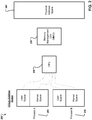
- FIG. 1 depicts an example of a system 100 including a memory device according to implementations of the present disclosure.
- a central processing unit (CPU) 110 may be in communication with main memory in the form of a DRAM 170 and a memory management unit (MMU) 150.
- the system 100 may further include a secondary memory in the form of a remote memory 130, which may be accessed over a network.
- the MMU 150 may operate in the management of memory.
- a page table walker 160 and a translation lookaside buffer (TLB) 165 may be part of, or implemented with, MMU 150.
- the system 100 may additionally include DRAM 170 as physical memory.
- the MMU 150 is a hardware unit that may have memory references passed through it, performing the translation of virtual memory addresses to physical addresses and handling cache control.
- the MMU 150 may use a page table as an in-memory table containing one page table entry (PTE) per page, to map virtual page numbers to physical page numbers in main memory.
- PTE page table entry
- the translation lookaside buffer 165 as an associative cache of PTEs, may be used to avoid the necessity of accessing the main memory every time a virtual address is mapped.
- the MMU 150 may signal a page fault to the CPU 110.
- the CPU 110 may have a cache, which may be a small amount of fast memory built into a processor that may be configured to contain temporary copies of data to reduce processing latency.
- the TLB 165 may be a fixed-size array of recently used pages, which the CPU 110 may check at each memory access.
- the TLB 165 may list virtual address ranges to which physical pages in DRAM 170 are currently assigned. Thus, for example, the TLB 165 may serve as a cache for the MMU 150. In this manner, accesses to virtual addresses listed in the TLB 165 may go directly to the associated physical memory, e.g., DRAM 170.
- accesses to virtual addresses not listed in the TLB 165 i.e., a TLB miss, may trigger a page table lookup, which may be performed by hardware, or by a page fault handler.
- FIG. 2 depicts an example of a system 200 including a memory device according to implementations of the present disclosure.
- the system 200 may include a CPU 220 and a Physical Address Space 240.
- the MMU 230 may interpret virtual addresses to identify corresponding physical addresses. For example, attempts to read, write, or execute memory at virtual addresses may be either translated to corresponding physical addresses, or an interrupt, i.e., a page fault, may be generated to allow software to respond to the attempted access.
- the physical memory addresses may identify a specific memory cell or portion within a piece of the storage hardware making up the physical memory associated with a given read or write operation.
- the virtual memory may provide a software-controlled set of memory addresses, e.g., Virtual Address Space, and may allow each process, e.g., Process A 205 and Process B 210 to have its own virtual memory address range, which may include kernel space and user space.
- the virtual addresses may be interpreted by the MMU 230 using page tables, which may map virtual address ranges to associated stored content. Although the smallest addressable unit to a processor may be a byte or a word, the MMU 230 may manage memory in pages.
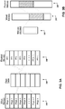
- FIG. 3A depicts an example of a page table 320 for mapping virtual memory 310 to physical memory 330 according to implementations of the present disclosure.
- the page tables 320 may be data structures that contain a list of memory mappings for a process and may be used to track associated resources. For example, each process may have its own set of page tables.
- the virtual address space, e.g., virtual memory 310 may be divided into pages, which may be a contiguous span of addresses of a particular size.
- the pages may be structured such that the starting address of a page is a multiple of the page size.
- the MMU 230 may use the page table 320 to interpret virtual addresses of pages from virtual memory 310 and identify corresponding physical addresses of page frames in physical memory 330.
- page tables may be hierarchical or multi-level, hash-based, or the like, which provides an advantage for huge pages, higher up the hierarchy with a faster page table walk.
- a secondary memory or second tier of memory such as disk-based memory or other second tier memory
- main memory or primary memory such as DRAM.
- a customized kernel driver may manage the second tier of memory with huge pages.
- the kernel driver may reserve physical memory in contiguous regions that are multiples of huge pages for the cache in DRAM.
- the kernel driver may allocate space in huge page multiples, i.e., in multiples of the size of a huge page.
- the kernel driver may implement a page replacement policy, and when data for replacement is selected, a huge page may be paged out to the second tier of memory. That process may occur asynchronously to the running application that requested access to data in memory.
- a page fault handler may transfer only a single small page containing the requested cache line from the second tier of memory to main memory, e.g. DRAM.
- main memory e.g. DRAM.
- the state of each small page that makes up the huge page may be tracked.
- a determination may be made to page-in any remaining small pages and coalesce or reassemble the small pages back into a huge page in DRAM by replacing the existing PTEs with a single PTE for the huge page and flushing any relevant TLB entries from the TLB 165.
- the benefits of huge pages for data that resides in DRAM may be maintained while the cost of page faults may also be reduced by completing the fault handler process after transferring the small page.
- using huge pages may provide the advantage of reducing resource overhead because tracking data at a larger granularity enables a smaller page table having fewer entries.
- Using huge pages may cause the overall write bandwidth to increase if the system always writes out huge pages to the second tier of memory.
- small pages within a huge page that are "hot” e.g., frequently used or recently used, may get paged out to the secondary, slower memory, resulting in additional faults on that "hot" data.
- those issues may be mitigated by the kernel driver dynamically determining when to break up or coalesce huge pages based on huge page and small page statistics. For example, huge pages may be periodically broken up to gather statistics, through PTE access bits, about the small pages within a huge page, as described in more detail below. Further, the driver may maintain both huge pages and small pages, such that when a predetermined number of small pages within a huge page are "hot" or frequently or recently accessed, the small pages may be migrated to a huge page and merged. Conversely, if too many sub-pages, i.e., small pages, within a huge page are "cold", the huge page may be broken up and processed as small pages.
- the entire huge page may not be transferred into main memory, but rather a smaller chunk of data, e.g. a small page, that includes the data for which access is requested may be transferred from secondary memory to main memory.
- the application may access the data requested and continue running. Subsequently, the remainder of the huge page may be transferred into main memory in the background, and the page table entry may be updated accordingly. In this way, the requested data may be accessed more quickly and the system may still reap the benefits of managing huge pages.
- the time required for reading huge pages from secondary memory and writing huge pages to main memory is greater than the time required for reading and writing small pages; and thus, reading only the small page containing the data that is requested to be accessed reduces the time the application or processing thread is suspended or waiting for the data to be transferred from secondary memory to main memory.
- reducing the latency time for transferring data into main memory is more important, as performance critical, than the time for transferring data back to secondary memory because the data transferred out of main memory is typically a page of "cold" data that is transferred in the background with little or no effect on operating performance, whereas the data being transferred into main memory may be delaying the execution of the application or processing thread.
- a page fault may occur when a thread or running program accesses a memory page that is mapped into the virtual address space, but not actually loaded into main memory.
- the MMU 150 or a page fault handler may detect the page fault, and when the page fault is detected, a determination may be made as to whether there is a free page in memory. If there is a free page, page data may be copied from the secondary storage to the free page location in memory. If there is not a free page, a page may be pulled, for example, from a FIFO queue, which may track all the pages in memory in a queue, with the most recent arrival at the back, and the oldest arrival in front.
- the system may write the page to the secondary memory.
- the page table entry associated with the page may be invalidated, and a TLB shootdown for any entries associated with the page may be executed, e.g., causing the TLB entries to be flushed for other processors.
- page data may be copied from the secondary storage to the free page location.
- the page tables may be updated to create a valid PTE by updating the PTE associated with the page to point to the location in the main memory of the page.
- FIG. 3B depicts an example of a portion of memory 305 allocated according to implementations of the present disclosure.
- a page of "cold" data e.g., data that is accessed at a rate that is less than some threshold access rate or that has not been accessed for a particular period of time, may need to be written out to secondary storage, and a page of data may need to be transferred back to main memory when an application tries to access data and a page fault occurs.
- the process of paging in and out of main memory occurs from the processor's perspective as if the system is only working with huge pages.
- a huge page may be transferred out of main memory when cold, i.e., not being used frequently or recently, and when a page needs to be transferred into main memory, a whole huge page of memory may be allocated, even though only a portion of the huge page, e.g., a small page, may be initially transferred.
- memory allocated 305 may correspond to a huge page, and contiguous memory corresponding to the huge page may be allocated in physical memory 325 as well as virtual memory 315.
- a huge page of memory may first be allocated. Then, rather than transferring the whole huge page containing the data requested to be accessed, only the sub-page or small page of data that contains the data requested to be accessed by the application may be transferred into main memory initially. For example, an application may only need to access a byte or a word, such that the whole huge page is not required for the application to continue, and the system may only transfer into main memory a smaller portion of data, e.g., a small page, that includes the data the application needs to continue running. Upon the transferring of that small page, an indication may be made to the application that the requested data has been transferred into main memory or is now available to be accessed from main memory.
- the remaining portion of the huge page may be transferred into main memory in the background.
- breaking up the huge page into small pages is advantageous, for example based on access statistics, and thereby change paging data structures from a single huge page to constituent small pages. If an application subsequently accesses any of the remaining small pages that had not been transferred into main memory, those small pages may be transferred at that time, i.e., when requested to be accessed, with a page fault occurring.
- access statistics may be gathered to identify the "temperature" of pages, e.g., "hot” pages and "cold” pages among the pages within the huge page.
- memory is allocated and reserved in huge page chunks, but a huge page may be broken into small pages to work with smaller page chunks.
- the page table may be updated with a respective PTE for each small page; and when a huge page is reassembled, the page table may be updated by replacing the respective PTEs for each small page with one entry for the full huge page.
- Gathering access statistics for pages may be accomplished through any process or means of determining access of pages, e.g., determining "cold" pages and "hot” pages.
- a process may include periodically breaking up a huge page into small pages, scanning the set of pages and reading an access bit to determine when a small page was last accessed or the frequency or how recently a small page was accessed, and then reassembling the small pages back into the huge page once access statistics have been gathered.
- a sample of accesses to sub-pages or small pages within the huge page may be used to obtain statistical data about access to the small pages.
- page table scanning i.e., a scan through the page table
- page table scanning may be performed via hardware, rather than software requiring CPU overhead, which often results in slower memory access and processing and discarding some otherwise useful cache information.
- the frequency of access of page data e.g., which page data is frequently accessed relative to other pages of data and which page data is infrequently accessed relative to other pages of data may be determined by scanning the page table.
- Each page mapped in the page table e.g., each PTE, may have a flag or access bit that may be set whenever the page is accessed, and then cleared by the CPU after scanning the page table.
- This hardware may be implemented by augmenting the page table walker 160 or MMU 150, which may include one or more page table walkers, e.g., built-in hardware to read the page table and automatically load virtual-to-physical translations into the TLB 165.
- the hardware may be part of the processor architecture, using the page table scanning mechanism in the processor. For example, the hardware may implement a routine to scan through a page table, scanning the PTEs, to determine if an access bit has been set at each PTE since the last scan. The access bit may be cleared after determining that the access bit has been set, and then operations may proceed until the next scan of the page table.
- the scanning may occur periodically, e.g., with a predetermined time period between scans, or the scanning may be triggered by some external event.
- a count may be incremented for each page, respectively.
- a count may be incremented for each page, respectively.
- a profile may be created from the scanning, and the profile may indicate how often and/or how recently each page is accessed.
- the hardware may include one or more counters for each page or bloom filters to maintain the usage statistics, e.g., the count of set access bit or flag, or the results may be stored in memory, e.g., a two-level memory, to allow sorting and filtering, e.g., most and least used pages or more frequently and less frequently accessed pages.
- the hardware may maintain a per-page counter to determine how recently a page was accessed, and each counter may be updated when the respective PTE is scanned.
- the per-page counters may be provided in on-chip SRAM for fast access.
- counting bloom filters may be used to maintain the access statistics about sets of pages, thereby saving area.
- the hardware may use a small amount of private DRAM or may store the counters in system DRAM.
- the pages may be ordered from most used to least used or vice versa.
- a paging process may release or write back one of the least used pages into the secondary memory and may use the location of that least used page to transfer the new page into main memory.
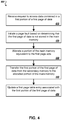
- FIG. 4 depicts a flowchart of an example of a process 400 for memory management, according to implementations of the present disclosure.
- the process 400 may include, at 410, receiving a request to access, from a main memory, data contained in a first portion of a first page of data.
- the first page of data may have a first page size, e.g., a huge page, and the first portion may have a second page size, e.g., a small page, that is less than the first page size.
- a page fault may be initiated based on determining that the first page of data is not stored in the main memory and is stored in a secondary memory.
- a portion of the main memory equivalent to the first page size may be allocated at 430.
- the first portion of the first page of data may be transferred, at 440, from the secondary memory to the allocated portion of the main memory without transferring the entire first page of data.
- a remaining amount of the first page of data may remain stored in the secondary memory.
- a first page table entry associated with the first portion of the first page of data may be updated to point to a location of the allocated portion of the main memory to which the first portion of the first page of data is transferred. Subsequently, the remaining amount of the first page of data may be transferred from the secondary memory to the main memory, for example, in the background while the application continues running.
- respective portions, corresponding to the second page size, of the first page of data may be transferred from the secondary memory to the allocated portion of the main memory until the entire first page of data is stored in the main memory. Further, a respective page table entry for each of the respective portions of the first page of data may be updated to point to respective locations of the respective portions of the first page of data in the main memory. Moreover, once the entire first page of data is stored in the main memory, the first page of data may be coalesced or reassembled from the respective portions of the first page of data transferred from the secondary memory to the allocated portion of the main memory. In accordance with the reassembling, a page table entry associated with the first page of data may be updated to point to a location of the reassembled first page of data in the main memory.
- the system may indicate that the first portion of the first page of data that was requested to be accessed has been transferred to the main memory, so that the application or thread that requested access may continue running by accessing the requested data in main memory.
- An example of a process for memory management may also include determining whether an access bit is set for each page table entry of a page table based on a scan of the page table with a page table scanner.
- the access bit may indicate whether a page associated with the page table entry was accessed in a last scan period.
- at least one of the pages having the first page size e.g., a huge page
- a count for each page may be incremented in response to determining that the access bit is not set for the page table entry associated with the page.
- the access bit may be reset, after determining whether the access bit is set for each page table entry.
- one of a least used pages having the first page size may be determined based on the count for each page and the determined least used page may be released into the secondary memory. Accordingly, a portion of the main memory equivalent to the first page size may be allocated at the location of the released one of the least used pages. Conversely, if the portion of the main memory equivalent to the first page size can be allocated, the first portion of the first page of data may be transferred from the secondary memory to the allocated portion of the main memory.
- one of the least used pages in main memory may be determined based on the count for each page.
- a page fault handler or controller may manage the page transfer and the determined one of the least used pages may be released or written back into the secondary memory. Further, the page of data for which access is requested may be transferred from the secondary memory to the main memory at the location of the released one of the least used pages.
- the page fault handler or controller may manage transferring of the page data from the secondary memory to the main memory.
- execution of the thread or running program may be stalled while the data transfer is managed to service the page fault, as described above. Subsequently, the thread may be released to access the page in the main memory after the page fault is serviced.
- One process to determine which pages are accessed less frequently in the main memory is described above with reference to usage or access statistics for the main memory, e.g., DRAM, based on, for example, a count of the access bit being set.
- the system may determine when to move data from main memory to secondary memory and when to move data from secondary memory to main memory based on the access statistics described above for the main memory.
- pages that are cooling off or being accessed less frequently may be determined by monitoring the PTEs. For example, when the inter-access time for a page satisfies an inter-access time threshold, the system may initiate transfer of the page from main memory to the secondary memory by invalidating the PTE associated with the page, executing a TLB shootdown for any entries associated with the page, and transferring the page from main memory into the secondary memory.
- the DRAM cache and the second tier of memory may be managed by hardware, which may act both as an owner of coherent memory and a user of coherent memory.
- DRAM acts as a cache, managed by the hardware, for paging at a configurable granularity for optimal performance.
- the configurable granularity for optimal performance may depend on application locality and the performance of the second tier of memory.
- the customized kernel driver may map the address space owned by the hardware with huge pages only. In this manner, the system may achieve the benefits of huge pages, such as improved performance due to larger TLB reach, whenever the system accesses this region of memory.
- the hardware may maintain a cache lookup structure to check if a page is present in main memory. When a memory access is received from the host, this lookup structure may be queried. If the page is present, the read or write may be performed directly in main memory. If the page is absent, the data may be fetched from the secondary memory into main memory, e.g., DRAM.
- the cache may perform evictions asynchronously-e.g., "cold" data may be written back to secondary storage in the background to keep a minimum number of pages free to service incoming pages.
- this process may provide a caching mechanism at the page level, such that a cache for paging may be provided with a cache coherent interconnect.
- cache optimizations may be applied. For example, when a page fault occurs and a page is transferred from secondary storage to main memory, the system may determine whether to keep the page in main memory, or if the page is non-temporal, to stream the page and read it once for the given access, or perform pre-fetching by determining to fetch the next page in response to the currently fetched page being accessed. In certain implementations, flags may be set regarding how an application is using memory, and the determination for pre-fetching may be made based on those flags.
- Implementations of the invention and all of the functional operations described in this specification can be implemented in digital electronic circuitry, firmware, or hardware, including the structures disclosed in this specification
- Implementations of the invention can be implemented as one or more computer program products, i.e., one or more modules of computer program instructions encoded on a computer readable medium for execution by, or to control the operation of, data processing apparatus.
- the computer readable medium can be a machine-readable storage device, a machine-readable storage substrate, a memory device, or a combination of one or more of them.
- data processing apparatus encompasses all apparatus, devices, and machines for processing data, including by way of example a programmable processor, a computer, or multiple processors or computers.
- the apparatus can include, in addition to hardware, code that creates an execution environment for the computer program in question, e.g., code that constitutes processor firmware, a protocol stack, a database management system, an operating system, or a combination of one or more of them.
Landscapes
- Engineering & Computer Science (AREA)
- Theoretical Computer Science (AREA)
- Physics & Mathematics (AREA)
- General Engineering & Computer Science (AREA)
- General Physics & Mathematics (AREA)
- Memory System Of A Hierarchy Structure (AREA)
Applications Claiming Priority (2)
| Application Number | Priority Date | Filing Date | Title |
|---|---|---|---|
| US15/273,433 US10108550B2 (en) | 2016-09-22 | 2016-09-22 | Memory management supporting huge pages |
| PCT/US2017/048663 WO2018057235A1 (en) | 2016-09-22 | 2017-08-25 | Memory management supporting huge pages |
Publications (2)
| Publication Number | Publication Date |
|---|---|
| EP3516526A1 EP3516526A1 (en) | 2019-07-31 |
| EP3516526B1 true EP3516526B1 (en) | 2020-10-14 |
Family
ID=59772830
Family Applications (1)
| Application Number | Title | Priority Date | Filing Date |
|---|---|---|---|
| EP17761767.7A Active EP3516526B1 (en) | 2016-09-22 | 2017-08-25 | Memory management supporting huge pages |
Country Status (9)
| Country | Link |
|---|---|
| US (2) | US10108550B2 (enExample) |
| EP (1) | EP3516526B1 (enExample) |
| JP (1) | JP6719027B2 (enExample) |
| KR (1) | KR102273622B1 (enExample) |
| CN (2) | CN109791523B (enExample) |
| DK (1) | DK3516526T3 (enExample) |
| IE (2) | IE20170188A1 (enExample) |
| SG (2) | SG10201707699VA (enExample) |
| WO (1) | WO2018057235A1 (enExample) |
Families Citing this family (28)
| Publication number | Priority date | Publication date | Assignee | Title |
|---|---|---|---|---|
| CN110427340B (zh) * | 2018-04-28 | 2023-08-04 | 伊姆西Ip控股有限责任公司 | 用于文件存储的方法、装置和计算机存储介质 |
| US20190354470A1 (en) * | 2018-05-16 | 2019-11-21 | Sap Se | Reduced Database Backup Memory Usage |
| US10956058B2 (en) * | 2018-08-03 | 2021-03-23 | Western Digital Technologies, Inc. | Tiered storage system with tier configuration by peer storage devices |
| US10949356B2 (en) * | 2019-06-14 | 2021-03-16 | Intel Corporation | Fast page fault handling process implemented on persistent memory |
| US11593186B2 (en) * | 2019-07-17 | 2023-02-28 | Memverge, Inc. | Multi-level caching to deploy local volatile memory, local persistent memory, and remote persistent memory |
| US12086446B2 (en) * | 2019-10-21 | 2024-09-10 | Intel Corporation | Memory and storage pool interfaces |
| JP6972202B2 (ja) * | 2020-02-14 | 2021-11-24 | 株式会社日立製作所 | 計算機システム及びメモリ管理方法 |
| US11829298B2 (en) | 2020-02-28 | 2023-11-28 | Apple Inc. | On-demand memory allocation |
| CN111666230B (zh) * | 2020-05-27 | 2023-08-01 | 江苏华创微系统有限公司 | 在组相联tlb中支持巨页的方法 |
| CN111913893A (zh) * | 2020-06-22 | 2020-11-10 | 成都菁蓉联创科技有限公司 | 保留内存的映射方法和装置、设备和存储介质 |
| US11567880B2 (en) | 2020-08-12 | 2023-01-31 | Microsoft Technology Licensing, Llc | Prevention of RAM access pattern attacks via selective data movement |
| CN114253873A (zh) * | 2020-09-22 | 2022-03-29 | 华为技术有限公司 | 内存管理方法、装置、设备和存储介质 |
| CN112148736B (zh) * | 2020-09-23 | 2024-03-12 | 抖音视界有限公司 | 缓存数据的方法、设备及存储介质 |
| US20220382478A1 (en) * | 2021-06-01 | 2022-12-01 | Samsung Electronics Co., Ltd. | Systems, methods, and apparatus for page migration in memory systems |
| CN113608866B (zh) * | 2021-07-13 | 2024-10-25 | 阿里巴巴创新公司 | 内存分配方法及装置 |
| CN115904642A (zh) * | 2021-08-19 | 2023-04-04 | 北京字节跳动网络技术有限公司 | 云服务器控制方法、装置、存储介质及电子设备 |
| US20220012209A1 (en) * | 2021-09-20 | 2022-01-13 | Intel Corporation | Apparatus, system and method to sample page table entry metadata between page walks |
| CN113641464A (zh) * | 2021-10-15 | 2021-11-12 | 云宏信息科技股份有限公司 | Xen平台的内存配置方法、系统及计算机可读存储介质 |
| US12579073B2 (en) | 2022-05-23 | 2026-03-17 | Intel Corporation | Apparatus and method for intelligent memory page management |
| US20230004302A1 (en) * | 2022-09-14 | 2023-01-05 | Intel Corporation | Apparatus, Device, Method, and Computer Program for Managing Memory of a Computer System |
| US12147352B2 (en) * | 2022-10-20 | 2024-11-19 | International Business Machines Corporation | Dynamic tuning of larger pages during runtime |
| CN115794397A (zh) * | 2022-11-29 | 2023-03-14 | 阿里云计算有限公司 | 冷热页管理加速设备、方法、mmu、处理器及电子设备 |
| CN118377606A (zh) * | 2023-01-20 | 2024-07-23 | 华为技术有限公司 | 内存访问的页错误处理方法及装置 |
| US20240256459A1 (en) * | 2023-01-26 | 2024-08-01 | Vmware, Inc. | System and method for managing a memory hierarchy |
| CN116185903A (zh) * | 2023-02-28 | 2023-05-30 | 阿里云计算有限公司 | 页面整合方法、装置、电子设备及存储介质 |
| US12481588B2 (en) | 2023-03-12 | 2025-11-25 | Samsung Electronics Co., Ltd. | Systems and methods for memory representation and management |
| US12423229B2 (en) | 2023-03-16 | 2025-09-23 | Samsung Electronics Co., Ltd. | Systems and methods for memory representation and tracking |
| CN118732931A (zh) * | 2023-03-31 | 2024-10-01 | 华为技术有限公司 | 内存数据迁移方法和相关设备 |
Family Cites Families (24)
| Publication number | Priority date | Publication date | Assignee | Title |
|---|---|---|---|---|
| US5361345A (en) | 1991-09-19 | 1994-11-01 | Hewlett-Packard Company | Critical line first paging system |
| US5987561A (en) * | 1995-08-31 | 1999-11-16 | Advanced Micro Devices, Inc. | Superscalar microprocessor employing a data cache capable of performing store accesses in a single clock cycle |
| US5960463A (en) * | 1996-05-16 | 1999-09-28 | Advanced Micro Devices, Inc. | Cache controller with table walk logic tightly coupled to second level access logic |
| US6112285A (en) | 1997-09-23 | 2000-08-29 | Silicon Graphics, Inc. | Method, system and computer program product for virtual memory support for managing translation look aside buffers with multiple page size support |
| US6804729B2 (en) | 2002-09-30 | 2004-10-12 | International Business Machines Corporation | Migrating a memory page by modifying a page migration state of a state machine associated with a DMA mapper based on a state notification from an operating system kernel |
| US7447869B2 (en) * | 2005-04-07 | 2008-11-04 | Ati Technologies, Inc. | Method and apparatus for fragment processing in a virtual memory system |
| US7519781B1 (en) | 2005-12-19 | 2009-04-14 | Nvidia Corporation | Physically-based page characterization data |
| US8543792B1 (en) | 2006-09-19 | 2013-09-24 | Nvidia Corporation | Memory access techniques including coalesing page table entries |
| US7917725B2 (en) | 2007-09-11 | 2011-03-29 | QNX Software Systems GmbH & Co., KG | Processing system implementing variable page size memory organization using a multiple page per entry translation lookaside buffer |
| JP2009069969A (ja) * | 2007-09-11 | 2009-04-02 | Canon Inc | 情報処理方法および情報処理装置、プログラム |
| US9244855B2 (en) * | 2007-12-31 | 2016-01-26 | Intel Corporation | Method, system, and apparatus for page sizing extension |
| US9208084B2 (en) * | 2009-06-29 | 2015-12-08 | Oracle America, Inc. | Extended main memory hierarchy having flash memory for page fault handling |
| US8195917B2 (en) | 2009-07-01 | 2012-06-05 | Advanced Micro Devices, Inc. | Extended page size using aggregated small pages |
| US8615642B2 (en) | 2009-10-14 | 2013-12-24 | International Business Machines Corporation | Automatic page promotion and demotion in multiple page size environments |
| US8533382B2 (en) * | 2010-01-06 | 2013-09-10 | Vmware, Inc. | Method and system for frequent checkpointing |
| US9158701B2 (en) | 2012-07-03 | 2015-10-13 | International Business Machines Corporation | Process-specific views of large frame pages with variable granularity |
| US10133677B2 (en) | 2013-03-14 | 2018-11-20 | Nvidia Corporation | Opportunistic migration of memory pages in a unified virtual memory system |
| US20150058520A1 (en) | 2013-08-22 | 2015-02-26 | International Business Machines Corporation | Detection of hot pages for partition migration |
| US9864698B2 (en) | 2013-11-04 | 2018-01-09 | International Business Machines Corporation | Resolving cache lookup of large pages with variable granularity |
| US9535831B2 (en) | 2014-01-10 | 2017-01-03 | Advanced Micro Devices, Inc. | Page migration in a 3D stacked hybrid memory |
| US9501422B2 (en) | 2014-06-11 | 2016-11-22 | Vmware, Inc. | Identification of low-activity large memory pages |
| CN105095099B (zh) | 2015-07-21 | 2017-12-29 | 浙江大学 | 一种基于内存页位图变更的大内存页整合方法 |
| US10037173B2 (en) | 2016-08-12 | 2018-07-31 | Google Llc | Hybrid memory management |
| US10152427B2 (en) | 2016-08-12 | 2018-12-11 | Google Llc | Hybrid memory management |
-
2016
- 2016-09-22 US US15/273,433 patent/US10108550B2/en active Active
-
2017
- 2017-08-25 WO PCT/US2017/048663 patent/WO2018057235A1/en not_active Ceased
- 2017-08-25 JP JP2019536814A patent/JP6719027B2/ja active Active
- 2017-08-25 EP EP17761767.7A patent/EP3516526B1/en active Active
- 2017-08-25 CN CN201780058759.7A patent/CN109791523B/zh active Active
- 2017-08-25 CN CN202310717151.8A patent/CN116701250A/zh active Pending
- 2017-08-25 DK DK17761767.7T patent/DK3516526T3/da active
- 2017-08-25 KR KR1020197011367A patent/KR102273622B1/ko active Active
- 2017-09-18 SG SG10201707699VA patent/SG10201707699VA/en unknown
- 2017-09-18 SG SG10201903332RA patent/SG10201903332RA/en unknown
- 2017-09-20 IE IE20170188A patent/IE20170188A1/en not_active IP Right Cessation
- 2017-09-20 IE IE20180302A patent/IE87058B1/en unknown
-
2018
- 2018-08-27 US US16/113,285 patent/US10474580B2/en active Active
Non-Patent Citations (1)
| Title |
|---|
| None * |
Also Published As
| Publication number | Publication date |
|---|---|
| KR102273622B1 (ko) | 2021-07-06 |
| US10474580B2 (en) | 2019-11-12 |
| WO2018057235A1 (en) | 2018-03-29 |
| IE87058B1 (en) | 2019-10-16 |
| IE20170188A1 (en) | 2018-04-04 |
| IE20180302A1 (en) | 2018-10-31 |
| KR20190052106A (ko) | 2019-05-15 |
| DK3516526T3 (da) | 2020-11-30 |
| US20180081816A1 (en) | 2018-03-22 |
| JP6719027B2 (ja) | 2020-07-08 |
| JP2019532450A (ja) | 2019-11-07 |
| US20180365157A1 (en) | 2018-12-20 |
| CN109791523B (zh) | 2023-07-14 |
| CN116701250A (zh) | 2023-09-05 |
| SG10201903332RA (en) | 2019-05-30 |
| SG10201707699VA (en) | 2018-04-27 |
| CN109791523A (zh) | 2019-05-21 |
| EP3516526A1 (en) | 2019-07-31 |
| US10108550B2 (en) | 2018-10-23 |
Similar Documents
| Publication | Publication Date | Title |
|---|---|---|
| EP3516526B1 (en) | Memory management supporting huge pages | |
| US10705975B2 (en) | Hybrid memory management | |
| CN111177030B (zh) | 混合存储器管理 | |
| KR102665339B1 (ko) | 변환 색인 버퍼 축출 기반 캐시 교체 | |
| US10310985B2 (en) | Systems and methods for accessing and managing a computing system memory | |
| US20110161597A1 (en) | Combined Memory Including a Logical Partition in a Storage Memory Accessed Through an IO Controller | |
| CN110059027A (zh) | 执行维护操作的装置和方法 | |
| CN109983538B (zh) | 存储地址转换 | |
| CN110046107A (zh) | 存储器地址转换 | |
| CN108108312A (zh) | 一种高速缓存清理方法及处理器 | |
| JP7311959B2 (ja) | 複数のデータ・タイプのためのデータ・ストレージ | |
| HK40100521A (zh) | 支持巨页的内存管理 | |
| HK1246906A1 (en) | Hybrid memory management | |
| HK1246906A (en) | Hybrid memory management | |
| Bletsch | ECE 650 Systems Programming & Engineering Spring 2018 | |
| CN118349487A (zh) | 支持多实例图形处理单元之计算系统及芯片 |
Legal Events
| Date | Code | Title | Description |
|---|---|---|---|
| STAA | Information on the status of an ep patent application or granted ep patent |
Free format text: STATUS: UNKNOWN |
|
| STAA | Information on the status of an ep patent application or granted ep patent |
Free format text: STATUS: THE INTERNATIONAL PUBLICATION HAS BEEN MADE |
|
| PUAI | Public reference made under article 153(3) epc to a published international application that has entered the european phase |
Free format text: ORIGINAL CODE: 0009012 |
|
| STAA | Information on the status of an ep patent application or granted ep patent |
Free format text: STATUS: REQUEST FOR EXAMINATION WAS MADE |
|
| 17P | Request for examination filed |
Effective date: 20190327 |
|
| AK | Designated contracting states |
Kind code of ref document: A1 Designated state(s): AL AT BE BG CH CY CZ DE DK EE ES FI FR GB GR HR HU IE IS IT LI LT LU LV MC MK MT NL NO PL PT RO RS SE SI SK SM TR |
|
| AX | Request for extension of the european patent |
Extension state: BA ME |
|
| STAA | Information on the status of an ep patent application or granted ep patent |
Free format text: STATUS: EXAMINATION IS IN PROGRESS |
|
| DAV | Request for validation of the european patent (deleted) | ||
| DAX | Request for extension of the european patent (deleted) | ||
| 17Q | First examination report despatched |
Effective date: 20200103 |
|
| REG | Reference to a national code |
Ref country code: DE Ref legal event code: R079 Ref document number: 602017025540 Country of ref document: DE Free format text: PREVIOUS MAIN CLASS: G06F0012100900 Ipc: G06F0012020000 |
|
| GRAP | Despatch of communication of intention to grant a patent |
Free format text: ORIGINAL CODE: EPIDOSNIGR1 |
|
| STAA | Information on the status of an ep patent application or granted ep patent |
Free format text: STATUS: GRANT OF PATENT IS INTENDED |
|
| RIC1 | Information provided on ipc code assigned before grant |
Ipc: G06F 12/1009 20160101ALI20200529BHEP Ipc: G06F 12/1027 20160101ALI20200529BHEP Ipc: G06F 12/0815 20160101ALI20200529BHEP Ipc: G06F 12/04 20060101ALI20200529BHEP Ipc: G06F 12/12 20160101ALI20200529BHEP Ipc: G06F 12/02 20060101AFI20200529BHEP Ipc: G06F 12/0873 20160101ALI20200529BHEP |
|
| INTG | Intention to grant announced |
Effective date: 20200629 |
|
| GRAS | Grant fee paid |
Free format text: ORIGINAL CODE: EPIDOSNIGR3 |
|
| GRAA | (expected) grant |
Free format text: ORIGINAL CODE: 0009210 |
|
| STAA | Information on the status of an ep patent application or granted ep patent |
Free format text: STATUS: THE PATENT HAS BEEN GRANTED |
|
| AK | Designated contracting states |
Kind code of ref document: B1 Designated state(s): AL AT BE BG CH CY CZ DE DK EE ES FI FR GB GR HR HU IE IS IT LI LT LU LV MC MK MT NL NO PL PT RO RS SE SI SK SM TR |
|
| REG | Reference to a national code |
Ref country code: GB Ref legal event code: FG4D |
|
| REG | Reference to a national code |
Ref country code: AT Ref legal event code: REF Ref document number: 1324255 Country of ref document: AT Kind code of ref document: T Effective date: 20201015 Ref country code: CH Ref legal event code: EP |
|
| REG | Reference to a national code |
Ref country code: DE Ref legal event code: R096 Ref document number: 602017025540 Country of ref document: DE |
|
| REG | Reference to a national code |
Ref country code: IE Ref legal event code: FG4D |
|
| REG | Reference to a national code |
Ref country code: DK Ref legal event code: T3 Effective date: 20201123 Ref country code: CH Ref legal event code: NV Representative=s name: RENTSCH PARTNER AG, CH |
|
| REG | Reference to a national code |
Ref country code: SE Ref legal event code: TRGR |
|
| REG | Reference to a national code |
Ref country code: NL Ref legal event code: FP |
|
| REG | Reference to a national code |
Ref country code: FI Ref legal event code: FGE |
|
| REG | Reference to a national code |
Ref country code: AT Ref legal event code: MK05 Ref document number: 1324255 Country of ref document: AT Kind code of ref document: T Effective date: 20201014 |
|
| PG25 | Lapsed in a contracting state [announced via postgrant information from national office to epo] |
Ref country code: GR Free format text: LAPSE BECAUSE OF FAILURE TO SUBMIT A TRANSLATION OF THE DESCRIPTION OR TO PAY THE FEE WITHIN THE PRESCRIBED TIME-LIMIT Effective date: 20210115 Ref country code: NO Free format text: LAPSE BECAUSE OF FAILURE TO SUBMIT A TRANSLATION OF THE DESCRIPTION OR TO PAY THE FEE WITHIN THE PRESCRIBED TIME-LIMIT Effective date: 20210114 Ref country code: RS Free format text: LAPSE BECAUSE OF FAILURE TO SUBMIT A TRANSLATION OF THE DESCRIPTION OR TO PAY THE FEE WITHIN THE PRESCRIBED TIME-LIMIT Effective date: 20201014 Ref country code: PT Free format text: LAPSE BECAUSE OF FAILURE TO SUBMIT A TRANSLATION OF THE DESCRIPTION OR TO PAY THE FEE WITHIN THE PRESCRIBED TIME-LIMIT Effective date: 20210215 |
|
| REG | Reference to a national code |
Ref country code: LT Ref legal event code: MG4D |
|
| PG25 | Lapsed in a contracting state [announced via postgrant information from national office to epo] |
Ref country code: BG Free format text: LAPSE BECAUSE OF FAILURE TO SUBMIT A TRANSLATION OF THE DESCRIPTION OR TO PAY THE FEE WITHIN THE PRESCRIBED TIME-LIMIT Effective date: 20210114 Ref country code: LV Free format text: LAPSE BECAUSE OF FAILURE TO SUBMIT A TRANSLATION OF THE DESCRIPTION OR TO PAY THE FEE WITHIN THE PRESCRIBED TIME-LIMIT Effective date: 20201014 Ref country code: PL Free format text: LAPSE BECAUSE OF FAILURE TO SUBMIT A TRANSLATION OF THE DESCRIPTION OR TO PAY THE FEE WITHIN THE PRESCRIBED TIME-LIMIT Effective date: 20201014 Ref country code: IS Free format text: LAPSE BECAUSE OF FAILURE TO SUBMIT A TRANSLATION OF THE DESCRIPTION OR TO PAY THE FEE WITHIN THE PRESCRIBED TIME-LIMIT Effective date: 20210214 Ref country code: AT Free format text: LAPSE BECAUSE OF FAILURE TO SUBMIT A TRANSLATION OF THE DESCRIPTION OR TO PAY THE FEE WITHIN THE PRESCRIBED TIME-LIMIT Effective date: 20201014 Ref country code: ES Free format text: LAPSE BECAUSE OF FAILURE TO SUBMIT A TRANSLATION OF THE DESCRIPTION OR TO PAY THE FEE WITHIN THE PRESCRIBED TIME-LIMIT Effective date: 20201014 |
|
| PG25 | Lapsed in a contracting state [announced via postgrant information from national office to epo] |
Ref country code: HR Free format text: LAPSE BECAUSE OF FAILURE TO SUBMIT A TRANSLATION OF THE DESCRIPTION OR TO PAY THE FEE WITHIN THE PRESCRIBED TIME-LIMIT Effective date: 20201014 |
|
| REG | Reference to a national code |
Ref country code: DE Ref legal event code: R097 Ref document number: 602017025540 Country of ref document: DE |
|
| PG25 | Lapsed in a contracting state [announced via postgrant information from national office to epo] |
Ref country code: SM Free format text: LAPSE BECAUSE OF FAILURE TO SUBMIT A TRANSLATION OF THE DESCRIPTION OR TO PAY THE FEE WITHIN THE PRESCRIBED TIME-LIMIT Effective date: 20201014 Ref country code: LT Free format text: LAPSE BECAUSE OF FAILURE TO SUBMIT A TRANSLATION OF THE DESCRIPTION OR TO PAY THE FEE WITHIN THE PRESCRIBED TIME-LIMIT Effective date: 20201014 Ref country code: CZ Free format text: LAPSE BECAUSE OF FAILURE TO SUBMIT A TRANSLATION OF THE DESCRIPTION OR TO PAY THE FEE WITHIN THE PRESCRIBED TIME-LIMIT Effective date: 20201014 Ref country code: EE Free format text: LAPSE BECAUSE OF FAILURE TO SUBMIT A TRANSLATION OF THE DESCRIPTION OR TO PAY THE FEE WITHIN THE PRESCRIBED TIME-LIMIT Effective date: 20201014 Ref country code: SK Free format text: LAPSE BECAUSE OF FAILURE TO SUBMIT A TRANSLATION OF THE DESCRIPTION OR TO PAY THE FEE WITHIN THE PRESCRIBED TIME-LIMIT Effective date: 20201014 Ref country code: RO Free format text: LAPSE BECAUSE OF FAILURE TO SUBMIT A TRANSLATION OF THE DESCRIPTION OR TO PAY THE FEE WITHIN THE PRESCRIBED TIME-LIMIT Effective date: 20201014 |
|
| PLBE | No opposition filed within time limit |
Free format text: ORIGINAL CODE: 0009261 |
|
| STAA | Information on the status of an ep patent application or granted ep patent |
Free format text: STATUS: NO OPPOSITION FILED WITHIN TIME LIMIT |
|
| 26N | No opposition filed |
Effective date: 20210715 |
|
| PG25 | Lapsed in a contracting state [announced via postgrant information from national office to epo] |
Ref country code: AL Free format text: LAPSE BECAUSE OF FAILURE TO SUBMIT A TRANSLATION OF THE DESCRIPTION OR TO PAY THE FEE WITHIN THE PRESCRIBED TIME-LIMIT Effective date: 20201014 Ref country code: IT Free format text: LAPSE BECAUSE OF FAILURE TO SUBMIT A TRANSLATION OF THE DESCRIPTION OR TO PAY THE FEE WITHIN THE PRESCRIBED TIME-LIMIT Effective date: 20201014 |
|
| PG25 | Lapsed in a contracting state [announced via postgrant information from national office to epo] |
Ref country code: SI Free format text: LAPSE BECAUSE OF FAILURE TO SUBMIT A TRANSLATION OF THE DESCRIPTION OR TO PAY THE FEE WITHIN THE PRESCRIBED TIME-LIMIT Effective date: 20201014 |
|
| PG25 | Lapsed in a contracting state [announced via postgrant information from national office to epo] |
Ref country code: MC Free format text: LAPSE BECAUSE OF FAILURE TO SUBMIT A TRANSLATION OF THE DESCRIPTION OR TO PAY THE FEE WITHIN THE PRESCRIBED TIME-LIMIT Effective date: 20201014 |
|
| PG25 | Lapsed in a contracting state [announced via postgrant information from national office to epo] |
Ref country code: IS Free format text: LAPSE BECAUSE OF FAILURE TO SUBMIT A TRANSLATION OF THE DESCRIPTION OR TO PAY THE FEE WITHIN THE PRESCRIBED TIME-LIMIT Effective date: 20210214 Ref country code: LU Free format text: LAPSE BECAUSE OF NON-PAYMENT OF DUE FEES Effective date: 20210825 |
|
| PG25 | Lapsed in a contracting state [announced via postgrant information from national office to epo] |
Ref country code: IE Free format text: LAPSE BECAUSE OF NON-PAYMENT OF DUE FEES Effective date: 20210825 |
|
| P01 | Opt-out of the competence of the unified patent court (upc) registered |
Effective date: 20230509 |
|
| PG25 | Lapsed in a contracting state [announced via postgrant information from national office to epo] |
Ref country code: CY Free format text: LAPSE BECAUSE OF FAILURE TO SUBMIT A TRANSLATION OF THE DESCRIPTION OR TO PAY THE FEE WITHIN THE PRESCRIBED TIME-LIMIT Effective date: 20201014 |
|
| PG25 | Lapsed in a contracting state [announced via postgrant information from national office to epo] |
Ref country code: HU Free format text: LAPSE BECAUSE OF FAILURE TO SUBMIT A TRANSLATION OF THE DESCRIPTION OR TO PAY THE FEE WITHIN THE PRESCRIBED TIME-LIMIT; INVALID AB INITIO Effective date: 20170825 |
|
| PG25 | Lapsed in a contracting state [announced via postgrant information from national office to epo] |
Ref country code: MK Free format text: LAPSE BECAUSE OF FAILURE TO SUBMIT A TRANSLATION OF THE DESCRIPTION OR TO PAY THE FEE WITHIN THE PRESCRIBED TIME-LIMIT Effective date: 20201014 |
|
| PG25 | Lapsed in a contracting state [announced via postgrant information from national office to epo] |
Ref country code: MT Free format text: LAPSE BECAUSE OF FAILURE TO SUBMIT A TRANSLATION OF THE DESCRIPTION OR TO PAY THE FEE WITHIN THE PRESCRIBED TIME-LIMIT Effective date: 20201014 |
|
| PGFP | Annual fee paid to national office [announced via postgrant information from national office to epo] |
Ref country code: NL Payment date: 20250826 Year of fee payment: 9 |
|
| PGFP | Annual fee paid to national office [announced via postgrant information from national office to epo] |
Ref country code: FI Payment date: 20250825 Year of fee payment: 9 |
|
| PGFP | Annual fee paid to national office [announced via postgrant information from national office to epo] |
Ref country code: DK Payment date: 20250825 Year of fee payment: 9 Ref country code: DE Payment date: 20250827 Year of fee payment: 9 |
|
| PGFP | Annual fee paid to national office [announced via postgrant information from national office to epo] |
Ref country code: BE Payment date: 20250827 Year of fee payment: 9 Ref country code: GB Payment date: 20250827 Year of fee payment: 9 |
|
| PGFP | Annual fee paid to national office [announced via postgrant information from national office to epo] |
Ref country code: FR Payment date: 20250825 Year of fee payment: 9 |
|
| PGFP | Annual fee paid to national office [announced via postgrant information from national office to epo] |
Ref country code: SE Payment date: 20250827 Year of fee payment: 9 Ref country code: CH Payment date: 20250901 Year of fee payment: 9 |
|
| PG25 | Lapsed in a contracting state [announced via postgrant information from national office to epo] |
Ref country code: TR Free format text: LAPSE BECAUSE OF FAILURE TO SUBMIT A TRANSLATION OF THE DESCRIPTION OR TO PAY THE FEE WITHIN THE PRESCRIBED TIME-LIMIT Effective date: 20201014 |