EP3514941B1 - Appareil de conversion de puissance et système électrique - Google Patents
Appareil de conversion de puissance et système électrique Download PDFInfo
- Publication number
- EP3514941B1 EP3514941B1 EP17850494.0A EP17850494A EP3514941B1 EP 3514941 B1 EP3514941 B1 EP 3514941B1 EP 17850494 A EP17850494 A EP 17850494A EP 3514941 B1 EP3514941 B1 EP 3514941B1
- Authority
- EP
- European Patent Office
- Prior art keywords
- arm
- voltage
- power conversion
- converter
- command value
- Prior art date
- Legal status (The legal status is an assumption and is not a legal conclusion. Google has not performed a legal analysis and makes no representation as to the accuracy of the status listed.)
- Active
Links
- 238000006243 chemical reaction Methods 0.000 title claims description 135
- 239000003990 capacitor Substances 0.000 claims description 45
- 238000001514 detection method Methods 0.000 claims description 17
- 239000004065 semiconductor Substances 0.000 claims description 14
- 230000008030 elimination Effects 0.000 claims description 8
- 238000003379 elimination reaction Methods 0.000 claims description 8
- 238000010586 diagram Methods 0.000 description 19
- 230000005540 biological transmission Effects 0.000 description 8
- 238000000034 method Methods 0.000 description 8
- 238000012806 monitoring device Methods 0.000 description 8
- 230000000694 effects Effects 0.000 description 7
- 230000000977 initiatory effect Effects 0.000 description 4
- 230000001629 suppression Effects 0.000 description 3
- 230000002457 bidirectional effect Effects 0.000 description 2
- 238000010606 normalization Methods 0.000 description 2
- 238000004804 winding Methods 0.000 description 2
- 230000003247 decreasing effect Effects 0.000 description 1
- 230000001419 dependent effect Effects 0.000 description 1
- 230000006866 deterioration Effects 0.000 description 1
- 238000009499 grossing Methods 0.000 description 1
- 238000012544 monitoring process Methods 0.000 description 1
Images


Classifications
-
- H—ELECTRICITY
- H02—GENERATION; CONVERSION OR DISTRIBUTION OF ELECTRIC POWER
- H02M—APPARATUS FOR CONVERSION BETWEEN AC AND AC, BETWEEN AC AND DC, OR BETWEEN DC AND DC, AND FOR USE WITH MAINS OR SIMILAR POWER SUPPLY SYSTEMS; CONVERSION OF DC OR AC INPUT POWER INTO SURGE OUTPUT POWER; CONTROL OR REGULATION THEREOF
- H02M7/00—Conversion of ac power input into dc power output; Conversion of dc power input into ac power output
- H02M7/42—Conversion of dc power input into ac power output without possibility of reversal
- H02M7/44—Conversion of dc power input into ac power output without possibility of reversal by static converters
- H02M7/48—Conversion of dc power input into ac power output without possibility of reversal by static converters using discharge tubes with control electrode or semiconductor devices with control electrode
- H02M7/483—Converters with outputs that each can have more than two voltages levels
- H02M7/4835—Converters with outputs that each can have more than two voltages levels comprising two or more cells, each including a switchable capacitor, the capacitors having a nominal charge voltage which corresponds to a given fraction of the input voltage, and the capacitors being selectively connected in series to determine the instantaneous output voltage
-
- G—PHYSICS
- G01—MEASURING; TESTING
- G01R—MEASURING ELECTRIC VARIABLES; MEASURING MAGNETIC VARIABLES
- G01R19/00—Arrangements for measuring currents or voltages or for indicating presence or sign thereof
- G01R19/165—Indicating that current or voltage is either above or below a predetermined value or within or outside a predetermined range of values
-
- H—ELECTRICITY
- H02—GENERATION; CONVERSION OR DISTRIBUTION OF ELECTRIC POWER
- H02M—APPARATUS FOR CONVERSION BETWEEN AC AND AC, BETWEEN AC AND DC, OR BETWEEN DC AND DC, AND FOR USE WITH MAINS OR SIMILAR POWER SUPPLY SYSTEMS; CONVERSION OF DC OR AC INPUT POWER INTO SURGE OUTPUT POWER; CONTROL OR REGULATION THEREOF
- H02M1/00—Details of apparatus for conversion
- H02M1/32—Means for protecting converters other than automatic disconnection
-
- H—ELECTRICITY
- H02—GENERATION; CONVERSION OR DISTRIBUTION OF ELECTRIC POWER
- H02M—APPARATUS FOR CONVERSION BETWEEN AC AND AC, BETWEEN AC AND DC, OR BETWEEN DC AND DC, AND FOR USE WITH MAINS OR SIMILAR POWER SUPPLY SYSTEMS; CONVERSION OF DC OR AC INPUT POWER INTO SURGE OUTPUT POWER; CONTROL OR REGULATION THEREOF
- H02M7/00—Conversion of ac power input into dc power output; Conversion of dc power input into ac power output
- H02M7/42—Conversion of dc power input into ac power output without possibility of reversal
- H02M7/44—Conversion of dc power input into ac power output without possibility of reversal by static converters
- H02M7/48—Conversion of dc power input into ac power output without possibility of reversal by static converters using discharge tubes with control electrode or semiconductor devices with control electrode
- H02M7/483—Converters with outputs that each can have more than two voltages levels
- H02M7/49—Combination of the output voltage waveforms of a plurality of converters
-
- H—ELECTRICITY
- H02—GENERATION; CONVERSION OR DISTRIBUTION OF ELECTRIC POWER
- H02M—APPARATUS FOR CONVERSION BETWEEN AC AND AC, BETWEEN AC AND DC, OR BETWEEN DC AND DC, AND FOR USE WITH MAINS OR SIMILAR POWER SUPPLY SYSTEMS; CONVERSION OF DC OR AC INPUT POWER INTO SURGE OUTPUT POWER; CONTROL OR REGULATION THEREOF
- H02M7/00—Conversion of ac power input into dc power output; Conversion of dc power input into ac power output
- H02M7/66—Conversion of ac power input into dc power output; Conversion of dc power input into ac power output with possibility of reversal
- H02M7/68—Conversion of ac power input into dc power output; Conversion of dc power input into ac power output with possibility of reversal by static converters
- H02M7/72—Conversion of ac power input into dc power output; Conversion of dc power input into ac power output with possibility of reversal by static converters using discharge tubes with control electrode or semiconductor devices with control electrode
- H02M7/79—Conversion of ac power input into dc power output; Conversion of dc power input into ac power output with possibility of reversal by static converters using discharge tubes with control electrode or semiconductor devices with control electrode using devices of a triode or transistor type requiring continuous application of a control signal
- H02M7/797—Conversion of ac power input into dc power output; Conversion of dc power input into ac power output with possibility of reversal by static converters using discharge tubes with control electrode or semiconductor devices with control electrode using devices of a triode or transistor type requiring continuous application of a control signal using semiconductor devices only
-
- H—ELECTRICITY
- H02—GENERATION; CONVERSION OR DISTRIBUTION OF ELECTRIC POWER
- H02M—APPARATUS FOR CONVERSION BETWEEN AC AND AC, BETWEEN AC AND DC, OR BETWEEN DC AND DC, AND FOR USE WITH MAINS OR SIMILAR POWER SUPPLY SYSTEMS; CONVERSION OF DC OR AC INPUT POWER INTO SURGE OUTPUT POWER; CONTROL OR REGULATION THEREOF
- H02M1/00—Details of apparatus for conversion
- H02M1/0003—Details of control, feedback or regulation circuits
- H02M1/0006—Arrangements for supplying an adequate voltage to the control circuit of converters
-
- H—ELECTRICITY
- H02—GENERATION; CONVERSION OR DISTRIBUTION OF ELECTRIC POWER
- H02M—APPARATUS FOR CONVERSION BETWEEN AC AND AC, BETWEEN AC AND DC, OR BETWEEN DC AND DC, AND FOR USE WITH MAINS OR SIMILAR POWER SUPPLY SYSTEMS; CONVERSION OF DC OR AC INPUT POWER INTO SURGE OUTPUT POWER; CONTROL OR REGULATION THEREOF
- H02M1/00—Details of apparatus for conversion
- H02M1/0083—Converters characterised by their input or output configuration
- H02M1/0085—Partially controlled bridges
Definitions
- the present invention relates to a large-capacity power conversion device in which an arm is formed by converter cells each including a plurality of semiconductor switching elements and a DC capacitor and which performs power conversion between an AC circuit and a DC circuit, and a power system including the power conversion device, and in particular, relates to restart control after short-circuit current of high-voltage DC lines is suppressed and the short-circuit is eliminated.
- output of a power converter is high voltage and large current, and therefore many of the large-capacity power conversion devices are configured such that a plurality of converters are multiplexed in series or in parallel.
- the multiplexing of the converters is not only for the purpose of increasing the capacity of the power converter.
- the transformer multiplexing has an advantage that DC currents of the converters can be made to be the same current because the AC side is insulated by the transformer.
- the output voltage is high voltage, the configuration of the multiplexed transformer is complicated, and the cost of the transformer increases.
- a multilevel converter is proposed in which outputs of a plurality of converters are connected in cascade, and one of such multilevel converters is a modular multilevel converter (hereinafter, referred to as MMC).
- the MMC is formed by an arm in which a plurality of unit converters (hereinafter, referred to as converter cells) which are called cells are connected in cascade.
- Each converter cell includes a plurality of semiconductor switching elements and a DC capacitor. Then, through ON/OFF switching of the semiconductor switching elements, both-end voltage of the DC capacitor and zero voltage are output.
- each phase arm is formed individually for each phase. These phase arms are connected in parallel to each other, and connection terminals at both ends connected in parallel are used as DC terminals.
- Each phase arm is composed of a positive arm and a negative arm each having a half of the total converter cells connected in cascade. The connection point between the positive arm and the negative arm serves as an AC-side input/output terminal.
- each converter cell Since outputs of each converter cell in the MMC are connected to both of the AC end and the DC end of the MMC, each converter cell has a characteristic of outputting both of DC current and AC current. That is, current flowing through each arm contains an AC component and a DC component. Therefore, in the MMC, the plurality of current components are controlled.
- the MMC since the MMC is connected to both of the AC end and the DC end, it is necessary to cope with short-circuit, grid disturbance, and the like that can occur at each terminal.
- short-circuit or the like occurs at the DC end, power transmission is stopped until the short-circuit is eliminated. Therefore, it is necessary to swiftly eliminate the short-circuit and restart rated power transmission. If short-circuit occurs, the voltage of the DC end becomes zero, and therefore it is necessary to raise the DC output voltage of the power conversion device to the rated value in order to start power transmission after the short-circuit has been eliminated.
- a power conversion device restart method in which DC voltage is gradually raised in a state of being interconnected with the AC grid, whereby overvoltage of DC lines is suppressed and the DC voltage is stably restored as follows.
- Each arm of a power converter is formed by two types of unit converters, i.e., full-bridge-type unit converter and bidirectional-chopper-type unit converter.
- a command value distributing unit distributes an AC voltage command value and a DC voltage command value to an output voltage command value for a bidirectional chopper group and an output voltage command value for a full-bridge group.
- a gate pulse generation unit generates gate signals to be given to the respective full-bridge-type unit converters and gate signals to be given to the respective bidirectional-chopper-type unit converters so that the voltage command values and the actual voltages coincide with each other as much as possible.
- a DC failure detection unit changes a DC failure detection signal from 0 to 1 after a certain time period has elapsed since detection of DC failure. At this time, the DC failure detection unit changes the DC failure detection signal from 0 to 1 in a ramp function shape with a certain slope.
- the DC failure detection signal is given to the above command distributing unit.
- the command value distributing unit returns the output voltage command value for the bidirectional chopper group and the output voltage command value for the full-bridge group, to the waveforms similar to those at the time of occurrence of DC failure (see, for example, Patent Document 1).
- WO 2015/098146 A1 discloses a hybrid MMC converter power converter, and relates primarily to suppressing a short-circuit current when a short-circuit between DC terminals has occurred.
- WO 2015/098146 A1 fails to disclose the feature of gradually providing the DC voltage during restart control in order to perform a controlled restart.
- Patent Document 1 Japanese Laid-Open Patent Publication JP 2013-121 223 A (page 3, paragraphs [0082] to [0134], FIG. 1 to FIG. 6 )
- the failure detection signal is changed from 0 to 1 with a slope. All the semiconductor switching elements included in the bidirectional-chopper-type unit converters and the full-bridge-type unit converters are subjected to switching so that the DC output voltage follows the change of the failure detection signal while AC voltage is output.
- the present invention has been made to solve the above problem, and an object of the present invention is to provide a power conversion device and a power system that enable accurate restart of the power conversion device.
- the power conversion device according to the present invention reduces noise due to ON/OFF switching of the semiconductor switching elements at the time of restart of the power conversion device.
- the power conversion device and the power system including the power conversion device can be restarted accurately.
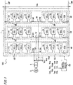
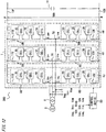
- FIG. 1 is a schematic configuration diagram of a power conversion device 100 according to Embodiment 1 of the present invention.
- FIG. 2 is a schematic configuration diagram of a two-terminal HVDC system configured using a plurality of the power conversion devices 100 according to Embodiment 1 of the present invention.
- the power conversion devices 100 of the present embodiment are denoted by 100A and 100B.
- the power conversion device 100 performs power conversion between DC and AC. As shown in FIG. 2 , the AC sides of the power conversion devices 100A, 100B are respectively connected to three-phase AC power supplies 9A, 9B which are AC grids. The DC sides of the power conversion devices 100A, 100B are connected to a DC grid formed by positive and negative DC lines 13P, 13N. Thus, a two-terminal high-voltage DC (HVDC: High Voltage Direct Current) system is formed as a power system that allows high-voltage DC power to be passed and received between the power conversion devices 100A, 100B.
- HVDC High Voltage Direct Current
- the power conversion device 100 includes a power converter 1 which is a main circuit, and a control device 50 for controlling the power converter 1.
- the AC side of the power converter 1 is connected to the three-phase AC power supply 9 via an interconnection transformer 8, and the DC side thereof is connected to the positive and negative DC lines 13P, 13N via DC terminals P, N.
- the phases of the power converter 1 are formed by phase arms (phase arms 4U, 4V, 4W).
- the plurality of phase arms 4U, 4V, 4W are formed by respectively connecting, in series, first arms 5U, 5V, 5W connected to the positive DC line 13P and second arms 6U, 6V, 6W connected to the negative DC line 13N.
- AC terminals 7U, 7V, 7W which are connection points between the first arms 5U, 5V, 5W and the second arms 6U, 6V, 6W are connected to AC lines for the respective phases.
- These three phase arms 4U, 4V, 4W are connected in parallel between the positive and negative DC lines 13P, 13N.
- the first arms 5U, 5V, 5W and the second arms 6U, 6V, 6W are each formed by a cell group including one or more converter cells (first converter cells 10, second converter cells 20) connected in series.
- Reactors 11U, 11V, 11W are connected in series to the first arms 5U, 5V, 5W.
- Reactors 12U, 12V, 12W are connected in series to the second arms 6U, 6V, 6W.
- the positions where the reactor 11 and the reactor 12 are provided may be any positions in the first arm 5 and the second arm 6.
- the reactor 11 and the reactor 12 may be collectively provided on only one of the first arm 5 side and the second arm 6 side.
- FIG. 3 is a configuration diagram of the first converter cell 10 having a half-bridge configuration and used for the first arm 5, according to Embodiment 1 of the present invention.
- the first converter cell 10 is composed of a first series body 23 and a DC capacitor 29 connected in parallel to the first series body 23.
- the first series body 23 has, in respective upper and lower arms, a plurality of (in this case, two) semiconductor switching elements 21s, 22s (hereinafter, simply referred to as switching elements) to which diodes 21d, 22d are connected in antiparallel.
- the DC capacitor 29 smooths DC voltage.
- the switching elements 21s, 22s are each formed from a self-turn-off switching element such as IGBT (Insulated Gate Bipolar Transistor) or GCT (Gate Commutated Turn-off Thyristor), and diodes 21d, 22d are respectively connected in antiparallel thereto, to form switches 21, 22.
- IGBT Insulated Gate Bipolar Transistor
- GCT Gate Commutated Turn-off Thyristor
- both terminals of the switching element 22s of the switch 22 are used as output ends, and the switching elements 21s, 22s are switched on/off.
- both-end voltage of the DC capacitor 29, and zero voltage in a state in which input/output terminals are short-circuited are output.
- FIG. 4 shows the configuration of the second converter cell 20 used for the second arm 6 according to Embodiment 1 of the present invention.
- the second converter cell 20 is composed of a first series body 35, a second series body 36 connected in parallel to the first series body, and a DC capacitor 39 for smoothing DC voltage.
- the first series body 35 has, in respective upper and lower arms, a plurality of (in this case, two) switching elements 31s, 32s to which diodes 31d, 32d are connected in antiparallel.
- the second series body 36 is configured such that one of upper and lower arms has a diode 33, and in the other arm, a switching element 34s to which a diode 34d is connected in antiparallel is connected in series.
- the diode 33 is provided in the upper arm.
- the switching elements 31s, 32s, 34s are each formed from a self-turn-off switching element such as IGBT or GCT, and the diodes 31d, 32d, 34d are connected in antiparallel thereto, to form switches 31, 32, 34.
- connection point between the switching elements 31s, 32s and the connection point between the diode 33 and the switching element 34s which are the respective intermediate connection points of the first series body 35 and the second series body 36, are used as output ends, and the switching elements 31s, 32s, 34s are switched on/off.
- same-polarity positive voltage almost equal to the magnitude of both-end voltage of the DC capacitor 39
- opposite-polarity negative voltage almost equal to the magnitude of the both-end voltage
- zero voltage in a state in which input/output terminals are short-circuited are output.
- the negative-polarity voltage can be output under the condition that current passing through the second converter cell 20 flows from an input/output terminal No to an input/output terminal Po, the switching element 32s is ON, and the switching elements 31s, 34s are OFF.
- the first converter cell 10 is not limited to the configuration shown in FIG. 3 as long as the first converter cell 10 is composed of a series body formed by switching elements, and a DC capacitor connected in parallel to the series body, and is configured to selectively output the voltage of the series capacitor through switching operation.
- the second converter cell 20 is not limited to the configuration shown in FIG. 4 as long as the second converter cell 20 is composed of a series body formed by a switching element and a diode, and a DC capacitor connected in parallel to the series body, and is configured to selectively output the voltage of the series capacitor through switching operation.
- all the converter cells composing the first arm 5 of the power converter 1 are the first converter cells 10 which have a half-bridge configuration and are capable of outputting positive voltage between both ends of the DC capacitor 29 and zero voltage.
- all the converter cells composing the second arm 6 of the power converter 1 are the second converter cells 20 which are capable of outputting positive voltage/negative voltage between both ends of the DC capacitor 39 and zero voltage.
- First arm currents ipu, ipv, ipw and second arm currents inu, inv, inw flowing through the first arms 5U, 5V, 5W and the second arms 6U, 6V, 6W of the power converter 1 are detected by current detectors (not shown) and then input to the control device 50.
- phase voltages Vsu, Vsv, Vsw of the three-phase AC power supply 9, DC voltage Vdc between the DC terminals P and N, and DC capacitor voltages Vcap of the first converter cell 10 and the second converter cell 20, are detected by voltage detectors (not shown) and then input to the control device 50.
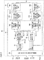
- FIG. 5 is a block diagram showing a configuration example of the control device 50 in the power conversion device 100 according to Embodiment 1 of the present invention.
- the control device 50 includes a voltage command value generation unit 51 and a PWM unit 52 formed from respective control systems.
- the control device 50 generates voltage command values V+*, V-* for the first arm 5 and the second arm 6, and on the basis of the voltage command values V+*, V-*, generates gate signals G for performing PWM control of the first converter cells 10 and the second converter cells 20, thereby controlling the power converter 1.
- the voltage command value generation unit 51 includes a normalization/calculation unit 59, a DC-AVR (Direct Current-Automatic Voltage Regulator)/DC-ACR (Direct Current-Automatic Current Regulator) control unit 53, a DC voltage command value calculation unit 54, an AC voltage control unit 55, a first arm voltage command value calculation unit 56A, a second arm voltage command value calculation unit 56B, a first-arm-side cell individual control unit 57A, and a second-arm-side cell individual control unit 57B.
- DC-AVR Direct Current-Automatic Voltage Regulator
- DC-ACR Direct Current-Automatic Current Regulator
- the normalization/calculation unit (hereinafter, referred to as conversion unit 59) converts the detected first arm currents (ipu, ipv, ipw), second arm currents (inu, inv, inw), phase voltages (Vsu, Vsv, Vsw), DC voltage Vdc, and DC capacitor voltage Vcap, to signals for use in the control.
- the DC-AVR/DC-ACR control unit (hereinafter, referred to as DC control unit 53) generates a DC voltage command value Kdc* for controlling DC voltage Vdc, on the basis of DC current Idc and DC voltage Vdc obtained through conversion by the conversion unit 59.
- the DC voltage command value calculation unit 54 calculates a DC voltage command value Vdc+* for the first arm 5 and a DC voltage command value Vdc-* for the second arm 6, on the basis of the DC voltage command value Kdc* received from the DC control unit 53.
- the AC voltage control unit 55 generates AC voltage command values Vac+, Vac- for the first arm 5 and the second arm 6, on the basis of AC voltage Vs, AC current lac, and DC capacitor voltage Vcap obtained through conversion by the conversion unit 59.
- the first arm voltage command value calculation unit 56A calculates a voltage command value V+* for the first arm 5 on the basis of the DC voltage command value Vdc+* and the AC voltage command value Vac+* respectively calculated by the DC voltage command value calculation unit 54 and the AC voltage control unit 55.
- the second arm voltage command value calculation unit 56B calculates a voltage command value V-+* for the second arm 6 on the basis of the DC voltage command value Vdc-* and the AC voltage command value Vac-*.
- the first-arm-side cell individual control unit 57A generates a first-arm-side cell voltage command value Vcell+* for controlling the voltage of each first converter cell 10 composing the first arm 5, on the basis of the voltage command value V+* calculated by the first arm voltage command value calculation unit 56A, and the DC capacitor voltage Vcap.
- the second-arm-side cell individual control unit 57B generates a second-arm-side cell voltage command value Vcell-* for controlling the voltage of each second converter cell 20 composing the second arm 6, on the basis of the voltage command value V-* and the DC capacitor voltage Vcap.
- the PWM unit 52 includes a first-arm-side PWM circuit unit 58A and a second-arm-side PWM circuit unit 58B.
- the first-arm-side PWM circuit unit 58A and the second-arm-side PWM circuit unit 58B generate gate signals G for performing PWM control of each of the first converter cells 10 and the second converter cells 20 in the first arm 5 and the second arm 6 for each phase, on the basis of the first-arm-side cell voltage command value Vcell+* and the second-arm-side cell voltage command value Vcell-*.
- the switching elements 21s, 22s in the first converter cell 10 and the switching elements 31s, 32s, 34s in the second converter cell 20 are drive-controlled.
- the output voltage of the power converter 1 is controlled to be a desired value.
- the voltage command value V+* for the first arm 5 is determined in accordance with the DC voltage command value Vdc+* calculated by the DC voltage command value calculation unit 54 and the AC voltage command value Vac+* calculated by the AC voltage control unit 55.
- the voltage command value V-* for the second arm 6 is determined in accordance with the DC voltage command value Vdc-* calculated by the DC voltage command value calculation unit 54 and the AC voltage command value Vac-* calculated by the AC voltage control unit 55. That is, the voltage command values V+*, V-* for the first arm 5 and the second arm 6 contain two components, i.e., a DC component and an AC component.
- each converter cell in the first arm 5 is the first converter cell 10 which has a half-bridge configuration and is capable of outputting positive voltage and zero voltage. Therefore, a voltage command value to be given to the first converter cell 10 in the first arm 5 is limited within a positive region. That is, the DC voltage command value Vdc+* contained in the voltage command value V+* for the first arm 5 is limited to a positive value. In addition, the maximum amplitude of the AC voltage command value Vac+* contained in the voltage command value V+* for the first arm 5 depends on the DC voltage command value Vdc+*.
- each converter cell in the second arm 6 is the second converter cell 20 which is capable of outputting positive voltage, negative voltage, and zero voltage as described above. Therefore, although depending on the polarity of current flowing in the second converter cell 20 in the second arm 6, a voltage command value to be given to the second converter cell 20 in the second arm 6 can have values in both positive and negative regions.
- both positive and negative values can be selected for the DC voltage command value Vdc-* contained in the voltage command value V-* for the second arm 6.
- the AC voltage command value Vac-* contained in the voltage command value V-* for the second arm 6 is set to have a polarity opposite to the AC voltage command value Vac+* for the first arm 5.
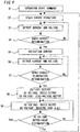
- FIG. 6 is a flowchart showing control operation of the power conversion device 100 according to Embodiment 1 of the present invention.
- FIG. 7 shows a route of short-circuit current ia flowing when short-circuit occurs between the DC terminals P and N.
- FIG. 8 shows waveforms of AC grid voltage, DC voltage Vdc, voltage of the first arm 5, and voltage of the second arm 6 in restart control of the power converter 1 according to Embodiment 1 of the present invention.
- step S1 When an operation start command for the power converter 1 is given (step S1), the control device 50 sets the operation mode of the power converter 1 to steady control, to start steady operation of the power converter 1. That is, the control device 50 fixes the switching element 34s of the second series body 36 of each second converter cell 20 in the second arm 6, in an ON state. Then, the control device 50 causes the switching elements 21s, 22s, 31s, 32s in the first series bodies 23, 35 of each first converter cell 10 and each second converter cell 20 to perform steady operations (step S2).
- control device 50 obtains DC current Idc flowing through the DC terminal P and DC voltage Vdc between the DC terminals P and N, by detection or calculation (step S3).
- the control device 50 determines whether or not short-circuit has occurred between the DC terminals P and N (DC lines 13P, 13N), on the basis of the DC current Idc and the DC voltage Vdc. For example, if the DC current Idc becomes overcurrent exceeding a set reference value and the DC voltage Vdc becomes almost zero, the control device 50 determines that short-circuit has occurred (step S4, YES).
- step S4 If it is determined in step S4 that short-circuit has not occurred (step S4, NO), the process returns to step S3 and the control device 50 repeats the short-circuit determination periodically.
- step S4 if it is determined in step S4 that short-circuit has occurred between the DC terminals P and N, the control device 50 switches the operation mode of the power converter 1 from steady control to protection control, and the power converter 1 starts protection operation (step S5). That is, the control device 50 controls all the switching elements 21s, 22s, 31s, 32s, 34s in each first converter cell 10 and each second converter cell 20 into an OFF state, thereby suppressing the short-circuit current ia.
- short-circuit current ia flows through a route indicated by an arrow in FIG. 7 .
- protection control of turning off all the switching elements 21s, 22s, 31s, 32s, 34s is performed.
- short-circuit current ia does not flow as long as the sum of the charge voltages of the DC capacitors 39 of the second converter cells 20 connected in the route of the short-circuit current ia is higher than voltage between the AC terminals 7.
- the number of the second converter cells 20 composing the second arm 6 is adjusted so as to satisfy the above condition, and therefore the short-circuit current ia can be suppressed.
- the switching elements 21s, 22s of each first converter cell 10 having a half-bridge configuration in the first arm 5 are turned off, and this is for reducing the influence of the switching operations on the AC terminals 7 and does not contribute to suppression of the short-circuit current ia.
- control device 50 obtains DC current Idc and DC voltage Vdc by detection or calculation (step S6).
- control device 50 determines whether or not the short-circuit between the DC terminals P and N has been eliminated, on the basis of the DC current Idc and the DC voltage Vdc (step S7).
- step S7 If it is determined in step S7 that the short-circuit state has continued (step S7, NO), the process returns to step S6 and the control device 50 repeats the short-circuit elimination determination periodically.
- step S7 if it is determined in step S7 that the short-circuit between the DC terminals P and N has been eliminated, the control device 50 switches the operation mode of the power converter 1 to restart control, and the power converter 1 initiates restart operation (step S8).
- the control device 50 performs control so that rated AC voltage Vac is output to the AC terminals 7U, 7V, 7W and zero voltage is output between the DC terminals P and N.
- the power converter 1 can output zero voltage between the DC terminals P and N if the DC voltage command value Vdc+* for the first arm 5 and the DC voltage command value Vdc-* for the second arm 6 are DC voltage command values having magnitudes equal to each other and polarities opposite to each other.
- +1/2Vdc is set as the DC voltage command value Vdc+* for the first arm 5
- -1/2Vdc is set as the DC voltage command value Vdc-* for the second arm 6.
- the control device 50 generates gate signals G based on the above voltage command values V+*, V-* and performs switching control of the switching elements 21s, 22s, 31s, 32s, 34 by PWM control. In this way, at the initiation of the restart control, the control device 50 outputs rated AC voltage Vac to the AC terminals 7 and outputs zero voltage between the DC terminals P and N.
- the control device 50 adds an adjustment voltage value ⁇ dc which is a minute DC voltage value, to the DC voltage command value Vdc-* for the second arm 6, in the DC voltage command value calculation unit 54.
- Vdc ⁇ t ⁇ Vdc ⁇ t ⁇ ⁇ t ⁇ + ⁇ dc
- ⁇ t is a cycle of addition of ⁇ dc.
- the voltage value of DC voltage Vdc output between the DC terminals P and N becomes a value obtained by multiplying the minute adjustment voltage value ⁇ dc with the number n of times of addition of the adjustment voltage value ⁇ dc.
- Vdc V ⁇ dc V ⁇ number n of times of addition
- the DC voltage command value Vdc-* for the second arm 6 is increased every addition cycle ( ⁇ t), so that the DC voltage command value Vdc-* for the second arm 6 gradually increases from the negative-polarity rated DC voltage command value (-1/2Vdc) to the positive-polarity rated DC voltage command value (+1/2Vdc).
- the DC voltage Vdc between the DC terminals P and N gradually increases so as to follow the voltage command values V+*, V-* which gradually increase in a ramp function shape from zero voltage to the rated voltage Vdc.
- control device 50 obtains the DC voltage Vdc by detection, and on the basis of the DC voltage Vdc, determines whether or not the voltage between the DC terminals P and N has reached the rated value (step S10).
- step S10 If it is determined in step S10 that the DC voltage Vdc has reached the rated value (step S10, YES), the control device 50 switches the operation mode to steady control, to start power transmission (step S2).
- step S10 If it is determined that the DC voltage Vdc has not reached the rated voltage (step S10, NO), the process returns to step S9 to add ⁇ dc to the DC voltage command value and then proceeds to step S10, whereby the rated value determination is repeated periodically.
- the second converter cells 20 capable of outputting negative-polarity voltage are used. Therefore, even if the voltage command value V-* for the second arm 6 as described above includes the negative-polarity rated DC voltage command value (-1/2Vdc), it is possible to perform output corresponding to this voltage command value V-*.
- FIG. 9 shows a route of negative-polarity current in caused to flow in the power converter 1 in restart control of the power converter 1 according to Embodiment 1 of the present invention.
- a stray impedance ZP of the DC line 13P connected to the DC terminal P is represented by a reactor 13P11, a resistor 13Pr1, a resistor 13Pr2, a reactor 13P12, and a capacitor 13Pc
- a stray impedance ZN of the DC line 13N connected to the DC terminal N is represented by a reactor 13N11, a resistor 13Nr1, a resistor 13Nr2, a reactor 13N12, and a capacitor 13Nc.
- the capacitors 13Pc, 13Nc which are stray capacitances are once discharged when short-circuit occurs between the DC terminals P and N.
- the control device 50 turns on the switching elements 32s and turns off the switching elements 31s, 34s in the second arm 6 so as to allow the second converter cell 20 to output negative-polarity voltage, i.e., so as to ensure a current route through which negative-polarity current in flows in the phase arm 4.
- the negative-polarity current in flows through: the reactor 13P11, the resistor 13Pr1, the capacitor 13Pc, and a ground 13Pg; a ground 13Ng, the capacitor 13Nc, the resistor 13Nr1, and the reactor 13N11 of the DC line 13N; and then the diode 33 and the switch 32 in each second converter cell 20. That is, the negative-polarity current in flows through each second arm 6 (in a direction from the second arm 6 to the first arm 5). Thus, the second converter cells 20 are enabled to output negative-polarity voltage in the restart control.
- control device 50 performs switching control of the second converter cells 20 so as to ensure a route through which the negative-polarity current in flows, using the impedances that the DC lines 13P, 13N have. In this way, DC voltage that gradually increases is output to the DC line 13P while the negative-polarity current in is caused to flow through the phase arm 4.
- step S1 to step S10 the control device 50 switches the operation mode from steady control to protection control when short-circuit between the DC terminals P and N is detected. Then, the control device 50 controls all the switching elements in the first converter cells 10 and the second converter cells 20 into an OFF state, thereby suppressing the short-circuit current ia.
- the control device 50 switches the operation mode from protection control to restart control. Then, the control device 50 raises the voltage between the DC terminals P and N from zero to the rated value in a ramp function shape with a predetermined slope, while performing rated output to the AC grid.
- the second converter cell 20 having the diode 33 in the upper arm of the second series body 36 is used as each converter cell used in the second arm 6 and capable of outputting negative-polarity voltage.
- the diode 33 is used, instead of a switching element, for the upper arm of the second series body 36 which is used as a route through which negative-polarity current in flows in the second converter cell 20, whereby noise at the time of driving switching elements is reduced.
- the control device 50 controls the switching elements 31s, 32s, 34s in each second converter cell 20 so as to ensure a route for negative-polarity current in flowing through each diode 33 in the phase arm 4.
- voltage is applied to the DC lines 13P, 13N and negative-polarity current in flows to the phase arm 4 in the power converter 1 via the stray impedances ZP, ZN.
- a converter cell having a diode in one of upper and lower arms can be used for the power converter 1.
- noise due to switching control of switching elements is reduced and change in the polarity of the negative-polarity current in is suppressed, whereby the power converter 1 of the power conversion device 100 can be accurately restarted.
- rated DC voltage Vdc is swiftly applied to the DC lines 13P, 13N, and the high-voltage direct current (HVDC) system can be operated in a more stable manner.
- the control load for the switching control in the control device 50 can be reduced.
- the first converter cells 10 having a half-bridge configuration are used, and in the second arm 6, the second converter cells 20 are used. Then, the number of the second converter cells 20, the capacitances of the DC capacitors, and the like are adjusted in order that short-circuit current ia can be suppressed by only the second converter cells 20 in the second arm 6.
- the converter cells in the first arm 5 do not need to have a function of suppressing the short-circuit current ia, and therefore the first arm 5 can be formed by only the first converter cells 10 having a half-bridge configuration.
- the number of semiconductor switching elements used in the power converter 1 is decreased, the device configuration is downsized, and the cost can be reduced.
- the first arm 5 is connected to the positive DC line 13P
- the second arm 6 is connected to the negative DC line 13N
- the first arm 5 may be connected to the negative DC line 13N
- the second arm 6 may be connected to the positive DC line 13P. That is, the second converter cells 20 capable of outputting the opposite-polarity voltage may be used for the arm connected to the positive DC line 13P, and the first converter cells 10 having a half-bridge configuration may be used for the arm connected to the negative DC line 13N.
- the first arm 5 and the second arm 6 may be both formed by only the second converter cells 20 without using the first converter cells 10 having a half-bridge configuration.
- the first arm 5 may be formed by the first converter cells 10 and the second converter cells 20 in a mixed manner.
- the number of the second converter cells 20 provided in the first arm 5 may be determined so that the second converter cells 20 the number of which enables suppression of the short-circuit current ia exist in the route of the short-circuit current ia.
- the AC terminals 7U, 7V, 7W which are the connection points between the first arms 5U, 5V, 5W and the second arms 6U, 6V, 6W are directly connected to the respective phase AC lines, whereby power is passed and received to and from the three-phase AC power supply 9.
- the power conversion device 100 is not limited to the above configuration.
- the first arm 5 and the second arm 6 are connected in series via a primary winding of a transformer and then connected to the respective phase AC lines via a secondary winding of the transformer, whereby power is passed and received to and from the three-phase AC power supply 9.
- a second converter cell 20a having the following configuration may be used.
- FIG. 10 shows the second converter cell 20a having a configuration different from the second converter cell 20 according to the present Embodiment 1.
- a switching element 37s to which a diode 37d is connected in antiparallel is provided in an upper arm of a second series body 36a.
- the switching element 37s is formed from a self-turn-off switching element such as IGBT or GCT, and the diode 37d is connected in antiparallel thereto, to form a switch 37.
- terminals at the connection point between the switching elements 31s, 32s and the connection point between the switching elements 37s, 34s, which are intermediate connection points of the first series body 35 and 36a, are used as output ends.
- the control device 50 performs switching of the switching elements 31s, 32s, 37s, 34s, thereby outputting, from the output ends, same-polarity positive voltage almost equal to the magnitude of both-end voltage of the DC capacitor 39, opposite-polarity negative voltage almost equal to the magnitude of the both-end voltage, and zero voltage in a state in which the output terminals are short-circuited with an element.
- control device 50 controls all the switching elements 31s, 32s, 37s, 34s in each second converter cell 20a into an OFF state, thereby suppressing short-circuit current ia.
- the control device 50 fixes the switching element 37s in an OFF state, to ensure a route for negative-polarity current in to flow through the flyback diode 37d and the switch 32.
- the switching element 37 being fixed in an OFF state as described above, noise due to switching control of the switching elements in the route through which the negative-polarity current in flows can be reduced.
- control device 50 may fix the switching element 37s in an OFF state and perform switching control of the switching elements 31s, 32s, 34s.
- the switching element 37s since the switching element 37s is always fixed in an OFF state, a small-sized switching element 37s having a small rated current can be used, and deterioration of the switching element 37s can be prevented.
- the control device 50 provides the second arm 6 with the voltage command value V+* including a rated AC voltage command value and a voltage command value that gradually increases from a negative-polarity rated DC voltage command value to a positive-polarity rated DC voltage command value.
- the control device 50 provides the first arm 5 with a rated AC voltage command value and a positive-polarity rated DC voltage command value.
- the DC voltage Vdc changes in a range of "0 V to rated voltage V".
- the change range of the DC voltage Vdc is not limited to the above range.
- Embodiment 2 of the present invention will be described focusing on difference from the above Embodiment 1.
- the same parts as those in the above Embodiment 1 are denoted by the same reference characters and the description thereof is omitted.
- FIG. 11 is a flowchart showing control operation of a power conversion device according to Embodiment 2.
- the present embodiment is different from Embodiment 1 in that step S211, step S212, and step S213 are newly provided subsequently to step S9 and step S10 described in Embodiment 1.
- the control device 50 adds the adjustment voltage value ⁇ dc which is a minute DC voltage value, to the DC voltage command value Vdc-* for the second arm 6, thereby raising the DC voltage Vdc. Then, the control device 50 determines whether or not the DC voltage Vdc between the DC terminals P and N has reached the rated value.
- the control device 50 detects the voltage Vcap of each DC capacitor 29, 39 in the power converter 1 and determines whether or not the voltage Vcap is out of a predetermined voltage value range (step S211).
- step S211, NO If the control device 50 does not detect imbalance of the voltages Vcap of the DC capacitors 29, 39 (step S211, NO), the process returns to step S9.
- the control device 50 detects imbalance of the voltages Vcap of the DC capacitors 29, 39, the control device 50 further adds a minute adjustment voltage ⁇ dc2 to the voltage command value V-* for the second arm 6, in addition to the adjustment voltage value ⁇ dc.Thus, the speed of gradual increase of the DC voltage Vdc on the DC line 13P becomes faster than the speed of gradual increase at the time of the imbalance detection, whereby a time period required for restart of the power converter 1 is shortened. In this way, the DC voltage Vdc of the DC line 13P is raised immediately and the negative-polarity current in is increased immediately, whereby influence of noise on the negative-polarity current in is suppressed.
- control device 50 obtains the DC voltage Vdc by detection, and on the basis of the DC voltage Vdc, determines whether or not the voltage between the DC terminals P and N has reached the rated value (step S213).
- step S213, NO If it is determined that the DC voltage Vdc has not reached the rated voltage (step S213, NO), the process returns to step S212 to add the adjustment voltage value ⁇ dc and the adjustment voltage value ⁇ dc2 to the DC voltage command value, and the rated value determination is repeated periodically.
- the power conversion device of the present Embodiment 2 configured as described above provides the same effects as in the above Embodiment 1, and thus it becomes possible to swiftly start up the power converter 1 in accordance with the voltage command value.
- the adjustment voltage value ⁇ dc and the adjustment voltage value ⁇ dc2 to be added to the DC voltage command value Vdc+ can be set to any values within such a range as not to cause overvoltage on the DC line 13P.
- Embodiment 3 of the present invention will be described focusing on difference from the above Embodiment 1.
- the same parts as those in the above Embodiment 1 are denoted by the same reference characters and the description thereof is omitted.
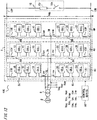
- FIG. 12 is a schematic configuration diagram of a power conversion device 300 according to Embodiment 3 of the present invention.
- the present embodiment is different from Embodiment 1 in that, as the impedance between the DC lines 13P, 13N, a capacitance 14 is connected between the DC lines 13P, 13N.
- negative-polarity current in is caused to flow through the phase arm 4 of the power converter 1, using the stray impedances ZP, ZN that the DC lines 13P, 13N have.
- the capacitance 14 for causing the negative-polarity current in to flow is connected between the DC lines 13P, 13N.
- the power conversion device of the present Embodiment 3 configured as described above provides the same effects as in the above Embodiment 1, and thus it becomes possible to swiftly start up the power converter 1 in accordance with the voltage command value.
- the value of the capacitance 14 may be determined on the basis of the speed of gradual increase of the DC voltage Vdc on the DC line 13P in the restart control.
- Embodiment 4 of the present invention will be described focusing on difference from the above Embodiment 1.
- the same parts as those in the above Embodiment 1 are denoted by the same reference characters and the description thereof is omitted.
- FIG. 13 is a schematic configuration diagram of a power conversion device 400 according to Embodiment 4 of the present invention.
- FIG. 14 is a flowchart showing control operation of the power conversion device according to Embodiment 4.
- step S414 is newly provided between step S7 and step S8 described in Embodiment 1 and step S415 is newly provided subsequently to step S10.
- step S10 is newly provided subsequently to step S10.
- the device 15 is used as a current route for negative-polarity current in at the time of restart control, but is not used in steady control and protection control of the power converter 1. Therefore, in steady control and protection control of the power converter 1, the switch 15s is turned off so that current does not flow into the resistor 15r.
- Control by the control device 50 using the device 15 will be described with reference to FIG. 14 .
- control device 50 performs protection control for suppressing short-circuit current ia, and then determines whether or not the short-circuit between the DC terminals P and N has been eliminated.
- step S7 if it is determined in step S7 that the short-circuit between the DC terminals P and N has been eliminated, the control device 50 causes the switch 15s of the device 15 to be closed (step S414).
- the control device 50 adds the adjustment voltage value ⁇ dc which is a minute DC voltage value, to the DC voltage command value Vdc-* for the second arm 6, thereby raising the DC voltage Vdc, and determines whether or not the voltage between the DC terminals P and N has reached the rated value.
- negative-polarity current in is caused to flow through the phase arm 4 of the power converter 1, using the stray impedances ZP, ZN that the DC lines 13P, 13N have.
- the switch 15s in the restart control, the switch 15s is closed, whereby negative-polarity current in is caused flow via the resistor 15r.
- control device 50 determines in step S10 that the voltage between the DC terminals P and N has reached into the rated voltage value range, the control device 50 causes the switch 15s of the device 15 to be opened (step S415), switches the operation mode to steady control, and starts power transmission.
- the power conversion device of the present Embodiment 4 configured as described above provides the same effects as in the above Embodiment 1, and thus it becomes possible to swiftly start up the power converter 1 in accordance with the voltage command value.
- the resistor 15r is used.
- another impedance such as a reactor or a capacitor may be used.
- the resistance value of the resistor 15r may be determined on the basis of the speed of gradual increase of the DC voltage Vdc on the DC line 13P in the restart control.
- FIG. 15 is a schematic configuration diagram of a three-terminal HVDC system 570 configured using a plurality of power conversion devices, according to Embodiment 5 of the present invention.
- the power conversion devices 100 described in Embodiment 1 are denoted by 100A, 100B, and 100C.
- the AC sides of the power conversion devices 100A, 100B, 100C are connected to three-phase AC power supplies 9A, 9B, 9C, respectively.
- the DC terminals P and N on the DC sides of the power conversion devices 100A, 100B, 100C are connected to each other via DC lines 13PA, 13NA, 13PB, 13NB, 13PC, 13NC.
- each of the power conversion devices 100A, 100B, 100C switches the operation mode from steady control to protection control.
- the power conversion device 100A When having detected elimination of the short-circuit, the power conversion device 100A switches the operation mode of the power conversion device 100A from protection control to restart control, and raises the DC terminal voltage in a ramp function shape from zero to the rated value while performing rated output to the three-phase AC power supply 9A. Thereafter, the power conversion devices 100B, 100C are sequentially started up to start power transmission.
- each power conversion device 100A, 100B, 100C can also operate as a STATCOM for supplying reactive power to the three-phase AC power supply 9A, 9B, 9C in protection control.
- the number of DC terminals may be four or more, and the number of terminals of the DC lines and the connection manner thereof are not limited to those shown in FIG. 15 .
- FIG. 16 is a schematic configuration diagram of a two-terminal HVDC system 670 configured using two power conversion devices, according to Embodiment 6 of the present invention.
- the two-terminal HVDC system 670 as a power conversion system includes a power conversion device 600A, a power conversion device 600B, and a monitoring device 17.
- the power conversion device 600A is provided with second switches 16PA, 16NA connected to DC terminals P, N on the DC side.
- the power conversion device 600B is provided with second switches 16PB, 16NB connected to DC terminals P, N on the DC side.
- the DC terminals P, N of the power conversion device 600A are connected to DC lines 13P, 13N via the second switches 16PA, 16NA.
- the DC terminals P, N of the power conversion device 600B are connected to the DC lines 13P, 13N via the second switches 16PB, 16NB.
- the AC side of the power conversion device 600A is connected to a three-phase AC power supply 9A, and the AC side of the power conversion device 600B is connected to a three-phase AC power supply 9B.
- the monitoring device 17 constantly monitors voltage or current of the DC lines 13P, 13N, the operation states of the power conversion devices 600A, 600B, and the open/close states of the second switches 16PA, 16NA, 16PB, 16NB. Such information monitored by the monitoring device 17 is constantly transmitted to the power conversion devices 600A, 600B.
- control devices 50A, 50B of the power conversion devices 600A, 600B detect the short-circuit and switches their operation modes from steady control to protection control. At the same time, the control devices 50A, 50B cause the switches 16PA, 16NA, 16PB, 16NB to be opened, to disconnect the power conversion devices 600A, 600B from the short-circuited route.
- control devices 50A, 50B may be performed on the basis of the value of the DC current Idc as described in Embodiment 1.
- the control devices 50A, 50B may detect the short-circuit on the basis of monitored information about voltage or current of the DC lines 13P, 13N transmitted from the monitoring device 17.
- the control device 50A of the power conversion device 600A causes the second switches 16PA, 16NA to be closed.
- the control device 50B of the power conversion device 600B keeps the second switches 16PB, 16NB in an opened state.
- control device 50A of the power conversion device 600A determines that the second switches 16PB, 16NB provided to the power conversion device 600B are in an opened state, on the basis of monitored information about the open/close states of the second switches 16PB, 16NB transmitted from the monitoring device 17. Then, after the determination, the control device 50A of the power conversion device 600A switches the operation mode of the power converter 1 of the power conversion device 600A from protection control to restart control.
- the control device 50A of the power conversion device 600A causes negative-polarity current in to flow through the phase arm 4 of the power converter 1 of the power conversion device 600A, thereby raising the voltage between the DC terminals P, N in a ramp function shape from zero to the rated value.
- the power conversion device 600B is continuing protection control.
- control device 50B of the power conversion device 600B detects that the short-circuit has been eliminated and the power conversion device 600A has been restarted, on the basis of monitored information about the operation state of the power conversion device 600A and monitored information about voltage or current of the DC lines 13P, 13N, which are transmitted from the monitoring device 17. Then, the control device 50B of the power conversion device 600B switches the operation mode of the power converter 1 of the power conversion device 600B to restart control, and causes the second switches 16PB, 16NB to be closed.
- the power conversion devices 600A, 600B obtain voltage or current of the DC lines 13P, 13N, the operation states of the power conversion devices 600A, 600B, and the open/close states of the second switches 16PA, 16NA, 16PB, 16NB, from the monitoring device 17.
- the configuration is not limited to the above one.
- a sensor may be provided which is capable of monitoring voltage or current of the second DC lines 13P, 13N even after the power conversion device 600A is disconnected from the second DC lines 13P, 13N by the second switches 16PA, 16NA.
- the power conversion devices 600A, 600B may have respective transmission/reception units for the operation states.
- the power conversion device 600B performs restart control after the power conversion device 600A performs restart control.
- the power conversion device that has priority to perform restart control may be optionally selected and set, and this setting information may be stored in the control devices of the respective power conversion devices.
- the control device 50A of the power conversion device 600A performs restart control after determining that the second switches 16PB, 16NB provided to the power conversion device 600B are in an opened state. Therefore, during restart control of the power conversion device 600A, the power conversion device 600B is disconnected from the DC line 13P, 16N by the switches 16PB, 16NB. Thus, current does not flow into the power conversion device 600B when the power conversion device 600A performs restart control, whereby the power conversion device 600A can perform stable restart control.
Claims (14)
- Dispositif de conversion de puissance comprenant :- un convertisseur de puissance (1) incluant une pluralité de branches de phase (4U, 4V, 4W) dans lequel une première branche (5U, 5V, 5W) et une seconde branche (6U, 6V, 6W) pour chacune des phases sont connectées en série l'une à l'autre, la pluralité de branches de phase (4U, 4V, 4W) étant connectées en parallèle entre des lignes en courant continu (CC) positive et négative, le convertisseur de puissance (1) étant configuré pour exécuter une conversion de puissance entre un courant alternatif (CA) triphasé et un courant continu (CC) ; et- un dispositif de commande (50, 50A, 50B) qui est configuré pour générer des valeurs d'ordre de tension respectives pour la première branche (5U, 5V, 5W) et la seconde branche (6U, 6V, 6W) et pour exécuter une commande pilote du convertisseur de puissance (1) sur la base des valeurs d'ordre de tension,
dans lequel
la première branche (5U, 5V, 5W) et la seconde branche (6U, 6V, 6W) incluent chacune une cellule de convertisseur (10, 20, 20a) composée d'un premier corps en série (23, 35) ayant des éléments de commutation semi-conducteurs (21s, 22s, 31s, 32s) à la fois dans la branche supérieure et dans la branche inférieure ; et d'un condensateur CC (29, 39) connecté en parallèle au premier corps en série (23, 35),
la cellule de convertisseur (20, 20a) dans la seconde branche (6U, 6V, 6W) est une seconde cellule de convertisseur (20, 20a) formée en connectant le condensateur CC (39), le premier corps en série (23, 35), et un second corps en série (36, 36a) en parallèle, le second corps en série (36, 36a) ayant un élément de commutation semi-conducteur (34s) dans une branche parmi la branche supérieure et la branche inférieure et une diode (33, 37d) dans l'autre branche, la seconde cellule de convertisseur (20, 20a) étant configurée pour sortir des tensions de polarité positive et de polarité négative correspondant à une amplitude de tension aux deux extrémités du condensateur CC (39),
quand un court-circuit entre les lignes CC est détecté, le dispositif de commande (50, 50A, 50B) est configuré pour exécuter une commande de protection pour désactiver les éléments de commutation semi-conducteurs (21s, 22s, 31s, 32s, 34s, 37s) dans le convertisseur de puissance (1), et caractérisé en ce que
quand une élimination du court-circuit entre les lignes CC est détectée, le dispositif de commande (50, 50A, 50B) est configuré pour exécuter un redémarrage de commande du convertisseur de puissance (1) et pour donner une valeur d'ordre de tension, incluant une valeur d'ordre de tension CC de polarité positive, vers la cellule de convertisseur (10) dans la première branche (5U, 5V, 5W), et pour donner une valeur d'ordre de tension, incluant une valeur d'ordre de tension CC qui augmente graduellement depuis une polarité négative jusqu'à une polarité positive, vers la seconde cellule de convertisseur (20, 20a) dans la seconde branche (6U, 6V, 6W), sortant ainsi une tension CC qui augmente graduellement, vers les lignes CC, tout en amenant un courant de polarité négative à s'écouler à travers la diode (33, 37d) pour s'écouler jusqu'à la branche de phase (4U, 4V, 4W), en utilisant une impédance (ZP, ZN) qu'ont les lignes CC. - Dispositif de conversion de puissance selon la revendication 1,
dans lequel le second corps en série (36a) a un élément de commutation semi-conducteur (37s) auquel la diode (37d) est connectée en parallèle, dans l'autre, et dans la commande de redémarrage, le dispositif de commande (50, 50A, 50B) est configuré pour fixer l'élément de commutation semi-conducteur (37s) de l'autre dans le second corps en série (36a), dans un état d'arrêt OFF. - Dispositif de conversion de puissance selon la revendication 1 ou 2, dans lequel, dans la commande de redémarrage, quand une élimination du court-circuit entre les lignes CC est détectée, le dispositif de commande (50, 50A 50B) est configuré pour donner une valeur d'ordre de tension, incluant une valeur d'ordre de tension CA nominale et une valeur d'ordre de tension CC nominale de polarité positive, vers la cellule de convertisseur (10) dans la première branche (5U, 5V, 5W), et pour donner une valeur d'ordre de tension, incluant une valeur d'ordre de tension CA nominale et une valeur d'ordre de tension CC qui augmente graduellement depuis une valeur d'ordre de tension CC nominale de polarité négative jusqu'à une valeur d'ordre de tension CC nominale de polarité positive, vers la seconde cellule de convertisseur (20, 20a) dans la seconde branche (6U, 6V, 6W).
- Dispositif de conversion de puissance selon l'une quelconque des revendications 1 à 3,
dans lequel, dans la commande de redémarrage, quand il est détecté qu'une tension du condensateur CC (39) dans la seconde cellule de convertisseur (20, 20a) est en dehors d'une plage de valeurs de tension prédéterminée, le dispositif de commande (50, 50A, 50B) est configuré pour ajuster une valeur d'ordre de tension pour la seconde cellule de convertisseur (20, 20a) dans la seconde branche (6U, 6V, 6W) de sorte qu'une vitesse d'augmentation graduelle de tension CC sur les lignes CC devient plus rapide que celle à un moment de la détection. - Dispositif de conversion de puissance selon l'une quelconque des revendications 1 à 4,
dans lequel l'impédance (ZP, ZN) est une impédance parasite entre les lignes CC et une terre. - Dispositif de conversion de puissance selon l'une quelconque des revendications 1 à 5,
dans lequel une capacité (14) comme étant l'impédance (ZP, ZN) est prévue entre les lignes CC positive et négative, et
dans la commande de redémarrage, le dispositif de commande (50, 50A, 50B) est configuré pour amener le courant de polarité négative à s'écouler jusque dans la branche de phase (4U, 4V, 4W) via la capacité (14). - Dispositif de conversion de puissance selon l'une quelconque des revendications 1 à 6,
dans lequel une résistance (15r) comme étant l'impédance (ZP, ZN) et un premier commutateur (15s) connecté en série à la résistance sont prévus entre les lignes CC positive et négativs, et
quand une élimination du court-circuit entre les lignes CC est détectée, le dispositif de commande (50, 50A, 50B) est configuré pour exécuter la commande de redémarrage après avoir amené le premier commutateur (15s) à se fermer, et avoir amené le premier commutateur (15s) à s'ouvrir après qu'une tension des lignes CC a atteint une plage de valeurs de tension nominale. - Dispositif de conversion de puissance selon l'une quelconque des revendications 1 à 7,
dans lequel toutes les cellules de convertisseur (10) dans la première branche (5U, 5V, 5W) sont des premières cellules de convertisseur (10) formées chacune en connectant le condensateur CC (29) et le premier corps en série (23) en parallèle et ayant une configuration en demi-pont. - Dispositif de conversion de puissance selon l'une quelconque des revendications 1 à 7,
dans lequel toutes les cellules de convertisseur (20, 20a) dans la première branche (5U, 5V, 5W) sont les secondes cellules de convertisseur (20, 20a). - Dispositif de conversion de puissance selon l'une quelconque des revendications 1 à 7,
dans lequel la première branche (5U, 5V, 5W) est composée d'une première cellule de convertisseur (10) formée en connectant le condensateur CC (29) et le premier corps en série (23) en parallèle et ayant une configuration en demi-pont, et de la seconde cellule de convertisseur (20, 20a). - Dispositif de conversion puissance selon l'une quelconque des revendications 1 à 10,
dans lequel la somme des tensions de charge des condensateurs CC (39) des secondes cellules de convertisseur (20, 20a) connectées dans un itinéraire de courant de court-circuit du convertisseur de puissance (1), quand les lignes CC sont court-circuitées, est supérieure à la tension entre les lignes CA du convertisseur de puissance (1). - Dispositif de conversion de puissance selon la revendication 2,
dans lequel, dans une commande constante du convertisseur de puissance (1), le dispositif de commande (50, 50A, 50B) est configuré pour fixer l'élément de commutation semi-conducteur (37s) de l'autre dans le second corps en série (36a), dans un état d'arrêt OFF. - Système de puissance comprenant une pluralité des dispositifs de conversion de puissance (600A, 600B) selon l'une quelconque des revendications 1 à 12,
dans lequel les lignes CC des convertisseurs de puissance (1) des dispositifs de conversion de puissance (600A, 600B) sont connectées les unes aux autres. - Système de puissance selon la revendication 1 à 13,
dans lequel la pluralité de dispositifs de conversion de puissance (600A, 600B) sont chacun dotés d'un second commutateur (16PA, 16NA, 16PB, 16NB) connecté à une borne CC sur un côté CC du convertisseur de puissance (1), et sont connectés aux lignes CC via les seconds commutateurs (16PA, 16NA, 16PB, 16NB),
quand un court-circuit entre les lignes CC est détecté, la pluralité de dispositifs de conversion puissance (600A, 600B) sont configurés pour amener le second commutateur respectif (16PA, 16NA, 16PB, 16NB) à s'ouvrir, et pour exécuter la commande de protection, et
quand une élimination du court-circuit entre les lignes CC est détectée, un dispositif prédéterminé parmi la pluralité de dispositifs de conversion de puissance (600A, 600B) est configuré pour amener le second commutateur prévu sur le dispositif de conversion de puissance prédéterminé (600A, 600B) à se fermer, et après qu'il est déterminé que le second commutateur prévu sur l'autre dispositif de conversion de puissance (600A, 600B) est dans un état ouvert, le dispositif de conversion de puissance prédéterminé (600A, 600B) est configuré pour exécuter la commande de redémarrage.
Applications Claiming Priority (2)
| Application Number | Priority Date | Filing Date | Title |
|---|---|---|---|
| JP2016178473 | 2016-09-13 | ||
| PCT/JP2017/021147 WO2018051587A1 (fr) | 2016-09-13 | 2017-06-07 | Appareil de conversion de puissance et système électrique |
Publications (3)
| Publication Number | Publication Date |
|---|---|
| EP3514941A1 EP3514941A1 (fr) | 2019-07-24 |
| EP3514941A4 EP3514941A4 (fr) | 2019-10-09 |
| EP3514941B1 true EP3514941B1 (fr) | 2020-12-09 |
Family
ID=61619137
Family Applications (1)
| Application Number | Title | Priority Date | Filing Date |
|---|---|---|---|
| EP17850494.0A Active EP3514941B1 (fr) | 2016-09-13 | 2017-06-07 | Appareil de conversion de puissance et système électrique |
Country Status (4)
| Country | Link |
|---|---|
| US (1) | US10483871B2 (fr) |
| EP (1) | EP3514941B1 (fr) |
| JP (1) | JP6526344B2 (fr) |
| WO (1) | WO2018051587A1 (fr) |
Families Citing this family (14)
| Publication number | Priority date | Publication date | Assignee | Title |
|---|---|---|---|---|
| KR101923135B1 (ko) * | 2016-12-26 | 2018-11-28 | 효성중공업 주식회사 | 모듈러 멀티레벨 컨버터 시스템 |
| DE102017202204A1 (de) * | 2017-02-13 | 2018-08-16 | Siemens Aktiengesellschaft | Umrichteranordnung |
| EP3621193A1 (fr) * | 2018-09-06 | 2020-03-11 | ABB Schweiz AG | Fonction de mode de défaillance de court-circuit stable artificiel à l'aide de modules parallèles pour chaque fonction de commutation |
| EP3654510A1 (fr) * | 2018-11-19 | 2020-05-20 | Maschinenfabrik Reinhausen GmbH | Précharge d'un convertisseur multiniveaux modulairemodulaires à plusieurs niveaux |
| WO2020108736A1 (fr) * | 2018-11-27 | 2020-06-04 | Abb Schweiz Ag | Agencement de statcom sans réactances de phases |
| JP6545426B1 (ja) * | 2018-12-25 | 2019-07-17 | 三菱電機株式会社 | 電力変換装置 |
| EP3905504A4 (fr) * | 2018-12-25 | 2021-12-15 | Mitsubishi Electric Corporation | Dispositif de conversion de puissance |
| US11171575B2 (en) * | 2019-04-22 | 2021-11-09 | The Regents Of The University Of California | Modular multilevel converter topologies |
| WO2021005792A1 (fr) * | 2019-07-11 | 2021-01-14 | 三菱電機株式会社 | Dispositif de conversion de puissance électrique |
| WO2021024463A1 (fr) * | 2019-08-08 | 2021-02-11 | 三菱電機株式会社 | Dispositif de conversion de puissance |
| EP3780366A1 (fr) * | 2019-08-13 | 2021-02-17 | Vestas Wind Systems A/S | Hacheur cc pour cellule mmc avec résistance de hacheur intégré |
| CN112583244B (zh) * | 2019-09-29 | 2021-11-09 | 国创移动能源创新中心(江苏)有限公司 | 电力电子变压器系统直流母线电容的均压控制装置和方法 |
| JP6771707B1 (ja) * | 2020-03-11 | 2020-10-21 | 三菱電機株式会社 | 電力変換装置 |
| EP4262079A4 (fr) * | 2020-12-09 | 2024-01-17 | Mitsubishi Electric Corp | Dispositif de conversion d'énergie |
Family Cites Families (5)
| Publication number | Priority date | Publication date | Assignee | Title |
|---|---|---|---|---|
| CN101548461B (zh) * | 2006-12-08 | 2012-12-12 | 西门子公司 | 在电压中间电路变流器中用于控制直流侧的短路的半导体保护元件 |
| JP5894777B2 (ja) | 2011-12-07 | 2016-03-30 | 株式会社日立製作所 | 電力変換装置 |
| WO2015098146A1 (fr) * | 2013-12-24 | 2015-07-02 | 三菱電機株式会社 | Dispositif de conversion de puissance |
| CN104300569B (zh) * | 2014-09-29 | 2016-04-20 | 华中科技大学 | 基于混合型mmc的hvdc直流侧短路故障穿越和恢复方法 |
| DE102015109466A1 (de) * | 2015-06-15 | 2016-12-15 | Ge Energy Power Conversion Technology Limited | Stromrichter-Submodul mit Kurzschlusseinrichtung und Stromrichter mit diesem |
-
2017
- 2017-06-07 JP JP2018539524A patent/JP6526344B2/ja active Active
- 2017-06-07 EP EP17850494.0A patent/EP3514941B1/fr active Active
- 2017-06-07 US US16/311,872 patent/US10483871B2/en active Active
- 2017-06-07 WO PCT/JP2017/021147 patent/WO2018051587A1/fr active Application Filing
Also Published As
| Publication number | Publication date |
|---|---|
| JPWO2018051587A1 (ja) | 2019-01-17 |
| JP6526344B2 (ja) | 2019-06-05 |
| US20190207533A1 (en) | 2019-07-04 |
| EP3514941A1 (fr) | 2019-07-24 |
| WO2018051587A1 (fr) | 2018-03-22 |
| EP3514941A4 (fr) | 2019-10-09 |
| US10483871B2 (en) | 2019-11-19 |
Similar Documents
| Publication | Publication Date | Title |
|---|---|---|
| EP3514941B1 (fr) | Appareil de conversion de puissance et système électrique | |
| US10110110B2 (en) | Power conversion device | |
| JP6207730B2 (ja) | 直流送電電力変換装置および直流送電電力変換方法 | |
| EP2467928B1 (fr) | Alimentation électrique triphasée secourue à grande puissance | |
| US9608511B2 (en) | Method for charging modular multilevel converter | |
| EP3324531B1 (fr) | Dispositif de conversion de puissance | |
| US9960709B2 (en) | Power conversion device | |
| EP2587620B1 (fr) | Circuit d'équilibrage pour bus CC | |
| US10128741B2 (en) | Power conversion device | |
| EP3285388B1 (fr) | Dispositif de conversion de puissance électrique | |
| EP3285380B1 (fr) | Équilibrage de tension pour des convertisseurs de source de tension | |
| JPWO2019215842A1 (ja) | 電力変換装置 | |
| CA2405192C (fr) | Convertisseur de puissance | |
| US20180019685A1 (en) | Power converter | |
| US11716008B2 (en) | Power conversion device | |
| WO2024061964A1 (fr) | Précharge de filtre actif pour un convertisseur pourvu de cellules de filtre actif | |
| WO2020030245A1 (fr) | Procédé de commande d'un mmc |
Legal Events
| Date | Code | Title | Description |
|---|---|---|---|
| STAA | Information on the status of an ep patent application or granted ep patent |
Free format text: STATUS: THE INTERNATIONAL PUBLICATION HAS BEEN MADE |
|
| PUAI | Public reference made under article 153(3) epc to a published international application that has entered the european phase |
Free format text: ORIGINAL CODE: 0009012 |
|
| STAA | Information on the status of an ep patent application or granted ep patent |
Free format text: STATUS: REQUEST FOR EXAMINATION WAS MADE |
|
| 17P | Request for examination filed |
Effective date: 20190307 |
|
| AK | Designated contracting states |
Kind code of ref document: A1 Designated state(s): AL AT BE BG CH CY CZ DE DK EE ES FI FR GB GR HR HU IE IS IT LI LT LU LV MC MK MT NL NO PL PT RO RS SE SI SK SM TR |
|
| AX | Request for extension of the european patent |
Extension state: BA ME |
|
| A4 | Supplementary search report drawn up and despatched |
Effective date: 20190909 |
|
| RIC1 | Information provided on ipc code assigned before grant |
Ipc: H02M 7/49 20070101AFI20190903BHEP Ipc: H02M 7/483 20070101ALI20190903BHEP Ipc: H02M 7/797 20060101ALI20190903BHEP Ipc: H02M 1/00 20060101ALN20190903BHEP Ipc: H02M 1/32 20070101ALN20190903BHEP |
|
| DAV | Request for validation of the european patent (deleted) | ||
| DAX | Request for extension of the european patent (deleted) | ||
| GRAP | Despatch of communication of intention to grant a patent |
Free format text: ORIGINAL CODE: EPIDOSNIGR1 |
|
| STAA | Information on the status of an ep patent application or granted ep patent |
Free format text: STATUS: GRANT OF PATENT IS INTENDED |
|
| RIC1 | Information provided on ipc code assigned before grant |
Ipc: H02M 7/483 20070101ALI20200528BHEP Ipc: H02M 1/00 20060101ALN20200528BHEP Ipc: H02M 1/32 20070101ALN20200528BHEP Ipc: H02M 7/797 20060101ALI20200528BHEP Ipc: H02M 7/49 20070101AFI20200528BHEP |
|
| INTG | Intention to grant announced |
Effective date: 20200619 |
|
| GRAS | Grant fee paid |
Free format text: ORIGINAL CODE: EPIDOSNIGR3 |
|
| GRAA | (expected) grant |
Free format text: ORIGINAL CODE: 0009210 |
|
| STAA | Information on the status of an ep patent application or granted ep patent |
Free format text: STATUS: THE PATENT HAS BEEN GRANTED |
|
| AK | Designated contracting states |
Kind code of ref document: B1 Designated state(s): AL AT BE BG CH CY CZ DE DK EE ES FI FR GB GR HR HU IE IS IT LI LT LU LV MC MK MT NL NO PL PT RO RS SE SI SK SM TR |
|
| REG | Reference to a national code |
Ref country code: GB Ref legal event code: FG4D |
|
| REG | Reference to a national code |
Ref country code: AT Ref legal event code: REF Ref document number: 1344408 Country of ref document: AT Kind code of ref document: T Effective date: 20201215 Ref country code: CH Ref legal event code: EP |
|
| REG | Reference to a national code |
Ref country code: DE Ref legal event code: R096 Ref document number: 602017029433 Country of ref document: DE |
|
| REG | Reference to a national code |
Ref country code: IE Ref legal event code: FG4D |
|
| REG | Reference to a national code |
Ref country code: SE Ref legal event code: TRGR |
|
| PG25 | Lapsed in a contracting state [announced via postgrant information from national office to epo] |
Ref country code: FI Free format text: LAPSE BECAUSE OF FAILURE TO SUBMIT A TRANSLATION OF THE DESCRIPTION OR TO PAY THE FEE WITHIN THE PRESCRIBED TIME-LIMIT Effective date: 20201209 Ref country code: RS Free format text: LAPSE BECAUSE OF FAILURE TO SUBMIT A TRANSLATION OF THE DESCRIPTION OR TO PAY THE FEE WITHIN THE PRESCRIBED TIME-LIMIT Effective date: 20201209 Ref country code: NO Free format text: LAPSE BECAUSE OF FAILURE TO SUBMIT A TRANSLATION OF THE DESCRIPTION OR TO PAY THE FEE WITHIN THE PRESCRIBED TIME-LIMIT Effective date: 20210309 Ref country code: GR Free format text: LAPSE BECAUSE OF FAILURE TO SUBMIT A TRANSLATION OF THE DESCRIPTION OR TO PAY THE FEE WITHIN THE PRESCRIBED TIME-LIMIT Effective date: 20210310 |
|
| REG | Reference to a national code |
Ref country code: AT Ref legal event code: MK05 Ref document number: 1344408 Country of ref document: AT Kind code of ref document: T Effective date: 20201209 |
|
| PG25 | Lapsed in a contracting state [announced via postgrant information from national office to epo] |
Ref country code: BG Free format text: LAPSE BECAUSE OF FAILURE TO SUBMIT A TRANSLATION OF THE DESCRIPTION OR TO PAY THE FEE WITHIN THE PRESCRIBED TIME-LIMIT Effective date: 20210309 Ref country code: LV Free format text: LAPSE BECAUSE OF FAILURE TO SUBMIT A TRANSLATION OF THE DESCRIPTION OR TO PAY THE FEE WITHIN THE PRESCRIBED TIME-LIMIT Effective date: 20201209 |
|
| REG | Reference to a national code |
Ref country code: NL Ref legal event code: MP Effective date: 20201209 |
|
| PG25 | Lapsed in a contracting state [announced via postgrant information from national office to epo] |
Ref country code: NL Free format text: LAPSE BECAUSE OF FAILURE TO SUBMIT A TRANSLATION OF THE DESCRIPTION OR TO PAY THE FEE WITHIN THE PRESCRIBED TIME-LIMIT Effective date: 20201209 Ref country code: HR Free format text: LAPSE BECAUSE OF FAILURE TO SUBMIT A TRANSLATION OF THE DESCRIPTION OR TO PAY THE FEE WITHIN THE PRESCRIBED TIME-LIMIT Effective date: 20201209 |
|
| REG | Reference to a national code |
Ref country code: LT Ref legal event code: MG9D |
|
| PG25 | Lapsed in a contracting state [announced via postgrant information from national office to epo] |
Ref country code: RO Free format text: LAPSE BECAUSE OF FAILURE TO SUBMIT A TRANSLATION OF THE DESCRIPTION OR TO PAY THE FEE WITHIN THE PRESCRIBED TIME-LIMIT Effective date: 20201209 Ref country code: PT Free format text: LAPSE BECAUSE OF FAILURE TO SUBMIT A TRANSLATION OF THE DESCRIPTION OR TO PAY THE FEE WITHIN THE PRESCRIBED TIME-LIMIT Effective date: 20210409 Ref country code: SK Free format text: LAPSE BECAUSE OF FAILURE TO SUBMIT A TRANSLATION OF THE DESCRIPTION OR TO PAY THE FEE WITHIN THE PRESCRIBED TIME-LIMIT Effective date: 20201209 Ref country code: SM Free format text: LAPSE BECAUSE OF FAILURE TO SUBMIT A TRANSLATION OF THE DESCRIPTION OR TO PAY THE FEE WITHIN THE PRESCRIBED TIME-LIMIT Effective date: 20201209 Ref country code: LT Free format text: LAPSE BECAUSE OF FAILURE TO SUBMIT A TRANSLATION OF THE DESCRIPTION OR TO PAY THE FEE WITHIN THE PRESCRIBED TIME-LIMIT Effective date: 20201209 Ref country code: CZ Free format text: LAPSE BECAUSE OF FAILURE TO SUBMIT A TRANSLATION OF THE DESCRIPTION OR TO PAY THE FEE WITHIN THE PRESCRIBED TIME-LIMIT Effective date: 20201209 Ref country code: EE Free format text: LAPSE BECAUSE OF FAILURE TO SUBMIT A TRANSLATION OF THE DESCRIPTION OR TO PAY THE FEE WITHIN THE PRESCRIBED TIME-LIMIT Effective date: 20201209 |
|
| PG25 | Lapsed in a contracting state [announced via postgrant information from national office to epo] |
Ref country code: AT Free format text: LAPSE BECAUSE OF FAILURE TO SUBMIT A TRANSLATION OF THE DESCRIPTION OR TO PAY THE FEE WITHIN THE PRESCRIBED TIME-LIMIT Effective date: 20201209 Ref country code: PL Free format text: LAPSE BECAUSE OF FAILURE TO SUBMIT A TRANSLATION OF THE DESCRIPTION OR TO PAY THE FEE WITHIN THE PRESCRIBED TIME-LIMIT Effective date: 20201209 |
|
| REG | Reference to a national code |
Ref country code: DE Ref legal event code: R097 Ref document number: 602017029433 Country of ref document: DE |
|
| PG25 | Lapsed in a contracting state [announced via postgrant information from national office to epo] |
Ref country code: IS Free format text: LAPSE BECAUSE OF FAILURE TO SUBMIT A TRANSLATION OF THE DESCRIPTION OR TO PAY THE FEE WITHIN THE PRESCRIBED TIME-LIMIT Effective date: 20210409 |
|
| PLBE | No opposition filed within time limit |
Free format text: ORIGINAL CODE: 0009261 |
|
| STAA | Information on the status of an ep patent application or granted ep patent |
Free format text: STATUS: NO OPPOSITION FILED WITHIN TIME LIMIT |
|
| PG25 | Lapsed in a contracting state [announced via postgrant information from national office to epo] |
Ref country code: IT Free format text: LAPSE BECAUSE OF FAILURE TO SUBMIT A TRANSLATION OF THE DESCRIPTION OR TO PAY THE FEE WITHIN THE PRESCRIBED TIME-LIMIT Effective date: 20201209 Ref country code: AL Free format text: LAPSE BECAUSE OF FAILURE TO SUBMIT A TRANSLATION OF THE DESCRIPTION OR TO PAY THE FEE WITHIN THE PRESCRIBED TIME-LIMIT Effective date: 20201209 |
|
| 26N | No opposition filed |
Effective date: 20210910 |
|
| PG25 | Lapsed in a contracting state [announced via postgrant information from national office to epo] |
Ref country code: DK Free format text: LAPSE BECAUSE OF FAILURE TO SUBMIT A TRANSLATION OF THE DESCRIPTION OR TO PAY THE FEE WITHIN THE PRESCRIBED TIME-LIMIT Effective date: 20201209 Ref country code: SI Free format text: LAPSE BECAUSE OF FAILURE TO SUBMIT A TRANSLATION OF THE DESCRIPTION OR TO PAY THE FEE WITHIN THE PRESCRIBED TIME-LIMIT Effective date: 20201209 |
|
| PG25 | Lapsed in a contracting state [announced via postgrant information from national office to epo] |
Ref country code: MC Free format text: LAPSE BECAUSE OF FAILURE TO SUBMIT A TRANSLATION OF THE DESCRIPTION OR TO PAY THE FEE WITHIN THE PRESCRIBED TIME-LIMIT Effective date: 20201209 Ref country code: ES Free format text: LAPSE BECAUSE OF FAILURE TO SUBMIT A TRANSLATION OF THE DESCRIPTION OR TO PAY THE FEE WITHIN THE PRESCRIBED TIME-LIMIT Effective date: 20201209 |
|
| REG | Reference to a national code |
Ref country code: CH Ref legal event code: PL |
|
| REG | Reference to a national code |
Ref country code: BE Ref legal event code: MM Effective date: 20210630 |
|
| PG25 | Lapsed in a contracting state [announced via postgrant information from national office to epo] |
Ref country code: LU Free format text: LAPSE BECAUSE OF NON-PAYMENT OF DUE FEES Effective date: 20210607 |
|
| PG25 | Lapsed in a contracting state [announced via postgrant information from national office to epo] |
Ref country code: LI Free format text: LAPSE BECAUSE OF NON-PAYMENT OF DUE FEES Effective date: 20210630 Ref country code: IE Free format text: LAPSE BECAUSE OF NON-PAYMENT OF DUE FEES Effective date: 20210607 Ref country code: CH Free format text: LAPSE BECAUSE OF NON-PAYMENT OF DUE FEES Effective date: 20210630 |
|
| PG25 | Lapsed in a contracting state [announced via postgrant information from national office to epo] |
Ref country code: IS Free format text: LAPSE BECAUSE OF FAILURE TO SUBMIT A TRANSLATION OF THE DESCRIPTION OR TO PAY THE FEE WITHIN THE PRESCRIBED TIME-LIMIT Effective date: 20210409 |
|
| PG25 | Lapsed in a contracting state [announced via postgrant information from national office to epo] |
Ref country code: BE Free format text: LAPSE BECAUSE OF NON-PAYMENT OF DUE FEES Effective date: 20210630 |
|
| P01 | Opt-out of the competence of the unified patent court (upc) registered |
Effective date: 20230512 |
|
| PG25 | Lapsed in a contracting state [announced via postgrant information from national office to epo] |
Ref country code: CY Free format text: LAPSE BECAUSE OF FAILURE TO SUBMIT A TRANSLATION OF THE DESCRIPTION OR TO PAY THE FEE WITHIN THE PRESCRIBED TIME-LIMIT Effective date: 20201209 |
|
| REG | Reference to a national code |
Ref country code: DE Ref legal event code: R084 Ref document number: 602017029433 Country of ref document: DE |
|
| PG25 | Lapsed in a contracting state [announced via postgrant information from national office to epo] |
Ref country code: HU Free format text: LAPSE BECAUSE OF FAILURE TO SUBMIT A TRANSLATION OF THE DESCRIPTION OR TO PAY THE FEE WITHIN THE PRESCRIBED TIME-LIMIT; INVALID AB INITIO Effective date: 20170607 |
|
| PGFP | Annual fee paid to national office [announced via postgrant information from national office to epo] |
Ref country code: FR Payment date: 20230510 Year of fee payment: 7 Ref country code: DE Payment date: 20230502 Year of fee payment: 7 |
|
| PGFP | Annual fee paid to national office [announced via postgrant information from national office to epo] |
Ref country code: SE Payment date: 20230510 Year of fee payment: 7 |
|
| PGFP | Annual fee paid to national office [announced via postgrant information from national office to epo] |
Ref country code: GB Payment date: 20230427 Year of fee payment: 7 |
|
| REG | Reference to a national code |
Ref country code: GB Ref legal event code: 746 Effective date: 20240325 |
|
| PG25 | Lapsed in a contracting state [announced via postgrant information from national office to epo] |
Ref country code: MK Free format text: LAPSE BECAUSE OF FAILURE TO SUBMIT A TRANSLATION OF THE DESCRIPTION OR TO PAY THE FEE WITHIN THE PRESCRIBED TIME-LIMIT Effective date: 20201209 |