EP3511976A1 - Bonding substrate surface defect evaluation method - Google Patents
Bonding substrate surface defect evaluation method Download PDFInfo
- Publication number
- EP3511976A1 EP3511976A1 EP17848446.5A EP17848446A EP3511976A1 EP 3511976 A1 EP3511976 A1 EP 3511976A1 EP 17848446 A EP17848446 A EP 17848446A EP 3511976 A1 EP3511976 A1 EP 3511976A1
- Authority
- EP
- European Patent Office
- Prior art keywords
- bonded
- defects
- substrate
- single crystal
- polycrystalline silicon
- Prior art date
- Legal status (The legal status is an assumption and is not a legal conclusion. Google has not performed a legal analysis and makes no representation as to the accuracy of the status listed.)
- Granted
Links
Images


Classifications
-
- H—ELECTRICITY
- H10—SEMICONDUCTOR DEVICES; ELECTRIC SOLID-STATE DEVICES NOT OTHERWISE PROVIDED FOR
- H10P—GENERIC PROCESSES OR APPARATUS FOR THE MANUFACTURE OR TREATMENT OF DEVICES COVERED BY CLASS H10
- H10P74/00—Testing or measuring during manufacture or treatment of wafers, substrates or devices
- H10P74/23—Testing or measuring during manufacture or treatment of wafers, substrates or devices characterised by multiple measurements, corrections, marking or sorting processes
-
- G—PHYSICS
- G01—MEASURING; TESTING
- G01N—INVESTIGATING OR ANALYSING MATERIALS BY DETERMINING THEIR CHEMICAL OR PHYSICAL PROPERTIES
- G01N21/00—Investigating or analysing materials by the use of optical means, i.e. using sub-millimetre waves, infrared, visible or ultraviolet light
- G01N21/84—Systems specially adapted for particular applications
- G01N21/88—Investigating the presence of flaws or contamination
- G01N21/95—Investigating the presence of flaws or contamination characterised by the material or shape of the object to be examined
- G01N21/956—Inspecting patterns on the surface of objects
-
- G—PHYSICS
- G01—MEASURING; TESTING
- G01N—INVESTIGATING OR ANALYSING MATERIALS BY DETERMINING THEIR CHEMICAL OR PHYSICAL PROPERTIES
- G01N1/00—Sampling; Preparing specimens for investigation
- G01N1/28—Preparing specimens for investigation including physical details of (bio-)chemical methods covered elsewhere, e.g. G01N33/50, C12Q
- G01N1/32—Polishing; Etching
-
- G—PHYSICS
- G01—MEASURING; TESTING
- G01N—INVESTIGATING OR ANALYSING MATERIALS BY DETERMINING THEIR CHEMICAL OR PHYSICAL PROPERTIES
- G01N21/00—Investigating or analysing materials by the use of optical means, i.e. using sub-millimetre waves, infrared, visible or ultraviolet light
- G01N21/84—Systems specially adapted for particular applications
- G01N21/88—Investigating the presence of flaws or contamination
- G01N21/95—Investigating the presence of flaws or contamination characterised by the material or shape of the object to be examined
- G01N21/9501—Semiconductor wafers
-
- H—ELECTRICITY
- H10—SEMICONDUCTOR DEVICES; ELECTRIC SOLID-STATE DEVICES NOT OTHERWISE PROVIDED FOR
- H10P—GENERIC PROCESSES OR APPARATUS FOR THE MANUFACTURE OR TREATMENT OF DEVICES COVERED BY CLASS H10
- H10P14/00—Formation of materials, e.g. in the shape of layers or pillars
- H10P14/20—Formation of materials, e.g. in the shape of layers or pillars of semiconductor materials
-
- H—ELECTRICITY
- H10—SEMICONDUCTOR DEVICES; ELECTRIC SOLID-STATE DEVICES NOT OTHERWISE PROVIDED FOR
- H10P—GENERIC PROCESSES OR APPARATUS FOR THE MANUFACTURE OR TREATMENT OF DEVICES COVERED BY CLASS H10
- H10P14/00—Formation of materials, e.g. in the shape of layers or pillars
- H10P14/20—Formation of materials, e.g. in the shape of layers or pillars of semiconductor materials
- H10P14/29—Formation of materials, e.g. in the shape of layers or pillars of semiconductor materials characterised by the substrates
- H10P14/2901—Materials
- H10P14/2902—Materials being Group IVA materials
- H10P14/2905—Silicon, silicon germanium or germanium
-
- H—ELECTRICITY
- H10—SEMICONDUCTOR DEVICES; ELECTRIC SOLID-STATE DEVICES NOT OTHERWISE PROVIDED FOR
- H10P—GENERIC PROCESSES OR APPARATUS FOR THE MANUFACTURE OR TREATMENT OF DEVICES COVERED BY CLASS H10
- H10P14/00—Formation of materials, e.g. in the shape of layers or pillars
- H10P14/20—Formation of materials, e.g. in the shape of layers or pillars of semiconductor materials
- H10P14/29—Formation of materials, e.g. in the shape of layers or pillars of semiconductor materials characterised by the substrates
- H10P14/2924—Structures
-
- H—ELECTRICITY
- H10—SEMICONDUCTOR DEVICES; ELECTRIC SOLID-STATE DEVICES NOT OTHERWISE PROVIDED FOR
- H10P—GENERIC PROCESSES OR APPARATUS FOR THE MANUFACTURE OR TREATMENT OF DEVICES COVERED BY CLASS H10
- H10P14/00—Formation of materials, e.g. in the shape of layers or pillars
- H10P14/20—Formation of materials, e.g. in the shape of layers or pillars of semiconductor materials
- H10P14/34—Deposited materials, e.g. layers
- H10P14/3402—Deposited materials, e.g. layers characterised by the chemical composition
- H10P14/3404—Deposited materials, e.g. layers characterised by the chemical composition being Group IVA materials
- H10P14/3411—Silicon, silicon germanium or germanium
-
- H—ELECTRICITY
- H10—SEMICONDUCTOR DEVICES; ELECTRIC SOLID-STATE DEVICES NOT OTHERWISE PROVIDED FOR
- H10P—GENERIC PROCESSES OR APPARATUS FOR THE MANUFACTURE OR TREATMENT OF DEVICES COVERED BY CLASS H10
- H10P14/00—Formation of materials, e.g. in the shape of layers or pillars
- H10P14/20—Formation of materials, e.g. in the shape of layers or pillars of semiconductor materials
- H10P14/34—Deposited materials, e.g. layers
- H10P14/3451—Structure
- H10P14/3452—Microstructure
- H10P14/3456—Polycrystalline
-
- H—ELECTRICITY
- H10—SEMICONDUCTOR DEVICES; ELECTRIC SOLID-STATE DEVICES NOT OTHERWISE PROVIDED FOR
- H10P—GENERIC PROCESSES OR APPARATUS FOR THE MANUFACTURE OR TREATMENT OF DEVICES COVERED BY CLASS H10
- H10P14/00—Formation of materials, e.g. in the shape of layers or pillars
- H10P14/20—Formation of materials, e.g. in the shape of layers or pillars of semiconductor materials
- H10P14/38—Formation of materials, e.g. in the shape of layers or pillars of semiconductor materials characterised by treatments done after the formation of the materials
-
- H—ELECTRICITY
- H10—SEMICONDUCTOR DEVICES; ELECTRIC SOLID-STATE DEVICES NOT OTHERWISE PROVIDED FOR
- H10P—GENERIC PROCESSES OR APPARATUS FOR THE MANUFACTURE OR TREATMENT OF DEVICES COVERED BY CLASS H10
- H10P74/00—Testing or measuring during manufacture or treatment of wafers, substrates or devices
- H10P74/20—Testing or measuring during manufacture or treatment of wafers, substrates or devices characterised by the properties tested or measured, e.g. structural or electrical properties
- H10P74/203—Structural properties, e.g. testing or measuring thicknesses, line widths, warpage, bond strengths or physical defects
-
- H—ELECTRICITY
- H10—SEMICONDUCTOR DEVICES; ELECTRIC SOLID-STATE DEVICES NOT OTHERWISE PROVIDED FOR
- H10P—GENERIC PROCESSES OR APPARATUS FOR THE MANUFACTURE OR TREATMENT OF DEVICES COVERED BY CLASS H10
- H10P90/00—Preparation of wafers not covered by a single main group of this subclass, e.g. wafer reinforcement
- H10P90/12—Preparing bulk and homogeneous wafers
- H10P90/129—Preparing bulk and homogeneous wafers by polishing
-
- H—ELECTRICITY
- H10—SEMICONDUCTOR DEVICES; ELECTRIC SOLID-STATE DEVICES NOT OTHERWISE PROVIDED FOR
- H10P—GENERIC PROCESSES OR APPARATUS FOR THE MANUFACTURE OR TREATMENT OF DEVICES COVERED BY CLASS H10
- H10P90/00—Preparation of wafers not covered by a single main group of this subclass, e.g. wafer reinforcement
- H10P90/19—Preparing inhomogeneous wafers
- H10P90/1904—Preparing vertically inhomogeneous wafers
- H10P90/1906—Preparing SOI wafers
- H10P90/1914—Preparing SOI wafers using bonding
-
- H—ELECTRICITY
- H10—SEMICONDUCTOR DEVICES; ELECTRIC SOLID-STATE DEVICES NOT OTHERWISE PROVIDED FOR
- H10W—GENERIC PACKAGES, INTERCONNECTIONS, CONNECTORS OR OTHER CONSTRUCTIONAL DETAILS OF DEVICES COVERED BY CLASS H10
- H10W10/00—Isolation regions in semiconductor bodies between components of integrated devices
- H10W10/10—Isolation regions comprising dielectric materials
- H10W10/181—Semiconductor-on-insulator [SOI] isolation regions, e.g. buried oxide regions of SOI wafers
Definitions
- the present invention relates to a method for evaluating surface defects of substrate to be bonded.
- a silicon substrate having a polycrystalline silicon layer formed on a surface layer thereof is used as a base wafer in some situations.
- a bond wafer is additionally prepared in addition to this base wafer, both the wafers are bonded, and then the bond wafer is thinned to fabricate the bonded SOI wafer.
- FIG. 6 shows a process flow of the method for manufacturing a bonded SOI wafer described in each of Patent Literature 1 and Patent Literature 2. They have a description that, as shown in FIG. 6 , in the method for manufacturing a bonded SOI wafer, a polycrystalline silicon layer is deposited on a base wafer (S23), and then a surface of the polycrystalline silicon layer is polished (S24), and the base wafer is bonded to the bond wafer (S31). Further, FIG.
- FIG. 7 shows an example of a cross section of the bonded SOI wafer manufactured in this manner.
- a polycrystalline silicon layer 12 a buried oxide film layer (a BOX layer) 16, and an SOI layer 15 are formed on the base wafer 11 in the mentioned order.
- each pit defect is one of causes of the void defects in the bonded SOI wafers.
- reducing a pit defect occurrence ratio and detecting pits at high sensitivity to prevent outflow to a bonding step are demanded.
- a method for detecting surface detects by a defect inspection device using a light scattering method or differential interferometry as a detection principle there is a method for detecting surface detects by a defect inspection device using a light scattering method or differential interferometry as a detection principle.
- providing size and quantity standards to surface defects detected by the defect inspection device prevents outflow of the surface defects to the bonding step.
- a void occurrence ratio at the bonding step can be reduced by lowering an upper limit of the quantity standard, a problem of degradation of a manufacturing yield of the substrates to be bonded also arises.
- the void occurrence ratio after bonding can be also reduced.
- a method for evaluating surfaces defects which detects only defects causing voids at high sensitivity has been demanded.
- the present invention provides a method for evaluating surface defects of a substrate to be bonded, including the steps of:
- both rational avoidance of a reduction in manufacturing yield of the substrate-to-be-bonded and a reduction in void defect occurrence ratio of the bonded SOI wafer can be achieved.
- the substrate to be bonded is a base wafer for a bonded SOI wafer.
- the method for evaluating surface defects of a substrate to be bonded according to the present invention can be preferably applied to a process of manufacturing a bonded SOI wafer for advance radio frequency devices.
- both avoidance of manufacturing yield loss of the substrate to be bonded and a reduction in void defect occurrence ratio of the bonded SOI wafer can be achieved.
- the present inventors have discovered that the problem can be solved by inspecting surface defects on both a PW (Polished Wafer) surface before depositing a polycrystalline silicon layer and a polycrystalline silicon layer surface polished after depositing the polycrystalline silicon layer and determining only wafers having surface defects at the same position as defective products, thus bringing the present invention to completion.
- PW Poly Wafer
- the polycrystalline silicon layer is deposited with a thickness of 2 to 3 ⁇ m, and then polished by 0.4 to 1 ⁇ m to reduce surface roughness.
- the PW surface before deposition of the polycrystalline silicon layer and the polycrystalline silicon layer surface after deposition of the polycrystalline silicon layer and after polishing were measured with a detection threshold value of 250 nm by using a surface defect inspection machine such as SurfScan SP2 manufactured by KLA-TENCOR CORPORATION. Defect coordinates of both the surfaces were compared and collated, and then presence of defects at the same position was discovered.
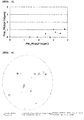
- FIG. 2 is an overlapped map ( FIG. 2(a) ) of surface LPDs before and after deposition of the polycrystalline silicon layer and a surface SEM/cross-sectional TEM image ( FIG. 2(b) ) of a defect detected at the same position.
- FIG. 2(a) it is often the case that the positions of the surface defects before deposition of the polycrystalline silicon layer coincide with the positions of the surface defects after deposition of the polycrystalline silicon layer.
- FIG. 2(b) shows an example of a result obtained by analyzing surface defects whose positions coincide with each other with the use of a surface SEM (Scanning Electron Microscope) and a cross-sectional TEM (Transmission Electron Microscope).
- the analysis using the cross-sectional TEM has revealed that the defect on the PW surface is a pit and the defect on the polycrystalline silicon layer surface is also a pit.
- FIG. 4 shows this result. As shown in the overlapped map of FIG. 4 , it has been found out that the defects detected at the same position before and after deposition of the polycrystalline silicon layer become voids 100% after bonding.
- this discovery is the discovery of an evaluation method which enables detecting only defects which cause voids of a bonded SOI wafer at high sensitivity.
- this evaluation method is incorporated in a substrate-to-be-bonded manufacturing process, only wafers having defects which cause voids can be selectively determined as defective products, and manufacturing yield loss of the substrates to be bonded (an excessive reduction in manufacturing yield) can be rationally avoided.
- a substrate-to-be-bonded quality determining standard is set to the number of surface defects of a polycrystalline silicon layer alone. At this rate, however, as shown in FIG. 4 , wafers having only defects which do not cause voids are also determined as defective products, and hence the substrate-to-be-bonded manufacturing yield is lowered more than necessity.
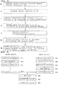
- FIG. 1 A more detailed description will now be given on the present invention with reference to a process flowchart of the method for evaluating surface defects of a substrate to be bonded according to the present invention shown in FIG. 1 .
- a mirror-polished silicon single crystal substrate (PW: Polished Wafer) is prepared (a step A).
- a general method for manufacturing a silicon single crystal substrate can be used for manufacture of the silicon single crystal substrate to be prepared and, specifically, a silicon single crystal substrate subjected to single-crystal pulling, cylindrical grinding, notch machining, slicing, chamfering, lapping, etching, double-side polishing, mirror edge polishing, final polishing, and the like can be used.
- a step B surface defects of the mirror-polished silicon single crystal substrate are inspected. It is preferable to inspect the surface defects on the silicon single crystal substrate surface subjected to final cleaning after the final polishing.
- coordinate data of all detected defects is acquired and recorded. The coordinate data can be acquired as a KLARF file when the defect detector is Surfscan SPX manufactured by KLA-Tencor Corporation.
- the standard can be set at this step, the pits are completely filled by subsequent deposition of a polycrystalline silicon layer or, even if the pits are not completely filled, they remain as such shallow pits that they are flattened by polishing at a later step, or defects to be remedied are also present.
- the polycrystalline silicon layer is deposited on the surface of the silicon single crystal substrate subjected to the defect inspection (a step C).
- the deposition of the polycrystalline silicon layer can be carried out in accordance with, e.g., a technology described in Patent Literature 2.
- a film thickness of the polycrystalline silicon layer is set to, e.g., 1 to 5 ⁇ m or preferably 2 to 3 ⁇ m while considering a later polishing stock removal.
- SC1 a mixed aqueous solution of NH 4 OH and H 2 O 2
- SC2 a mixed aqueous solution of HCl and H 2 O 2
- cleaning for a hydrophilic surface forming treatment such as ozonated water cleaning.
- the mirror edge polishing is performed to the silicon single crystal substrate having the polycrystalline silicon layer deposited thereon (a step D).
- the same mirror edge polishing as that performed at the step of manufacturing the mirror-polished silicon single crystal substrate is carried out to remove a polycrystalline silicon film grown on a wafer edge portion.
- a workpiece holder which is disposed to a polishing head and called a template is used.
- the template is a composite base material of a glass epoxy resin ring and a backing pad, and an inner peripheral wall of this glass epoxy resin ring is constantly in contact with a silicon single crystal substrate edge portion during polishing. That is, the mirror edge polishing is performed here to reduce dust emission from the edge portion or sliding friction against the ring inner peripheral wall.
- the surface of the polycrystalline silicon layer is polished (a step E).
- the same surface polishing as that performed at the step of manufacturing the mirror-polished silicon single crystal substrate is carried out to the polycrystalline silicon layer.
- Setting a polishing stock removal to 0.4 ⁇ m or more is preferable for an improvement in surface roughness. Furthermore, setting the polishing stock removal to 1 ⁇ m or less enables enhancing productivity.
- step F surface defects on the polished polycrystalline silicon layer are inspected.
- measurement using the same inspection tool and the same threshold value conditions as those of the step of inspecting the surface defects on the silicon single crystal substrate (the step B) is carried out to the polycrystalline silicon layer surface subjected to the final cleaning after the polishing. Coordinate data of all detected defects is acquired and recorded in the same manner as the step B.
- the coordinates of the defects detected at the step of inspecting the surface defects on the silicon single crystal substrate are compared with the coordinates of the surface defects detected at the step of inspecting the surface defects on the polycrystalline silicon layer (the step F), and quality of the silicon single crystal substrate having the polycrystalline silicon layer as the substrate to be bonded is determined on the basis of presence/absence of detects present at the same position (a step G).
- a distance between both defects is 500 ⁇ m or less, these defects can be determined as the same defect while taking a coordinate accuracy in the defect measurement into consideration.
- the substrate to be bonded having the defects determined to be present at the same position is regarded as a defective product, and any other substrate to be bonded can be regarded as a non-defective product. Additionally, the substrate to be bonded determined to be a non-defective product can be submitted to a bonding step. It is to be noted that when the polishing of the deposited polycrystalline silicon layer is finished, the silicon single crystal substrate can be called the substrate to be bonded.
- FIG. 5 shows a process flowchart of a conventional method for evaluating surface defects of a substrate to be bonded.
- steps H, J, K, and L are the same as the steps A, C, D, and E in the method for evaluating surface defects of a substrate to be bonded according to the present invention, a description thereof will be omitted to avoid overlap.
- the conventional method for evaluating surface defects of a substrate to be bonded has a step of inspecting surface defects on a mirror-polished silicon single crystal substrate (a step I), coordinates of detected defects do not have to be recorded. Further, the conventional method for evaluating surface defects of a substrate to be bonded has a step of inspecting surface defects on a polished polycrystalline silicon layer (a step M). In the conventional method, a standard for a quality determination of substrates to be bonded is provided to only the number of defects detected at this step.
- a void defect occurrence ratio of bonded SOI wafers increases when the standard for the number of defects is loosely set to enhance a manufacturing yield of the substrates to be bonded and, on the other hand, the manufacturing yield of the substrates to be bonded extremely decreases when the standard for the number of defects is rigorously set to reduce the void defect occurrence ratio of the bonded SOI wafers.
- the substrate to be bonded used in the method for evaluating surface defects on a substrate to be bonded according to the present invention is a base wafer for the bonded SOI wafer.
- the method for evaluating surface defects of a substrate to be bonded according to the present invention can be preferably applied to a manufacturing process of the bonded SOI wafer for advanced radio frequency devices.
- One hundred mirror-polished silicon single crystal substrates (diameter: 300 mm, crystal orientation: ⁇ 100>) were prepared.
- SurfScan SP2 of KLA-Tencor Corporation was used for an inspection of surface defects of these mirror-polished silicon single crystal substrates, and a detection threshold value of defect sizes was set to 250 nm. After the defect inspection, coordinates of detected defects were recorded. Then, a polycrystalline silicon layer having a film thickness of 3 ⁇ m was deposited on the surfaces of the silicon single crystal substrates subjected to the defect inspection, and SC1 and SC2 cleaning was carried out. Thereafter, the mirror edge polishing was performed to the silicon single crystal substrates each having the polycrystalline silicon layer deposited thereon.
- a polishing stock removal was set to 1 ⁇ m, the respective polycrystalline silicon layers were polished, and the SC1 and SC2 cleaning was carried out. Subsequently, the surfaces of the polished polycrystalline silicon layers were inspected under the same conditions as those described above by using SurfScan SP2, and coordinates of detected defects were recorded.
- each mirror-polished silicon single crystal substrate was compared and collated with the defect coordinates on the surface of each polished polycrystalline silicon layer. If a distance between both defects was 500 ⁇ m or less, the defects were regarded as defects present at the same position, and each evaluation target substrate-to-be-bonded having the defects present at the same position was determined as a defective product. A manufacturing yield of the substrates to be bonded at this moment was 97%. Additionally, each non-defective substrate to be bonded was subjected to a bonded SOI process as a base wafer to manufacture a bonded SOI wafer.
- Voids of each bonded SOI wafer were measured by scanning the entire wafer surface with the use of a bright-field optical microscope to take in images and comparing contrasts of the images to extract defects.
- a detection threshold value here was set to 10 ⁇ m.
- a void (defect) occurrence ratio here (a ratio of wafers having defects produced thereon among the manufactured bonded SOI wafers) was 2.0%.
- Table 1 shows the above-described results of Example. [Table 1] Standard Manufacturing yield [%] N Subject non-defective products to bonded SOI process Void occurrence ratio [%] Example No defects at same position 97 100 2.0 Comparative Example 1 ⁇ 3 96 100 7.2 Comparative Example 2 ⁇ 2 95 100 ⁇ 6.3 Comparative Example 3 ⁇ 1 93 100 3.2
- each non-defective substrate to be bonded was subjected to a bonded SOI process as a base wafer to manufacture a bonded SOI wafer.
- Voids of each bonded SOI wafer were measured by scanning the entire wafer surface with the use of a bright-field optical microscope to take in images and comparing contrasts of the images to extract defects.
- a detection threshold value here was set to 10 ⁇ m.
- a void occurrence ratio here was 7.2%.
- Table 1 shows the above-described results of Comparative Example 1.
- Comparative Example 2 the quality of each substrate to be bonded was determined in the same manner as Comparative Example 1 except that the standard for the number of defects on a surface of each polished polycrystalline silicon layer was set to two. A manufacturing yield of the substrates to be bonded here was 95%. Further, a void occurrence ratio was obtained in the same manner as Comparative Example 1, and then a result was 6.3%. Table 1 shows the above-described results of Comparative Example 2.
- Comparative Example 3 the quality of each substrate to be bonded was determined in the same manner as Comparative Example 1 except that the standard for the number of defects on a surface of each polished polycrystalline silicon layer was set to one. A manufacturing yield of the substrates to be bonded here was 93%. Further, a void occurrence ratio was obtained in the same manner as Comparative Example 1, and then a result was 3.2%. Table 1 shows the above-described results of Comparative Example 3.
- Example 2 the manufacturing yield of the substrates to be bonded was high, and the void occurrence ratio was low.
- the manufacturing yield was decreased by lowering the standard for the number of defects on each substrate to be bonded, but the void occurrence ratio was improved.
- Comparative Examples it was impossible to achieve both the high manufacturing yield of the substrates to be bonded and the low void occurrence ratio of the bonded SOI wafers. Thus, the effectiveness of the present invention was exhibited.
Landscapes
- General Health & Medical Sciences (AREA)
- Health & Medical Sciences (AREA)
- Life Sciences & Earth Sciences (AREA)
- Chemical & Material Sciences (AREA)
- Analytical Chemistry (AREA)
- Biochemistry (AREA)
- Physics & Mathematics (AREA)
- General Physics & Mathematics (AREA)
- Immunology (AREA)
- Pathology (AREA)
- Testing Or Measuring Of Semiconductors Or The Like (AREA)
- Investigating Materials By The Use Of Optical Means Adapted For Particular Applications (AREA)
- Mechanical Treatment Of Semiconductor (AREA)
Abstract
Description
- The present invention relates to a method for evaluating surface defects of substrate to be bonded.
- In a process of a bonded SOI wafer for advanced radio frequency devices, a silicon substrate having a polycrystalline silicon layer formed on a surface layer thereof is used as a base wafer in some situations. A bond wafer is additionally prepared in addition to this base wafer, both the wafers are bonded, and then the bond wafer is thinned to fabricate the bonded SOI wafer.
- Each of
Patent Literature 1 andPatent Literature 2 describes a method for manufacturing a bonded SOI wafer for radio frequency devices which uses a polycrystalline silicon layer as a carrier trap layer (which is also referred to as a trap-rich layer).FIG. 6 shows a process flow of the method for manufacturing a bonded SOI wafer described in each ofPatent Literature 1 andPatent Literature 2. They have a description that, as shown inFIG. 6 , in the method for manufacturing a bonded SOI wafer, a polycrystalline silicon layer is deposited on a base wafer (S23), and then a surface of the polycrystalline silicon layer is polished (S24), and the base wafer is bonded to the bond wafer (S31). Further,FIG. 7 shows an example of a cross section of the bonded SOI wafer manufactured in this manner. In thebonded SOI wafer 1 shown inFIG. 7 , apolycrystalline silicon layer 12, a buried oxide film layer (a BOX layer) 16, and anSOI layer 15 are formed on thebase wafer 11 in the mentioned order. -
- Patent Literature 1: Japanese Unexamined Patent Application Publication No.
2015-211074 - Patent Literature 2: Japanese Unexamined Patent Application Publication No.
2015-211061 - As a main failure item of bonded SOI wafers, there is a local unbonded region called a void defect, and its improvement has been demanded. In a manufacturing process of substrates to be bonded, it is known that each pit defect is one of causes of the void defects in the bonded SOI wafers. Thus, reducing a pit defect occurrence ratio and detecting pits at high sensitivity to prevent outflow to a bonding step are demanded.
- As a current method for detecting surface defects, there is a method for detecting surface detects by a defect inspection device using a light scattering method or differential interferometry as a detection principle. In a bonded wafer manufacturing process, providing size and quantity standards to surface defects detected by the defect inspection device prevents outflow of the surface defects to the bonding step. Although a void occurrence ratio at the bonding step can be reduced by lowering an upper limit of the quantity standard, a problem of degradation of a manufacturing yield of the substrates to be bonded also arises. At this time, if defects causing voids alone can be efficiently detected, unnecessary loss of the manufacturing yield of the substrates to be bonded can be avoided, and the void occurrence ratio after bonding can be also reduced. On the basis of such a background, in the substrate-to-be-bonded manufacturing step, a method for evaluating surfaces defects which detects only defects causing voids at high sensitivity has been demanded.
- In view of the above described problem, it is an object of the present invention to provide a method for evaluating surface defects of a substrate-to-be-bonded which enables rationally avoiding a reduction in manufacturing yield of a substrate to be bonded and reducing a void defect occurrence ratio after bonding by detecting surface defects of the substrate to be bonded, which can cause void defects in a bonded SOI wafer, at high sensitivity.
- To achieve the object, the present invention provides a method for evaluating surface defects of a substrate to be bonded, including the steps of:
- preparing a mirror-polished silicon single crystal substrate;
- inspecting surface defects on the mirror-polished silicon single crystal substrate;
- depositing a polycrystalline silicon layer on a surface of the silicon single crystal substrate subjected to the defect inspection;
- performing mirror edge polishing to the silicon single crystal substrate having the polycrystalline silicon layer deposited thereon;
- polishing a surface of the polycrystalline silicon layer;
- inspecting surface defects on the polished polycrystalline silicon layer; and
- comparing coordinates of defects detected at the step of inspecting the surface defects on the silicon single crystal substrate with counterparts detected at the step of inspecting the surface defects on the polycrystalline silicone layer and determining quality of the silicon single crystal substrate having the polycrystalline silicon layer as a substrate to be bonded on the basis of presence/absence of defects present at the same position.
- As described above, when the surface defects are inspected on both the surface of the mirror-polished silicon single crystal substrate and the surface of the polycrystalline silicon layer which has been polished after deposition of the polycrystalline silicon layer and only the substrate to be bonded having the surface defects at the same position is determined as a defective product, both rational avoidance of a reduction in manufacturing yield of the substrate-to-be-bonded and a reduction in void defect occurrence ratio of the bonded SOI wafer can be achieved.
- At this time, it is preferable that the substrate to be bonded is a base wafer for a bonded SOI wafer.
- As described above, when the substrate to be bonded is the base wafer for the bonded SOI wafer, the method for evaluating surface defects of a substrate to be bonded according to the present invention can be preferably applied to a process of manufacturing a bonded SOI wafer for advance radio frequency devices.
- According to the present invention, when surface defects are inspected on both the surface of the mirror-polished silicon single crystal substrate before depositing the polycrystalline silicon layer and the surface of the polycrystalline silicon layer polished after depositing the polycrystalline silicon layer and only the substrate to be bonded having the surface defects at the same position is determined as a defective product, both avoidance of manufacturing yield loss of the substrate to be bonded and a reduction in void defect occurrence ratio of the bonded SOI wafer can be achieved.
-
-
FIG. 1 is a process flowchart of a method for evaluating surface defects of a substrate to be bonded according to the present invention; -
FIG. 2 is an overlapped map (a) of surface LPDs (Light Point Defects) before and after deposition of a polycrystalline silicon layer and a surface SEM/cross-sectional TEM image (b) of defects detected at the same position; -
FIG. 3 is a graph showing a relationship between a pit depth of a mirror-polished silicon single crystal substrate (PW) surface and a pit depth of a polycrystalline silicon layer surface (after polishing); -
FIG. 4 is an overlapped map of surface LPDs before and after deposition of polycrystalline silicon and voids of a bonded SOI wafer; -
FIG. 5 is a process flowchart of a conventional method for evaluating surface defects of a substrate to be bonded; -
FIG. 6 is a process flowchart of a conventional method for manufacturing a bonded SOI wafer; and -
FIG. 7 is a cross-sectional view of a bonded SOI wafer. - As described above, in methods for evaluating surface defects of a substrate to be bonded, a method for evaluating surface defects of a substrate-to-be-bonded which enables avoiding loss of a manufacturing yield of the substrate to be bonded and reducing a void defect occurrence ratio of a bonded SOI wafer has been demanded.
- As a result of conducting keen examinations to achieve the object, the present inventors have discovered that the problem can be solved by inspecting surface defects on both a PW (Polished Wafer) surface before depositing a polycrystalline silicon layer and a polycrystalline silicon layer surface polished after depositing the polycrystalline silicon layer and determining only wafers having surface defects at the same position as defective products, thus bringing the present invention to completion.
- A detailed description will be given below on the present invention with reference to the drawings, but the present invention is not restricted thereto.
- First, a relationship between defects on the PW surface and defects on the polished polycrystalline silicon layer surface was examined. Usually, in the substrate to be bonded, the polycrystalline silicon layer is deposited with a thickness of 2 to 3 µm, and then polished by 0.4 to 1 µm to reduce surface roughness. The PW surface before deposition of the polycrystalline silicon layer and the polycrystalline silicon layer surface after deposition of the polycrystalline silicon layer and after polishing were measured with a detection threshold value of 250 nm by using a surface defect inspection machine such as SurfScan SP2 manufactured by KLA-TENCOR CORPORATION. Defect coordinates of both the surfaces were compared and collated, and then presence of defects at the same position was discovered.
- The defects present at the same position were analyzed in detail.
FIG. 2 is an overlapped map (FIG. 2(a) ) of surface LPDs before and after deposition of the polycrystalline silicon layer and a surface SEM/cross-sectional TEM image (FIG. 2(b) ) of a defect detected at the same position. As shown inFIG. 2(a) , it is often the case that the positions of the surface defects before deposition of the polycrystalline silicon layer coincide with the positions of the surface defects after deposition of the polycrystalline silicon layer.FIG. 2(b) shows an example of a result obtained by analyzing surface defects whose positions coincide with each other with the use of a surface SEM (Scanning Electron Microscope) and a cross-sectional TEM (Transmission Electron Microscope). The analysis using the cross-sectional TEM has revealed that the defect on the PW surface is a pit and the defect on the polycrystalline silicon layer surface is also a pit. - Conducting further evaluation and analysis has revealed that a pit depth of the PW surface and a pit depth of the polished polycrystalline silicon layer surface have a relationship shown in
FIG. 3 . - On the basis of the result shown in
FIG. 3 , it has been found out that, when the PW surface has a pit whose depth is 3 µm or more, the pit cannot be filled in the polycrystalline silicon layer, and the pit also remains on the polycrystalline silicon layer surface even if polishing is performed. On the contrary, the result suggests that, when the pit depth of the PW surface is less than 3 µm, the pit can be filled in the polycrystalline silicon layer, or it is completely flattened by polishing even though it is not perfectly filled. - Furthermore, a bonded SOI wafer was fabricated by using this substrate to be bonded, an entire wafer surface was scanned by a bright-field optical microscope to take in images, and void defects were extracted by comparing contrasts of the images. Then, coordinates of the void defects were superimposed on the overlapped map.
FIG. 4 shows this result. As shown in the overlapped map ofFIG. 4 , it has been found out that the defects detected at the same position before and after deposition of the polycrystalline silicon layer become voids 100% after bonding. - Changing the viewpoint, it can be said that this discovery is the discovery of an evaluation method which enables detecting only defects which cause voids of a bonded SOI wafer at high sensitivity. When this evaluation method is incorporated in a substrate-to-be-bonded manufacturing process, only wafers having defects which cause voids can be selectively determined as defective products, and manufacturing yield loss of the substrates to be bonded (an excessive reduction in manufacturing yield) can be rationally avoided.
- In a conventional bonded SOI wafer manufacturing process, a substrate-to-be-bonded quality determining standard is set to the number of surface defects of a polycrystalline silicon layer alone. At this rate, however, as shown in
FIG. 4 , wafers having only defects which do not cause voids are also determined as defective products, and hence the substrate-to-be-bonded manufacturing yield is lowered more than necessity. - A more detailed description will now be given on the present invention with reference to a process flowchart of the method for evaluating surface defects of a substrate to be bonded according to the present invention shown in
FIG. 1 . - First, a mirror-polished silicon single crystal substrate (PW: Polished Wafer) is prepared (a step A). A general method for manufacturing a silicon single crystal substrate can be used for manufacture of the silicon single crystal substrate to be prepared and, specifically, a silicon single crystal substrate subjected to single-crystal pulling, cylindrical grinding, notch machining, slicing, chamfering, lapping, etching, double-side polishing, mirror edge polishing, final polishing, and the like can be used.
- Then, surface defects of the mirror-polished silicon single crystal substrate are inspected (a step B). It is preferable to inspect the surface defects on the silicon single crystal substrate surface subjected to final cleaning after the final polishing. As a surface defect inspection tool, Surfscan SPX (X=1 to 3) manufactured by KLA-Tencor Corporation can be used, and scattered lights in a dark field are detected as LPDs. It is preferable to set a detection threshold value to detect problematic pits to 250 nm or more. At this time, coordinate data of all detected defects is acquired and recorded. The coordinate data can be acquired as a KLARF file when the defect detector is Surfscan SPX manufactured by KLA-Tencor Corporation. Although the standard can be set at this step, the pits are completely filled by subsequent deposition of a polycrystalline silicon layer or, even if the pits are not completely filled, they remain as such shallow pits that they are flattened by polishing at a later step, or defects to be remedied are also present. Thus, in view of a manufacturing yield of the mirror-polished silicon single crystal substrate, it is preferable to set no standard at this step or to configure a very rough setting.
- Then, the polycrystalline silicon layer is deposited on the surface of the silicon single crystal substrate subjected to the defect inspection (a step C). The deposition of the polycrystalline silicon layer can be carried out in accordance with, e.g., a technology described in
Patent Literature 2. A film thickness of the polycrystalline silicon layer is set to, e.g., 1 to 5 µm or preferably 2 to 3 µm while considering a later polishing stock removal. Further, after forming the polycrystalline silicon layer, it is preferable to perform cleaning using SC1 (a mixed aqueous solution of NH4OH and H2O2) and SC2 (a mixed aqueous solution of HCl and H2O2) or cleaning for a hydrophilic surface forming treatment such as ozonated water cleaning. When the hydrophilic surface is formed, adhesion of slurry burn can be avoided at a subsequent mirror edge polishing step. - Then, the mirror edge polishing is performed to the silicon single crystal substrate having the polycrystalline silicon layer deposited thereon (a step D). As this mirror edge polishing, the same mirror edge polishing as that performed at the step of manufacturing the mirror-polished silicon single crystal substrate is carried out to remove a polycrystalline silicon film grown on a wafer edge portion. At a subsequent polishing step, a workpiece holder which is disposed to a polishing head and called a template is used. The template is a composite base material of a glass epoxy resin ring and a backing pad, and an inner peripheral wall of this glass epoxy resin ring is constantly in contact with a silicon single crystal substrate edge portion during polishing. That is, the mirror edge polishing is performed here to reduce dust emission from the edge portion or sliding friction against the ring inner peripheral wall.
- Then, the surface of the polycrystalline silicon layer is polished (a step E). At this step, the same surface polishing as that performed at the step of manufacturing the mirror-polished silicon single crystal substrate is carried out to the polycrystalline silicon layer. Setting a polishing stock removal to 0.4 µm or more is preferable for an improvement in surface roughness. Furthermore, setting the polishing stock removal to 1 µm or less enables enhancing productivity.
- Subsequently, surface defects on the polished polycrystalline silicon layer are inspected (a step F). At this step, measurement using the same inspection tool and the same threshold value conditions as those of the step of inspecting the surface defects on the silicon single crystal substrate (the step B) is carried out to the polycrystalline silicon layer surface subjected to the final cleaning after the polishing. Coordinate data of all detected defects is acquired and recorded in the same manner as the step B.
- Moreover, the coordinates of the defects detected at the step of inspecting the surface defects on the silicon single crystal substrate (the step B) are compared with the coordinates of the surface defects detected at the step of inspecting the surface defects on the polycrystalline silicon layer (the step F), and quality of the silicon single crystal substrate having the polycrystalline silicon layer as the substrate to be bonded is determined on the basis of presence/absence of detects present at the same position (a step G). Here, when a distance between both defects is 500 µm or less, these defects can be determined as the same defect while taking a coordinate accuracy in the defect measurement into consideration. Only the substrate to be bonded having the defects determined to be present at the same position is regarded as a defective product, and any other substrate to be bonded can be regarded as a non-defective product. Additionally, the substrate to be bonded determined to be a non-defective product can be submitted to a bonding step. It is to be noted that when the polishing of the deposited polycrystalline silicon layer is finished, the silicon single crystal substrate can be called the substrate to be bonded.
- For comparison,
FIG. 5 shows a process flowchart of a conventional method for evaluating surface defects of a substrate to be bonded. InFIG. 5 , since steps H, J, K, and L are the same as the steps A, C, D, and E in the method for evaluating surface defects of a substrate to be bonded according to the present invention, a description thereof will be omitted to avoid overlap. - Although the conventional method for evaluating surface defects of a substrate to be bonded has a step of inspecting surface defects on a mirror-polished silicon single crystal substrate (a step I), coordinates of detected defects do not have to be recorded. Further, the conventional method for evaluating surface defects of a substrate to be bonded has a step of inspecting surface defects on a polished polycrystalline silicon layer (a step M). In the conventional method, a standard for a quality determination of substrates to be bonded is provided to only the number of defects detected at this step. Thus, a void defect occurrence ratio of bonded SOI wafers increases when the standard for the number of defects is loosely set to enhance a manufacturing yield of the substrates to be bonded and, on the other hand, the manufacturing yield of the substrates to be bonded extremely decreases when the standard for the number of defects is rigorously set to reduce the void defect occurrence ratio of the bonded SOI wafers.
- In the method for evaluating surface defects of a substrate to be bonded according to the present invention, surface defects are inspected on both the surface of the mirror-polished silicon single crystal substrate before deposition of the polycrystalline silicon layer and the surface of the polycrystalline silicon layer polished after deposition of the polycrystalline silicon layer, and each substrate to be bonded having the surface defects at the same position alone are determined as a defective product, whereby both rational avoidance of a reduction in manufacturing yield of the substrates to be bonded and a decrease in void defect occurrence ratio of the bonded SOI wafers can be achieved.
- Furthermore, it is preferable for the substrate to be bonded used in the method for evaluating surface defects on a substrate to be bonded according to the present invention to be a base wafer for the bonded SOI wafer. When the substrate to be bonded is the base wafer for the bonded SOI wafer, the method for evaluating surface defects of a substrate to be bonded according to the present invention can be preferably applied to a manufacturing process of the bonded SOI wafer for advanced radio frequency devices.
- The present invention will now be more specifically described with reference to an example and comparative examples, but the present invention is not restricted thereto.
- One hundred mirror-polished silicon single crystal substrates (diameter: 300 mm, crystal orientation: <100>) were prepared. SurfScan SP2 of KLA-Tencor Corporation was used for an inspection of surface defects of these mirror-polished silicon single crystal substrates, and a detection threshold value of defect sizes was set to 250 nm. After the defect inspection, coordinates of detected defects were recorded. Then, a polycrystalline silicon layer having a film thickness of 3 µm was deposited on the surfaces of the silicon single crystal substrates subjected to the defect inspection, and SC1 and SC2 cleaning was carried out. Thereafter, the mirror edge polishing was performed to the silicon single crystal substrates each having the polycrystalline silicon layer deposited thereon. Then, a polishing stock removal was set to 1 µm, the respective polycrystalline silicon layers were polished, and the SC1 and SC2 cleaning was carried out. Subsequently, the surfaces of the polished polycrystalline silicon layers were inspected under the same conditions as those described above by using SurfScan SP2, and coordinates of detected defects were recorded.
- Moreover, the defect coordinates on the surface of each mirror-polished silicon single crystal substrate were compared and collated with the defect coordinates on the surface of each polished polycrystalline silicon layer. If a distance between both defects was 500 µm or less, the defects were regarded as defects present at the same position, and each evaluation target substrate-to-be-bonded having the defects present at the same position was determined as a defective product. A manufacturing yield of the substrates to be bonded at this moment was 97%. Additionally, each non-defective substrate to be bonded was subjected to a bonded SOI process as a base wafer to manufacture a bonded SOI wafer. Voids of each bonded SOI wafer were measured by scanning the entire wafer surface with the use of a bright-field optical microscope to take in images and comparing contrasts of the images to extract defects. A detection threshold value here was set to 10 µm. A void (defect) occurrence ratio here (a ratio of wafers having defects produced thereon among the manufactured bonded SOI wafers) was 2.0%. Table 1 shows the above-described results of Example.
[Table 1] Standard Manufacturing yield [%] N Subject non-defective products to bonded SOI process Void occurrence ratio [%] Example No defects at same position 97 100 2.0 Comparative Example 1 ≤3 96 100 7.2 Comparative Example 2 ≤2 95 100 → 6.3 Comparative Example 3 ≤1 93 100 3.2 - First, 100 mirror-polished silicon single crystal substrates were prepared. SurfScan SP2 of KLA-Tencor Corporation was used for an inspection of surface defects of these mirror-polished silicon single crystal substrates, and a detection threshold value of defect sizes was set to 250 nm. Here, all substrates were determined as non-defective products without providing standards. Subsequently, a polycrystalline silicon layer having a film thickness of 3 µm was deposited on the surfaces of the silicon single crystal substrates subjected to the defect inspection, and SC1 and SC2 cleaning was carried out. Thereafter, the mirror edge polishing was performed to the silicon single crystal substrates each having the polycrystalline silicon deposited thereon. Then, a polishing stock removal was set to 1 µm, the respective polycrystalline silicon layers were polished, and the SC1 and SC2 cleaning was carried out. Subsequently, the surfaces of the polished polycrystalline silicon layers were inspected under the same conditions as those described above by using SurfScan SP2, and the number of defects were thereby obtained. In Comparative Example 1, the standard for the number of defects was set to three. A manufacturing yield of the substrates to be bonded at this moment was 96%.
- Additionally, each non-defective substrate to be bonded was subjected to a bonded SOI process as a base wafer to manufacture a bonded SOI wafer. Voids of each bonded SOI wafer were measured by scanning the entire wafer surface with the use of a bright-field optical microscope to take in images and comparing contrasts of the images to extract defects. A detection threshold value here was set to 10 µm. A void occurrence ratio here was 7.2%. Table 1 shows the above-described results of Comparative Example 1.
- In Comparative Example 2, the quality of each substrate to be bonded was determined in the same manner as Comparative Example 1 except that the standard for the number of defects on a surface of each polished polycrystalline silicon layer was set to two. A manufacturing yield of the substrates to be bonded here was 95%. Further, a void occurrence ratio was obtained in the same manner as Comparative Example 1, and then a result was 6.3%. Table 1 shows the above-described results of Comparative Example 2.
- In Comparative Example 3, the quality of each substrate to be bonded was determined in the same manner as Comparative Example 1 except that the standard for the number of defects on a surface of each polished polycrystalline silicon layer was set to one. A manufacturing yield of the substrates to be bonded here was 93%. Further, a void occurrence ratio was obtained in the same manner as Comparative Example 1, and then a result was 3.2%. Table 1 shows the above-described results of Comparative Example 3.
- As described above, in Example, the manufacturing yield of the substrates to be bonded was high, and the void occurrence ratio was low. On the other hand, in each of Comparative Examples 1 to 3, the manufacturing yield was decreased by lowering the standard for the number of defects on each substrate to be bonded, but the void occurrence ratio was improved. However, in Comparative Examples, it was impossible to achieve both the high manufacturing yield of the substrates to be bonded and the low void occurrence ratio of the bonded SOI wafers. Thus, the effectiveness of the present invention was exhibited.
- It is to be noted that the present invention is not restricted to the foregoing embodiment. The foregoing embodiment is an illustrative example, and any example which has substantially the same structure and exerts the same functions and effects as the technical concept described in claims of the present invention is included in the technical scope of the present invention.
Claims (2)
- A method for evaluating surface defects of a substrate to be bonded, comprising the steps of:preparing a mirror-polished silicon single crystal substrate;inspecting surface defects on the mirror-polished silicon single crystal substrate;depositing a polycrystalline silicon layer on a surface of the silicon single crystal substrate subjected to the defect inspection;performing mirror edge polishing to the silicon single crystal substrate having the polycrystalline silicon layer deposited thereon;polishing a surface of the polycrystalline silicon layer;inspecting surface defects on the polished polycrystalline silicon layer; andcomparing coordinates of defects detected at the step of inspecting the surface defects on the silicon single crystal substrate with counterparts detected at the step of inspecting the surface defects on the polycrystalline silicone layer and determining quality of the silicon single crystal substrate having the polycrystalline silicon layer as a substrate to be bonded on the basis of presence/absence of defects present at the same position.
- The method for evaluating surface defects of a substrate to be bonded according to claim 1,
wherein the substrate to be bonded is a base wafer for a bonded SOI wafer.
Applications Claiming Priority (2)
| Application Number | Priority Date | Filing Date | Title |
|---|---|---|---|
| JP2016175044A JP6614076B2 (en) | 2016-09-07 | 2016-09-07 | Method for evaluating surface defects of substrates for bonding |
| PCT/JP2017/027102 WO2018047501A1 (en) | 2016-09-07 | 2017-07-26 | Bonding substrate surface defect evaluation method |
Publications (3)
| Publication Number | Publication Date |
|---|---|
| EP3511976A1 true EP3511976A1 (en) | 2019-07-17 |
| EP3511976A4 EP3511976A4 (en) | 2020-04-22 |
| EP3511976B1 EP3511976B1 (en) | 2023-01-04 |
Family
ID=61561765
Family Applications (1)
| Application Number | Title | Priority Date | Filing Date |
|---|---|---|---|
| EP17848446.5A Active EP3511976B1 (en) | 2016-09-07 | 2017-07-26 | Bonding substrate surface defect evaluation method |
Country Status (8)
| Country | Link |
|---|---|
| US (1) | US10707140B2 (en) |
| EP (1) | EP3511976B1 (en) |
| JP (1) | JP6614076B2 (en) |
| KR (1) | KR102327328B1 (en) |
| CN (1) | CN109643670B (en) |
| SG (1) | SG11201901686QA (en) |
| TW (1) | TWI722225B (en) |
| WO (1) | WO2018047501A1 (en) |
Families Citing this family (6)
| Publication number | Priority date | Publication date | Assignee | Title |
|---|---|---|---|---|
| JP7172951B2 (en) * | 2019-10-31 | 2022-11-16 | 信越半導体株式会社 | Semiconductor wafer evaluation method, semiconductor wafer sorting method, and device manufacturing method |
| EP4160660A4 (en) * | 2020-06-01 | 2024-03-20 | Shin-Etsu Handotai Co., Ltd. | METHOD FOR EVALUATING AN EXTERNAL PERIPHERAL DEFORMATION OF A WAFER |
| US12176202B2 (en) * | 2020-10-08 | 2024-12-24 | Okmetic Oy | Manufacture method of a high-resistivity silicon handle wafer for a hybrid substrate structure |
| CN112951735B (en) * | 2021-01-28 | 2022-11-08 | 微龛(广州)半导体有限公司 | Wafer bonding quality detection method and system |
| CN114034535B (en) * | 2021-11-09 | 2024-04-30 | 四川华能康定水电有限责任公司 | On-site coating quality assessment auxiliary method and system |
| CN114994058A (en) * | 2022-06-09 | 2022-09-02 | 杭州利珀科技有限公司 | Silicon chip stacking detection system and method |
Family Cites Families (19)
| Publication number | Priority date | Publication date | Assignee | Title |
|---|---|---|---|---|
| JPH06252230A (en) * | 1993-02-24 | 1994-09-09 | Hitachi Ltd | Method and apparatus for inspection of defect |
| JP3633062B2 (en) * | 1994-12-22 | 2005-03-30 | 株式会社デンソー | Polishing method and polishing apparatus |
| JP3664134B2 (en) * | 1999-10-14 | 2005-06-22 | 三菱住友シリコン株式会社 | Inspection method of semiconductor wafer surface |
| JP4104396B2 (en) * | 2002-07-31 | 2008-06-18 | 株式会社ニデック | Appearance inspection device |
| JP4507157B2 (en) * | 2003-06-17 | 2010-07-21 | 信越半導体株式会社 | Wafer manufacturing process management method |
| JP2005166846A (en) * | 2003-12-01 | 2005-06-23 | Sumitomo Mitsubishi Silicon Corp | Hf defect measuring method for soi substrate |
| JP4789630B2 (en) * | 2006-01-19 | 2011-10-12 | 株式会社東京精密 | Semiconductor manufacturing apparatus, semiconductor appearance inspection apparatus, and appearance inspection method |
| KR20080073584A (en) * | 2007-02-06 | 2008-08-11 | 주식회사 하이닉스반도체 | Surface inspection method of silicon wafer |
| JP5372365B2 (en) * | 2007-12-25 | 2013-12-18 | 株式会社日立ハイテクノロジーズ | Inspection apparatus and inspection method |
| JP2010021242A (en) * | 2008-07-09 | 2010-01-28 | Sumco Corp | Method of detecting defect in laminating wafer |
| US8664092B2 (en) * | 2009-06-26 | 2014-03-04 | Sumco Corporation | Method for cleaning silicon wafer, and method for producing epitaxial wafer using the cleaning method |
| TWI498954B (en) * | 2009-08-21 | 2015-09-01 | 勝高股份有限公司 | Method for manufacturing epitaxial wafer |
| US9224660B2 (en) * | 2013-08-30 | 2015-12-29 | Kla-Tencor Corp. | Tuning wafer inspection recipes using precise defect locations |
| JP6100200B2 (en) | 2014-04-24 | 2017-03-22 | 信越半導体株式会社 | Manufacturing method of bonded SOI wafer |
| JP6118757B2 (en) | 2014-04-24 | 2017-04-19 | 信越半導体株式会社 | Manufacturing method of bonded SOI wafer |
| CN104201131B (en) * | 2014-09-02 | 2017-03-08 | 上海华力微电子有限公司 | The method that assessment polysilicon gate oxide layer lacks defect |
| CN104217973B (en) * | 2014-09-02 | 2017-03-08 | 上海华力微电子有限公司 | The method of detection polysilicon gate oxide layer disappearance |
| JP6045542B2 (en) * | 2014-09-11 | 2016-12-14 | 信越半導体株式会社 | Semiconductor wafer processing method, bonded wafer manufacturing method, and epitaxial wafer manufacturing method |
| JP6179530B2 (en) * | 2015-01-23 | 2017-08-16 | 信越半導体株式会社 | Manufacturing method of bonded SOI wafer |
-
2016
- 2016-09-07 JP JP2016175044A patent/JP6614076B2/en active Active
-
2017
- 2017-07-26 KR KR1020197006354A patent/KR102327328B1/en active Active
- 2017-07-26 WO PCT/JP2017/027102 patent/WO2018047501A1/en not_active Ceased
- 2017-07-26 CN CN201780051581.3A patent/CN109643670B/en active Active
- 2017-07-26 US US16/327,482 patent/US10707140B2/en active Active
- 2017-07-26 SG SG11201901686QA patent/SG11201901686QA/en unknown
- 2017-07-26 EP EP17848446.5A patent/EP3511976B1/en active Active
- 2017-07-31 TW TW106125676A patent/TWI722225B/en active
Also Published As
| Publication number | Publication date |
|---|---|
| EP3511976A4 (en) | 2020-04-22 |
| CN109643670A (en) | 2019-04-16 |
| TWI722225B (en) | 2021-03-21 |
| JP6614076B2 (en) | 2019-12-04 |
| SG11201901686QA (en) | 2019-03-28 |
| WO2018047501A1 (en) | 2018-03-15 |
| KR20190043546A (en) | 2019-04-26 |
| KR102327328B1 (en) | 2021-11-17 |
| EP3511976B1 (en) | 2023-01-04 |
| US20190181059A1 (en) | 2019-06-13 |
| TW201820498A (en) | 2018-06-01 |
| US10707140B2 (en) | 2020-07-07 |
| CN109643670B (en) | 2022-10-11 |
| JP2018041844A (en) | 2018-03-15 |
Similar Documents
| Publication | Publication Date | Title |
|---|---|---|
| EP3511976B1 (en) | Bonding substrate surface defect evaluation method | |
| CN104428882B (en) | Evaluation method and production method for semiconductor wafers | |
| JP6066729B2 (en) | Method for reducing width of non-bonded region in SOI structure, wafer manufactured by the method, and SOI structure | |
| US8772177B2 (en) | Semiconductor wafer and method of producing the same | |
| KR102444720B1 (en) | A method for mirror-chamfering a wafer, a method for manufacturing a wafer, and a wafer | |
| CN108140593A (en) | Judgment method of defect area | |
| CN109690746B (en) | Method for evaluating silicon wafer, method for evaluating silicon wafer manufacturing process, method for manufacturing silicon wafer, and silicon wafer | |
| TWI400743B (en) | Silicon wafer and its manufacturing method | |
| JP5472073B2 (en) | Semiconductor wafer and manufacturing method thereof | |
| US10559508B2 (en) | Method for manufacturing SiC substrate | |
| JP2013520838A5 (en) | ||
| TWI907218B (en) | Methods, apparatus, treatment methods, and products for detecting edge defects in silicon wafers. | |
| US6234873B1 (en) | Semiconductor mirror-polished surface wafers and method for manufacturing the same | |
| JP2025166173A (en) | Systems and methods for processing semiconductor wafers using front-end processed wafer shape metrics | |
| JP2019067952A (en) | Evaluating method of semiconductor wafer and manufacturing method of semiconductor wafer using the method | |
| JP4420023B2 (en) | Semiconductor wafer measurement method, manufacturing process management method, and semiconductor wafer manufacturing method | |
| JP2018182160A (en) | Evaluation method of semiconductor wafer and control method of semiconductor wafer manufacturing process | |
| JP2006108151A (en) | Method of manufacturing silicon epitaxial wafer | |
| JP2003177100A (en) | Quality evaluation method of mirror-finished and chamfered wafer | |
| US11211285B2 (en) | Method of producing bonded wafer and bonded wafer | |
| JP2019054132A (en) | Semiconductor wafer evaluation method | |
| US20170040285A1 (en) | Wafer planarization method | |
| JP2000243699A (en) | Semiconductor wafer manufacturing method and semiconductor device manufacturing method | |
| TW202516066A (en) | Method for forming silicon carbide substrate with optimized surface layer | |
| TW202614261A (en) | Systems and methods for wafer lift pin mark detection and uantitative analysis |
Legal Events
| Date | Code | Title | Description |
|---|---|---|---|
| STAA | Information on the status of an ep patent application or granted ep patent |
Free format text: STATUS: THE INTERNATIONAL PUBLICATION HAS BEEN MADE |
|
| PUAI | Public reference made under article 153(3) epc to a published international application that has entered the european phase |
Free format text: ORIGINAL CODE: 0009012 |
|
| STAA | Information on the status of an ep patent application or granted ep patent |
Free format text: STATUS: REQUEST FOR EXAMINATION WAS MADE |
|
| 17P | Request for examination filed |
Effective date: 20190225 |
|
| AK | Designated contracting states |
Kind code of ref document: A1 Designated state(s): AL AT BE BG CH CY CZ DE DK EE ES FI FR GB GR HR HU IE IS IT LI LT LU LV MC MK MT NL NO PL PT RO RS SE SI SK SM TR |
|
| AX | Request for extension of the european patent |
Extension state: BA ME |
|
| DAV | Request for validation of the european patent (deleted) | ||
| DAX | Request for extension of the european patent (deleted) | ||
| A4 | Supplementary search report drawn up and despatched |
Effective date: 20200324 |
|
| RIC1 | Information provided on ipc code assigned before grant |
Ipc: G01N 21/956 20060101ALI20200318BHEP Ipc: H01L 21/762 20060101ALI20200318BHEP Ipc: H01L 21/66 20060101AFI20200318BHEP |
|
| GRAP | Despatch of communication of intention to grant a patent |
Free format text: ORIGINAL CODE: EPIDOSNIGR1 |
|
| STAA | Information on the status of an ep patent application or granted ep patent |
Free format text: STATUS: GRANT OF PATENT IS INTENDED |
|
| INTG | Intention to grant announced |
Effective date: 20220818 |
|
| GRAS | Grant fee paid |
Free format text: ORIGINAL CODE: EPIDOSNIGR3 |
|
| GRAA | (expected) grant |
Free format text: ORIGINAL CODE: 0009210 |
|
| STAA | Information on the status of an ep patent application or granted ep patent |
Free format text: STATUS: THE PATENT HAS BEEN GRANTED |
|
| AK | Designated contracting states |
Kind code of ref document: B1 Designated state(s): AL AT BE BG CH CY CZ DE DK EE ES FI FR GB GR HR HU IE IS IT LI LT LU LV MC MK MT NL NO PL PT RO RS SE SI SK SM TR |
|
| REG | Reference to a national code |
Ref country code: GB Ref legal event code: FG4D |
|
| REG | Reference to a national code |
Ref country code: CH Ref legal event code: EP |
|
| REG | Reference to a national code |
Ref country code: AT Ref legal event code: REF Ref document number: 1542546 Country of ref document: AT Kind code of ref document: T Effective date: 20230115 |
|
| REG | Reference to a national code |
Ref country code: DE Ref legal event code: R096 Ref document number: 602017065280 Country of ref document: DE |
|
| REG | Reference to a national code |
Ref country code: IE Ref legal event code: FG4D |
|
| REG | Reference to a national code |
Ref country code: LT Ref legal event code: MG9D |
|
| REG | Reference to a national code |
Ref country code: NL Ref legal event code: MP Effective date: 20230104 |
|
| REG | Reference to a national code |
Ref country code: AT Ref legal event code: MK05 Ref document number: 1542546 Country of ref document: AT Kind code of ref document: T Effective date: 20230104 |
|
| PG25 | Lapsed in a contracting state [announced via postgrant information from national office to epo] |
Ref country code: NL Free format text: LAPSE BECAUSE OF FAILURE TO SUBMIT A TRANSLATION OF THE DESCRIPTION OR TO PAY THE FEE WITHIN THE PRESCRIBED TIME-LIMIT Effective date: 20230104 |
|
| PG25 | Lapsed in a contracting state [announced via postgrant information from national office to epo] |
Ref country code: RS Free format text: LAPSE BECAUSE OF FAILURE TO SUBMIT A TRANSLATION OF THE DESCRIPTION OR TO PAY THE FEE WITHIN THE PRESCRIBED TIME-LIMIT Effective date: 20230104 Ref country code: PT Free format text: LAPSE BECAUSE OF FAILURE TO SUBMIT A TRANSLATION OF THE DESCRIPTION OR TO PAY THE FEE WITHIN THE PRESCRIBED TIME-LIMIT Effective date: 20230504 Ref country code: NO Free format text: LAPSE BECAUSE OF FAILURE TO SUBMIT A TRANSLATION OF THE DESCRIPTION OR TO PAY THE FEE WITHIN THE PRESCRIBED TIME-LIMIT Effective date: 20230404 Ref country code: LV Free format text: LAPSE BECAUSE OF FAILURE TO SUBMIT A TRANSLATION OF THE DESCRIPTION OR TO PAY THE FEE WITHIN THE PRESCRIBED TIME-LIMIT Effective date: 20230104 Ref country code: LT Free format text: LAPSE BECAUSE OF FAILURE TO SUBMIT A TRANSLATION OF THE DESCRIPTION OR TO PAY THE FEE WITHIN THE PRESCRIBED TIME-LIMIT Effective date: 20230104 Ref country code: HR Free format text: LAPSE BECAUSE OF FAILURE TO SUBMIT A TRANSLATION OF THE DESCRIPTION OR TO PAY THE FEE WITHIN THE PRESCRIBED TIME-LIMIT Effective date: 20230104 Ref country code: ES Free format text: LAPSE BECAUSE OF FAILURE TO SUBMIT A TRANSLATION OF THE DESCRIPTION OR TO PAY THE FEE WITHIN THE PRESCRIBED TIME-LIMIT Effective date: 20230104 Ref country code: AT Free format text: LAPSE BECAUSE OF FAILURE TO SUBMIT A TRANSLATION OF THE DESCRIPTION OR TO PAY THE FEE WITHIN THE PRESCRIBED TIME-LIMIT Effective date: 20230104 |
|
| PG25 | Lapsed in a contracting state [announced via postgrant information from national office to epo] |
Ref country code: SE Free format text: LAPSE BECAUSE OF FAILURE TO SUBMIT A TRANSLATION OF THE DESCRIPTION OR TO PAY THE FEE WITHIN THE PRESCRIBED TIME-LIMIT Effective date: 20230104 Ref country code: PL Free format text: LAPSE BECAUSE OF FAILURE TO SUBMIT A TRANSLATION OF THE DESCRIPTION OR TO PAY THE FEE WITHIN THE PRESCRIBED TIME-LIMIT Effective date: 20230104 Ref country code: IS Free format text: LAPSE BECAUSE OF FAILURE TO SUBMIT A TRANSLATION OF THE DESCRIPTION OR TO PAY THE FEE WITHIN THE PRESCRIBED TIME-LIMIT Effective date: 20230504 Ref country code: GR Free format text: LAPSE BECAUSE OF FAILURE TO SUBMIT A TRANSLATION OF THE DESCRIPTION OR TO PAY THE FEE WITHIN THE PRESCRIBED TIME-LIMIT Effective date: 20230405 Ref country code: FI Free format text: LAPSE BECAUSE OF FAILURE TO SUBMIT A TRANSLATION OF THE DESCRIPTION OR TO PAY THE FEE WITHIN THE PRESCRIBED TIME-LIMIT Effective date: 20230104 |
|
| REG | Reference to a national code |
Ref country code: DE Ref legal event code: R097 Ref document number: 602017065280 Country of ref document: DE |
|
| PG25 | Lapsed in a contracting state [announced via postgrant information from national office to epo] |
Ref country code: SM Free format text: LAPSE BECAUSE OF FAILURE TO SUBMIT A TRANSLATION OF THE DESCRIPTION OR TO PAY THE FEE WITHIN THE PRESCRIBED TIME-LIMIT Effective date: 20230104 Ref country code: RO Free format text: LAPSE BECAUSE OF FAILURE TO SUBMIT A TRANSLATION OF THE DESCRIPTION OR TO PAY THE FEE WITHIN THE PRESCRIBED TIME-LIMIT Effective date: 20230104 Ref country code: EE Free format text: LAPSE BECAUSE OF FAILURE TO SUBMIT A TRANSLATION OF THE DESCRIPTION OR TO PAY THE FEE WITHIN THE PRESCRIBED TIME-LIMIT Effective date: 20230104 Ref country code: DK Free format text: LAPSE BECAUSE OF FAILURE TO SUBMIT A TRANSLATION OF THE DESCRIPTION OR TO PAY THE FEE WITHIN THE PRESCRIBED TIME-LIMIT Effective date: 20230104 Ref country code: CZ Free format text: LAPSE BECAUSE OF FAILURE TO SUBMIT A TRANSLATION OF THE DESCRIPTION OR TO PAY THE FEE WITHIN THE PRESCRIBED TIME-LIMIT Effective date: 20230104 |
|
| PLBE | No opposition filed within time limit |
Free format text: ORIGINAL CODE: 0009261 |
|
| STAA | Information on the status of an ep patent application or granted ep patent |
Free format text: STATUS: NO OPPOSITION FILED WITHIN TIME LIMIT |
|
| PG25 | Lapsed in a contracting state [announced via postgrant information from national office to epo] |
Ref country code: SK Free format text: LAPSE BECAUSE OF FAILURE TO SUBMIT A TRANSLATION OF THE DESCRIPTION OR TO PAY THE FEE WITHIN THE PRESCRIBED TIME-LIMIT Effective date: 20230104 |
|
| 26N | No opposition filed |
Effective date: 20231005 |
|
| PG25 | Lapsed in a contracting state [announced via postgrant information from national office to epo] |
Ref country code: SI Free format text: LAPSE BECAUSE OF FAILURE TO SUBMIT A TRANSLATION OF THE DESCRIPTION OR TO PAY THE FEE WITHIN THE PRESCRIBED TIME-LIMIT Effective date: 20230104 |
|
| PG25 | Lapsed in a contracting state [announced via postgrant information from national office to epo] |
Ref country code: MC Free format text: LAPSE BECAUSE OF FAILURE TO SUBMIT A TRANSLATION OF THE DESCRIPTION OR TO PAY THE FEE WITHIN THE PRESCRIBED TIME-LIMIT Effective date: 20230104 |
|
| PG25 | Lapsed in a contracting state [announced via postgrant information from national office to epo] |
Ref country code: MC Free format text: LAPSE BECAUSE OF FAILURE TO SUBMIT A TRANSLATION OF THE DESCRIPTION OR TO PAY THE FEE WITHIN THE PRESCRIBED TIME-LIMIT Effective date: 20230104 |
|
| REG | Reference to a national code |
Ref country code: CH Ref legal event code: PL |
|
| REG | Reference to a national code |
Ref country code: BE Ref legal event code: MM Effective date: 20230731 |
|
| PG25 | Lapsed in a contracting state [announced via postgrant information from national office to epo] |
Ref country code: LU Free format text: LAPSE BECAUSE OF NON-PAYMENT OF DUE FEES Effective date: 20230726 |
|
| GBPC | Gb: european patent ceased through non-payment of renewal fee |
Effective date: 20230726 |
|
| PG25 | Lapsed in a contracting state [announced via postgrant information from national office to epo] |
Ref country code: LU Free format text: LAPSE BECAUSE OF NON-PAYMENT OF DUE FEES Effective date: 20230726 |
|
| REG | Reference to a national code |
Ref country code: IE Ref legal event code: MM4A |
|
| PG25 | Lapsed in a contracting state [announced via postgrant information from national office to epo] |
Ref country code: GB Free format text: LAPSE BECAUSE OF NON-PAYMENT OF DUE FEES Effective date: 20230726 Ref country code: CH Free format text: LAPSE BECAUSE OF NON-PAYMENT OF DUE FEES Effective date: 20230731 |
|
| PG25 | Lapsed in a contracting state [announced via postgrant information from national office to epo] |
Ref country code: IT Free format text: LAPSE BECAUSE OF FAILURE TO SUBMIT A TRANSLATION OF THE DESCRIPTION OR TO PAY THE FEE WITHIN THE PRESCRIBED TIME-LIMIT Effective date: 20230104 Ref country code: BE Free format text: LAPSE BECAUSE OF NON-PAYMENT OF DUE FEES Effective date: 20230731 |
|
| PG25 | Lapsed in a contracting state [announced via postgrant information from national office to epo] |
Ref country code: IE Free format text: LAPSE BECAUSE OF NON-PAYMENT OF DUE FEES Effective date: 20230726 |
|
| PG25 | Lapsed in a contracting state [announced via postgrant information from national office to epo] |
Ref country code: IE Free format text: LAPSE BECAUSE OF NON-PAYMENT OF DUE FEES Effective date: 20230726 |
|
| PG25 | Lapsed in a contracting state [announced via postgrant information from national office to epo] |
Ref country code: BG Free format text: LAPSE BECAUSE OF FAILURE TO SUBMIT A TRANSLATION OF THE DESCRIPTION OR TO PAY THE FEE WITHIN THE PRESCRIBED TIME-LIMIT Effective date: 20230104 |
|
| PG25 | Lapsed in a contracting state [announced via postgrant information from national office to epo] |
Ref country code: BG Free format text: LAPSE BECAUSE OF FAILURE TO SUBMIT A TRANSLATION OF THE DESCRIPTION OR TO PAY THE FEE WITHIN THE PRESCRIBED TIME-LIMIT Effective date: 20230104 |
|
| PG25 | Lapsed in a contracting state [announced via postgrant information from national office to epo] |
Ref country code: CY Free format text: LAPSE BECAUSE OF FAILURE TO SUBMIT A TRANSLATION OF THE DESCRIPTION OR TO PAY THE FEE WITHIN THE PRESCRIBED TIME-LIMIT; INVALID AB INITIO Effective date: 20170726 |
|
| PG25 | Lapsed in a contracting state [announced via postgrant information from national office to epo] |
Ref country code: HU Free format text: LAPSE BECAUSE OF FAILURE TO SUBMIT A TRANSLATION OF THE DESCRIPTION OR TO PAY THE FEE WITHIN THE PRESCRIBED TIME-LIMIT; INVALID AB INITIO Effective date: 20170726 |
|
| PGFP | Annual fee paid to national office [announced via postgrant information from national office to epo] |
Ref country code: DE Payment date: 20250722 Year of fee payment: 9 |
|
| PGFP | Annual fee paid to national office [announced via postgrant information from national office to epo] |
Ref country code: FR Payment date: 20250725 Year of fee payment: 9 |
|
| REG | Reference to a national code |
Ref country code: DE Ref legal event code: R079 Ref document number: 602017065280 Country of ref document: DE Free format text: PREVIOUS MAIN CLASS: H01L0021660000 Ipc: H10P0074000000 |
|
| PG25 | Lapsed in a contracting state [announced via postgrant information from national office to epo] |
Ref country code: TR Free format text: LAPSE BECAUSE OF FAILURE TO SUBMIT A TRANSLATION OF THE DESCRIPTION OR TO PAY THE FEE WITHIN THE PRESCRIBED TIME-LIMIT Effective date: 20230104 |