EP3508984A1 - Bus control circuit, semiconductor integrated circuit, circuit substrate, information processing device, and bus control method - Google Patents
Bus control circuit, semiconductor integrated circuit, circuit substrate, information processing device, and bus control method Download PDFInfo
- Publication number
- EP3508984A1 EP3508984A1 EP17845778.4A EP17845778A EP3508984A1 EP 3508984 A1 EP3508984 A1 EP 3508984A1 EP 17845778 A EP17845778 A EP 17845778A EP 3508984 A1 EP3508984 A1 EP 3508984A1
- Authority
- EP
- European Patent Office
- Prior art keywords
- exclusive
- command
- exclusive command
- response
- bus
- Prior art date
- Legal status (The legal status is an assumption and is not a legal conclusion. Google has not performed a legal analysis and makes no representation as to the accuracy of the status listed.)
- Granted
Links
Images







Classifications
-
- G—PHYSICS
- G06—COMPUTING OR CALCULATING; COUNTING
- G06F—ELECTRIC DIGITAL DATA PROCESSING
- G06F13/00—Interconnection of, or transfer of information or other signals between, memories, input/output devices or central processing units
- G06F13/38—Information transfer, e.g. on bus
- G06F13/382—Information transfer, e.g. on bus using universal interface adapter
- G06F13/387—Information transfer, e.g. on bus using universal interface adapter for adaptation of different data processing systems to different peripheral devices, e.g. protocol converters for incompatible systems, open system
-
- G—PHYSICS
- G06—COMPUTING OR CALCULATING; COUNTING
- G06F—ELECTRIC DIGITAL DATA PROCESSING
- G06F12/00—Accessing, addressing or allocating within memory systems or architectures
-
- G—PHYSICS
- G06—COMPUTING OR CALCULATING; COUNTING
- G06F—ELECTRIC DIGITAL DATA PROCESSING
- G06F13/00—Interconnection of, or transfer of information or other signals between, memories, input/output devices or central processing units
- G06F13/14—Handling requests for interconnection or transfer
- G06F13/16—Handling requests for interconnection or transfer for access to memory bus
- G06F13/1605—Handling requests for interconnection or transfer for access to memory bus based on arbitration
- G06F13/1652—Handling requests for interconnection or transfer for access to memory bus based on arbitration in a multiprocessor architecture
-
- G—PHYSICS
- G06—COMPUTING OR CALCULATING; COUNTING
- G06F—ELECTRIC DIGITAL DATA PROCESSING
- G06F13/00—Interconnection of, or transfer of information or other signals between, memories, input/output devices or central processing units
- G06F13/14—Handling requests for interconnection or transfer
- G06F13/16—Handling requests for interconnection or transfer for access to memory bus
- G06F13/1605—Handling requests for interconnection or transfer for access to memory bus based on arbitration
- G06F13/1652—Handling requests for interconnection or transfer for access to memory bus based on arbitration in a multiprocessor architecture
- G06F13/1663—Access to shared memory
-
- G—PHYSICS
- G06—COMPUTING OR CALCULATING; COUNTING
- G06F—ELECTRIC DIGITAL DATA PROCESSING
- G06F13/00—Interconnection of, or transfer of information or other signals between, memories, input/output devices or central processing units
- G06F13/14—Handling requests for interconnection or transfer
- G06F13/36—Handling requests for interconnection or transfer for access to common bus or bus system
-
- G—PHYSICS
- G06—COMPUTING OR CALCULATING; COUNTING
- G06F—ELECTRIC DIGITAL DATA PROCESSING
- G06F13/00—Interconnection of, or transfer of information or other signals between, memories, input/output devices or central processing units
- G06F13/38—Information transfer, e.g. on bus
- G06F13/40—Bus structure
- G06F13/4004—Coupling between buses
- G06F13/4027—Coupling between buses using bus bridges
- G06F13/4031—Coupling between buses using bus bridges with arbitration
-
- G—PHYSICS
- G06—COMPUTING OR CALCULATING; COUNTING
- G06F—ELECTRIC DIGITAL DATA PROCESSING
- G06F13/00—Interconnection of, or transfer of information or other signals between, memories, input/output devices or central processing units
- G06F13/38—Information transfer, e.g. on bus
- G06F13/42—Bus transfer protocol, e.g. handshake; Synchronisation
- G06F13/4204—Bus transfer protocol, e.g. handshake; Synchronisation on a parallel bus
-
- G—PHYSICS
- G06—COMPUTING OR CALCULATING; COUNTING
- G06F—ELECTRIC DIGITAL DATA PROCESSING
- G06F2213/00—Indexing scheme relating to interconnection of, or transfer of information or other signals between, memories, input/output devices or central processing units
- G06F2213/38—Universal adapter
- G06F2213/3852—Converter between protocols
-
- G—PHYSICS
- G06—COMPUTING OR CALCULATING; COUNTING
- G06F—ELECTRIC DIGITAL DATA PROCESSING
- G06F9/00—Arrangements for program control, e.g. control units
- G06F9/06—Arrangements for program control, e.g. control units using stored programs, i.e. using an internal store of processing equipment to receive or retain programs
- G06F9/46—Multiprogramming arrangements
- G06F9/52—Program synchronisation; Mutual exclusion, e.g. by means of semaphores
Definitions
- the present invention relates to a bus control circuit, a semiconductor integrated circuit, a circuit board, an information processing device and a bus control method.
- an SoC System on a Chip
- AXI REGISTERED TRADEMARK
- OS Operating System
- the AXI (REGISTERED TRADEMARK) is included in an AMBA (REGISTERED TRADEMARK) (Advanced Microcontroller Bus Architecture), which is a general term for an on-chip interconnect specification, for example, together with an AHB (REGISTERED TRADEMARK) (Advanced High-performance Bus) and an APB (REGISTERED TRADEMARK) (Advanced Peripheral Bus).
- AMBA Advanced Microcontroller Bus Architecture
- AHB REGISTERED TRADEMARK
- APB Advanced TRADEMARK
- OCP Open Core Protocol
- PIF Processor InterFace
- an exclusive control function may not previously provided between chips including (applying to) different bus specifications.
- a propagation function of an exclusive control has not been previously prepared between a semiconductor integrated circuit including a PCIe (REGISTERED TRADEMARK) (Peripheral Component Interconnect Express) specification which is widely used, and an SoC including an AXI specification.
- the present invention is not limited to an exclusive control propagation between a PCIe specification and an AXI specification, but also applied to an exclusive control propagation between semiconductor integrated circuits, circuit boards or the like including different bus specifications.
- the present invention may be possible to apply to an exclusive control propagation between a semiconductor integrated circuit or the like including a PCIe and a semiconductor integrated circuit or the like including an AMBA such as an AXI, an AHB and an APB or a semiconductor integrated circuit or the like including an OCP or a PIF.
- a bus control circuit configured to transfer an exclusive command between a first bus specification and a second bus specification by mutually converting a first exclusive command including a first format and applying to the first bus specification which deals with an exclusive access, and a second exclusive command including a second format and applying to the second bus specification which is different from the first bus specification and does not deal with the exclusive access, includes an exclusive command conversion circuit, an exclusive command generation circuit, an exclusive response issuing circuit, and an exclusive response receiving circuit.
- the exclusive command conversion circuit is configured to receive the first exclusive command, convert the first exclusive command into the second exclusive command and output the second exclusive command, when converting from the first exclusive command to the second exclusive command
- the exclusive command generation circuit is configured to receive the second exclusive command and generate the first exclusive command, when converting from the second exclusive command to the first exclusive command.
- the exclusive response issuing circuit configured to issue exclusive response information for the second exclusive command, when converting from the second exclusive command to the first exclusive command
- the exclusive response receiving circuit is configured to receive exclusive response information for the second exclusive command, when converting from the first exclusive command to the second exclusive command.
- bus control circuit a semiconductor integrated circuit, a circuit board, an information processing device and a bus control method disclosed herein, an exclusive access propagation between buses including different specifications may be possible.
- FIG. 1 is a block diagram depicting an example of an information processing device according to the present embodiment.
- reference numeral 100 denotes an SoC (semiconductor integrated circuit), and 200 denotes a PCIe (REGISTERED TRADEMARK) bus.
- SoC semiconductor integrated circuit
- PCIe PCIe
- SoC#0, SoC#1 two SoCs (SoC#0, SoC#1) 100 are connected by a PCIe bus (PCIe) 200 as an example, however, the number of SoCs 100 is not limited to two, and a specification of the SoC 100 is not limited to the AXI. Further, the bus connecting the plurality of SoCs 100 is not limited to the PCIe 200.
- PCIe PCIe bus
- the SoC 100 is formed as a single semiconductor integrated circuit (chip), but the SoC 100 may also be formed as a plurality of chips.
- a circuit board 300 is formed by the SoC 100 (controller) and a memory 101, and an information processing device (for example, a server) is formed by a plurality of circuit boards 300, but the present embodiment may be widely applied to various configurations.
- each circuit board 300 includes an SoC 100 and a memory (for example, DDR (Double-Data-Rate) Memory) 101.
- the circuit board 300 may include various chips (semiconductor integrated circuits).
- the SoC 100 includes a bus control circuit (exclusive access circuit) 1, a CPU 102, an internal connection circuit (Interconnect) 103, memory connection circuits (104, 105), external connection circuits (106, 107), and various IPs ((IP: Intellectual Property) cores, IP macros) 108.
- IP Intellectual Property
- the memory connection circuit includes, for example, a memory control circuit (DDR Controller) 104 for controlling a connection with a memory (DDR Memory) 101, and an interface IP macro (DDR PHY) 105 of the memory 101.
- the external connection circuit includes, for example, a link control circuit (PCIe Link) 106 for controlling a connection (link) with the other SoC 100 (circuit board 300) throuhg a PCIe 200, and an interface IP macro (physical layer of PCIe: PCIe PHY) 107.
- PCIe Link link control circuit
- the internal connection circuit 103 exchanges signals (data and commands) between the CPU 102, and the memory control circuit (DDR Controller) 104, the bus control circuit 1 and the IP macros 108 based on the AXI specification.
- the CPU 102, the memory control circuit 104, the IP macros 108 and the like may constitute an internal circuit of the AXI specification (internal bus specification).
- the bus control circuit 1 receives and converts signals of the AXI specification, and outputs to the PCIe (external bus) 200 through the external connection circuit (link control circuit 106 and the physical layer 107).
- bus control circuit 1 converts signals input from the PCIe 200 through the external connection circuits (106, 107), and outputs to the internal connection circuit 103 (CPU 102, the memory control circuit 104 and the IP macros 108, etc.) of the AXI specification.
- the bus control circuit 1 includes an exclusive command conversion block A-1, an exclusive response issuing block A-2, an exclusive command generation block B-1 and an exclusive response receiving block B-2, and is provided on each of the SoCs 100.
- blocks A-1, A-2, B-1 and B-2 in each of the SoCs 100 operate as follows. In one SoC#0, the blocks A-1 and B-2 are turned ON (activated), and the blocks A-2 and B-1 are turned OFF (inactivated); and in the other SoC#1, the blocks A-1 and B-2-are turned OFF, and the blocks A-2 and B-1 are turned ON.
- the exclusive access indicates an access, for example, in the case of sharing resources (memory, etc.) and wherein, while a specific portion (specific address of the memory, etc.) of the shared resources is accessed by the SoC#0, the specific portion the shared resources may not be accessed by the SoC#0 so as to maintain an integrity of the shared resources.
- the exclusive command indicates a command for requesting the exclusive access, for example, including an exclusive read command and an exclusive write command.
- a normal access indicates an access, for example, not including the above exclusive control.
- a normal command indicates a command for requesting the normal access, for example, including a normal read command and a normal write command.
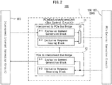
- FIG. 2 is a block diagram depicting an example of a bus control circuit in a semiconductor integrated circuit in the information processing device depicted in FIG. 1 .
- a bus control circuit (PCIe Exclusive Access Unit) 1 includes a first converter (Interconnect to PCIe Bus Bridge) 11 for converting signals from an internal connection circuit 103 to external connection circuits 106, 107 connected to a PCIe 200.
- the bus control circuit 1 includes a second converter (PCIe to Interconnect Bus Bridge) 12 for converting signals from the external connection circuits 106, 107 connected to the PCIe 200, to the internal connection circuit 103.
- the first converter 11 receives and converts an exclusive command from the internal connection circuit 103, and outputs the converted command to the external connection circuits 106, 107 connected to the PCIe 200; and the first converter 11 includes a command conversion block A-1, an exclusive response issuing block A-2, and a selector 10.
- the command conversion block A-1 is a circuit, for example, which receives an exclusive command applying to an AXI specification and including a format suitable for an exclusive control within the semiconductor integrated circuit 100 from the internal connection circuit 103, converts into an exclusive command applying to an AXI specification and including another format suitable for the PCIe specification, and outputs to the external connection circuits 106, 107.
- the exclusive response issuing blocks A-2 is a circuit, for example, which receives exclusive response information included in the exclusive command applying to the AXI specification of the internal connection circuit 103 from an exclusive command generation block B-1, and issues the exclusive response information suitable for the PCIe specification to the external connection circuits 106, 107.
- the selector 10 is a circuit for selecting an output of the command conversion block A-1 or the exclusive response issuing blocks A-2, and outputting to the PCIe 200.
- the second converter 12 receives and converts the exclusive command from PCIe 200, and outputs the converted command to the internal connection circuit 103, and the second converter 12 includes the exclusive command generation block B-1 and the exclusive response receiving block B-2.
- the exclusive command generation block B-1 is a circuit, for example, which receives an exclusive command applying to an AXI specification and including a format suitable for the PCIe specification from the external connection circuits 106, 107 connected to the PCIe 200, generates an exclusive command applying to an AXI specification and including another format suitable for an exclusive control within the semiconductor integrated circuit 100, and outputs the generated command to the internal connection circuit 103.
- the exclusive response receiving block B-2 is a circuit, for example, which receives exclusive response information for the exclusive command issued from the external connection circuits 106, 107 to the PCIe 200, and output the received command to the block A-1.
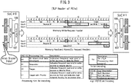
- FIG. 3 is a diagram for explaining an example of transmitting an exclusive command using a TLP header of a PCIe packet in the information processing device depicted in FIG. 1 , and for explaining the case of inputting Misc (misc (miscellaneous)) signals of the AXI.
- the Misc signals are, for example, a user signal which may be defined by a user in the AXI, and used for propagating miscellaneous information.
- FIG. 3 indicates a memory write request header in a TLP (Transaction Layer Packet) header of a PCIe packet, and a memory read and atomic operation request header.
- TLP Transaction Layer Packet
- the TLP header in the PCIe includes a structure as depicted in FIG. 3 , and performs a conversion of an exclusive access by using, for example, TH (TLP Processing Hint present) bits, which are open to the user, ST[7: 0] fields and PH (Processing Hint) bits.
- TH bits of a TLP header in a PCIe, ST[7: 0] fields and PH bits are treated as Misc signals of the AXI input to the PCIe.
- the external connection circuits 106, 107 of the SoC#0 generate TH bits of the TLP header, ST[7: 0] fields, and PH bits in the PCIe based on bit information of the Misc signals of the AXI.
- the Misc signals may include, for example, ARUSER[x: 0] and AWUSER[x: 0] of the AXI, which will be described later.
- Misc signals of the AXI are treated as the TH bits of the TLP header in the PCIe, the ST[7: 0] fields and the PH bits input to the AXI.
- the external connection circuits 106, 107 of the SoC#0 generate Misc signals of the AXI base on bit information of the TH bits of the TLP header in the PCIe, the ST[7: 0] fields and the PH bits.
- the Misc signals may include, for example, ARUSER[x: 0] and AWUSER[x: 0] of the AXI, which will be described later.
- bits treated as the Misc signals are not limited to TH bits of a TLP header in a PCIe, ST[7: 0] fields and PH bits, but the Misc signals may use other bits which are open to the user. Furthermore, it is of course that bits used for converting the exclusive access is not limited to those in the TLP header.
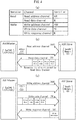
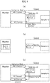
- FIG. 4 and FIG. 5 are diagrams for explaining the basic configuration of the AXI.
- an AXI includes a read address for reading (AR) channel “Read address channel” and a read data (R) channel “Read data channel”. Further, the AXI includes a write address for writing (AW) channel “Write address channel”, a write data (W) channel “Write data channel” and a write response (B) channel “Write response channel”. Therefore, the AXI includes five channels.
- FIG. 4(b) is a diagram for explaining a read operation in the AXI
- FIG. 4(c) is a diagram for explaining a write operation in the AXI. Note that, in FIG. 4(b) and FIG. 4(c) , "AXI Master” is assumed to the CPU102 of the SoC#0 depicted in FIG. 1 , and “AXI Slave” is assumed to the memory (DDR memory) 101 of the SoC#1 depicted in FIG. 1 .
- an internal connection circuit 103 of the SoC#0 a bus control circuit 1 and external connection circuits 106, 107, PCIe 200, external connection circuits 106, 107 of the SoC#1, and the like are provided.
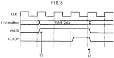
- each channel includes signals of valid (VALID) / ready (READY) / transmission information (Information) for an operation of a transaction, and information is exchanged by a handshake of VALID / READY.
- a reference CLK denotes a clock.
- a transmitting side asserts a VALID signal (T1 depicted in FIG. 5 ) indicating that information is valid
- a receiver side asserts a READY signal indicating that the receiving side may receive the valid information.
- a handshaking may be established at a specific edge of the clock when the VALID and READY signals are both high level "H".
- the transmitting side holds the Information and the VALID signal to a timing T2 depicted in FIG. 5 . In this way, an exchange of information may be completed.
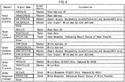
- FIG. 6 is a diagram for explaining an example of signals in the AXI.
- signals ARLOCK[1: 0], ARUSER[x: 0], RRESP[1: 0], AWLOCK[1: 0], AWUSER[x: 0] and BRESP[1: 0] which are surrounded by a thick frame in FIG. 6 may be used.
- the ARLOCK[1: 0] indicates an atomic access and is a signal (AXI3 (version 3 of the AXI) only) designating usual / exclusive / lock accesses
- the ARUSER[x: 0] is a user signal, which may be defined by a user, and is one of the above-mentioned Misc signals.
- RRESP[1: 0] indicates a read response, and is a signal indicating a result status of the read transfer. Note that a reference [x 0] indicates an arbitrary bit width.
- the AWLOCK[1: 0] indicates an atomic access and is a signal (AXI3 only) designating usually / exclusive / lock accesses
- the AWUSER[x: 0] is a user signal, which may be defined by a user, and is one of the above-mentioned Misc signals.
- the BRESP[1: 0] indicates a write response, and is a signal indicating a result status of the write transfer.
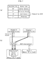
- FIG. 7 is a diagram for explaining an example of an exclusive access in the AXI.
- values "00", “01”, “10” and “11" of a 2-bit signal AxLOCK[1: 0] indicate "normal access”, “exclusive access”, “lock access” and “reserved", respectively.
- the AxLOCK[1: 0] indicates both ARLOCK[0 1] and ARLOCK[1 0].
- a value "10" of the AxLOCK[1: 0] is removed in an AXI4 (version 4 of the AXI).
- FIG. 7(b) indicates a case where accesses of a master 0 (Master 0: for example, a CPU 102 of the SoC#0) and a slave 0 (Slave 0: for example, a memory 101 of the SoC#0) are competed.
- the slave 1 (Slave 1) is, for example, the memory 101 of the SoC#1.
- FIG. 8 is a diagram for explaining a response used in the AXI.
- a response used in the AXI is four types "OKAY”, “EXOKAY”, “SLVERR” and “DECERR” which correspond to values "00", “01", “10” and “11” represented by a 2-bit RRESP[1: 0] and BRESP[1: 0].
- the "OKAY” indicates that a normal access is successful or an exclusive access is failure
- the "EXOKAY” indicates that one of an exclusive read or an exclusive write is successful
- the "SLVERR” indicates a slave error which is a notification from the slave to the master.
- the "DECERR” indicates an decoding error, or an destination address is not present in the slave, and is usually generated by an interconnect.
- FIG. 9 is a diagram for explaining an operation of an exclusive access in the AXI.
- a semaphore access read-modify-write
- a basic is a basic.
- FIG. 10 is a diagram for explaining an example of a read access operation in the information processing device depicted in FIG. 1 .
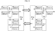
- FIG. 11 is a diagram for explaining an example of an exclusive read access operation in the information processing device depicted in FIG. 10 , and for explaining a conversion of AXI commands in the exclusive read access operation.
- a bus used to exchange commands and various information within the SoC#0 and SoC#1 is an AXI, which deals with an exclusive read access
- a bus used to exchange commands and various information between the SoC#0 and SoC#1 is a PCIe, which does not deal with the exclusive read access.
- AXI which deals with an exclusive read access
- PCIe a bus used to exchange commands and various information between the SoC#0 and SoC#1
- PCIe which does not deal with the exclusive read access.
- an exclusive read processing may be realized between two semiconductor integrated circuits (SoCs) applying to AXI specifications and each including an exclusive read function, connected by a PCIe which does not include an exclusive read function.
- SoCs semiconductor integrated circuits
- PCIe which does not include an exclusive read function
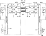
- FIG. 12 is a diagram for explaining an example of a write access operation in the information processing device depicted in FIG. 1 .
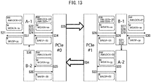
- FIG. 13 is a diagram for explaining an example of an exclusive write access operation in the information processing device depicted in FIG. 12 , and for explaining a conversion of an AXI command of an exclusive write access operation.
- a bus used for exchanging commands or various information within an SoC#0 and an SoC#1 is an AXI dealing with an exclusive write access
- a bus used for exchanging commands or various information between the SoC#0 and SoC#1 is a PCIe not dealing with an exclusive write access.
- a reference "xx" indicates write data
- "yy” indicates exclusive responses.
- exclusive write information is set to Misc signals of an AXI by the block A-1 (step S23).
- a write command including exclusive control information as header information from the PCIe#0 to the PCIe#1 (step S25)
- the normal write command (with Misc signals) is held and an exclusive write command is generated from exclusive write information of the Misc signals by the block B-1 (step S28).
- identification information for indicating an exclusive write response is issued from the block B-1 to an exclusive response issuing block A-2 based on the exclusive write response held by the block B-1 (step S32: B BRESP by "yy”).
- an exclusive write processing may be realized between two semiconductor integrated circuits (SoCs) applying to AXI specifications and each including an exclusive write function, connected by a PCIe which does not include an exclusive write function.
- SoCs semiconductor integrated circuits
- PCIe which does not include an exclusive write function.
- a propagation of an exclusive access may be possible between buses including different specifications.
- FIG. 14 is a diagram for explaining another example of an exclusive read access operation in the information processing device depicted in FIG. 10 and FIG. 11 , and for explaining an example of performing an exclusive read access operation without using Misc signals of an AXI.
- steps S4' and S6' are additionally provided to the steps S1 to S19 depicted in FIG. 11 .
- the PCIe#0 receives the normal write command, and issues a response indicating successful receipt to the block A-1.
- the block B-1 generates an exclusive read command of the AXI based on the normal read command (step S6) and the normal write command of the exclusive read information (step S6').
- an exclusive write access operation may be possible to perform without using Misc signals. Therefore, it is possible to realize an exclusive access processing without using Misc signals of a PCIe.
- FIG. 15 is a block diagram depicting another example of an information processing device according to the present embodiment, and depicting an example of an information processing device where three SoCs of AXI specifications (SoC#0, SoC#1, SoC#2) 100 are connected by a PCIe 200. Specifically, as is apparent from a comparison FIG. 15 with FIG. 1 described above, the information processing device depicted in FIG. 15 additionally includes an SoC#2 to the information processing device depicted in FIG. 1 .
- a circuit board 300 including the SoC#2 and a memory 101 corresponds to a motherboard, and two circuit boards 300 (SoC#0, SoC#1) are inserted to sockets of the mother board (SoC#2).
- SoC#0 to SoC#2 each of the SoCs (semiconductor integrated circuits) includes a number (SoC number) for identifying itself, or a port number (corresponding to a socket of the motherboard (SoC#2)) is assigned to each of the SoC#0 to SoC#2 so as to identify each circuit board 300 mounting the SoC 100.
- FIG. 15 depicts, for example, the case where the CPU 102 of the SoC#0 accesses the memory 101 connected to the SoC#1, and blocks A-1 and B-2 in a bus control circuit 1 of the SoC#0 are activated (ON). Further, two external connection circuits (106, 107) and the bus control circuit 1 are provided for the SoC#2, and in the case of accessing between the SoC#0 and SoC#1, the blocks A-1, A-2, B-1 and B-2 of the bus control circuit 1 are all inactivated (OFF). Furthermore, the number of SoCs 100 (circuit board 300) is not limited to two or three, and a larger number of SoCs (circuit board) of may be connected, as described above.
- FIG. 16 is a diagram for explaining an example of an exclusive command conversion block for a read channel in the bus control circuit depicted in FIG. 2 .
- the exclusive command conversion block A-1 includes a block A-11 for performing conversion processing of a read address (RA) channel and a block A-12 for performing conversion processing of read data (R) channel, at the time of a read access operation as described with reference to FIG. 10 and FIG. 11 .
- RA read address
- R read data
- the block A-11 receives S_A1_ARLOCK and S_A1_ARADDR from the CPU#0 (internal connection circuit 103) by the step S1 depicted in FIG. 10 and FIG. 11 , converts into D_A1_ARLOCK, D_A1_ARID[x] and D_A1_ARUSER[0], and outputs to the PCIe#0 (step S4).
- S_A1_ARLOCK and S_A1_ARADDR are used as D_A_1_ARLOCK and D_A1_ARADDR.
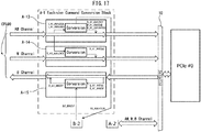
- FIG. 17 is a diagram for explaining an example of an exclusive command conversion block for a write channel in the bus control circuit depicted in FIG. 2 .
- the exclusive command conversion block A-1 includes a block A-13 for performing a conversion processing of a write address (AW) channel, a block A-14 for performing a conversion processing of write data (W) channel, and a block A-15 for performing a write response (B) channel, at the time of a write access operation as described with reference to FIG. 12 and FIG. 13 .
- the block A-13 receives S_A1_AWLOCK and S_A1_AWADDR from the CPU#0 by the step S16 depicted in FIG. 12 and FIG. 13 , converts into D_A1_AWLOCK, D_A1_AWID[x] and D_A1_AWUSER, and outputs to a selector 10 (PCIe#0) (steps S22 to S24).
- S_A1_AWLOCK and S_A1_AWADDR are used as D_A1_AWLOCK and D_A1_AWADDR.
- S_A1_AWLOCK indicating whether an exclusive access is determined to 2-bit data ("01"), however, it may be possible as one bit data (“0" or "1").
- the exclusive response receiving block B-2 outputs B2_BRESP to the block A-15.
- output signals of the exclusive response issuing block A-2 are also input to the selector 10, and the selector selects the output of the block A-2, for example, when receiving an exclusive response issuing identification signal (SS) which will be described later with reference to FIG. 21 , and otherwise, selects the output of the block A-1.
- SS exclusive response issuing identification signal
- FIG. 18 is a diagram for explaining an example of an exclusive response receiving block for a read channel in the bus control circuit depicted in FIG. 2 .
- the exclusive response receiving block B-2 includes three blocks B-21, B-22 B-23 for performing a transfer processing and conversion processing between the exclusive command conversion block A-1 and the PCIe#0, at the time of an access operation as described with reference to FIG. 10 to FIG. 13 .
- the block B-21 receives B2 _ARADDR and B2_AWADDR from the exclusive command conversion block A-1, also receives S_B2_AWADDR from an AW channel of the PCIe#0, and generates and outputs an exclusive response receiving identification signal (SR) to the block B-22.
- SR exclusive response receiving identification signal
- the block B-22 when S_B2_AWADDR is coincident with B2_ARADDR or B2_AWADDR, it is determined that the exclusive response is an exclusive command issued from the block A-1, and the block B-21 outputs an exclusive response receiving identification signal SR to the block B-22.
- the block B-22 receives S_B2_WDATA from the PCIe#0 through a W channel, converts the S_B2_WDATA into B2_RRESP and B2_BRESP based on the exclusive response receiving identification signal SR from the block B-21, and outputs to the block A-1. Specifically, when a response is confirmed as an exclusive response for the exclusive command issued from the block A-1 based on the exclusive response receiving identification signal SR, the exclusive response value on S_B2_WDATA is transferred to the block A-1 as B2_RRESP or B2_BRESP.
- the block B-23 is a block used to receive write response (B) channel information from the PCIe#0, however, the block B-23 is thin relationship with the present embodiment and descriptions thereof will be omitted.
- FIG. 19 is a diagram for explaining an example of an exclusive command generation block for the read channel in the bus control circuit depicted in FIG. 2 .
- the exclusive command generation block B-1 includes a block B-11 for performing a conversion processing of the an AR channel, and a block B-12 for performing a conversion processing of an R channel, at the time of a read access operation as described with reference to FIG. 10 and FIG. 11 .
- the block B-11 receives S_B1_ARLOCK, S_B1_ARADDR and S_B1 ARUSER from the PCIe#1 as the step S6 depicted in FIG. 10 and FIG. 11 , converts into D_B1_ARLOCK and D_B1_ARID[y], and outputs to the internal connection circuit 103 (DDR#1) (steps S7 to S10).
- FIG. 20 is a diagram for explaining an example of an exclusive command generation block for the write channel in the bus control circuit depicted in FIG. 2 .
- the exclusive command generation block B-1 includes a block B-13 for performing a conversion processing of an AW channel, a block B-14 for performing a conversion processing of a W channel, and a block B-15 for performing a conversion processing of a B channel, at the time of a write access operation as described with reference to FIG. 12 and FIG. 13 .
- the block B-13 receives S_B1_AWLOCK, S_B1_AWADDR and S_B1_AWUSER[0] from the PCIe#1 by the step 26 depicted in FIG. 12 and FIG. 13 , converts into D_B1_AWLOCK and D_B1_AWID[y], and outputs to the internal connection circuit 103 (DDR#1) (steps S27 to S30).
- FIG. 21 is a diagram for explaining an example of an exclusive response issuing block for the write channel in the bus control circuit depicted in FIG. 2 .
- an exclusive response issuing blocks A-2 includes a block A-21 for performing a conversion processing of an AW channel, and a block A-23 for performing a conversion processing of a W channel, at the time of a write access operation as described with reference to FIG. 12 and FIG. 13 .
- the block A-21 receives B1_ARADDR and B1_AWADDR from the exclusive command generation block B-1 by the step S32 depicted in FIG. 12 and FIG. 13 , converts into D_A2_AWADDR, and outputs to a selector 10 (PCIe#1) (step S13). Specifically, the block A-21 issues an AW command for an exclusive response to an AW channel (selector 10) by transferring B1_ARADDR or B1_AWADDR as D_A2_AWADDR, when receiving an exclusive response issuing identification signal SS from a block A-22 which will be described later.
- the block A-22 receives B1_RRESP and B1_BRESP from the block B-1, converts into D_A2_WDATA, and outputs to a selector (PCIe#1). Specifically, the block A-22 transfers an exclusive response issuing identification signal SS to the AW channel and the selector 10 so as to issue an exclusive response, when the block A-22 receives B1_RRESP or B1_BRESP. Further, a value of B1_RRESP or B1_BRESP is converted as an exclusive value of D_A2_WDATA. Note that an explanation of the block A-23 is omitted, since the relationship is thin.
- the selector 10 is provided between the PCIe#1, and the exclusive command conversion block A-1 and the exclusive responses issuing blocks A-2, and signals selected by the selector 10 are transferred between the PCIe#1, and the block A-1 or A-2. Specifically, in the case of receiving an exclusive response issuing identification signal SS, the selector 10 selects a path A-2, and otherwise, the selector 10 selects a path A-1.
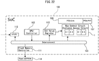
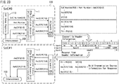
- FIG. 22 and FIG. 23 are diagrams for explaining a method of generating / restoring header information including ST bits [7: 0] in the information processing device with reference to FIG. 1 and FIG. 2 , and for explaining an acquisition of information of SoC numbers or port numbers indicated with reference to FIG. 15 .
- a memory DDR memory 101
- memory connection circuits 104, 105
- IP macros 1028 and the like are omitted, since the relationship is thin.
- an SoC 100 includes, for example, a flash memory controller 111, an electronic fuse (eFUSE) 112 and the set value register 113, in addition to the SoC described with reference to FIG. 1 .
- the flash memory controller 111 controls, for example, the flash memory (or, eEPROM) 114 provided outside of the 114 controls the flash memory controller 111.
- the flash memory controller 111 includes an electronic fuse (eFUSE) 112 and a set value register 113. Note that the flash memory controller 111 controls, for example, a flash memory or a nonvolatile memory (Electrically Erasable Programmable Read-Only Memory: Flash / eEPROM: external memory) 114 provided outside of the flash memory controller 111.
- eFUSE electronic fuse
- Flash / eEPROM external memory
- the external memory (Flash / EEPROM) 114 or electronic fuse 112 stores previously SoC numbers or port numbers, for example, when power is turned ON, a CPU (or controller) 102 reads out values stored in the external memory 114 or the electronic fuse 112, and copies to a setting value register 113. Further, the values copied to the setting value register 113 are read out by the bus control circuit (exclusive access circuit) 1, and in a state where each of the SoCs is identified, an exclusive access processing described above is performed. Note that the CPU 102 may set the values read out from the external memory 114 or the electronic fuses 112 directly to the bus control circuit 1 without passing through the setting value register 113.
- ST bit (ST[7: 0]) in the PCIe TLP header described with reference to FIG. 3 may be used.
- the bus control circuit (PCIe Exclusive Access Unit) 1 reads out, for example, SoC numbersof the SoC#0 (SoC Number [5: 0]) and port numbers from the setting value register 113.
- AxLOCK[1: 0] and AxADDR[31: 0] are read out through the internal connection circuit (Interconnect) 103, for example, by performing the process described above, and AxUSER[7: 0], AxUSER[10: 8] and AxADDR[31 0] may be output to the PCIe #.
- data of the SoC#0 is converted (generated) as, for example, SoC Number [5: 0] + Port Number + AxLOCK[1: 0] ⁇ AxUSER[7: 0] ⁇ ST[7: 0], and converted to header information by performing conversions as AxLOCK[1: 0] ⁇ AxUSER[10: 8] ⁇ TH + PH[1: 0].
- AxLOCK is, for example, a two-bot signal such as AxLOCK[1: 0], however, AxLOCK may be one-bit signal, for example, "01" indicates an exclusive access and "00" indicates a normal access.
- AxUSER[10: 8] which may transfer information of 3 bits, for example, in this case, one bit is fixed and other two bits may be used.
- information embedded in ST[7: 0], TH and PH[1: 0] of a TLP header in the PCIe is, for example, recovered in the SoC#1.
- ST[7: 0] ⁇ AxUSER[7: 0]] response for transmission source information holding to recover the information embedded in the TLP header in the PCIe.
- AxUSER[7: 0] AxUSER[10: 8] and AxADDR[31: 0] is input from the PCIe#1 to the bus control circuit 1, and AxLOCK[1: 0] and AxADDR[31: 0] are output from the bus control circuit to the 1 internal connection circuit 103.
- a setting value register 113 may be also provided, and steps of a reverse direction (from SoC#1 to SoC#0) in the above descriptions may be possible to perform.
- steps of a reverse direction from SoC#1 to SoC#0
- the use of ST[7: 0], TH and PH[1: 0] of the TLP header described above is only an example, and other bit fields of the header or appropriate bits fields in each bus specification may be also possible to use.
Landscapes
- Engineering & Computer Science (AREA)
- Theoretical Computer Science (AREA)
- General Engineering & Computer Science (AREA)
- Physics & Mathematics (AREA)
- General Physics & Mathematics (AREA)
- Computer Hardware Design (AREA)
- Bus Control (AREA)
- Memory System (AREA)
- Information Transfer Systems (AREA)
Abstract
Description
- The present invention relates to a bus control circuit, a semiconductor integrated circuit, a circuit board, an information processing device and a bus control method.
- Recently, in information processing systems such as a server or the like, for example, a plurality of semiconductor integrated circuits or circuit boards applying to different bus specifications have been used. In the semiconductor integrated circuits applying to the different bus specifications, for example, there are sometimes difficult to reloaded information of a first bus specification to information of a second bus specification which is different from the first bus specification.
- Concretely, in an SoC (System on a Chip) including an AXI (REGISTERED TRADEMARK) (Advanced eXtensible Interface) specification, for example, an exclusive control of a memory access in the SoC has been implemented so as to ensure a secure and software sequence of a common resource in an OS (Operating System).
- Specifically, when executing one OS by using an SoC including a plurality of CPUs (Central Processing Units) or even when ensuring a common resource in different OSs, it may be required to implement an exclusive control beyond a chip (semiconductor integrated circuit). However, even when requiring an exclusive control beyond such a chip, a propagation function of the exclusive control may not previously provided between the chips applying to different bus specifications.
- Here, the AXI (REGISTERED TRADEMARK) is included in an AMBA (REGISTERED TRADEMARK) (Advanced Microcontroller Bus Architecture), which is a general term for an on-chip interconnect specification, for example, together with an AHB (REGISTERED TRADEMARK) (Advanced High-performance Bus) and an APB (REGISTERED TRADEMARK) (Advanced Peripheral Bus). Further, for example, an OCP (Open Core Protocol), a PIF (Processor InterFace), etc., may be known as specifications other than the AMBA.
- Incidentally, in the prior art, for example, various techniques have been proposed for an exclusive control in a multiprocessor system.
-
- [Patent Document 1] Japanese Laid-open Patent Publication No.
H06(1994)-110844 - [Patent Document 2] Japanese Laid-open Patent Publication No.
H08(1996)-161228 - As described above, between chips including (applying to) different bus specifications, an exclusive control function may not previously provided. For example, a propagation function of an exclusive control has not been previously prepared between a semiconductor integrated circuit including a PCIe (REGISTERED TRADEMARK) (Peripheral Component Interconnect Express) specification which is widely used, and an SoC including an AXI specification.
- Such no propagation function of the exclusive control is provided between semiconductor integrated circuits, circuit boards or the like including different bus specifications is the same as between semiconductor integrated circuits, circuit boards or the like to which various other bus specifications may be applied.
- Here, the present invention is not limited to an exclusive control propagation between a PCIe specification and an AXI specification, but also applied to an exclusive control propagation between semiconductor integrated circuits, circuit boards or the like including different bus specifications. Specifically, the present invention may be possible to apply to an exclusive control propagation between a semiconductor integrated circuit or the like including a PCIe and a semiconductor integrated circuit or the like including an AMBA such as an AXI, an AHB and an APB or a semiconductor integrated circuit or the like including an OCP or a PIF.
- According to an aspect of the embodiments, there is provided a bus control circuit configured to transfer an exclusive command between a first bus specification and a second bus specification by mutually converting a first exclusive command including a first format and applying to the first bus specification which deals with an exclusive access, and a second exclusive command including a second format and applying to the second bus specification which is different from the first bus specification and does not deal with the exclusive access, includes an exclusive command conversion circuit, an exclusive command generation circuit, an exclusive response issuing circuit, and an exclusive response receiving circuit.
- The exclusive command conversion circuit is configured to receive the first exclusive command, convert the first exclusive command into the second exclusive command and output the second exclusive command, when converting from the first exclusive command to the second exclusive command, and the exclusive command generation circuit is configured to receive the second exclusive command and generate the first exclusive command, when converting from the second exclusive command to the first exclusive command.
- The exclusive response issuing circuit configured to issue exclusive response information for the second exclusive command, when converting from the second exclusive command to the first exclusive command, and the exclusive response receiving circuit is configured to receive exclusive response information for the second exclusive command, when converting from the first exclusive command to the second exclusive command.
- According to embodiments of a bus control circuit, a semiconductor integrated circuit, a circuit board, an information processing device and a bus control method disclosed herein, an exclusive access propagation between buses including different specifications may be possible.
-
-
FIG. 1 is a block diagram depicting an example of an information processing device according to the present embodiment. -
FIG. 2 is a block diagram depicting an example of a bus control circuit in a semiconductor integrated circuit in the information processing device depicted inFIG. 1 . -
FIG. 3 is a diagram for explaining an example of transmitting an exclusive command using a TLP header of a PCIe packet in the information processing device depicted inFIG. 1 . -
FIG. 4 is a diagram for explaining a basic configuration of an AXI (Part 1). -
FIG. 5 is a diagram for explaining the basic configuration of the AXI (Part 2). -
FIG. 6 is a diagram for explaining an example of signals in the AXI. -
FIG. 7 is a diagram for explaining an example of an exclusive access in the AXI. -
FIG. 8 is a diagram for explaining a response used in the AXI. -
FIG. 9 is a diagram for explaining an operation of an exclusive access in the AXI. -
FIG. 10 is a diagram for explaining an example of a read access operation in the information processing device depicted inFIG. 1 . -
FIG. 11 is a diagram for explaining an example of an exclusive read access operation in the information processing device depicted inFIG. 10 . -
FIG. 12 is a diagram for explaining an example of a write access operation in the information processing device depicted inFIG. 1 . -
FIG. 13 is a diagram for explaining an example of an exclusive write access operation in the information processing device depicted inFIG. 12 . -
FIG. 14 is a diagram for explaining another example of an exclusive read access operation in the information processing device depicted inFIG. 10 andFIG. 11 . -
FIG. 15 is a block diagram depicting another example of an information processing device according to the present embodiment. -
FIG. 16 is a diagram for explaining an example of an exclusive command conversion block for a read channel in the bus control circuit depicted inFIG. 2 . -
FIG. 17 is a diagram for explaining an example of an exclusive command conversion block for a write channel in the bus control circuit depicted inFIG. 2 . -
FIG. 18 is a diagram for explaining an example of an exclusive response receiving block for a read channel in the bus control circuit depicted inFIG. 2 . -
FIG. 19 is a diagram for explaining an example of an exclusive command generation block for the read channel in the bus control circuit depicted inFIG. 2 . -
FIG. 20 is a diagram for explaining an example of an exclusive command generation block for the write channel in the bus control circuit depicted inFIG. 2 . -
FIG. 21 is a diagram for explaining an example of an exclusive response issuing block for the write channel in the bus control circuit depicted inFIG. 2 . -
FIG. 22 is a diagram for explaining a method of generating / restoring header information including ST bits [7: 0] in the information processing device with reference toFIG. 1 andFIG. 2 (Part 1). -
FIG. 23 is a diagram for explaining the method of generating / restoring header information including ST bits [7: 0] in the information processing device with reference toFIG. 1 andFIG. 2 (Part 2). - Hereinafter, embodiments of a bus control circuit, a semiconductor integrated circuit, a circuit board, an information processing device and a bus control method will be described in detail with reference to the accompanying drawings.
FIG. 1 is a block diagram depicting an example of an information processing device according to the present embodiment. InFIG. 1 ,reference numeral 100 denotes an SoC (semiconductor integrated circuit), and 200 denotes a PCIe (REGISTERED TRADEMARK) bus. - In
FIG. 1 , two SoCs (SoC# 0, SoC#1) 100 are connected by a PCIe bus (PCIe) 200 as an example, however, the number ofSoCs 100 is not limited to two, and a specification of theSoC 100 is not limited to the AXI. Further, the bus connecting the plurality ofSoCs 100 is not limited to thePCIe 200. - Note that, the SoC 100 is formed as a single semiconductor integrated circuit (chip), but the SoC 100 may also be formed as a plurality of chips. Furthermore, in
FIG. 1 , acircuit board 300 is formed by the SoC 100 (controller) and amemory 101, and an information processing device (for example, a server) is formed by a plurality ofcircuit boards 300, but the present embodiment may be widely applied to various configurations. - As depicted in
FIG. 1 , eachcircuit board 300 includes anSoC 100 and a memory (for example, DDR (Double-Data-Rate) Memory) 101. Thecircuit board 300 may include various chips (semiconductor integrated circuits). The SoC 100 includes a bus control circuit (exclusive access circuit) 1, aCPU 102, an internal connection circuit (Interconnect) 103, memory connection circuits (104, 105), external connection circuits (106, 107), and various IPs ((IP: Intellectual Property) cores, IP macros) 108. - The memory connection circuit includes, for example, a memory control circuit (DDR Controller) 104 for controlling a connection with a memory (DDR Memory) 101, and an interface IP macro (DDR PHY) 105 of the
memory 101. The external connection circuit includes, for example, a link control circuit (PCIe Link) 106 for controlling a connection (link) with the other SoC 100 (circuit board 300) throuhg aPCIe 200, and an interface IP macro (physical layer of PCIe: PCIe PHY) 107. - The
internal connection circuit 103 exchanges signals (data and commands) between theCPU 102, and the memory control circuit (DDR Controller) 104, thebus control circuit 1 and theIP macros 108 based on the AXI specification. Further, theCPU 102, thememory control circuit 104, theIP macros 108 and the like may constitute an internal circuit of the AXI specification (internal bus specification). Here, thebus control circuit 1 receives and converts signals of the AXI specification, and outputs to the PCIe (external bus) 200 through the external connection circuit (linkcontrol circuit 106 and the physical layer 107). Further, thebus control circuit 1 converts signals input from thePCIe 200 through the external connection circuits (106, 107), and outputs to the internal connection circuit 103 (CPU 102, thememory control circuit 104 and theIP macros 108, etc.) of the AXI specification. - The
bus control circuit 1 includes an exclusive command conversion block A-1, an exclusive response issuing block A-2, an exclusive command generation block B-1 and an exclusive response receiving block B-2, and is provided on each of theSoCs 100. - Here, when the exclusive command is output from one
SoC# 0 through thePCIe 200 to the other SoC#1 (when an exclusive access is issued from theSoC# 0 to the SoC#1), blocks A-1, A-2, B-1 and B-2 in each of theSoCs 100 operate as follows. In oneSoC# 0, the blocks A-1 and B-2 are turned ON (activated), and the blocks A-2 and B-1 are turned OFF (inactivated); and in theother SoC# 1, the blocks A-1 and B-2-are turned OFF, and the blocks A-2 and B-1 are turned ON. - Note that the exclusive access indicates an access, for example, in the case of sharing resources (memory, etc.) and wherein, while a specific portion (specific address of the memory, etc.) of the shared resources is accessed by the
SoC# 0, the specific portion the shared resources may not be accessed by theSoC# 0 so as to maintain an integrity of the shared resources. Further, the exclusive command indicates a command for requesting the exclusive access, for example, including an exclusive read command and an exclusive write command. - On the other hand, a normal access indicates an access, for example, not including the above exclusive control. Further, a normal command indicates a command for requesting the normal access, for example, including a normal read command and a normal write command.
-
FIG. 2 is a block diagram depicting an example of a bus control circuit in a semiconductor integrated circuit in the information processing device depicted inFIG. 1 . As depicted inFIG. 2 , in each semiconductor integrated circuit (SoC# 0, SoC#1) 100, a bus control circuit (PCIe Exclusive Access Unit) 1 includes a first converter (Interconnect to PCIe Bus Bridge) 11 for converting signals from aninternal connection circuit 103 toexternal connection circuits PCIe 200. Further, thebus control circuit 1 includes a second converter (PCIe to Interconnect Bus Bridge) 12 for converting signals from theexternal connection circuits PCIe 200, to theinternal connection circuit 103. - The
first converter 11 receives and converts an exclusive command from theinternal connection circuit 103, and outputs the converted command to theexternal connection circuits PCIe 200; and thefirst converter 11 includes a command conversion block A-1, an exclusive response issuing block A-2, and aselector 10. - Here, the command conversion block A-1 is a circuit, for example, which receives an exclusive command applying to an AXI specification and including a format suitable for an exclusive control within the semiconductor integrated
circuit 100 from theinternal connection circuit 103, converts into an exclusive command applying to an AXI specification and including another format suitable for the PCIe specification, and outputs to theexternal connection circuits - Further, the exclusive response issuing blocks A-2 is a circuit, for example, which receives exclusive response information included in the exclusive command applying to the AXI specification of the
internal connection circuit 103 from an exclusive command generation block B-1, and issues the exclusive response information suitable for the PCIe specification to theexternal connection circuits selector 10 is a circuit for selecting an output of the command conversion block A-1 or the exclusive response issuing blocks A-2, and outputting to thePCIe 200. - The
second converter 12 receives and converts the exclusive command fromPCIe 200, and outputs the converted command to theinternal connection circuit 103, and thesecond converter 12 includes the exclusive command generation block B-1 and the exclusive response receiving block B-2. - Here, the exclusive command generation block B-1 is a circuit, for example, which receives an exclusive command applying to an AXI specification and including a format suitable for the PCIe specification from the
external connection circuits PCIe 200, generates an exclusive command applying to an AXI specification and including another format suitable for an exclusive control within the semiconductor integratedcircuit 100, and outputs the generated command to theinternal connection circuit 103. Further, the exclusive response receiving block B-2 is a circuit, for example, which receives exclusive response information for the exclusive command issued from theexternal connection circuits PCIe 200, and output the received command to the block A-1. - Next, an example using a PCIe (REGISTERED TRADEMARK) and an AXI (REGISTERED TRADEMARK) as different two bus specifications for converting an exclusive access in the present embodiment will be explained with reference to
FIG. 3 to FIG. 9 , and thereafter, the present embodiment will be explained in detail with reference toFIG. 10 to FIG. 23 . -
FIG. 3 is a diagram for explaining an example of transmitting an exclusive command using a TLP header of a PCIe packet in the information processing device depicted inFIG. 1 , and for explaining the case of inputting Misc (misc (miscellaneous)) signals of the AXI. Here, the Misc signals are, for example, a user signal which may be defined by a user in the AXI, and used for propagating miscellaneous information. Note thatFIG. 3 indicates a memory write request header in a TLP (Transaction Layer Packet) header of a PCIe packet, and a memory read and atomic operation request header. - As described with reference to
FIG. 1 , for example, when an exclusive access is issued from oneSoC# 0 to theother SoC# 1, in theSoC# 0, the blocks A-1 and B-2 are turned ON, and in theSoC# 1, the blocks A-2 and B-1 are turned ON. Here, the TLP header in the PCIe includes a structure as depicted inFIG. 3 , and performs a conversion of an exclusive access by using, for example, TH (TLP Processing Hint present) bits, which are open to the user, ST[7: 0] fields and PH (Processing Hint) bits. Note that, in the present specification, for example, an example of using a TLP header as a bit field in the PCIe incorporating an exclusive command in the AXI will be explained, however, this is merely an example, and various types of bit fields in the PCIe specification may be used. - Specifically, in the
SoC# 0, TH bits of a TLP header in a PCIe, ST[7: 0] fields and PH bits are treated as Misc signals of the AXI input to the PCIe. Theexternal connection circuits SoC# 0 generate TH bits of the TLP header, ST[7: 0] fields, and PH bits in the PCIe based on bit information of the Misc signals of the AXI. The Misc signals may include, for example, ARUSER[x: 0] and AWUSER[x: 0] of the AXI, which will be described later. - Further, in the
SoC# 1, Misc signals of the AXI are treated as the TH bits of the TLP header in the PCIe, the ST[7: 0] fields and the PH bits input to the AXI. PCIe, Here, theexternal connection circuits SoC# 0 generate Misc signals of the AXI base on bit information of the TH bits of the TLP header in the PCIe, the ST[7: 0] fields and the PH bits. The Misc signals may include, for example, ARUSER[x: 0] and AWUSER[x: 0] of the AXI, which will be described later. - Note that bits treated as the Misc signals are not limited to TH bits of a TLP header in a PCIe, ST[7: 0] fields and PH bits, but the Misc signals may use other bits which are open to the user. Furthermore, it is of course that bits used for converting the exclusive access is not limited to those in the TLP header.
-
FIG. 4 andFIG. 5 are diagrams for explaining the basic configuration of the AXI. As depicted inFIG. 4(a) , an AXI includes a read address for reading (AR) channel "Read address channel" and a read data (R) channel "Read data channel". Further, the AXI includes a write address for writing (AW) channel "Write address channel", a write data (W) channel "Write data channel" and a write response (B) channel "Write response channel". Therefore, the AXI includes five channels. -
FIG. 4(b) is a diagram for explaining a read operation in the AXI andFIG. 4(c) is a diagram for explaining a write operation in the AXI. Note that, inFIG. 4(b) and FIG. 4(c) , "AXI Master" is assumed to the CPU102 of theSoC# 0 depicted inFIG. 1 , and "AXI Slave" is assumed to the memory (DDR memory) 101 of theSoC# 1 depicted inFIG. 1 . - Further, between the "AXI Master" and the "AXI Slave", an
internal connection circuit 103 of theSoC# 0, abus control circuit 1 andexternal connection circuits PCIe 200,external connection circuits SoC# 1, and the like are provided. - As depicted in
FIG. 4(b) , when data from the "AXI Master" to the "AXI Slave" (memory 101 in the SoC#1) is read, "AR" and "R" depicted inFIG. 4(a) are used. Further, as depicted inFIG. 4(c) , when data from the "AXI Master" is written to the "AXI Slave", "AW", "W" and "B" depicted inFIG. 4(a) are used. - As depicted in
FIG. 5 , each channel includes signals of valid (VALID) / ready (READY) / transmission information (Information) for an operation of a transaction, and information is exchanged by a handshake of VALID / READY. Here, a reference CLK denotes a clock. - First, a transmitting side asserts a VALID signal (T1 depicted in
FIG. 5 ) indicating that information is valid, and a receiver side asserts a READY signal indicating that the receiving side may receive the valid information. For example, a handshaking may be established at a specific edge of the clock when the VALID and READY signals are both high level "H". Note that the transmitting side holds the Information and the VALID signal to a timing T2 depicted inFIG. 5 . In this way, an exchange of information may be completed. -
FIG. 6 is a diagram for explaining an example of signals in the AXI. In this embodiment, for example, signals ARLOCK[1: 0], ARUSER[x: 0], RRESP[1: 0], AWLOCK[1: 0], AWUSER[x: 0] and BRESP[1: 0] which are surrounded by a thick frame inFIG. 6 may be used. Here, the ARLOCK[1: 0] indicates an atomic access and is a signal (AXI3 (version 3 of the AXI) only) designating usual / exclusive / lock accesses, and the ARUSER[x: 0] is a user signal, which may be defined by a user, and is one of the above-mentioned Misc signals. Further, RRESP[1: 0] indicates a read response, and is a signal indicating a result status of the read transfer. Note that a reference [x 0] indicates an arbitrary bit width. - Further, the AWLOCK[1: 0] indicates an atomic access and is a signal (AXI3 only) designating usually / exclusive / lock accesses, and the AWUSER[x: 0] is a user signal, which may be defined by a user, and is one of the above-mentioned Misc signals. Further, the BRESP[1: 0] indicates a write response, and is a signal indicating a result status of the write transfer.
-
FIG. 7 is a diagram for explaining an example of an exclusive access in the AXI. As depicted inFIG. 7(a) , values "00", "01", "10" and "11" of a 2-bit signal AxLOCK[1: 0] indicate "normal access", "exclusive access", "lock access" and "reserved", respectively. Note that the AxLOCK[1: 0] indicates both ARLOCK[0 1] and ARLOCK[1 0]. Further, a value "10" of the AxLOCK[1: 0] is removed in an AXI4 (version 4 of the AXI). -
FIG. 7(b) indicates a case where accesses of a master 0 (Master 0: for example, aCPU 102 of the SoC#0) and a slave 0 (Slave 0: for example, amemory 101 of the SoC#0) are competed. Note that the slave 1 (Slave 1) is, for example, thememory 101 of theSoC# 1. - As depicted in
FIG. 7(b) , when accesses a specific address (of thememory 101 in the SoC#0) is competed by themaster 0 and theslave 0, it is possible to realize by, for example, a semaphore type processing. Here, so as to realize an exclusive access, an exclusive access monitor may be required to provide for the slave 0 (memory 101 of the SoC#0). Further, the exclusive access monitor for the Slave depicted inFIG. 7(b) , monitors an address for accessing anSlave 0, for example, during an exclusive access from aMaster 0 to theSlave 0, aMaster 1 may be possible to access another address of theSlave 0. -
FIG. 8 is a diagram for explaining a response used in the AXI. As depicted inFIG. 8 , for example, a response used in the AXI is four types "OKAY", "EXOKAY", "SLVERR" and "DECERR" which correspond to values "00", "01", "10" and "11" represented by a 2-bit RRESP[1: 0] and BRESP[1: 0]. - Here, the "OKAY" indicates that a normal access is successful or an exclusive access is failure, the "EXOKAY" indicates that one of an exclusive read or an exclusive write is successful, and the "SLVERR" indicates a slave error which is a notification from the slave to the master. Further, the "DECERR" indicates an decoding error, or an destination address is not present in the slave, and is usually generated by an interconnect.
- Specifically, in the case of a write (writing), a single response is returned for an entire burst, and in the case of a read (reading), a response is returned for each data transfer in the burst. Here, it may be required to be possible to return different responses for each data transfer, and to perform required number of transfer operations even if an error occurs during the transfer operations.
-
FIG. 9 is a diagram for explaining an operation of an exclusive access in the AXI. Here, in an operation of the exclusive access, a semaphore access (read-modify-write) is a basic. - As depicted in
FIG. 9(a) , when the master performs an exclusive read (ARLOCK[0: 1] = "01"), the exclusive monitor stores an address and an ID, and the slave returns read data to the master by the "EXOKAY". Note that the slave, which is not dealing with an exclusive access, returns the "OKAY" to the master so as to notify that the slave is not compatible with the exclusive access. - As depicted in
FIG. 9(b) , when the master performs a modifier (modify) of data, while the exclusive monitor monitors whether or not a semaphore area is rewritten by another master. Note that the exclusive monitor continues a monitoring operation until causing a write operation from another master (ID) or an exclusive read operation to another address. - As depicted in
FIG. 9(c) , when the master performs an exclusive write (AWLOCK[0: 1] = "01") to after updated data, while the exclusive monitor continuously monitors the same address, an exclusivity is guaranteed, a write operation is performed, and the "EXOKAY" is returned. Further, if the exclusive monitor does not monitor the address, since the exclusivity is not guaranteed, the write operation is not performed, and the "OKAY" is returned. - Incidentally, since an exclusive control function is not provided for the PCIe, for example, in a system (information processing device) connected to two
SoC# 0 andSoC# 1 applying to the AXI, it is difficult to perform an appropriate exclusive control. -
FIG. 10 is a diagram for explaining an example of a read access operation in the information processing device depicted inFIG. 1 .FIG. 11 is a diagram for explaining an example of an exclusive read access operation in the information processing device depicted inFIG. 10 , and for explaining a conversion of AXI commands in the exclusive read access operation. - In
FIG. 10 andFIG. 11 , a bus used to exchange commands and various information within theSoC# 0 andSoC# 1 is an AXI, which deals with an exclusive read access, and a bus used to exchange commands and various information between theSoC# 0 andSoC# 1 is a PCIe, which does not deal with the exclusive read access. Note that, inFIG. 11 , "xxxx" indicates read data, "yy" indicates exclusive responses. Further, ARUSER[x: 0] (for example, exclusive access = "1") are used as Misc signals. - As depicted in
FIG. 10 andFIG. 11 , first, an exclusive read access (exclusive read command) is issued from a CPU 102 (CPU#0) of the SoC#0 (step S1), and an exclusive read command is stored in an exclusive command conversion block A-1 (step S2: AR ARLOCK = "01"). Next, exclusive read information is set to Misc signals of the AXI by the block A-1 (step S3: AR ARUSER = "1"). Further, a normal read command (with Misc signals) is issued from the block A-1 (step S4: AR ARLOCK = "00", ARUSER = "1"), for example, to an external connection circuit (linkcontrol circuit 106 and the PCIe PHY 107: PCIe#0) in theSoC# 0. - Further, a read command including exclusive control information in header information is issued from the PCIe#0 (external connection circuit of the SoC#0) to the PCIe#1 (external connection circuit of the SoC#1) (step S5), and a normal read command (with Misc signals) is issued from the
PCIe# 1 to an exclusive command generation block B-1 (step S6: AR ARLOCK = "00", ARUSER = "1"). Further, the block B-1 holds the normal read command (with Misc signals) (step S7), and generates an exclusive read command from the exclusive read information of the Misc signals (step S8). - Next, an exclusive read command is issued from the block B-1 in a
memory 101 of the SoC#1 (DDR#1) (step S9: AR ARLOCK = "01"), theDDR# 1 issues an exclusive read response (step S10), and the exclusive read response is held by the block B-1 (step S11: R RDATA = "xxxx", RRESP = "yy"). - Further, read data (Read Data) is output from the block B-1 to the
PCIe# 1 as a response of the normal read command (step S12: R RDATA = "xxxx", RRESP = "00"), and identification information (exclusive read response information) for indicating an exclusive read response is issued from the block B-1 to the exclusive response issuing blocks A-2 based on the exclusive read response held by the block B-1 (step S13: R RRESP = "yy"). In addition, a normal write command where exclusive read response information is as write data (Write Data) is issued from the block A-2 to thePCIe# 1, and thePCIe# 1 receives the normal write command and issues a response indicating a successful of the normal write to the block A-2 (step S14: AW AWLOCK = "00", W WDATA = "yy", B BRESP = "00"). - Furthermore, read data (Read Data) / write data (Write Data) is transferred from the
PCIe# 1 to the PCIe#0 (step S15), and a read data transfer for the normal read command is performed from thePCIe# 0 to the block A-1 (step S16: R RDATA = "xxxx", RRESP = "00"). Further, a normal write command where exclusive read response information is as write data is issued from thePCIe# 0 to the block B-2, and the block B-2 receives the normal write command and issues a response indicating a successful of the normal write to the PCIe#0 (step S17: AW AWLOCK = "00", W WDATA = "yy", B BRESP = "00"). In addition, the exclusive read response information is transferred from the block B-2 to the block A-1 (step S18: W WDATA = "yy"), the read data / exclusive read response information are merged by the block A-1, and an exclusive read response is transferred to the CPU#0 (step S19: R RDATA = "xxxx", RRESP = "yy"). - As described above, for example, an exclusive read processing may be realized between two semiconductor integrated circuits (SoCs) applying to AXI specifications and each including an exclusive read function, connected by a PCIe which does not include an exclusive read function. Specifically, a propagation of an exclusive access may be possible between buses including different specifications.
-
FIG. 12 is a diagram for explaining an example of a write access operation in the information processing device depicted inFIG. 1 .FIG. 13 is a diagram for explaining an example of an exclusive write access operation in the information processing device depicted inFIG. 12 , and for explaining a conversion of an AXI command of an exclusive write access operation. - In
FIG. 12 andFIG. 13 , a bus used for exchanging commands or various information within anSoC# 0 and anSoC# 1 is an AXI dealing with an exclusive write access, and a bus used for exchanging commands or various information between theSoC# 0 andSoC# 1 is a PCIe not dealing with an exclusive write access. Note that, inFIG. 13 , a reference "xx" indicates write data, "yy" indicates exclusive responses. Further, AWUSER[x: 0] is used for Misc signals (for example, exclusive access = "1"). - As depicted in
FIG. 12 andFIG. 13 , first, an exclusive write access (exclusive write command) is issued from a CPU#0 (CPU 102 of the SoC#0) (step S21), and the exclusive write comand is held in an exclusive command conversion block A-1 (step S22: AW AWLOCK = "01", W WDATA = "xx"). Next, exclusive write information is set to Misc signals of an AXI by the block A-1 (step S23). Further, a normal write command (with Misc signals) is issued from the block A-1, for example, to a PCIe#0 (external connection circuits - Furthermore, a write command including exclusive control information as header information from the
PCIe# 0 to the PCIe#1 (step S25), a the normal write command (with Misc signals) is issued from thePCIe# 1 to an exclusive command generation block B-1, and the block B-1 receives the normal write command and issues a response indicating successful receipt (step S26: AW AWLOCK = "00", AWUSER = "1", W WDATA = "xx", B BRESP = "00"). In addition, the normal write command (with Misc signals) is held and an exclusive write command is generated from exclusive write information of the Misc signals by the block B-1 (step S28). - Next, an exclusive write command is issued from the block B-1 to a DDR#1 (
memory 101 of the SoC#1) (step S29: AW AWLOCK = "01", W WDATA = "xx"), theDDR# 1 issues an exclusive write response (step S30), and the exclusive write response is held by the block B-1 (step S31: B BRESP "yy"). - Further, identification information (exclusive write response information) for indicating an exclusive write response is issued from the block B-1 to an exclusive response issuing block A-2 based on the exclusive write response held by the block B-1 (step S32: B BRESP by "yy"). In addition, a normal write command where exclusive write response information is as write data (Write Data) is issued from the block A-2 to the
PCIe# 1, and thePCIe# 1 receives the normal write command and issues a response indicating a successful of the normal write to the block A-2 (step S33: AW AWLOCK = "00", W WDATA = "yy", B BRESP = "00"). - Furthermore, write data is transferred from the
PCIe# 1 to the PCIe#0 (step S34), a normal write command where exclusive write response information is as write data is issued from thePCIe# 0 to an exclusive response receiving block B-2, and the block B-2 receives the normal write command and issues a response indicating a successful of the normal write to the PCIe#0 (step S35: AW AWLOCK = "00", W WDATA = "yy", B BRESP = "00"). In addition, the exclusive write response information is transferred from the block B-2 to the block A-1 (step S36), and the exclusive write response is transferred to theCPU# 0 by the block A-1 (step S37: B BRESP = "yy"). - As described above, for example, an exclusive write processing may be realized between two semiconductor integrated circuits (SoCs) applying to AXI specifications and each including an exclusive write function, connected by a PCIe which does not include an exclusive write function. Specifically, a propagation of an exclusive access may be possible between buses including different specifications.
-
FIG. 14 is a diagram for explaining another example of an exclusive read access operation in the information processing device depicted inFIG. 10 andFIG. 11 , and for explaining an example of performing an exclusive read access operation without using Misc signals of an AXI. - As is apparent from a comparison
FIG. 14 withFIG. 11 described above, in a modified embodiment where an exclusive read access operation is performed without using Misc signals, steps S4' and S6' are additionally provided to the steps S1 to S19 depicted inFIG. 11 . - Specifically, a step S4' is performed in addition to the step S4 (AR ARLOCK = "00", ARUSER = "1") where a normal read is issued from the exclusive command conversion block A-1 to the PCIe. In the step S4', exclusive read information is issued as a normal write command of the AXI from the block A-1 to the PCIe by, for example, AR ARLOCK = "00", ARUSER = "1". Further, the
PCIe# 0 receives the normal write command, and issues a response indicating successful receipt to the block A-1. - Further, a step S6' is performed in addition to the step S6 (AR ARLOCK = "00", ARUSER = "1") where a normal read is issued from the
PCIe# 1 to an exclusive command generation block B-1. In the step S6', exclusive read information is issued as a normal write command of the AXI from thePCIe# 1 to the block B-1 by, for example, AW AWLOCK = "00", W WDATA = "1", and the block B-1 receives the normal write command, and issues a response indicating successful receipt to thePCIe# 1. - Furthermore, the block B-1 generates an exclusive read command of the AXI based on the normal read command (step S6) and the normal write command of the exclusive read information (step S6'). Similarly, an exclusive write access operation may be possible to perform without using Misc signals. Therefore, it is possible to realize an exclusive access processing without using Misc signals of a PCIe.
-
FIG. 15 is a block diagram depicting another example of an information processing device according to the present embodiment, and depicting an example of an information processing device where three SoCs of AXI specifications (SoC# 0,SoC# 1, SoC#2) 100 are connected by aPCIe 200. Specifically, as is apparent from a comparisonFIG. 15 withFIG. 1 described above, the information processing device depicted inFIG. 15 additionally includes anSoC# 2 to the information processing device depicted inFIG. 1 . - Here, a
circuit board 300 including theSoC# 2 and amemory 101, for example, corresponds to a motherboard, and two circuit boards 300 (SoC# 0, SoC#1) are inserted to sockets of the mother board (SoC#2). Note that, in theSoC# 0 toSoC# 2, each of the SoCs (semiconductor integrated circuits) includes a number (SoC number) for identifying itself, or a port number (corresponding to a socket of the motherboard (SoC#2)) is assigned to each of theSoC# 0 toSoC# 2 so as to identify eachcircuit board 300 mounting theSoC 100. - Note that
FIG. 15 depicts, for example, the case where theCPU 102 of theSoC# 0 accesses thememory 101 connected to theSoC# 1, and blocks A-1 and B-2 in abus control circuit 1 of theSoC# 0 are activated (ON). Further, two external connection circuits (106, 107) and thebus control circuit 1 are provided for theSoC# 2, and in the case of accessing between theSoC# 0 andSoC# 1, the blocks A-1, A-2, B-1 and B-2 of thebus control circuit 1 are all inactivated (OFF). Furthermore, the number of SoCs 100 (circuit board 300) is not limited to two or three, and a larger number of SoCs (circuit board) of may be connected, as described above. -
FIG. 16 is a diagram for explaining an example of an exclusive command conversion block for a read channel in the bus control circuit depicted inFIG. 2 . As depicted inFIG. 16 , the exclusive command conversion block A-1 includes a block A-11 for performing conversion processing of a read address (RA) channel and a block A-12 for performing conversion processing of read data (R) channel, at the time of a read access operation as described with reference toFIG. 10 andFIG. 11 . - The block A-11 receives S_A1_ARLOCK and S_A1_ARADDR from the CPU#0 (internal connection circuit 103) by the step S1 depicted in
FIG. 10 andFIG. 11 , converts into D_A1_ARLOCK, D_A1_ARID[x] and D_A1_ARUSER[0], and outputs to the PCIe#0 (step S4). Note that, as described in detail, S_A1_ARLOCK and S_A1_ARADDR are used as D_A_1_ARLOCK and D_A1_ARADDR. - Specifically, the block A-11 outputs D_A1_ARLOCK = "00" (normal access), D_A1_ARID[x] = "1" (for an exclusive command identification of R-channel, in addition to ARID[x-1: 0] of x bits), and D_A1_ARUSER[0] = "1" (exclusive command information) to the
PCIe# 0, when S_A1_ARLOCK = "01" (exclusive access). Further, the block A-11 transfers the value of D_A1_ARADDR to the exclusive response receiving block B-2 as B2_ARADDR (for command identification), when S_A1_ARLOCK = "01". - In addition, the block A-11 receives S_A1_ARLOCK and S_A1_ARADDR, converts into D_A1_ARLOCK = S_A1_ARLOCK, D_A1_ARID[x] = "0" and D_A1_ARUSER[0] = "0", and outputs to the
PCIe# 0. - The block A-12 receives S_A1_RID[x] and S_A1_RRESP from the
PCIe# 0 by the step S16 depicted inFIG. 10 andFIG. 11 , converts into D_A1_RRESP, and outputs to an internal connection circuit 103 (step S19). Specifically, the block A-12 outputs D_A1_RRESP = B2_RRESP (exclusive response value) to theCPU# 0, when S_A1_RID[x] = is "1". Further, the block A-12 outputs D_A1_RRESP = S_A1_RRESP to theCPU# 0, when S_A1_RID[x] = "0". Note that the block B-2 outputs B2_RRESP to the block A-12. -
FIG. 17 is a diagram for explaining an example of an exclusive command conversion block for a write channel in the bus control circuit depicted inFIG. 2 . As depicted inFIG. 17 , the exclusive command conversion block A-1 includes a block A-13 for performing a conversion processing of a write address (AW) channel, a block A-14 for performing a conversion processing of write data (W) channel, and a block A-15 for performing a write response (B) channel, at the time of a write access operation as described with reference toFIG. 12 andFIG. 13 . - The block A-13 receives S_A1_AWLOCK and S_A1_AWADDR from the
CPU# 0 by the step S16 depicted inFIG. 12 andFIG. 13 , converts into D_A1_AWLOCK, D_A1_AWID[x] and D_A1_AWUSER, and outputs to a selector 10 (PCIe#0) (steps S22 to S24). Here, as described in detail below, S_A1_AWLOCK and S_A1_AWADDR are used as D_A1_AWLOCK and D_A1_AWADDR. - Specifically, the block A-13 outputs D_A1_AWLOCK = "00" (normal access), D_A1_AWID[x] = "1" (for an exclusive command identification of B-channel, in addition to AWID[x-1: 0] of x bits), and D_A1_AWUSER[0] = outputs "1" (exclusive command information) to the
selector 10, when S_A1_AWLOCK = "01" (exclusive access). Further, the block A-13 transfers the value of D_A1_AWADDR to the exclusive response receiving block B-2 as B2_AWADDR (for command identification), when S_A1_AWLOCK = "01". - In addition, the block A-13 receives S_A1_AWLOCK and S_A1_AWADDR, converts D_A1_AWLOCK = S_A1_AWLOCK, D_A1_AWID[x] = "0" and D_A1_AWUSER [0] = "0", and outputs to a
selector 10, when S_A1_AWLOCK = not "01". Here, S_A1_AWLOCK indicating whether an exclusive access is determined to 2-bit data ("01"), however, it may be possible as one bit data ("0" or "1"). - The bock A-14 receives S_A1_AWLOCK from the
CPU# 0 by the step S21 depicted inFIG. 12 andFIG. 13 , converts into D_A1_WID[x], and outputs to the selector 10 (PCIe#0) (step S22 to S24). Specifically, the block A-14 outputs D_A1_WID[x] = "1" (so as to match the AW channel), when S_A1_AWLOCK = "01" (exclusive access), and outputs D_A1_WID[x] = "0", when S_A1_AWLOCK = not "01". Note that the output of the block A-14 (D_A1_WID[x]) is input to theselector 10. - The block A-15 receives S_A1_BID[x] and S_A1_BRESP, converts into D_A1_BRESP, and outputs to the internal connecting circuit 103 (CPU#0) (step S37). Specifically, the block A-15 outputs D_A1_BRESP = B2_BRESP (exclusive response value) to the
CPU# 0, when S_A1_BID[x] = "1", and outputs D_A1_BRESP = S_A1_BRESP to theCPU# 0, when S_A1_BID[x] = "0". Here, the exclusive response receiving block B-2 outputs B2_BRESP to the block A-15. Further, output signals of the exclusive response issuing block A-2 (outputs of AW, W and B channels) are also input to theselector 10, and the selector selects the output of the block A-2, for example, when receiving an exclusive response issuing identification signal (SS) which will be described later with reference toFIG. 21 , and otherwise, selects the output of the block A-1. -
FIG. 18 is a diagram for explaining an example of an exclusive response receiving block for a read channel in the bus control circuit depicted inFIG. 2 . As depicted inFIG. 18 , the exclusive response receiving block B-2 includes three blocks B-21, B-22 B-23 for performing a transfer processing and conversion processing between the exclusive command conversion block A-1 and thePCIe# 0, at the time of an access operation as described with reference toFIG. 10 to FIG. 13 . - The block B-21 receives B2 _ARADDR and B2_AWADDR from the exclusive command conversion block A-1, also receives S_B2_AWADDR from an AW channel of the
PCIe# 0, and generates and outputs an exclusive response receiving identification signal (SR) to the block B-22. Specifically, in the block B-22, when S_B2_AWADDR is coincident with B2_ARADDR or B2_AWADDR, it is determined that the exclusive response is an exclusive command issued from the block A-1, and the block B-21 outputs an exclusive response receiving identification signal SR to the block B-22. - The block B-22 receives S_B2_WDATA from the
PCIe# 0 through a W channel, converts the S_B2_WDATA into B2_RRESP and B2_BRESP based on the exclusive response receiving identification signal SR from the block B-21, and outputs to the block A-1. Specifically, when a response is confirmed as an exclusive response for the exclusive command issued from the block A-1 based on the exclusive response receiving identification signal SR, the exclusive response value on S_B2_WDATA is transferred to the block A-1 as B2_RRESP or B2_BRESP. Note that the block B-23 is a block used to receive write response (B) channel information from thePCIe# 0, however, the block B-23 is thin relationship with the present embodiment and descriptions thereof will be omitted. -
FIG. 19 is a diagram for explaining an example of an exclusive command generation block for the read channel in the bus control circuit depicted inFIG. 2 . As depicted inFIG. 19 , the exclusive command generation block B-1 includes a block B-11 for performing a conversion processing of the an AR channel, and a block B-12 for performing a conversion processing of an R channel, at the time of a read access operation as described with reference toFIG. 10 andFIG. 11 . - The block B-11 receives S_B1_ARLOCK, S_B1_ARADDR and S_B1 ARUSER from the
PCIe# 1 as the step S6 depicted inFIG. 10 andFIG. 11 , converts into D_B1_ARLOCK and D_B1_ARID[y], and outputs to the internal connection circuit 103 (DDR#1) (steps S7 to S10). - Specifically, the block B-11 outputs D_B1_ARLOCK = "01" (exclusive command), and D_B1_ARID[y] = "1" (for an exclusive command identification of R channel, in addition to ARID[y-1: 0] of y bits) to the
DDR# 1, when S_B1_ARUSER[0] = "1" (exclusive command). Further, the block B-11 transfers the value of D_B1_ARADDR to the exclusive response issuing block A-2 as A2_ARADDR (for command identification), when S_B1_ARUSER = "1". In addition, the block B-11 outputs D_B_1_ARLOCK = S_B1_ARLOCK, and D_B_1_ARID[y] = "0" to theDDR# 1, when S_B1_ARUSER[0] = "0". - The block B-12 receives S_B1_RRESP and S_B1_RID[y] as the step S11 depicted in
FIG. 10 andFIG. 11 , and converts into D_B1_RRESP, and outputs to the PCIe#1 (step S12). Specifically, the block B-12 outputs D_B1_RRESP = "00" and A2_RRESP = S_B1_RRESP (exclusive response value) to thePCIe# 1, when S_B1_RID[y] = "1". Further, the block B-12 outputs A2_RRESP to the block A-2. -
FIG. 20 is a diagram for explaining an example of an exclusive command generation block for the write channel in the bus control circuit depicted inFIG. 2 . As depicted inFIG. 20 , the exclusive command generation block B-1 includes a block B-13 for performing a conversion processing of an AW channel, a block B-14 for performing a conversion processing of a W channel, and a block B-15 for performing a conversion processing of a B channel, at the time of a write access operation as described with reference toFIG. 12 andFIG. 13 . - The block B-13 receives S_B1_AWLOCK, S_B1_AWADDR and S_B1_AWUSER[0] from the
PCIe# 1 by thestep 26 depicted inFIG. 12 andFIG. 13 , converts into D_B1_AWLOCK and D_B1_AWID[y], and outputs to the internal connection circuit 103 (DDR#1) (steps S27 to S30). - Specifically, the block B-13 outputs D_B1_AWLOCK = "01" (exclusive command), D_B1_AWID[y] = "1" (for an exclusive command identification of a B channel, in addition to AWID[y-1: 0] of y bits), and a value of D_B1_AWADDR to the exclusive response issuing block A-2, when S_B1_AWUSER[0] = "1" (exclusive command). In addition, the block B-13 outputs D_B1_AWLOCK = S_B1_AWLOCK and D_B1_AWID[y] = "0" to the
DDR# 1, when S_B1_AWUSER[0] = "0". - The block B-15 receives S_B1_BRESP and S_B1_BID[y], converts into D_B1_BRESP, and outputs to the
PCIe# 1. Specifically, the block B-15 outputs D_B1_BRESP = "00", and A2_BRESP = S_B1_BRESP (exclusive response value) to thePCIe# 1, when S_B1_BID[y] = "1". Further, the block B-15 outputs A2_BRESP to the block A-2. - In addition, the block B-15 outputs D_B1_BRESP = S_B1_BRESP to the
PCIe# 1, when S_B1_BID[y] = "0". Note that the block B-14 passes and outputs data of W channel from thePCIe# 1 to theDDR# 1. -
FIG. 21 is a diagram for explaining an example of an exclusive response issuing block for the write channel in the bus control circuit depicted inFIG. 2 . As depicted inFIG. 21 , an exclusive response issuing blocks A-2 includes a block A-21 for performing a conversion processing of an AW channel, and a block A-23 for performing a conversion processing of a W channel, at the time of a write access operation as described with reference toFIG. 12 andFIG. 13 . - The block A-21 receives B1_ARADDR and B1_AWADDR from the exclusive command generation block B-1 by the step S32 depicted in
FIG. 12 andFIG. 13 , converts into D_A2_AWADDR, and outputs to a selector 10 (PCIe#1) (step S13). Specifically, the block A-21 issues an AW command for an exclusive response to an AW channel (selector 10) by transferring B1_ARADDR or B1_AWADDR as D_A2_AWADDR, when receiving an exclusive response issuing identification signal SS from a block A-22 which will be described later. - The block A-22 receives B1_RRESP and B1_BRESP from the block B-1, converts into D_A2_WDATA, and outputs to a selector (PCIe#1). Specifically, the block A-22 transfers an exclusive response issuing identification signal SS to the AW channel and the
selector 10 so as to issue an exclusive response, when the block A-22 receives B1_RRESP or B1_BRESP. Further, a value of B1_RRESP or B1_BRESP is converted as an exclusive value of D_A2_WDATA. Note that an explanation of the block A-23 is omitted, since the relationship is thin. - Here, as depicted in
FIG. 21 andFIG. 17 , theselector 10 is provided between thePCIe# 1, and the exclusive command conversion block A-1 and the exclusive responses issuing blocks A-2, and signals selected by theselector 10 are transferred between thePCIe# 1, and the block A-1 or A-2. Specifically, in the case of receiving an exclusive response issuing identification signal SS, theselector 10 selects a path A-2, and otherwise, theselector 10 selects a path A-1. -
FIG. 22 andFIG. 23 are diagrams for explaining a method of generating / restoring header information including ST bits [7: 0] in the information processing device with reference toFIG. 1 andFIG. 2 , and for explaining an acquisition of information of SoC numbers or port numbers indicated with reference toFIG. 15 . Note that, inFIG. 22 andFIG. 23 , for example, a memory (DDR memory 101), memory connection circuits (104, 105), IP macros (108) and the like are omitted, since the relationship is thin. - As depicted in
FIG. 22 , anSoC 100 includes, for example, aflash memory controller 111, an electronic fuse (eFUSE) 112 and theset value register 113, in addition to the SoC described with reference toFIG. 1 . Note that theflash memory controller 111 controls, for example, the flash memory (or, eEPROM) 114 provided outside of the 114 controls theflash memory controller 111. - The
flash memory controller 111 includes an electronic fuse (eFUSE) 112 and aset value register 113. Note that theflash memory controller 111 controls, for example, a flash memory or a nonvolatile memory (Electrically Erasable Programmable Read-Only Memory: Flash / eEPROM: external memory) 114 provided outside of theflash memory controller 111. - The external memory (Flash / EEPROM) 114 or
electronic fuse 112 stores previously SoC numbers or port numbers, for example, when power is turned ON, a CPU (or controller) 102 reads out values stored in theexternal memory 114 or theelectronic fuse 112, and copies to a settingvalue register 113. Further, the values copied to the settingvalue register 113 are read out by the bus control circuit (exclusive access circuit) 1, and in a state where each of the SoCs is identified, an exclusive access processing described above is performed. Note that theCPU 102 may set the values read out from theexternal memory 114 or theelectronic fuses 112 directly to thebus control circuit 1 without passing through the settingvalue register 113. - Concretely, as depicted in
FIG. 23 , ST bit (ST[7: 0]) in the PCIe TLP header described with reference toFIG. 3 may be used. Specifically, the bus control circuit (PCIe Exclusive Access Unit) 1 reads out, for example, SoC numbersof the SoC#0 (SoC Number [5: 0]) and port numbers from the settingvalue register 113. Further, AxLOCK[1: 0] and AxADDR[31: 0] are read out through the internal connection circuit (Interconnect) 103, for example, by performing the process described above, and AxUSER[7: 0], AxUSER[10: 8] and AxADDR[31 0] may be output to the PCIe #. - Here, data of the
SoC# 0 is converted (generated) as, for example, SoC Number [5: 0] + Port Number + AxLOCK[1: 0] → AxUSER[7: 0] → ST[7: 0], and converted to header information by performing conversions as AxLOCK[1: 0] → AxUSER[10: 8] → TH + PH[1: 0]. As described above, AxLOCK is, for example, a two-bot signal such as AxLOCK[1: 0], however, AxLOCK may be one-bit signal, for example, "01" indicates an exclusive access and "00" indicates a normal access. Further, AxUSER[10: 8], which may transfer information of 3 bits, for example, in this case, one bit is fixed and other two bits may be used. - As described above, for example, information embedded in ST[7: 0], TH and PH[1: 0] of a TLP header in the PCIe is, for example, recovered in the
SoC# 1. Specifically, for example, TH + PH[1: 0] → AxUSER[10: 8] → AxLOCK[1: 0], and also ST[7: 0] → AxUSER[7: 0]] → response for transmission source information holding to recover the information embedded in the TLP header in the PCIe. Therefore, in theSoC# 0, AxUSER[7: 0], AxUSER[10: 8] and AxADDR[31: 0] is input from thePCIe# 1 to thebus control circuit 1, and AxLOCK[1: 0] and AxADDR[31: 0] are output from the bus control circuit to the 1internal connection circuit 103. - Note that, in the
SoC# 1, a settingvalue register 113 may be also provided, and steps of a reverse direction (fromSoC# 1 to SoC#0) in the above descriptions may be possible to perform. Further, the use of ST[7: 0], TH and PH[1: 0] of the TLP header described above is only an example, and other bit fields of the header or appropriate bits fields in each bus specification may be also possible to use. - All examples and conditional language provided herein are intended for the pedagogical purposes of aiding the reader in understanding the invention and the concepts contributed by the inventor to further the art, and are not to be construed as limitations to such specifically recited examples and conditions, nor does the organization of such examples in the specification relate to a showing of the superiority and inferiority of the invention. Although one or more embodiments of the present invention have been described in detail, it should be understood that the various changes, substitutions, and alterations could be made hereto without departing from the spirit and scope of the invention.
-
- 1
- Bus control circuit (exclusive access circuit: PCIe Exclusive Access Unit)
- 10
- Selector
- 11
- First converter (Interconnect to PCIe Bus Bridge)
- 12
- Second converter (PCIe to Interconnect Bus Bridge)
- 100
- Semiconductor integrated circuit (soc)
- 101
- Memory (DDR memory)
- 102
- CPU (controller)
- 103
- Internal connection circuit (Interconnect)
- 104
- Memory control circuit (DDR controller)
- 105
- Memory interface IP macro (DDR PHY)
- 106
- Link control circuit (PCIe link)
- 107
- PCIe interface IP macro (PCIe physical layer: PCIe PHY)
- 108
- IP macro (IP)
- 111
- Flash (Flash) memory controller
- 112
- Electronic fuse (efuse)
- 113
- Set value register
- 114
- External memory (Flash / EEPROM)
- 200
- PCIe bus (PCIe)
- 300
- Circuit board
- A-1
- Exclusive command conversion block
- A-2
- Exclusive response issuing block
- B-1
- Exclusive command generation block
- B-2
- Exclusive response receiving block
Claims (23)
- A bus control circuit configured to transfer an exclusive command between a first bus specification and a second bus specification by mutually converting a first exclusive command including a first format and applying to the first bus specification which deals with an exclusive access, and a second exclusive command including a second format and applying to the second bus specification which is different from the first bus specification and does not deal with the exclusive access, comprising:an exclusive command conversion circuit configured to receive the first exclusive command, convert the first exclusive command into the second exclusive command and output the second exclusive command, when converting from the first exclusive command to the second exclusive command;an exclusive command generation circuit configured to receive the second exclusive command and generate the first exclusive command, when converting from the second exclusive command to the first exclusive command;an exclusive response issuing circuit configured to issue exclusive response information for the second exclusive command, when converting from the second exclusive command to the first exclusive command; andan exclusive response receiving circuit configured to receive exclusive response information for the second exclusive command, when converting from the first exclusive command to the second exclusive command.
- The bus control circuit according to claim 1, wherein
the first exclusive command is a command previously prepared based on the first bus specification, and
the second exclusive command is generated based on a certain bit field in the second bus specification so as to perform the exclusive access. - The bus control circuit according to claim 2, wherein
the certain bit field in the second bus specification used for generating the second exclusive command is included in a header portion of a packet in the second bus specification. - The bus control circuit according to claim 1, further comprising:
a selector configured to control a selection between a path coupled to a second bus applying to the second bus specification, and a path according to the exclusive command conversion circuit or a path according to the exclusive command issuing circuit, based on an exclusive response issuing identification signal output from the exclusive response issuing circuit. - The bus control circuit according to any one of claims 1 to 4, wherein
the first bus including the first bus specification is a bus including an AXI (REGISTERED TRADEMARK) bus specification. - The bus control circuit according to any one of claims 1 to 5, wherein
the second bus including the second bus specification is a bus including a PCIe (REGISTERED TRADEMARK) bus specification. - The bus control circuit according to claim 6, wherein
the second exclusive command is generated based on a certain bit field of a TLP header in the PCIe (REGISTERED TRADEMARK) bus specification. - The bus control circuit according to any one of claims 1 to 7, wherein
when converting from the first exclusive command to the second exclusive command,the exclusive response receive circuit is configured to issue exclusive command response information for the second exclusive command to the exclusive command conversion circuit, andthe exclusive command conversion circuit is configured to generate an exclusive response for the first exclusive command based on the exclusive command response information for the second exclusive command. - The bus control circuit according to claim 8, wherein
when converting from the first exclusive command to the second exclusive command,
the exclusive command conversion circuit is configured to receive a response for a normal command, and generate an exclusive response for the first exclusive command, based on the response for the normal command and the exclusive command response information for the second exclusive command. - The bus control circuit according to any one of claims 1 to 9, wherein
when converting from the second exclusive command to the first exclusive command,the exclusive command generation circuit is configured to receive an exclusive response for the first exclusive command, and issue an exclusive response information for the first exclusive command to the exclusive response issuing circuit, based on the exclusive response for the first exclusive command, andthe exclusive response issuing circuit is configured to generate an exclusive response information for the second exclusive, based on the exclusive response information for the first exclusive command. - The bus control circuit according to claim 10, wherein
when converting from the second exclusive command to the first exclusive command,
the exclusive command generation circuit is generate a response to a normal command, in addition to the exclusive response information for the first exclusive command, based on the exclusive response for the first exclusive command. - A semiconductor integrated circuit comprising:a bus control circuit configured to transfer an exclusive command between a first bus specification and a second bus specification by mutually converting a first exclusive command including a first format and applying to the first bus specification which deals with an exclusive access, and a second exclusive command including a second format and applying to the second bus specification which is different from the first bus specification and does not deal with the exclusive access;an internal circuit applying to the first bus specification;an internal connection circuit configured to transfer signals between the bus control circuit and the internal circuit; andan external connection circuit configured to transfer signals between the bus control circuit and an external bus applying to the second bus specification, wherein the bus control circuit comprises:an exclusive command conversion circuit configured to receive the first exclusive command, convert the first exclusive command into the second exclusive command and output the second exclusive command, when converting from the first exclusive command to the second exclusive command;an exclusive command generation circuit configured to receive the second exclusive command and generate the first exclusive command, when converting from the second exclusive command to the first exclusive command;an exclusive response issuing circuit configured to issue exclusive response information for the second exclusive command, when converting from the second exclusive command to the first exclusive command; andan exclusive response receiving circuit configured to receive exclusive response information for the second exclusive command, when converting from the first exclusive command to the second exclusive command.
- The semiconductor integrated circuit according to claim 9, wherein
the first exclusive command is a command previously prepared based on the first bus specification, and
the second exclusive command is generated based on a certain bit field in the second bus specification so as to perform the exclusive access. - The semiconductor integrated circuit according to claims 12 or 13, wherein
the first bus including the first bus specification is a bus including an AXI (REGISTERED TRADEMARK) bus specification, and
the second bus including the second bus specification is a bus including a PCIe (REGISTERED TRADEMARK) bus specification. - The semiconductor integrated circuit according to claim 14, wherein
the second exclusive command is generated based on a certain bit field of a TLP header in the PCIe (REGISTERED TRADEMARK) bus specification. - The semiconductor integrated circuit according to claim 15, wherein
the certain bit field of the TLP header for generating the second exclusive command includes information identifying the semiconductor integrated circuit, and information indicating whether or not the exclusive access. - The semiconductor integrated circuit according to any one of claims 12 to 16, wherein
when converting from the first exclusive command to the second exclusive command,the exclusive response receive circuit is configured to issue exclusive command response information for the second exclusive command to the exclusive command conversion circuit, andthe exclusive command conversion circuit is configured to generate an exclusive response for the first exclusive command based on the exclusive command response information for the second exclusive command. - The semiconductor integrated circuit according to claim 17, wherein
when converting from the first exclusive command to the second exclusive command,
the exclusive command conversion circuit is configured to receive a response for a normal command, and generate an exclusive response for the first exclusive command, based on the response for the normal command and the exclusive command response information for the second exclusive command. - The semiconductor integrated circuit according to any one of claims 12 to 18, wherein whe
n converting from the second exclusive command to the first exclusive command,the exclusive command generation circuit is configured to receive an exclusive response for the first exclusive command, and issue an exclusive response information for the first exclusive command to the exclusive response issuing circuit, based on the exclusive response for the first exclusive command, andthe exclusive response issuing circuit is configured to generate an exclusive response information for the second exclusive, based on the exclusive response information for the first exclusive command. - The semiconductor integrated circuit according to claim 19, wherein whe
n converting from the second exclusive command to the first exclusive command,
the exclusive command generation circuit is generate a response to a normal command, in addition to the exclusive response information for the first exclusive command, based on the exclusive response for the first exclusive command. - A circuit board comprising:the semiconductor integrated circuit according to any one of claims 12 to claim 20; anda memory connected to at least the semiconductor integrated circuit, and shared by the semiconductor integrated circuit and a circuit different from the semiconductor integrated circuit.
- An information processing device including a plurality of the circuit boards according to claim 21, wherein
each of the circuit boards is connected by a second bus applying to the second bus specification. - A bus control method for transferring an exclusive command between a first bus specification and a second bus specification by mutually converting a first exclusive command including a first format and applying to the first bus specification which deals with an exclusive access, and a second exclusive command including a second format and applying to the second bus specification which is different from the first bus specification and does not deal with the exclusive access, comprising:receiving the first exclusive command, converting the first exclusive command, into the second exclusive command, and outputting the second exclusive command, when converting from the first exclusive command to the second exclusive command;receiving exclusive response information for the second exclusive command, when converting from the first exclusive command to the second exclusive command;receiving the second exclusive command and generating the first exclusive command, when converting from the second exclusive command to the first exclusive command; andissuing exclusive response information in response to the second exclusive command, when converting from the second exclusive command to the first exclusive command.
Applications Claiming Priority (2)
| Application Number | Priority Date | Filing Date | Title |
|---|---|---|---|
| JP2016169971 | 2016-08-31 | ||
| PCT/JP2017/017601 WO2018042767A1 (en) | 2016-08-31 | 2017-05-09 | Bus control circuit, semiconductor integrated circuit, circuit substrate, information processing device, and bus control method |
Publications (3)
| Publication Number | Publication Date |
|---|---|
| EP3508984A1 true EP3508984A1 (en) | 2019-07-10 |
| EP3508984A4 EP3508984A4 (en) | 2020-02-26 |
| EP3508984B1 EP3508984B1 (en) | 2022-09-28 |
Family
ID=61300523
Family Applications (1)
| Application Number | Title | Priority Date | Filing Date |
|---|---|---|---|
| EP17845778.4A Active EP3508984B1 (en) | 2016-08-31 | 2017-05-09 | Bus control circuit, semiconductor integrated circuit, circuit substrate, information processing device, and bus control method |
Country Status (5)
| Country | Link |
|---|---|
| US (1) | US10747699B2 (en) |
| EP (1) | EP3508984B1 (en) |
| JP (1) | JP6819684B2 (en) |
| CN (1) | CN109690511B (en) |
| WO (1) | WO2018042767A1 (en) |
Families Citing this family (6)
| Publication number | Priority date | Publication date | Assignee | Title |
|---|---|---|---|---|
| US10515047B1 (en) * | 2018-05-17 | 2019-12-24 | Xilnx, Inc. | Pipelined data channel with ready/valid handshaking |
| US11775470B2 (en) * | 2019-11-20 | 2023-10-03 | Intel Corporation | Transaction layer packet format |
| IT202000009364A1 (en) * | 2020-04-29 | 2021-10-29 | St Microelectronics Srl | PROCEDURE FOR ACCESSING A MEMORY AND CORRESPONDING CIRCUIT |
| US11762785B2 (en) * | 2021-05-03 | 2023-09-19 | Mellanox Technologies, Ltd. | Peripheral component interconnect attributes shared using address bits |
| CN113031496B (en) * | 2021-05-27 | 2021-09-21 | 之江实验室 | Industrial protocol mapping structure and method based on FPGA |
| CN117539820B (en) * | 2024-01-10 | 2024-05-03 | 芯动微电子科技(武汉)有限公司 | PCIE SWITCH and SoC interconnection system and method |
Family Cites Families (18)
| Publication number | Priority date | Publication date | Assignee | Title |
|---|---|---|---|---|
| JP2830116B2 (en) * | 1989-07-27 | 1998-12-02 | 日本電気株式会社 | Lock control mechanism in multiprocessor system |
| US5191649A (en) * | 1990-12-21 | 1993-03-02 | Intel Corporation | Multiprocessor computer system with data bus and ordered and out-of-order split data transactions |
| JPH06110844A (en) | 1992-08-11 | 1994-04-22 | Toshiba Corp | Distributed shared memory multiprocessor system |
| US5522058A (en) | 1992-08-11 | 1996-05-28 | Kabushiki Kaisha Toshiba | Distributed shared-memory multiprocessor system with reduced traffic on shared bus |
| JP2636760B2 (en) | 1994-12-07 | 1997-07-30 | 日本電気株式会社 | Multiprocessor system |
| US7861027B2 (en) * | 2008-05-30 | 2010-12-28 | Intel Corporation | Providing a peripheral component interconnect (PCI)-compatible transaction level protocol for a system on a chip (SoC) |
| CN101447931B (en) * | 2008-12-26 | 2011-05-11 | 华为技术有限公司 | Realizing method and device for exclusive operation |
| WO2012023149A2 (en) * | 2010-08-19 | 2012-02-23 | Ineda Systems Pvt. Ltd | Multi-root input output virtualization aware switch |
| KR101733203B1 (en) * | 2010-10-13 | 2017-05-08 | 삼성전자주식회사 | Bus system having id converter and coverting method thereof |
| US8667192B2 (en) * | 2011-02-28 | 2014-03-04 | Xilinx, Inc. | Integrated circuit with programmable circuitry and an embedded processor system |
| WO2013094010A1 (en) * | 2011-12-20 | 2013-06-27 | キヤノン株式会社 | Data transferring apparatus, data transferring method, and inter-chip communication system |
| JP6398309B2 (en) * | 2013-11-27 | 2018-10-03 | 株式会社リコー | Information processing apparatus and information processing method |
| EP3080708B1 (en) * | 2013-12-12 | 2020-02-05 | Marvell World Trade Ltd. | Method and apparatus for transferring information within and between system-on-chips via intra-chip and inter-chip hopping buses |
| US9959237B2 (en) * | 2013-12-12 | 2018-05-01 | Marvell World Trade Ltd. | Method and apparatus for transferring information within and between system-on-chips via intra-chip and inter-chip hopping buses |
| JP6385761B2 (en) * | 2014-09-02 | 2018-09-05 | 株式会社メガチップス | Bus bridge and bus bridge group |
| US11281618B2 (en) * | 2014-10-31 | 2022-03-22 | Xlnx, Inc. | Methods and circuits for deadlock avoidance |
| CN105260331B (en) * | 2015-10-09 | 2018-08-28 | 天津国芯科技有限公司 | A kind of dual bus Memory Controller Hub |
| US10324865B2 (en) * | 2016-09-06 | 2019-06-18 | Apple Inc. | Maintaining ordering requirements while converting protocols in a communications fabric |
-
2017
- 2017-05-09 WO PCT/JP2017/017601 patent/WO2018042767A1/en not_active Ceased
- 2017-05-09 JP JP2018536936A patent/JP6819684B2/en active Active
- 2017-05-09 CN CN201780052512.4A patent/CN109690511B/en active Active
- 2017-05-09 EP EP17845778.4A patent/EP3508984B1/en active Active
-
2019
- 2019-02-12 US US16/273,943 patent/US10747699B2/en active Active
Also Published As
| Publication number | Publication date |
|---|---|
| EP3508984A4 (en) | 2020-02-26 |
| EP3508984B1 (en) | 2022-09-28 |
| US20190188173A1 (en) | 2019-06-20 |
| US10747699B2 (en) | 2020-08-18 |
| CN109690511B (en) | 2023-05-02 |
| CN109690511A (en) | 2019-04-26 |
| JPWO2018042767A1 (en) | 2019-06-24 |
| WO2018042767A1 (en) | 2018-03-08 |
| JP6819684B2 (en) | 2021-01-27 |
Similar Documents
| Publication | Publication Date | Title |
|---|---|---|
| EP3508984B1 (en) | Bus control circuit, semiconductor integrated circuit, circuit substrate, information processing device, and bus control method | |
| US7506089B2 (en) | Bus system and method thereof | |
| US7761632B2 (en) | Serialization of data for communication with slave in multi-chip bus implementation | |
| US7743186B2 (en) | Serialization of data for communication with different-protocol slave in multi-chip bus implementation | |
| TWI507979B (en) | Apparatus and method for integrating arm-based ips and computing device | |
| US7814250B2 (en) | Serialization of data for multi-chip bus implementation | |
| US20110320673A1 (en) | Providing A Peripheral Component Interconnect (PCI)-Compatible Transaction Level Protocol For A System On A Chip (SoC) | |
| US7769933B2 (en) | Serialization of data for communication with master in multi-chip bus implementation | |
| JP4198376B2 (en) | Bus system and information processing system including bus system | |
| Gaikwad et al. | Verification of AMBA AXI on-chip communication protocol | |
| US6954809B2 (en) | Apparatus and method for accessing computer system resources via serial bus | |
| WO2008133940A2 (en) | Serialization of data in multi-chip bus implementation | |
| CN120951918A (en) | System-on-a-Chip Design Methods and Devices, System-on-a-Chip, Electronic Equipment | |
| CN111079922B (en) | AXI-APB-based neural network interaction system, method, server and storage medium | |
| Harish et al. | Review on design and verification of an advanced extensible interface-4 slave devices | |
| CN117056151B (en) | Method and computing device for chip verification | |
| US20240168893A1 (en) | Multi-port, multi-protocol varied size ram controller | |
| US6901472B2 (en) | Data-processing unit with a circuit arrangement for connecting a first communications bus with a second communications bus | |
| JP4249741B2 (en) | Bus system and information processing system including bus system | |
| CN116303177A (en) | A storage pooled PCIe relay and distribution system and method | |
| TWI518522B (en) | Controlling and switching module capable of being applied in x86 systems for reading data | |
| CN122045130A (en) | On-chip atomic access method and system on chip based on universal AXI bridge | |
| CN120295812A (en) | Bus modeling method, device, computer equipment and storage medium | |
| KR100874352B1 (en) | Semiconductor memory data transmission control device | |
| Shrivastava et al. | Trends and Trade-offs in designing and performance Evaluation of Different on-chip AMBA Bus |
Legal Events
| Date | Code | Title | Description |
|---|---|---|---|
| STAA | Information on the status of an ep patent application or granted ep patent |
Free format text: STATUS: THE INTERNATIONAL PUBLICATION HAS BEEN MADE |
|
| PUAI | Public reference made under article 153(3) epc to a published international application that has entered the european phase |
Free format text: ORIGINAL CODE: 0009012 |
|
| STAA | Information on the status of an ep patent application or granted ep patent |
Free format text: STATUS: REQUEST FOR EXAMINATION WAS MADE |
|
| 17P | Request for examination filed |
Effective date: 20190124 |
|
| AK | Designated contracting states |
Kind code of ref document: A1 Designated state(s): AL AT BE BG CH CY CZ DE DK EE ES FI FR GB GR HR HU IE IS IT LI LT LU LV MC MK MT NL NO PL PT RO RS SE SI SK SM TR |
|
| AX | Request for extension of the european patent |
Extension state: BA ME |
|
| DAV | Request for validation of the european patent (deleted) | ||
| DAX | Request for extension of the european patent (deleted) | ||
| A4 | Supplementary search report drawn up and despatched |
Effective date: 20200124 |
|
| RIC1 | Information provided on ipc code assigned before grant |
Ipc: G06F 13/42 20060101ALI20200120BHEP Ipc: G06F 12/00 20060101ALI20200120BHEP Ipc: G06F 13/36 20060101AFI20200120BHEP Ipc: G06F 9/52 20060101ALI20200120BHEP Ipc: G06F 13/16 20060101ALI20200120BHEP Ipc: G06F 13/40 20060101ALI20200120BHEP Ipc: G06F 13/38 20060101ALI20200120BHEP |
|
| STAA | Information on the status of an ep patent application or granted ep patent |
Free format text: STATUS: EXAMINATION IS IN PROGRESS |
|
| 17Q | First examination report despatched |
Effective date: 20200907 |
|
| GRAP | Despatch of communication of intention to grant a patent |
Free format text: ORIGINAL CODE: EPIDOSNIGR1 |
|
| STAA | Information on the status of an ep patent application or granted ep patent |
Free format text: STATUS: GRANT OF PATENT IS INTENDED |
|
| INTG | Intention to grant announced |
Effective date: 20220425 |
|
| RIN1 | Information on inventor provided before grant (corrected) |
Inventor name: NIMODA, EIICHI Inventor name: KAWASAKI, TAKASHI Inventor name: KAMIGATA, TERUHIKO Inventor name: OTANI, TAKAYUKI |
|
| GRAS | Grant fee paid |
Free format text: ORIGINAL CODE: EPIDOSNIGR3 |
|
| GRAA | (expected) grant |
Free format text: ORIGINAL CODE: 0009210 |
|
| STAA | Information on the status of an ep patent application or granted ep patent |
Free format text: STATUS: THE PATENT HAS BEEN GRANTED |
|
| AK | Designated contracting states |
Kind code of ref document: B1 Designated state(s): AL AT BE BG CH CY CZ DE DK EE ES FI FR GB GR HR HU IE IS IT LI LT LU LV MC MK MT NL NO PL PT RO RS SE SI SK SM TR |
|
| REG | Reference to a national code |
Ref country code: GB Ref legal event code: FG4D |
|
| REG | Reference to a national code |
Ref country code: CH Ref legal event code: EP |
|
| REG | Reference to a national code |
Ref country code: DE Ref legal event code: R096 Ref document number: 602017062245 Country of ref document: DE |
|
| REG | Reference to a national code |
Ref country code: AT Ref legal event code: REF Ref document number: 1521699 Country of ref document: AT Kind code of ref document: T Effective date: 20221015 |
|
| REG | Reference to a national code |
Ref country code: IE Ref legal event code: FG4D |
|
| REG | Reference to a national code |
Ref country code: LT Ref legal event code: MG9D |
|
| PG25 | Lapsed in a contracting state [announced via postgrant information from national office to epo] |
Ref country code: SE Free format text: LAPSE BECAUSE OF FAILURE TO SUBMIT A TRANSLATION OF THE DESCRIPTION OR TO PAY THE FEE WITHIN THE PRESCRIBED TIME-LIMIT Effective date: 20220928 Ref country code: RS Free format text: LAPSE BECAUSE OF FAILURE TO SUBMIT A TRANSLATION OF THE DESCRIPTION OR TO PAY THE FEE WITHIN THE PRESCRIBED TIME-LIMIT Effective date: 20220928 Ref country code: NO Free format text: LAPSE BECAUSE OF FAILURE TO SUBMIT A TRANSLATION OF THE DESCRIPTION OR TO PAY THE FEE WITHIN THE PRESCRIBED TIME-LIMIT Effective date: 20221228 Ref country code: LV Free format text: LAPSE BECAUSE OF FAILURE TO SUBMIT A TRANSLATION OF THE DESCRIPTION OR TO PAY THE FEE WITHIN THE PRESCRIBED TIME-LIMIT Effective date: 20220928 Ref country code: LT Free format text: LAPSE BECAUSE OF FAILURE TO SUBMIT A TRANSLATION OF THE DESCRIPTION OR TO PAY THE FEE WITHIN THE PRESCRIBED TIME-LIMIT Effective date: 20220928 Ref country code: FI Free format text: LAPSE BECAUSE OF FAILURE TO SUBMIT A TRANSLATION OF THE DESCRIPTION OR TO PAY THE FEE WITHIN THE PRESCRIBED TIME-LIMIT Effective date: 20220928 |
|
| REG | Reference to a national code |
Ref country code: NL Ref legal event code: MP Effective date: 20220928 |
|
| REG | Reference to a national code |
Ref country code: AT Ref legal event code: MK05 Ref document number: 1521699 Country of ref document: AT Kind code of ref document: T Effective date: 20220928 |
|
| PG25 | Lapsed in a contracting state [announced via postgrant information from national office to epo] |
Ref country code: HR Free format text: LAPSE BECAUSE OF FAILURE TO SUBMIT A TRANSLATION OF THE DESCRIPTION OR TO PAY THE FEE WITHIN THE PRESCRIBED TIME-LIMIT Effective date: 20220928 Ref country code: GR Free format text: LAPSE BECAUSE OF FAILURE TO SUBMIT A TRANSLATION OF THE DESCRIPTION OR TO PAY THE FEE WITHIN THE PRESCRIBED TIME-LIMIT Effective date: 20221229 |
|
| PG25 | Lapsed in a contracting state [announced via postgrant information from national office to epo] |
Ref country code: SM Free format text: LAPSE BECAUSE OF FAILURE TO SUBMIT A TRANSLATION OF THE DESCRIPTION OR TO PAY THE FEE WITHIN THE PRESCRIBED TIME-LIMIT Effective date: 20220928 Ref country code: RO Free format text: LAPSE BECAUSE OF FAILURE TO SUBMIT A TRANSLATION OF THE DESCRIPTION OR TO PAY THE FEE WITHIN THE PRESCRIBED TIME-LIMIT Effective date: 20220928 Ref country code: PT Free format text: LAPSE BECAUSE OF FAILURE TO SUBMIT A TRANSLATION OF THE DESCRIPTION OR TO PAY THE FEE WITHIN THE PRESCRIBED TIME-LIMIT Effective date: 20230130 Ref country code: ES Free format text: LAPSE BECAUSE OF FAILURE TO SUBMIT A TRANSLATION OF THE DESCRIPTION OR TO PAY THE FEE WITHIN THE PRESCRIBED TIME-LIMIT Effective date: 20220928 Ref country code: CZ Free format text: LAPSE BECAUSE OF FAILURE TO SUBMIT A TRANSLATION OF THE DESCRIPTION OR TO PAY THE FEE WITHIN THE PRESCRIBED TIME-LIMIT Effective date: 20220928 Ref country code: AT Free format text: LAPSE BECAUSE OF FAILURE TO SUBMIT A TRANSLATION OF THE DESCRIPTION OR TO PAY THE FEE WITHIN THE PRESCRIBED TIME-LIMIT Effective date: 20220928 |
|
| PG25 | Lapsed in a contracting state [announced via postgrant information from national office to epo] |
Ref country code: SK Free format text: LAPSE BECAUSE OF FAILURE TO SUBMIT A TRANSLATION OF THE DESCRIPTION OR TO PAY THE FEE WITHIN THE PRESCRIBED TIME-LIMIT Effective date: 20220928 Ref country code: PL Free format text: LAPSE BECAUSE OF FAILURE TO SUBMIT A TRANSLATION OF THE DESCRIPTION OR TO PAY THE FEE WITHIN THE PRESCRIBED TIME-LIMIT Effective date: 20220928 Ref country code: IS Free format text: LAPSE BECAUSE OF FAILURE TO SUBMIT A TRANSLATION OF THE DESCRIPTION OR TO PAY THE FEE WITHIN THE PRESCRIBED TIME-LIMIT Effective date: 20230128 Ref country code: EE Free format text: LAPSE BECAUSE OF FAILURE TO SUBMIT A TRANSLATION OF THE DESCRIPTION OR TO PAY THE FEE WITHIN THE PRESCRIBED TIME-LIMIT Effective date: 20220928 |
|
| REG | Reference to a national code |
Ref country code: DE Ref legal event code: R097 Ref document number: 602017062245 Country of ref document: DE |
|
| PG25 | Lapsed in a contracting state [announced via postgrant information from national office to epo] |
Ref country code: NL Free format text: LAPSE BECAUSE OF FAILURE TO SUBMIT A TRANSLATION OF THE DESCRIPTION OR TO PAY THE FEE WITHIN THE PRESCRIBED TIME-LIMIT Effective date: 20220928 Ref country code: AL Free format text: LAPSE BECAUSE OF FAILURE TO SUBMIT A TRANSLATION OF THE DESCRIPTION OR TO PAY THE FEE WITHIN THE PRESCRIBED TIME-LIMIT Effective date: 20220928 |
|
| PG25 | Lapsed in a contracting state [announced via postgrant information from national office to epo] |
Ref country code: DK Free format text: LAPSE BECAUSE OF FAILURE TO SUBMIT A TRANSLATION OF THE DESCRIPTION OR TO PAY THE FEE WITHIN THE PRESCRIBED TIME-LIMIT Effective date: 20220928 |
|
| PLBE | No opposition filed within time limit |
Free format text: ORIGINAL CODE: 0009261 |
|
| STAA | Information on the status of an ep patent application or granted ep patent |
Free format text: STATUS: NO OPPOSITION FILED WITHIN TIME LIMIT |
|
| 26N | No opposition filed |
Effective date: 20230629 |
|
| PG25 | Lapsed in a contracting state [announced via postgrant information from national office to epo] |
Ref country code: SI Free format text: LAPSE BECAUSE OF FAILURE TO SUBMIT A TRANSLATION OF THE DESCRIPTION OR TO PAY THE FEE WITHIN THE PRESCRIBED TIME-LIMIT Effective date: 20220928 |
|
| REG | Reference to a national code |
Ref country code: CH Ref legal event code: PL |
|
| PG25 | Lapsed in a contracting state [announced via postgrant information from national office to epo] |
Ref country code: MC Free format text: LAPSE BECAUSE OF FAILURE TO SUBMIT A TRANSLATION OF THE DESCRIPTION OR TO PAY THE FEE WITHIN THE PRESCRIBED TIME-LIMIT Effective date: 20220928 |
|
| GBPC | Gb: european patent ceased through non-payment of renewal fee |
Effective date: 20230509 |
|
| REG | Reference to a national code |
Ref country code: BE Ref legal event code: MM Effective date: 20230531 |
|
| PG25 | Lapsed in a contracting state [announced via postgrant information from national office to epo] |
Ref country code: MC Free format text: LAPSE BECAUSE OF FAILURE TO SUBMIT A TRANSLATION OF THE DESCRIPTION OR TO PAY THE FEE WITHIN THE PRESCRIBED TIME-LIMIT Effective date: 20220928 Ref country code: LU Free format text: LAPSE BECAUSE OF NON-PAYMENT OF DUE FEES Effective date: 20230509 Ref country code: LI Free format text: LAPSE BECAUSE OF NON-PAYMENT OF DUE FEES Effective date: 20230531 Ref country code: CH Free format text: LAPSE BECAUSE OF NON-PAYMENT OF DUE FEES Effective date: 20230531 |
|
| REG | Reference to a national code |
Ref country code: IE Ref legal event code: MM4A |
|
| PG25 | Lapsed in a contracting state [announced via postgrant information from national office to epo] |
Ref country code: IE Free format text: LAPSE BECAUSE OF NON-PAYMENT OF DUE FEES Effective date: 20230509 |
|
| PG25 | Lapsed in a contracting state [announced via postgrant information from national office to epo] |
Ref country code: IE Free format text: LAPSE BECAUSE OF NON-PAYMENT OF DUE FEES Effective date: 20230509 Ref country code: GB Free format text: LAPSE BECAUSE OF NON-PAYMENT OF DUE FEES Effective date: 20230509 |
|
| PG25 | Lapsed in a contracting state [announced via postgrant information from national office to epo] |
Ref country code: IT Free format text: LAPSE BECAUSE OF FAILURE TO SUBMIT A TRANSLATION OF THE DESCRIPTION OR TO PAY THE FEE WITHIN THE PRESCRIBED TIME-LIMIT Effective date: 20220928 Ref country code: FR Free format text: LAPSE BECAUSE OF NON-PAYMENT OF DUE FEES Effective date: 20230531 Ref country code: BE Free format text: LAPSE BECAUSE OF NON-PAYMENT OF DUE FEES Effective date: 20230531 |
|
| PG25 | Lapsed in a contracting state [announced via postgrant information from national office to epo] |
Ref country code: BG Free format text: LAPSE BECAUSE OF FAILURE TO SUBMIT A TRANSLATION OF THE DESCRIPTION OR TO PAY THE FEE WITHIN THE PRESCRIBED TIME-LIMIT Effective date: 20220928 |
|
| PG25 | Lapsed in a contracting state [announced via postgrant information from national office to epo] |
Ref country code: BG Free format text: LAPSE BECAUSE OF FAILURE TO SUBMIT A TRANSLATION OF THE DESCRIPTION OR TO PAY THE FEE WITHIN THE PRESCRIBED TIME-LIMIT Effective date: 20220928 |
|
| PGFP | Annual fee paid to national office [announced via postgrant information from national office to epo] |
Ref country code: DE Payment date: 20250521 Year of fee payment: 9 |
|
| PG25 | Lapsed in a contracting state [announced via postgrant information from national office to epo] |
Ref country code: CY Free format text: LAPSE BECAUSE OF FAILURE TO SUBMIT A TRANSLATION OF THE DESCRIPTION OR TO PAY THE FEE WITHIN THE PRESCRIBED TIME-LIMIT; INVALID AB INITIO Effective date: 20170509 |
|
| PG25 | Lapsed in a contracting state [announced via postgrant information from national office to epo] |
Ref country code: HU Free format text: LAPSE BECAUSE OF FAILURE TO SUBMIT A TRANSLATION OF THE DESCRIPTION OR TO PAY THE FEE WITHIN THE PRESCRIBED TIME-LIMIT; INVALID AB INITIO Effective date: 20170509 |
|
| PG25 | Lapsed in a contracting state [announced via postgrant information from national office to epo] |
Ref country code: TR Free format text: LAPSE BECAUSE OF FAILURE TO SUBMIT A TRANSLATION OF THE DESCRIPTION OR TO PAY THE FEE WITHIN THE PRESCRIBED TIME-LIMIT Effective date: 20220928 |