EP3503364B2 - Driver unit, electric power converter, vehicle and method for operating an electric power converter - Google Patents
Driver unit, electric power converter, vehicle and method for operating an electric power converter Download PDFInfo
- Publication number
- EP3503364B2 EP3503364B2 EP17210343.4A EP17210343A EP3503364B2 EP 3503364 B2 EP3503364 B2 EP 3503364B2 EP 17210343 A EP17210343 A EP 17210343A EP 3503364 B2 EP3503364 B2 EP 3503364B2
- Authority
- EP
- European Patent Office
- Prior art keywords
- voltage
- driver unit
- terminal
- switching
- output
- Prior art date
- Legal status (The legal status is an assumption and is not a legal conclusion. Google has not performed a legal analysis and makes no representation as to the accuracy of the status listed.)
- Active
Links
- 238000000034 method Methods 0.000 title claims description 5
- 238000006243 chemical reaction Methods 0.000 claims description 90
- 230000001965 increasing effect Effects 0.000 claims description 8
- 238000010586 diagram Methods 0.000 description 16
- 239000003990 capacitor Substances 0.000 description 13
- 238000009413 insulation Methods 0.000 description 9
- 239000000872 buffer Substances 0.000 description 7
- 230000001052 transient effect Effects 0.000 description 7
- 230000005669 field effect Effects 0.000 description 6
- 238000009499 grossing Methods 0.000 description 4
- 230000005540 biological transmission Effects 0.000 description 3
- 238000007599 discharging Methods 0.000 description 3
- 230000001419 dependent effect Effects 0.000 description 2
- 230000005415 magnetization Effects 0.000 description 2
- 230000003071 parasitic effect Effects 0.000 description 2
- 239000008186 active pharmaceutical agent Substances 0.000 description 1
- 230000004888 barrier function Effects 0.000 description 1
- 230000000903 blocking effect Effects 0.000 description 1
- 239000002826 coolant Substances 0.000 description 1
- 238000001816 cooling Methods 0.000 description 1
- 230000001939 inductive effect Effects 0.000 description 1
- 239000004065 semiconductor Substances 0.000 description 1
- 238000004804 winding Methods 0.000 description 1
Images

Classifications
-
- H—ELECTRICITY
- H02—GENERATION; CONVERSION OR DISTRIBUTION OF ELECTRIC POWER
- H02M—APPARATUS FOR CONVERSION BETWEEN AC AND AC, BETWEEN AC AND DC, OR BETWEEN DC AND DC, AND FOR USE WITH MAINS OR SIMILAR POWER SUPPLY SYSTEMS; CONVERSION OF DC OR AC INPUT POWER INTO SURGE OUTPUT POWER; CONTROL OR REGULATION THEREOF
- H02M1/00—Details of apparatus for conversion
- H02M1/08—Circuits specially adapted for the generation of control voltages for semiconductor devices incorporated in static converters
-
- B—PERFORMING OPERATIONS; TRANSPORTING
- B60—VEHICLES IN GENERAL
- B60L—PROPULSION OF ELECTRICALLY-PROPELLED VEHICLES; SUPPLYING ELECTRIC POWER FOR AUXILIARY EQUIPMENT OF ELECTRICALLY-PROPELLED VEHICLES; ELECTRODYNAMIC BRAKE SYSTEMS FOR VEHICLES IN GENERAL; MAGNETIC SUSPENSION OR LEVITATION FOR VEHICLES; MONITORING OPERATING VARIABLES OF ELECTRICALLY-PROPELLED VEHICLES; ELECTRIC SAFETY DEVICES FOR ELECTRICALLY-PROPELLED VEHICLES
- B60L1/00—Supplying electric power to auxiliary equipment of vehicles
-
- B—PERFORMING OPERATIONS; TRANSPORTING
- B60—VEHICLES IN GENERAL
- B60L—PROPULSION OF ELECTRICALLY-PROPELLED VEHICLES; SUPPLYING ELECTRIC POWER FOR AUXILIARY EQUIPMENT OF ELECTRICALLY-PROPELLED VEHICLES; ELECTRODYNAMIC BRAKE SYSTEMS FOR VEHICLES IN GENERAL; MAGNETIC SUSPENSION OR LEVITATION FOR VEHICLES; MONITORING OPERATING VARIABLES OF ELECTRICALLY-PROPELLED VEHICLES; ELECTRIC SAFETY DEVICES FOR ELECTRICALLY-PROPELLED VEHICLES
- B60L50/00—Electric propulsion with power supplied within the vehicle
- B60L50/50—Electric propulsion with power supplied within the vehicle using propulsion power supplied by batteries or fuel cells
- B60L50/51—Electric propulsion with power supplied within the vehicle using propulsion power supplied by batteries or fuel cells characterised by AC-motors
-
- B—PERFORMING OPERATIONS; TRANSPORTING
- B60—VEHICLES IN GENERAL
- B60L—PROPULSION OF ELECTRICALLY-PROPELLED VEHICLES; SUPPLYING ELECTRIC POWER FOR AUXILIARY EQUIPMENT OF ELECTRICALLY-PROPELLED VEHICLES; ELECTRODYNAMIC BRAKE SYSTEMS FOR VEHICLES IN GENERAL; MAGNETIC SUSPENSION OR LEVITATION FOR VEHICLES; MONITORING OPERATING VARIABLES OF ELECTRICALLY-PROPELLED VEHICLES; ELECTRIC SAFETY DEVICES FOR ELECTRICALLY-PROPELLED VEHICLES
- B60L53/00—Methods of charging batteries, specially adapted for electric vehicles; Charging stations or on-board charging equipment therefor; Exchange of energy storage elements in electric vehicles
- B60L53/20—Methods of charging batteries, specially adapted for electric vehicles; Charging stations or on-board charging equipment therefor; Exchange of energy storage elements in electric vehicles characterised by converters located in the vehicle
- B60L53/22—Constructional details or arrangements of charging converters specially adapted for charging electric vehicles
-
- H—ELECTRICITY
- H02—GENERATION; CONVERSION OR DISTRIBUTION OF ELECTRIC POWER
- H02J—CIRCUIT ARRANGEMENTS OR SYSTEMS FOR SUPPLYING OR DISTRIBUTING ELECTRIC POWER; SYSTEMS FOR STORING ELECTRIC ENERGY
- H02J7/00—Circuit arrangements for charging or depolarising batteries or for supplying loads from batteries
- H02J7/02—Circuit arrangements for charging or depolarising batteries or for supplying loads from batteries for charging batteries from ac mains by converters
-
- H—ELECTRICITY
- H02—GENERATION; CONVERSION OR DISTRIBUTION OF ELECTRIC POWER
- H02M—APPARATUS FOR CONVERSION BETWEEN AC AND AC, BETWEEN AC AND DC, OR BETWEEN DC AND DC, AND FOR USE WITH MAINS OR SIMILAR POWER SUPPLY SYSTEMS; CONVERSION OF DC OR AC INPUT POWER INTO SURGE OUTPUT POWER; CONTROL OR REGULATION THEREOF
- H02M3/00—Conversion of dc power input into dc power output
- H02M3/01—Resonant DC/DC converters
-
- H—ELECTRICITY
- H02—GENERATION; CONVERSION OR DISTRIBUTION OF ELECTRIC POWER
- H02M—APPARATUS FOR CONVERSION BETWEEN AC AND AC, BETWEEN AC AND DC, OR BETWEEN DC AND DC, AND FOR USE WITH MAINS OR SIMILAR POWER SUPPLY SYSTEMS; CONVERSION OF DC OR AC INPUT POWER INTO SURGE OUTPUT POWER; CONTROL OR REGULATION THEREOF
- H02M3/00—Conversion of dc power input into dc power output
- H02M3/02—Conversion of dc power input into dc power output without intermediate conversion into ac
- H02M3/04—Conversion of dc power input into dc power output without intermediate conversion into ac by static converters
- H02M3/10—Conversion of dc power input into dc power output without intermediate conversion into ac by static converters using discharge tubes with control electrode or semiconductor devices with control electrode
- H02M3/145—Conversion of dc power input into dc power output without intermediate conversion into ac by static converters using discharge tubes with control electrode or semiconductor devices with control electrode using devices of a triode or transistor type requiring continuous application of a control signal
- H02M3/155—Conversion of dc power input into dc power output without intermediate conversion into ac by static converters using discharge tubes with control electrode or semiconductor devices with control electrode using devices of a triode or transistor type requiring continuous application of a control signal using semiconductor devices only
- H02M3/156—Conversion of dc power input into dc power output without intermediate conversion into ac by static converters using discharge tubes with control electrode or semiconductor devices with control electrode using devices of a triode or transistor type requiring continuous application of a control signal using semiconductor devices only with automatic control of output voltage or current, e.g. switching regulators
- H02M3/158—Conversion of dc power input into dc power output without intermediate conversion into ac by static converters using discharge tubes with control electrode or semiconductor devices with control electrode using devices of a triode or transistor type requiring continuous application of a control signal using semiconductor devices only with automatic control of output voltage or current, e.g. switching regulators including plural semiconductor devices as final control devices for a single load
- H02M3/1584—Conversion of dc power input into dc power output without intermediate conversion into ac by static converters using discharge tubes with control electrode or semiconductor devices with control electrode using devices of a triode or transistor type requiring continuous application of a control signal using semiconductor devices only with automatic control of output voltage or current, e.g. switching regulators including plural semiconductor devices as final control devices for a single load with a plurality of power processing stages connected in parallel
-
- H—ELECTRICITY
- H02—GENERATION; CONVERSION OR DISTRIBUTION OF ELECTRIC POWER
- H02M—APPARATUS FOR CONVERSION BETWEEN AC AND AC, BETWEEN AC AND DC, OR BETWEEN DC AND DC, AND FOR USE WITH MAINS OR SIMILAR POWER SUPPLY SYSTEMS; CONVERSION OF DC OR AC INPUT POWER INTO SURGE OUTPUT POWER; CONTROL OR REGULATION THEREOF
- H02M3/00—Conversion of dc power input into dc power output
- H02M3/22—Conversion of dc power input into dc power output with intermediate conversion into ac
- H02M3/24—Conversion of dc power input into dc power output with intermediate conversion into ac by static converters
- H02M3/28—Conversion of dc power input into dc power output with intermediate conversion into ac by static converters using discharge tubes with control electrode or semiconductor devices with control electrode to produce the intermediate ac
- H02M3/325—Conversion of dc power input into dc power output with intermediate conversion into ac by static converters using discharge tubes with control electrode or semiconductor devices with control electrode to produce the intermediate ac using devices of a triode or a transistor type requiring continuous application of a control signal
- H02M3/335—Conversion of dc power input into dc power output with intermediate conversion into ac by static converters using discharge tubes with control electrode or semiconductor devices with control electrode to produce the intermediate ac using devices of a triode or a transistor type requiring continuous application of a control signal using semiconductor devices only
- H02M3/33569—Conversion of dc power input into dc power output with intermediate conversion into ac by static converters using discharge tubes with control electrode or semiconductor devices with control electrode to produce the intermediate ac using devices of a triode or a transistor type requiring continuous application of a control signal using semiconductor devices only having several active switching elements
- H02M3/33571—Half-bridge at primary side of an isolation transformer
-
- H—ELECTRICITY
- H02—GENERATION; CONVERSION OR DISTRIBUTION OF ELECTRIC POWER
- H02M—APPARATUS FOR CONVERSION BETWEEN AC AND AC, BETWEEN AC AND DC, OR BETWEEN DC AND DC, AND FOR USE WITH MAINS OR SIMILAR POWER SUPPLY SYSTEMS; CONVERSION OF DC OR AC INPUT POWER INTO SURGE OUTPUT POWER; CONTROL OR REGULATION THEREOF
- H02M7/00—Conversion of ac power input into dc power output; Conversion of dc power input into ac power output
- H02M7/42—Conversion of dc power input into ac power output without possibility of reversal
- H02M7/44—Conversion of dc power input into ac power output without possibility of reversal by static converters
- H02M7/48—Conversion of dc power input into ac power output without possibility of reversal by static converters using discharge tubes with control electrode or semiconductor devices with control electrode
- H02M7/53—Conversion of dc power input into ac power output without possibility of reversal by static converters using discharge tubes with control electrode or semiconductor devices with control electrode using devices of a triode or transistor type requiring continuous application of a control signal
- H02M7/537—Conversion of dc power input into ac power output without possibility of reversal by static converters using discharge tubes with control electrode or semiconductor devices with control electrode using devices of a triode or transistor type requiring continuous application of a control signal using semiconductor devices only, e.g. single switched pulse inverters
- H02M7/539—Conversion of dc power input into ac power output without possibility of reversal by static converters using discharge tubes with control electrode or semiconductor devices with control electrode using devices of a triode or transistor type requiring continuous application of a control signal using semiconductor devices only, e.g. single switched pulse inverters with automatic control of output wave form or frequency
- H02M7/5395—Conversion of dc power input into ac power output without possibility of reversal by static converters using discharge tubes with control electrode or semiconductor devices with control electrode using devices of a triode or transistor type requiring continuous application of a control signal using semiconductor devices only, e.g. single switched pulse inverters with automatic control of output wave form or frequency by pulse-width modulation
-
- H—ELECTRICITY
- H02—GENERATION; CONVERSION OR DISTRIBUTION OF ELECTRIC POWER
- H02P—CONTROL OR REGULATION OF ELECTRIC MOTORS, ELECTRIC GENERATORS OR DYNAMO-ELECTRIC CONVERTERS; CONTROLLING TRANSFORMERS, REACTORS OR CHOKE COILS
- H02P27/00—Arrangements or methods for the control of AC motors characterised by the kind of supply voltage
- H02P27/04—Arrangements or methods for the control of AC motors characterised by the kind of supply voltage using variable-frequency supply voltage, e.g. inverter or converter supply voltage
- H02P27/06—Arrangements or methods for the control of AC motors characterised by the kind of supply voltage using variable-frequency supply voltage, e.g. inverter or converter supply voltage using dc to ac converters or inverters
- H02P27/08—Arrangements or methods for the control of AC motors characterised by the kind of supply voltage using variable-frequency supply voltage, e.g. inverter or converter supply voltage using dc to ac converters or inverters with pulse width modulation
-
- H—ELECTRICITY
- H03—ELECTRONIC CIRCUITRY
- H03K—PULSE TECHNIQUE
- H03K17/00—Electronic switching or gating, i.e. not by contact-making and –breaking
- H03K17/04—Modifications for accelerating switching
-
- H—ELECTRICITY
- H03—ELECTRONIC CIRCUITRY
- H03K—PULSE TECHNIQUE
- H03K17/00—Electronic switching or gating, i.e. not by contact-making and –breaking
- H03K17/16—Modifications for eliminating interference voltages or currents
- H03K17/161—Modifications for eliminating interference voltages or currents in field-effect transistor switches
- H03K17/162—Modifications for eliminating interference voltages or currents in field-effect transistor switches without feedback from the output circuit to the control circuit
- H03K17/163—Soft switching
-
- H—ELECTRICITY
- H03—ELECTRONIC CIRCUITRY
- H03K—PULSE TECHNIQUE
- H03K17/00—Electronic switching or gating, i.e. not by contact-making and –breaking
- H03K17/16—Modifications for eliminating interference voltages or currents
- H03K17/168—Modifications for eliminating interference voltages or currents in composite switches
-
- B—PERFORMING OPERATIONS; TRANSPORTING
- B60—VEHICLES IN GENERAL
- B60L—PROPULSION OF ELECTRICALLY-PROPELLED VEHICLES; SUPPLYING ELECTRIC POWER FOR AUXILIARY EQUIPMENT OF ELECTRICALLY-PROPELLED VEHICLES; ELECTRODYNAMIC BRAKE SYSTEMS FOR VEHICLES IN GENERAL; MAGNETIC SUSPENSION OR LEVITATION FOR VEHICLES; MONITORING OPERATING VARIABLES OF ELECTRICALLY-PROPELLED VEHICLES; ELECTRIC SAFETY DEVICES FOR ELECTRICALLY-PROPELLED VEHICLES
- B60L2210/00—Converter types
- B60L2210/10—DC to DC converters
- B60L2210/12—Buck converters
-
- B—PERFORMING OPERATIONS; TRANSPORTING
- B60—VEHICLES IN GENERAL
- B60L—PROPULSION OF ELECTRICALLY-PROPELLED VEHICLES; SUPPLYING ELECTRIC POWER FOR AUXILIARY EQUIPMENT OF ELECTRICALLY-PROPELLED VEHICLES; ELECTRODYNAMIC BRAKE SYSTEMS FOR VEHICLES IN GENERAL; MAGNETIC SUSPENSION OR LEVITATION FOR VEHICLES; MONITORING OPERATING VARIABLES OF ELECTRICALLY-PROPELLED VEHICLES; ELECTRIC SAFETY DEVICES FOR ELECTRICALLY-PROPELLED VEHICLES
- B60L2210/00—Converter types
- B60L2210/10—DC to DC converters
- B60L2210/14—Boost converters
-
- B—PERFORMING OPERATIONS; TRANSPORTING
- B60—VEHICLES IN GENERAL
- B60L—PROPULSION OF ELECTRICALLY-PROPELLED VEHICLES; SUPPLYING ELECTRIC POWER FOR AUXILIARY EQUIPMENT OF ELECTRICALLY-PROPELLED VEHICLES; ELECTRODYNAMIC BRAKE SYSTEMS FOR VEHICLES IN GENERAL; MAGNETIC SUSPENSION OR LEVITATION FOR VEHICLES; MONITORING OPERATING VARIABLES OF ELECTRICALLY-PROPELLED VEHICLES; ELECTRIC SAFETY DEVICES FOR ELECTRICALLY-PROPELLED VEHICLES
- B60L2210/00—Converter types
- B60L2210/40—DC to AC converters
-
- H—ELECTRICITY
- H03—ELECTRONIC CIRCUITRY
- H03K—PULSE TECHNIQUE
- H03K17/00—Electronic switching or gating, i.e. not by contact-making and –breaking
- H03K17/06—Modifications for ensuring a fully conducting state
- H03K2017/066—Maximizing the OFF-resistance instead of minimizing the ON-resistance
-
- H—ELECTRICITY
- H03—ELECTRONIC CIRCUITRY
- H03K—PULSE TECHNIQUE
- H03K2217/00—Indexing scheme related to electronic switching or gating, i.e. not by contact-making or -breaking covered by H03K17/00
- H03K2217/0081—Power supply means, e.g. to the switch driver
-
- Y—GENERAL TAGGING OF NEW TECHNOLOGICAL DEVELOPMENTS; GENERAL TAGGING OF CROSS-SECTIONAL TECHNOLOGIES SPANNING OVER SEVERAL SECTIONS OF THE IPC; TECHNICAL SUBJECTS COVERED BY FORMER USPC CROSS-REFERENCE ART COLLECTIONS [XRACs] AND DIGESTS
- Y02—TECHNOLOGIES OR APPLICATIONS FOR MITIGATION OR ADAPTATION AGAINST CLIMATE CHANGE
- Y02T—CLIMATE CHANGE MITIGATION TECHNOLOGIES RELATED TO TRANSPORTATION
- Y02T10/00—Road transport of goods or passengers
- Y02T10/60—Other road transportation technologies with climate change mitigation effect
- Y02T10/70—Energy storage systems for electromobility, e.g. batteries
-
- Y—GENERAL TAGGING OF NEW TECHNOLOGICAL DEVELOPMENTS; GENERAL TAGGING OF CROSS-SECTIONAL TECHNOLOGIES SPANNING OVER SEVERAL SECTIONS OF THE IPC; TECHNICAL SUBJECTS COVERED BY FORMER USPC CROSS-REFERENCE ART COLLECTIONS [XRACs] AND DIGESTS
- Y02—TECHNOLOGIES OR APPLICATIONS FOR MITIGATION OR ADAPTATION AGAINST CLIMATE CHANGE
- Y02T—CLIMATE CHANGE MITIGATION TECHNOLOGIES RELATED TO TRANSPORTATION
- Y02T10/00—Road transport of goods or passengers
- Y02T10/60—Other road transportation technologies with climate change mitigation effect
- Y02T10/7072—Electromobility specific charging systems or methods for batteries, ultracapacitors, supercapacitors or double-layer capacitors
-
- Y—GENERAL TAGGING OF NEW TECHNOLOGICAL DEVELOPMENTS; GENERAL TAGGING OF CROSS-SECTIONAL TECHNOLOGIES SPANNING OVER SEVERAL SECTIONS OF THE IPC; TECHNICAL SUBJECTS COVERED BY FORMER USPC CROSS-REFERENCE ART COLLECTIONS [XRACs] AND DIGESTS
- Y02—TECHNOLOGIES OR APPLICATIONS FOR MITIGATION OR ADAPTATION AGAINST CLIMATE CHANGE
- Y02T—CLIMATE CHANGE MITIGATION TECHNOLOGIES RELATED TO TRANSPORTATION
- Y02T10/00—Road transport of goods or passengers
- Y02T10/80—Technologies aiming to reduce greenhouse gasses emissions common to all road transportation technologies
- Y02T10/92—Energy efficient charging or discharging systems for batteries, ultracapacitors, supercapacitors or double-layer capacitors specially adapted for vehicles
-
- Y—GENERAL TAGGING OF NEW TECHNOLOGICAL DEVELOPMENTS; GENERAL TAGGING OF CROSS-SECTIONAL TECHNOLOGIES SPANNING OVER SEVERAL SECTIONS OF THE IPC; TECHNICAL SUBJECTS COVERED BY FORMER USPC CROSS-REFERENCE ART COLLECTIONS [XRACs] AND DIGESTS
- Y02—TECHNOLOGIES OR APPLICATIONS FOR MITIGATION OR ADAPTATION AGAINST CLIMATE CHANGE
- Y02T—CLIMATE CHANGE MITIGATION TECHNOLOGIES RELATED TO TRANSPORTATION
- Y02T90/00—Enabling technologies or technologies with a potential or indirect contribution to GHG emissions mitigation
- Y02T90/10—Technologies relating to charging of electric vehicles
- Y02T90/14—Plug-in electric vehicles
Definitions
- the present invention relates to a driver unit for a voltage-controlled switching element according to the preamble of claim 1. Aside, the invention relates to an electric power converter, a vehicle and a method for operating an electric power converter.
- Driver units are widely known for providing a suitable power for charging and discharging a control terminal of a voltage-controlled switching element of an electric power converter based on a control signal, typically obtained from a control unit of the electric power converter.
- the driver unit comprises a first output terminal for connecting a control terminal of the switching element, such as a gate terminal, and a second output terminal for connecting a further terminal of the switching element, such as an emitter or a source terminal.
- an output stage section connects its high-side terminal to the first output terminal for switching on the switching element or its low-side terminal to the first output terminal for switching off the switching element.
- a DC conversion section provides a positive first voltage between the high-side terminal and the second output terminal and a positive voltage between the second output terminal and the low-side terminal.
- a voltage to be switched such as a voltage provided by a high-voltage battery of a vehicle, and an actual current of the ohmic-inductive.
- control information has to be transmitted to the output stage section, which requires additional wiring effort.
- control unit has to be decoupled galvanically from the output stage section, the control information has to be transmitted over an insulation barrier by means of an insulation element, such as an optocoupler.
- the invention is based on the consideration to vary a switching off speed of the switching element by varying the second voltage provided between the second output terminal and the low-side terminal.
- the second voltage increases, the absolute value of a negative voltage dropping between the first output terminal and the second output terminal of the driver unit increases as well.
- a higher second voltage results in a higher discharge current of a capacity of the control terminal of the switching element and, consequently, in a faster switching off speed an in a faster di/dt.
- the variation of the second voltage and thus the variation of the switching off speed can be specified by a corresponding variation of the input voltage of the DC conversion section, when the first voltage is above the threshold value, which is a desired operation condition of the driver unit.
- the switching off speed can be varied independently of, i.e. additionally to, a variation of a resistance between the first output terminal of the driver unit and the low-side terminal of the output stage section.
- the switching off speed can be varied as accurate as the input voltage of the DC conversion section is variable.
- a transmission of a control information representative of the switching off speed to the output state section can be omitted. Consequently, less wiring effort is required.
- the switching element is a semiconductor switching element.
- the voltage-controlled switching element may comprise a power transistor, such as an insulated gate field-effect transistor or an insulated gate bipolar transistor.
- the switching element may further comprise a diode connected in parallel to the transistor.
- the diode may be formed by a body diode of the transistor.
- the output stage section may have an output terminal connected to the first output terminal of the driver unit.
- the output stage section may have a resistor, which defines the switching on speed together with the first voltage, connected between the high-side terminal and the output terminal of the output stage section.
- the DC conversion section may have a first output terminal connected to the high-side terminal and/or a second output terminal connected to the low-side terminal and/or a third output terminal connected to the second output terminal.
- the first voltage drops between the first output terminal of the output stage section and the third output terminal of the output stage section and/or the second voltage drops between the third output terminal of the output stage section and the second output terminal of the output stage section.
- the output stage section may be configured such that the input voltage drops between its first output terminal and its second output terminal.
- the DC conversion section is configured to provide the first voltage with a value between 10 V and 30 V and/or the second voltage with a value between 0 V and 20 V.
- the DC conversion section may comprise a buffer capacitor connected between its first output terminal and its third output terminal and/or a buffer capacitor connected between its second output terminal and its third output terminal.
- the DC conversion section is configured to provide the first voltage such that the first voltage increases slightly with an increase of the input voltage when being above the threshold value.
- the threshold value is a value, to which the first voltage is limited by the DC conversion section. This is because overvoltages typically do not occur when switching on the switching element, so that a variation of the switching on speed by means of varying the first voltage is not necessary.
- a constant control voltage is desirable in order to obtain steady conduction losses.
- the first voltage may be, particularly substantially, constant above the threshold value.
- the DC conversion section may be configured to convert the input voltage having a value below the threshold value into the first voltage, wherein the second voltage is, particularly substantially, zero.
- the DC conversion section may be configured to convert the input voltage having a value above the threshold value into the first voltage having a value corresponding to the threshold value and/or into the second voltage being the difference between the input voltage and the first voltage.
- the DC conversion section comprises a push-pull-subsection having a central tap connected to the second output terminal of the driver unit.
- the push-pull-section comprises two transistors, particularly transistors of different types, such as an npn-transistor and a pnp-transistor or an n-channel transistor and a p-channel transistor, connected in series between both potentials of the input voltage.
- the DC conversion section may comprise a reference value subsection configured to define the threshold value and connected between a positive potential of the input voltage and a control terminal of the push-pull-subsection.
- the reference value subsection may comprise a Zener diode connected between the positive potential and the control terminal, which is preferably a common node of control terminals of the transistors of the push-pull-subsection.
- the Zener diode may be connected in series to a resistor.
- the resistor may be connected to the negative potential of the input voltage and the control terminal.
- the threshold value may be defined easily by the Zener voltage of the Zener diode.
- the output stage section comprises a push-pull-subsection having a central tap connected to the first output terminal of the driver unit.
- the output stage section may have a control terminal for obtaining the control signal.
- the high-side terminal may be connected to the first output terminal of the driver unit by the push-pull-subsection of the output stage section and, when the control signal is indicative for switching off the switching element, the low-side terminal may be connected to the first output terminal of the driver unit by the push-pull-subsection of the output stage section.
- the push-pull-section comprises two transistors, particularly transistors of different types, such as an npn-transistor and a pnp-transistor or an n-channel transistor and a p-channel transistor, connected in series.
- the output stage section may comprise a resistor being interconnected between the first output terminal of the driver unit or the output terminal of the output stage section, respectively, and the low-side terminal.
- the output stage section comprises an active subsection interconnected between the first output terminal of the driver unit and the low-side terminal and configured to sink a current flowing to the low-side terminal increasing corresponding to an increase of the second voltage.
- the switching off speed may be increased in comparison to the usage of only the resistor between the output terminal of the output stage section and the low-side terminal.
- the current sunk by the active subsection depends on the variation of the input voltage, so that for the variation of the current a transmission of the control information representative for the switching off speed to the output stage section is avoided.
- the active subsection may comprise a reference value element and an amplifier circuit, wherein the amplifier circuit is configured to sink the current, when the value of second voltage exceeds a reference voltage provided by the reference value element.
- the reference value element is connected between the second output terminal of the driver unit and the low-side terminal.
- the reference value element may comprise a Zener diode and a resistor connected in series, wherein a central tap therebetween is connected to an input of the amplifier circuit.
- the amplifier circuit may comprise a transistor or an operational amplifier. Note that the amplifier circuit may be operated in a switching operation range or in an active operation range. Thus, the amplifier circuit being operated in the switching operation range may connect a resistor of the amplifier circuit in parallel to the resistor that is connected between the output terminal of the output stage section and the low-side terminal.
- the driver unit is divided into a primary side and a secondary side being decoupled galvanically from each other, wherein the DC conversion section and/or the output stage section and/or the output terminals of the driver unit are part of the secondary side and a first input terminal of the driver unit for providing a supply voltage for the driver unit and/or a second input terminal of the driver unit for obtaining the control signal and/or a third input terminal of the driver unit for obtaining a control information representative for a switching off speed of the switching element are part of the primary side.
- the second input terminal of the driver unit may be decoupled galvanically by means of an insulation element, particularly an optocoupler, an inductive insulation element or a capacitive insulation element, forming an interface between the primary side and the secondary side.
- the driver unit comprises a second DC conversion section configured to convert an input voltage into an output voltage provided to the first DC conversion section as its input voltage.
- the second DC conversion section may be used to provide the input voltage of the first DC conversion section with a desired value corresponding to the switching off speed as the input of the first DC conversion section.
- the input voltage of the second DC conversion section is obtained from the first input terminal of the driver unit. If the second DC conversion section is omitted, the input voltage of the first DC conversion section is obtained from the first input terminal of the driver unit.
- the first input terminal of the driver unit on the one hand and the first DC conversion section, the output stage section and the output terminals of the driver unit on the other hand may be galvanically decoupled by the second DC conversion section.
- the second DC conversion section comprises a resonant converter, particularly an LLC-converter.
- the second DC conversion section may comprise a transformer subsection, which decouples galvanically the first input terminal of the driver unit on the one hand and the first DC conversion section, the output stage section and the output terminals on the other hand.
- the resonant converter comprises a switching section and/or a resonant circuit subsection.
- the resonant converter may comprise a rectifier subsection configured to rectify a voltage transformed by the transformer subsection and preferably a smoothing capacitor subsection configured to smooth the rectified voltage.
- the driver unit may be configured to control a switching subsection of the resonant converter with a switching frequency within an interval enclosing a resonance frequency of the resonant converter. This allows the input voltage to be transferred substantially independently of the load of the second DC conversion section. Typically, the interval is limited by 0.9 times the resonance frequency and by 1.1 times the resonance frequency.
- the driver unit may be configured to control a switching subsection of the resonant converter with a switching frequency being below a resonance frequency of the resonant converter based on the control information representative for a switching off speed of the switching element.
- the voltage conversion ratio and the switching off speed is varied corresponding to the switching frequency being in a load-dependent operating range of the resonant converter.
- the switching frequency may be determined based on a desired output voltage of the second DC conversion section.
- the switching subsection may comprise a plurality of switches being arranged in a half bridge or in a full bridge.
- the present invention refers to an electric power converter, comprising a driver unit according to the invention.
- the electric power converter is preferably an inverter.
- the electric power converter may be a DC/DC converter, particularly comprising a boost converter, a buck converter, a combined boost-buck-converter, a flyback converter, a phase-shifted full-bridge, a capacitive half bridge or another hard-switched half bridge.
- the electric power converter may be a, particularly controlled, AC/DC converter.
- the electric power converter may comprise a control unit configured to provide the control signal and/or the control information.
- the control unit is configured to determine the switching frequency and to provide it by means of the control information to the driver unit.
- the present invention refers to a vehicle comprising at least one electric power converter according to the invention.
- one electric power converter is configured to supply an electric machine of the vehicle and/or one electric power converter is a DC/DC converter in a wiring system of the vehicle and/or one electric power converter is an AC/DC converter being configured as an onboard charger for a high-voltage battery of the vehicle.
- the present invention refers to a method according to claim 14.
- inventive driver unit All statements referring to the inventive driver unit apply analogously to the inventive electric power converter, the inventive vehicle and the inventive method, so that the above-mentioned advantages of the inventive driver unit may be achieved as well.
- Fig. 1 is a block diagram of a first embodiment of an electric power converter 1, which is exemplarily depicted as an inverter.
- a DC link 2 with an DC link capacitor 2a of the electric power converter 1 is connected to a first DC voltage source 3, which is e.g. a high-voltage battery having a nominal voltage of e. g. 500 V.
- An AC output 4 of the electric power converter 1 is connected to electric machine 5, wherein the AC output 4 provides a multi-phase AC current to stator windings 6 of the electric machine 5.
- the electric power converter 1 comprises a power unit 7 connected between the DC link 2 and the AC output 4, a low-voltage input 8, a DC conversion unit 9, a control unit 10 and driver units 11.
- the power unit 7 comprises a plurality of half bridges 12 connected in parallel to each other and to a smoothing capacitor (not shown) of the DC link 2. For each phase of the AC output 4 one half bridge 12 is provided.
- Each half bridge 12 comprises a voltage-controlled switching element 13 connected to a high potential 14 of the DC link 2 and a voltage-controlled switching element 15 connected to a low potential 16 of the DC link 2.
- the switching elements 13, 15 are connected in series, wherein a central tap 17 is connected to one phase of the AC output 4.
- Each switching element 13, 15 comprises a power transistor 18 being an insulated gate bipolar transistor and a diode 19 connected in parallel.
- the power transistor 18 is an insulated gate field-effect transistor, wherein the diode 19 may be formed by a body diode of the insulated gate field-effect transistor.
- Each switching element 13, 15 comprises a control terminal 20, which is formed by a gate terminal of the transistor 18, and a further terminal 21 connected to a switching path realized by the switching element 13, 15.
- the further terminal 21 is formed by an emitter terminal or a source terminal, respectively.
- the low-voltage input 8 is connected to a second DC source 22, which is e.g. a low-voltage battery having a nominal voltage of 12 V. Via the low-voltage input 8 an operating voltage for the control unit 10 is provided, wherein a wiring therebetween is not shown in Fig. 1 for reasons of simplicity. Furthermore, the low-voltage input 8 is connected to the DC conversion unit 9, being e.g. a buck converter or a boost converter, configured to provide a supply voltage to the driver units 11.
- the DC conversion unit 9 being e.g. a buck converter or a boost converter, configured to provide a supply voltage to the driver units 11.
- the control unit 10 is configured to provide a control signal 23 representative for switching a respective switching element 13, 15.
- the control signal 23 represents a pulse-width-modulated switching pattern according to which a respective switching element 13, 15 of each half bridge 12 is switched on or off such that the multiphase AC current is provided at the AC output 4.
- control unit 10 is configured to provide a control information 24 representative for a desired switching off speed of the switching elements 13, 15.
- the control unit 10 is configured to determine the switching off speed based on an actual temperature of the switching elements 13, 15, an actual voltage obtained at the DC link 2, an actual load current at the AC output 4 and an actual temperature of a coolant cooling the switching elements 13, 15.
- the switching off speed is determined such that, when switching off the switching elements 13, 15, transient voltages (du/dt) and transient currents (di/dt), particularly caused by parasitic inductances when commutating, do not exceed maximum rated values of the switching elements 13, 15. Within these restrictions the switching off speed is chosen that high that switching losses are reduced as much as possible.
- the electric power converter 1 is divided into a primary side 25 and a secondary side 26 being decoupled galvanically from each other, which is represented by a dot dashed line in the figures.
- the primary side 25 may be considered as a low-voltage side of the electric power converter 1 and comprises the low-voltage input 8, the DC conversion unit 9 and the control unit 10.
- the secondary side 26 may be considered as a high-voltage side of the electric power converter 1 and comprises the DC link 2, the AC output 4 and the power unit 7.
- the driver units 11 are an interface between the primary side 25 and the secondary side 26.
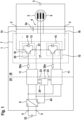
- Fig. 2 is a block diagram of the driver unit 11, being representative for any driver unit 11 connected to one of the switching elements 13, 15 of a respective half bridge 12.
- the driver unit 11 connected to the switching element 13 is described in detail, wherein all statements refer analogously to driver units 11 connected to the other switching elements 13, 15.
- the driver unit 11 comprises a first input terminal 27 for obtaining the supply voltage from the DC conversion unit 9 and a second input terminal 28 for obtaining the control signal 23 from the control unit 10. Furthermore, the driver unit 11 comprises a first output terminal 29 for connecting the control terminal 20 of the switching element 13 via a series resistor 20a. Moreover, the driver unit 11 comprises a second output terminal 30 for connecting the further terminal 21 of the switching element 13. Besides, the driver unit 11 comprises an output stage section 31, a first DC conversion section 32, a second DC conversion section 33 and an insulation element 34.
- the output stage section 31 comprises a high-side terminal 35, a low-side terminal 36 and a third input terminal 37 for obtaining the control signal 23, a fourth input terminal 38 and an output terminal 39 connected to the first output terminal 29 of the driver unit 11.
- the output stage section 31 is controllable based on the control signal 23 to connect either the high-side terminal 35 or the low-side terminal 36 to the output terminal 39 being connected to the first output terminal 29 of the driver unit 11.
- the first DC conversion section 32 comprises an input terminal 40, over which an input voltage 41 drops, a first output terminal 42 connected to the high-side terminal 35, a second output terminal 43 connected to the low-side terminal 36 and a third output terminal 44 connected to the second output terminal 30 of the driver unit 11.
- the first DC conversion section 32 is configured to supply the output stage section 31. Therein, the first DC conversion section 32 converts the input voltage 41 into a positive first voltage 45 between the high-side terminal 35 and the second output terminal 30. Thus, the first voltage 45 is provided between the first output terminal 42 and the third output terminal 44. Furthermore, the first DC conversion section 32 converts the input voltage 41 into a positive second voltage 46 between the second output terminal 30 of the driver unit 11 and the low-side terminal 36. Thus, the second voltage 46 is provided between the third output terminal 44 and the second output 43.
- the first DC conversion section 32 is configured to provide the first voltage 45 and the second voltage 46 such that, when the value of the first voltage 45 is above a threshold value, to which the first voltage 45 is limited, the value of the second voltage 46 increases with an increase of the input voltage 41.
- the value of the input voltage 45 is equal or higher than the threshold value.
- the first voltage 45 corresponds substantially to the input voltage 41 and the second voltage 46 is substantially zero.
- the switching off speed of the switching element 13 is varied as a high negative voltage discharges a capacity of the control terminal 20, i.e. a gate capacity of the power transistor 18, faster than a lower negative voltage.
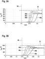
- Fig. 3A and 3B are diagrams of voltages 48a, 48, 48c, 48d over the switching path of the switching elements 13 over time t.
- Fig. 3A refers to the switching element 13 being an insulated gate bipolar transistor, so that the voltages 48a, 48b, 48c, 48d are collector-emitter-voltages (v CE ).
- Fig. 3B refers to the switching element 13 being an insulated gate field-effect transistor, so that the voltages 48a, 48b, 48c, 48d are drain-source-voltages (v DS ).
- a respective voltage 48a refers to a second voltage 46 of 0 V
- a respective voltage 48b refers to a second voltage 46 of 5 V
- a respective voltage 48c to a second voltage 46 of 10 V
- a respective voltage 48d to a second voltage 46 of 15 V for an exemplary configuration.
- the voltages 48a, 48b, 48c, 48d raise earlier on the cost of a higher voltage overshoot.
- the switching off speed of the switching element 13 is varied as a high negative voltage discharges a capacity of the controller terminal 12, i.e. a gate capacity of the power transistor 18, faster than a lower negative voltage.
- the maximum value of the voltages 48a to 48d is limited to a maximum rated blocking voltage 51.
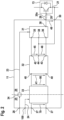
- Fig. 4 is a schematic diagram of the output stage section 31.
- the output stage section 31 comprises a push-pull-subsection 52, two resistors 53, 54 and an active subsection 55.
- the push-pull-subsection 52 comprises a controllable high-side switch 56 and a controllable low-side switch 57 being realized by two transistors of different types.
- the high-side switch 56 is realized by an npn-transistor and the low-side switch 57 is realized by a pnp-transistor.
- the low-side switch 56 is realized by an n-channel transistor and the high-side switch 57 is realized by a p-channel transistor.
- a central tap 58 between the switches 56, 57 is connected to the output terminal 39 of the output stage section 31.
- the resistor 53 is connected between the high-side terminal 35 and the high-side switch 56 of the push-pull-subsection 52, whereas the resistor 54 is connected between the low-side terminal 36 and the low-side switch 57.
- the push-pull-subsection 52 comprises a control terminal 59 connected to a respective control terminal of the switches 56, 57 via a series resistor 59a.
- the high-side switch 56 closes and the low-side switch 57 opens.
- the first voltage 45 drops between the resistor 53, the first output terminal 29 and the second output terminal 30, therein charging the capacity of the control terminal 20 of the switching element 13 with a positive voltage.
- the low-side switch 57 closes and the high-side switch 56 opens.
- the second voltage 46 drops between the second output terminal 30, the first output terminal 29 and the resistor 54, therein discharging the capacity of the control terminal 20 of the switching element 13 with a negative voltage.
- the active subsection 55 is used to increase the switching off speed with an increase of the second voltage 46.
- the active subsection 55 is connected in parallel to the resistor 54 between the first output terminal 39 and the low-side terminal 36 and is configured to sink a current increasing corresponding to an increase of the second voltage 46.
- the active subsection 55 comprises a reference value element 60 and an amplifier circuit 61, wherein the amplifier circuit 61 is configured to sink the current in addition to the current flowing through the resistor 54, when the value of second voltage exceeds a reference voltage provided by the reference value element 60. Therein, the amplifier circuit 61 switches a resistor 66a being part of the amplifier circuit in parallel to the resistor 54.
- the reference value element 60 is connected between the fourth input terminal 38 being connected to the second output terminal 30 of the driver unit 11 and the low-side terminal 36.
- the reference value element 60 comprises a Zener diode 62 and a resistor 63 connected in series, wherein central tap 64 therebetween is connected to an input 65 of the amplifier circuit 61.
- the amplifier circuit 61 may be realized by a transistor circuit 66 or an operational amplifier circuit, alternatively.
- the Zener voltage of the Zener diode 62 defines the reference voltage, which is chosen below the absolute value of a maximum rated negative voltage between the control terminal 20 and the further terminal 21 of the switching element 13. Thus, if the discharging current flowing through the resistor 54 does not result in the desired switching off speed, the switching off speed can be increased by the active subsection 55. Therein, the reference voltage is chosen such that at the maximum rated negative voltage the desired current being the sum of the current flowing through the resistor 54 and through the amplifier circuit 61 is achieved.
- Fig. 5 is a schematic diagram of the first DC conversion section 32.
- the first DC conversion section 32 comprises a push-pull-subsection 67, a reference value subsection 68 and two buffer capacitors 69, 70.
- the push-pull-subsection 67 comprises a high-side transistor 71, a low-side transistor 72 and a series resistor 73 connected between a control terminal 74 of the push-pull-subsection and a respective control terminal of the transistors 71, 72.
- the transistors 71, 72 are arranged between both potentials of the input voltage 41.
- a central tap 74a between the transistors 71, 72 is connected to the third output terminal 44 and via that to the second output terminal 30 of the driver unit 11 and the fourth input terminal 38 of the output stage section 31.
- the reference value subsection 68 comprises a Zener diode 75 and a resistor 76 connected in series. A central tap 77 therebetween is connected to the control terminal 74 of the push-pull-subsection 67. By means of the Zener diode 75 the threshold is defined.
- a voltage drop over the Zener diode 75 remains substantially constant, whereas a voltage drop over the resistor 76 increases.
- the voltage drop over the low-side transistor 72 increases, which provides the variable second voltage 46, whereas a voltage drop over the transistor 71, which corresponds to the first voltage 45 remains substantially constant.
- the buffer capacitor 69 connected between the first output terminal 42 and the third output terminal 45 buffers the first voltage 45.
- the buffer capacitor 70 connected between the thought output terminal 44 and the second output terminal 43 buffers the second voltage.
- the first DC conversion section 32 defines a reference potential at the third output terminal 44 for the further terminal 21 of the switching element 13 and provides in the normal operation, in which the first voltage 41 is above the threshold defined by the reference value subsection 68, the substantially constant first voltage 45 for switching on the switching element 13 and the variable second voltage 46 for switching off the switching element 13. Therein, the sum of the first voltage 45 and the second voltage 46 is equal to the input voltage 41.
- varying the input voltage 41 allows a corresponding variation of the switching off speed of the switching element 13.
- Fig. 6 is a schematic diagram of the second DC conversion section 33, which is realized by a resonant converter, here by an LLC converter.
- the second DC conversion section 33 comprises an input terminal 78, which obtains the supply voltage provided by conversion unit 9 as an input voltage 79 of the second DC conversion section 33 via the first input terminal 27. Furthermore, the second DC conversion section 33 comprises a switching subsection 80, a resonant circuit subsection 81, a transformer subsection 82, a rectifier subsection 83, a smoothing subsection 84 and an output terminal 85, at which an output voltage 86 being the input voltage 41 of the first DC conversion 32 is provided.
- the switching subsection 80 comprises a high-side switch 87 and a low-side switch 88, which each comprise a transistor 89 and a diode 90 connected in parallel.
- the transistor 89 may be an insulated gate bipolar transistor or an insulated gate field-effect transistor, wherein the last case the diode 90 is realized by the body diode of the transistor 89.
- the input voltage 79 is switched into an AC voltage for the further conversion by the resonant converter.
- the resonant circuit subsection 81 defines a resonance frequency of the resonant converter and is connected in parallel to the low-side switch 88 and to the transformer subsection 82.
- the resonant circuit subsection 81 comprises a capacitor 91 and a coil 92 connected in series and a magnetization inductance 93 in parallel to the transformer subsection 82.
- the coil 92 and the magnetization inductance 93 may by omitted so that the resonance frequency is defined by the capacitor 91 and an inductance of the transformer subsection 82.
- the resonant circuit subsection 81 may be of higher order, therein defining a plurality of resonant frequencies.
- the transformer subsection 82 decouples galvanically the first input terminal 27 on the one hand and the output terminals 29, 30, the output stage section 31 and the first DC conversion section 32 on the other hand.
- the primary side 25 and the secondary side 26 are considered as respective sides of the driver unit 11, the second DC conversion section 33 and the transformer section 82 as well.
- the galvanic decoupling is completed by the insulation element 34 (see Fig. 2 ) with respect to the control signal 23.
- the transformer subsection 82 transforms a voltage on the primary side 25 of the transformer subsection 82 into a voltage on the secondary 26 side of the transformer subsection 82, which is rectified to the DC output voltage 86 by means of the rectifier subsection 83, being a full bridge rectifier formed by four diodes 94, and smoothed by the smoothing subsection 84, comprising a capacitor 95.
- the rectifier subsection 83 may alternatively comprise a center tap topology, a voltage doubler topology or another commonly known topology.
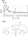
- Fig. 7 is a diagram of output voltage conversion ratios (V out /V in ) 96a, 96b, 96c, 96d, 96e over a normalized switching frequency (f s /f s0 ).
- the output voltage conversion ratio refers to the ratio of the output voltage 86 to the input voltage 79 and the normalized switching frequency to the ratio of a switching frequency of the switching subsection 80 to the resonance frequency of the series resonant circuit formed by the capacitor 91 and the coil 92.
- the ratio 96e refers to Q L converging toward infinity.
- the driver unit 11 is configured to control the switching subsection 18 to operate within an interval of e.g. 0.95 to 1.05 of the normalized switching frequency, preferably with a switching frequency substantially equal to the resonant frequency.
- the input voltage 79 is galvanically decoupled from the output voltage 86, which is a potential-free voltage being the input voltage 41 of the first DC conversion section 32.
- the switching off speed of the switching element 13 is controlled by the input voltage 79, which is provided by the DC conversion unit 9 of the electric power converter 1. Consequently, the variation of the switching off speed is based on the control information 24 determined by the control unit 10 of the electric power converter 1 and provided to the DC conversion unit 9. Based on the control information 24 the DC conversion unit 9 varies the supply voltage, which is the input voltage 79 of the second DC conversion section 33.
- the electric power converter 1 is not divided into the primary side 25 and the secondary side 26, wherein the second DC conversion section 33 is omitted and the input voltage 41 for the first DC conversion section is obtained directly at the first input terminal 27 of the driver unit 11.
- control information 24 is provided to the second DC conversion section 33 instead of being provided to the DC conversion unit 9, which is illustrated by dashed lines in Fig. 1 , 2 and 6 .
- the switching frequency of the switching subsection 80 is varied below the resonance frequency within a load-dependent operating area marked with reference sign 98 in Fig. 7 .
- a constant input voltage 79 is provided to the second DC conversion section and the output voltage 86 is varied by varying the switching frequency, which allows a corresponding variation of the switching off speed of the switching element 13.
- the control unit 10 is configured to determine the control information 24 based on the load of the second DC conversion 33 section, additionally.
- the second DC conversion section 33 comprises a further input terminal 99 (see Fig. 6 ) connected to the switching subsection 80 and the driver unit 11 comprises a further input terminal 100 (see Fig. 2 ) connected to the second DC conversion section 33.
- the control information 24 is obtained on the primary side 25 of the driver unit 11, therein avoiding a transmission of the control information 24 to the secondary side 26. Thus, an insulation element for transmitting the control information 24 is not required.
- the DC conversion unit 9 is omitted and the driver unit 11 are directly supplied by the voltage provided to the low-voltage terminal 8.
- the electric power converter 1 is a DC/DC converter, e.g. comprising a boost converter, a buck converter, a combined boost-buck-converter, a flyback converter, a phase-shifted full-bridge, a capacitive half bridge or another hard-switched half bridge.
- a DC/DC converter e.g. comprising a boost converter, a buck converter, a combined boost-buck-converter, a flyback converter, a phase-shifted full-bridge, a capacitive half bridge or another hard-switched half bridge.
- one or more switching elements of the DC/DC converter are connected to the driver unit 11 and the control unit 10 is configured to control the switching element such that the DC voltage provided to the DC link 2 is converted into a DC voltage by means of an additional inductance element.
- the electric power converter 1 is a controlled AC/DC converter such as a charging device for a battery.
- one or more switching elements of the AC/DC converter are connected to the driver unit 11 and the control unit 10 is configured to control the switching elements such that a AC voltage is rectified into a DC voltage.
- Fig. 8 is a block diagram of an embodiment of a vehicle 101 comprising an electric machine 5 for driving the vehicle, a high-voltage battery 3 and a low-voltage battery 22 and an electric power converter 1.
- the electric power converter 1 is configured to convert a DC voltage provided by the high-voltage battery 3 into an AC current supplying the electric machine 5, wherein the low-voltage battery 22 provides a supply voltage to the electric power converter 1.
- the vehicle 101 comprises an electric power converter 1 being a DC/DC converter for a wiring system (not shown) of the vehicle 101.
- the vehicle 101 comprises an electric power converter 1 being a AC/DC converter configured as an onboard charger for charging the high-voltage battery 3 by an AC voltage provided by a power grid.
Description
- The present invention relates to a driver unit for a voltage-controlled switching element according to the preamble of
claim 1. Aside, the invention relates to an electric power converter, a vehicle and a method for operating an electric power converter. - Driver units are widely known for providing a suitable power for charging and discharging a control terminal of a voltage-controlled switching element of an electric power converter based on a control signal, typically obtained from a control unit of the electric power converter. The driver unit comprises a first output terminal for connecting a control terminal of the switching element, such as a gate terminal, and a second output terminal for connecting a further terminal of the switching element, such as an emitter or a source terminal. Depending on the state of the control signal an output stage section connects its high-side terminal to the first output terminal for switching on the switching element or its low-side terminal to the first output terminal for switching off the switching element. A DC conversion section provides a positive first voltage between the high-side terminal and the second output terminal and a positive voltage between the second output terminal and the low-side terminal. Thus, between the first output terminal and the second output terminal a positive voltage drops, when the switching element is switched on, and a negative voltage drops, when the switching element is switched off.
- When switching off an ohmic-inductive load by the switching element, high transient voltages (du/dt) and currents (di/dt) occur that might damage the switching element. Particularly, the transient voltages can exceed a maximum rated voltage of the switching element due to parasitic of a commutation cell. The overshoot of the transient voltages can be influenced by a switching speed of the switching element. Therein, a slow switching off speed results in low transient voltages at the cost of high switching losses. Contrarily, a fast switching off speed causes high transient voltages but only low switching losses. Thus, it is desired to operate the switching element with an optimum switching off speed, which depends especially on an actual temperature of the switching element, a voltage to be switched, such as a voltage provided by a high-voltage battery of a vehicle, and an actual current of the ohmic-inductive.
- It has already been proposed to use an output stage section with two resistors connected controllably in parallel, through which a current flows from the first output terminal to the low-side terminal, when switching off the switching element. Therein, the current flows through one resistor for a slow switching off speed and through both resistors for a fast switching off speed. The resistors are controlled to be connected in parallel, if an additional control information representative for the switching off speed is received from the control unit.
- However, such a multiple resistor configuration allows only an inaccurate, stepwise adjustment of the switching off speed. Furthermore, large mounting space and additional components are required, particularly when more than two switching off speeds have to be realized by means of a corresponding number of resistors. Furthermore, the control information has to be transmitted to the output stage section, which requires additional wiring effort. Particularly, if the control unit has to be decoupled galvanically from the output stage section, the control information has to be transmitted over an insulation barrier by means of an insulation element, such as an optocoupler.
- Thus, it is an object of the invention to provide an improved driver unit, particularly allowing an accurate variation of the switching off speed and requiring less mounting space and less wiring and/or insulation effort.
- The above object is solved by a driver unit according to
claim 1. - The invention is based on the consideration to vary a switching off speed of the switching element by varying the second voltage provided between the second output terminal and the low-side terminal. Thus, if the second voltage increases, the absolute value of a negative voltage dropping between the first output terminal and the second output terminal of the driver unit increases as well. When switching off the switching element, a higher second voltage results in a higher discharge current of a capacity of the control terminal of the switching element and, consequently, in a faster switching off speed an in a faster di/dt. The variation of the second voltage and thus the variation of the switching off speed can be specified by a corresponding variation of the input voltage of the DC conversion section, when the first voltage is above the threshold value, which is a desired operation condition of the driver unit.
- Advantageously, the switching off speed can be varied independently of, i.e. additionally to, a variation of a resistance between the first output terminal of the driver unit and the low-side terminal of the output stage section. Therein, the switching off speed can be varied as accurate as the input voltage of the DC conversion section is variable. Furthermore, a transmission of a control information representative of the switching off speed to the output state section can be omitted. Consequently, less wiring effort is required.
- Typically, the switching element is a semiconductor switching element. The voltage-controlled switching element may comprise a power transistor, such as an insulated gate field-effect transistor or an insulated gate bipolar transistor. The switching element may further comprise a diode connected in parallel to the transistor. In the case of the transistor being an insulated gate field-effect transistor, the diode may be formed by a body diode of the transistor. The output stage section may have an output terminal connected to the first output terminal of the driver unit. The output stage section may have a resistor, which defines the switching on speed together with the first voltage, connected between the high-side terminal and the output terminal of the output stage section.
- The DC conversion section may have a first output terminal connected to the high-side terminal and/or a second output terminal connected to the low-side terminal and/or a third output terminal connected to the second output terminal. Typically, the first voltage drops between the first output terminal of the output stage section and the third output terminal of the output stage section and/or the second voltage drops between the third output terminal of the output stage section and the second output terminal of the output stage section. The output stage section may be configured such that the input voltage drops between its first output terminal and its second output terminal. Preferably, the DC conversion section is configured to provide the first voltage with a value between 10 V and 30 V and/or the second voltage with a value between 0 V and 20 V. The DC conversion section may comprise a buffer capacitor connected between its first output terminal and its third output terminal and/or a buffer capacitor connected between its second output terminal and its third output terminal.
- In general, it is possible that the DC conversion section is configured to provide the first voltage such that the first voltage increases slightly with an increase of the input voltage when being above the threshold value. However, it is preferred that the threshold value is a value, to which the first voltage is limited by the DC conversion section. This is because overvoltages typically do not occur when switching on the switching element, so that a variation of the switching on speed by means of varying the first voltage is not necessary. Furthermore, during an on-state of the switching element a constant control voltage is desirable in order to obtain steady conduction losses. Thus, the first voltage may be, particularly substantially, constant above the threshold value. The DC conversion section may be configured to convert the input voltage having a value below the threshold value into the first voltage, wherein the second voltage is, particularly substantially, zero. Alternatively or additionally, the DC conversion section may be configured to convert the input voltage having a value above the threshold value into the first voltage having a value corresponding to the threshold value and/or into the second voltage being the difference between the input voltage and the first voltage.
- Desirably, the DC conversion section comprises a push-pull-subsection having a central tap connected to the second output terminal of the driver unit. Thereby, it is assured that the central tap and the further terminal of the switching element are on the same potential. Typically, the push-pull-section comprises two transistors, particularly transistors of different types, such as an npn-transistor and a pnp-transistor or an n-channel transistor and a p-channel transistor, connected in series between both potentials of the input voltage.
- Furthermore, the DC conversion section may comprise a reference value subsection configured to define the threshold value and connected between a positive potential of the input voltage and a control terminal of the push-pull-subsection. The reference value subsection may comprise a Zener diode connected between the positive potential and the control terminal, which is preferably a common node of control terminals of the transistors of the push-pull-subsection. The Zener diode may be connected in series to a resistor. The resistor may be connected to the negative potential of the input voltage and the control terminal. Thus, the threshold value may be defined easily by the Zener voltage of the Zener diode.
- According to the invention, the output stage section comprises a push-pull-subsection having a central tap connected to the first output terminal of the driver unit. The output stage section may have a control terminal for obtaining the control signal. Therein, when the control signal is indicative for switching on the switching element, the high-side terminal may be connected to the first output terminal of the driver unit by the push-pull-subsection of the output stage section and, when the control signal is indicative for switching off the switching element, the low-side terminal may be connected to the first output terminal of the driver unit by the push-pull-subsection of the output stage section. Typically, the push-pull-section comprises two transistors, particularly transistors of different types, such as an npn-transistor and a pnp-transistor or an n-channel transistor and a p-channel transistor, connected in series.
- In general, the output stage section may comprise a resistor being interconnected between the first output terminal of the driver unit or the output terminal of the output stage section, respectively, and the low-side terminal. According to the invention, the output stage section comprises an active subsection interconnected between the first output terminal of the driver unit and the low-side terminal and configured to sink a current flowing to the low-side terminal increasing corresponding to an increase of the second voltage. Thereby, the switching off speed may be increased in comparison to the usage of only the resistor between the output terminal of the output stage section and the low-side terminal. Note that the current sunk by the active subsection depends on the variation of the input voltage, so that for the variation of the current a transmission of the control information representative for the switching off speed to the output stage section is avoided.
- The active subsection may comprise a reference value element and an amplifier circuit, wherein the amplifier circuit is configured to sink the current, when the value of second voltage exceeds a reference voltage provided by the reference value element. Typically, the reference value element is connected between the second output terminal of the driver unit and the low-side terminal. The reference value element may comprise a Zener diode and a resistor connected in series, wherein a central tap therebetween is connected to an input of the amplifier circuit. The amplifier circuit may comprise a transistor or an operational amplifier. Note that the amplifier circuit may be operated in a switching operation range or in an active operation range. Thus, the amplifier circuit being operated in the switching operation range may connect a resistor of the amplifier circuit in parallel to the resistor that is connected between the output terminal of the output stage section and the low-side terminal.
- For safety reasons it is preferred that the driver unit is divided into a primary side and a secondary side being decoupled galvanically from each other, wherein the DC conversion section and/or the output stage section and/or the output terminals of the driver unit are part of the secondary side and a first input terminal of the driver unit for providing a supply voltage for the driver unit and/or a second input terminal of the driver unit for obtaining the control signal and/or a third input terminal of the driver unit for obtaining a control information representative for a switching off speed of the switching element are part of the primary side. The second input terminal of the driver unit may be decoupled galvanically by means of an insulation element, particularly an optocoupler, an inductive insulation element or a capacitive insulation element, forming an interface between the primary side and the secondary side.
- Advantageously, the driver unit comprises a second DC conversion section configured to convert an input voltage into an output voltage provided to the first DC conversion section as its input voltage. Thus, the second DC conversion section may be used to provide the input voltage of the first DC conversion section with a desired value corresponding to the switching off speed as the input of the first DC conversion section. Typically, the input voltage of the second DC conversion section is obtained from the first input terminal of the driver unit. If the second DC conversion section is omitted, the input voltage of the first DC conversion section is obtained from the first input terminal of the driver unit.
- Moreover, the first input terminal of the driver unit on the one hand and the first DC conversion section, the output stage section and the output terminals of the driver unit on the other hand may be galvanically decoupled by the second DC conversion section.
- Preferably, the second DC conversion section comprises a resonant converter, particularly an LLC-converter. The second DC conversion section may comprise a transformer subsection, which decouples galvanically the first input terminal of the driver unit on the one hand and the first DC conversion section, the output stage section and the output terminals on the other hand. Particularly, on the primary side of the transformer subsection the resonant converter comprises a switching section and/or a resonant circuit subsection. On the secondary side of the transformer subsection the resonant converter may comprise a rectifier subsection configured to rectify a voltage transformed by the transformer subsection and preferably a smoothing capacitor subsection configured to smooth the rectified voltage.
- As a first alternative, the driver unit may be configured to control a switching subsection of the resonant converter with a switching frequency within an interval enclosing a resonance frequency of the resonant converter. This allows the input voltage to be transferred substantially independently of the load of the second DC conversion section. Typically, the interval is limited by 0.9 times the resonance frequency and by 1.1 times the resonance frequency.
- As a second alternative, the driver unit may be configured to control a switching subsection of the resonant converter with a switching frequency being below a resonance frequency of the resonant converter based on the control information representative for a switching off speed of the switching element. Thereby, the voltage conversion ratio and the switching off speed is varied corresponding to the switching frequency being in a load-dependent operating range of the resonant converter. Therein, the switching frequency may be determined based on a desired output voltage of the second DC conversion section.
- With respect to both alternatives, the switching subsection may comprise a plurality of switches being arranged in a half bridge or in a full bridge.
- Aside, the present invention refers to an electric power converter, comprising a driver unit according to the invention. The electric power converter is preferably an inverter. Alternatively, the electric power converter may be a DC/DC converter, particularly comprising a boost converter, a buck converter, a combined boost-buck-converter, a flyback converter, a phase-shifted full-bridge, a capacitive half bridge or another hard-switched half bridge. Furthermore, the electric power converter may be a, particularly controlled, AC/DC converter.
- The electric power converter may comprise a control unit configured to provide the control signal and/or the control information. Preferably, the control unit is configured to determine the switching frequency and to provide it by means of the control information to the driver unit.
- Moreover, the present invention refers to a vehicle comprising at least one electric power converter according to the invention. Therein, one electric power converter is configured to supply an electric machine of the vehicle and/or one electric power converter is a DC/DC converter in a wiring system of the vehicle and/or one electric power converter is an AC/DC converter being configured as an onboard charger for a high-voltage battery of the vehicle.
- Finally, the present invention refers to a method according to
claim 14. - All statements referring to the inventive driver unit apply analogously to the inventive electric power converter, the inventive vehicle and the inventive method, so that the above-mentioned advantages of the inventive driver unit may be achieved as well.
- Further details and advantages of the invention are disclosed in the following, wherein reference is made to the drawings showing:
- Fig. 1
- a block diagram of an embodiment of an electric power converter;
- Fig. 2
- a block diagram of a driver unit of the electric power converter depicted in
Fig. 1 ; - Fig. 3A, 3B
- diagrams of voltages across a switching path of the switching element over time;
- Fig. 4
- a schematic diagram of an output stage section of the driver unit depicted in
Fig. 2 ; - Fig. 5
- a schematic diagram of a first DC conversion section of the driver unit depicted in
Fig. 2 ; - Fig. 6
- a schematic diagram of a second DC conversion section of the driver unit depicted in
Fig. 2 ; - Fig. 7
- a diagram of output voltage conversion ratios of the second DC conversion section depicted in
Fig. 6 over a normalized switching frequency; and - Fig. 8
- a block diagram of an embodiment of a vehicle.
-
Fig. 1 is a block diagram of a first embodiment of anelectric power converter 1, which is exemplarily depicted as an inverter. Thus, aDC link 2 with anDC link capacitor 2a of theelectric power converter 1 is connected to a firstDC voltage source 3, which is e.g. a high-voltage battery having a nominal voltage of e. g. 500 V. An AC output 4 of theelectric power converter 1 is connected toelectric machine 5, wherein the AC output 4 provides a multi-phase AC current tostator windings 6 of theelectric machine 5. - Furthermore, the
electric power converter 1 comprises apower unit 7 connected between theDC link 2 and the AC output 4, a low-voltage input 8, a DC conversion unit 9, acontrol unit 10 anddriver units 11. - As the
electric power converter 1 is an inverter, thepower unit 7 comprises a plurality ofhalf bridges 12 connected in parallel to each other and to a smoothing capacitor (not shown) of theDC link 2. For each phase of the AC output 4 onehalf bridge 12 is provided. Eachhalf bridge 12 comprises a voltage-controlledswitching element 13 connected to ahigh potential 14 of theDC link 2 and a voltage-controlledswitching element 15 connected to alow potential 16 of theDC link 2. The switchingelements - Each switching
element power transistor 18 being an insulated gate bipolar transistor and adiode 19 connected in parallel. Alternatively, thepower transistor 18 is an insulated gate field-effect transistor, wherein thediode 19 may be formed by a body diode of the insulated gate field-effect transistor. Each switchingelement control terminal 20, which is formed by a gate terminal of thetransistor 18, and afurther terminal 21 connected to a switching path realized by the switchingelement element power transistor 18 thefurther terminal 21 is formed by an emitter terminal or a source terminal, respectively. - The low-voltage input 8 is connected to a
second DC source 22, which is e.g. a low-voltage battery having a nominal voltage of 12 V. Via the low-voltage input 8 an operating voltage for thecontrol unit 10 is provided, wherein a wiring therebetween is not shown inFig. 1 for reasons of simplicity. Furthermore, the low-voltage input 8 is connected to the DC conversion unit 9, being e.g. a buck converter or a boost converter, configured to provide a supply voltage to thedriver units 11. - The
control unit 10 is configured to provide acontrol signal 23 representative for switching arespective switching element control signal 23 represents a pulse-width-modulated switching pattern according to which arespective switching element half bridge 12 is switched on or off such that the multiphase AC current is provided at the AC output 4. - Furthermore, the
control unit 10 is configured to provide acontrol information 24 representative for a desired switching off speed of the switchingelements control unit 10 is configured to determine the switching off speed based on an actual temperature of the switchingelements DC link 2, an actual load current at the AC output 4 and an actual temperature of a coolant cooling theswitching elements elements elements - Furthermore, the
electric power converter 1 is divided into aprimary side 25 and asecondary side 26 being decoupled galvanically from each other, which is represented by a dot dashed line in the figures. Theprimary side 25 may be considered as a low-voltage side of theelectric power converter 1 and comprises the low-voltage input 8, the DC conversion unit 9 and thecontrol unit 10. Thesecondary side 26 may be considered as a high-voltage side of theelectric power converter 1 and comprises theDC link 2, the AC output 4 and thepower unit 7. Thedriver units 11 are an interface between theprimary side 25 and thesecondary side 26. -
Fig. 2 is a block diagram of thedriver unit 11, being representative for anydriver unit 11 connected to one of the switchingelements respective half bridge 12. In the following thedriver unit 11 connected to the switchingelement 13 is described in detail, wherein all statements refer analogously todriver units 11 connected to theother switching elements - The
driver unit 11 comprises afirst input terminal 27 for obtaining the supply voltage from the DC conversion unit 9 and a second input terminal 28 for obtaining thecontrol signal 23 from thecontrol unit 10. Furthermore, thedriver unit 11 comprises afirst output terminal 29 for connecting thecontrol terminal 20 of the switchingelement 13 via aseries resistor 20a. Moreover, thedriver unit 11 comprises asecond output terminal 30 for connecting thefurther terminal 21 of the switchingelement 13. Besides, thedriver unit 11 comprises anoutput stage section 31, a firstDC conversion section 32, a secondDC conversion section 33 and aninsulation element 34. - The
output stage section 31 comprises a high-side terminal 35, a low-side terminal 36 and athird input terminal 37 for obtaining thecontrol signal 23, afourth input terminal 38 and anoutput terminal 39 connected to thefirst output terminal 29 of thedriver unit 11. Theoutput stage section 31 is controllable based on thecontrol signal 23 to connect either the high-side terminal 35 or the low-side terminal 36 to theoutput terminal 39 being connected to thefirst output terminal 29 of thedriver unit 11. Therein, when thecontrol signal 23 is indicative for switching on the switchingelement 13, the high-side terminal 35 is connected to theoutput terminal 39 and, when thecontrol signal 23 is indicative for switching off the switchingelement 13, the low-side terminal 36 is connected to theoutput terminal 39. - The first
DC conversion section 32 comprises aninput terminal 40, over which aninput voltage 41 drops, afirst output terminal 42 connected to the high-side terminal 35, asecond output terminal 43 connected to the low-side terminal 36 and athird output terminal 44 connected to thesecond output terminal 30 of thedriver unit 11. The firstDC conversion section 32 is configured to supply theoutput stage section 31. Therein, the firstDC conversion section 32 converts theinput voltage 41 into a positivefirst voltage 45 between the high-side terminal 35 and thesecond output terminal 30. Thus, thefirst voltage 45 is provided between thefirst output terminal 42 and thethird output terminal 44. Furthermore, the firstDC conversion section 32 converts theinput voltage 41 into a positivesecond voltage 46 between thesecond output terminal 30 of thedriver unit 11 and the low-side terminal 36. Thus, thesecond voltage 46 is provided between thethird output terminal 44 and thesecond output 43. - Consequently, when the
control signal 23 is indicative for switching on the switchingelement 13, the positivefirst voltage 45 is used for switching on the switchingelement 13. When thecontrol signal 23 is indicative for switching off the switchingelement 13, the invertedsecond voltage 46, thus negative voltage, is used for switching off the switchingelement 13. - The first
DC conversion section 32 is configured to provide thefirst voltage 45 and thesecond voltage 46 such that, when the value of thefirst voltage 45 is above a threshold value, to which thefirst voltage 45 is limited, the value of thesecond voltage 46 increases with an increase of theinput voltage 41. Therein, in a normal operation of thedriver unit 11 the value of theinput voltage 45 is equal or higher than the threshold value. Thus, when theinput voltage 41 is equal to the threshold value, thefirst voltage 45 corresponds substantially to theinput voltage 41 and thesecond voltage 46 is substantially zero. Upon increasing theinput voltage 41, thefirst voltage 45 remains substantially constant and thesecond voltage 46 increases, which results in a more negative voltage for switching off the switchingelement 13. Thus, by varying theinput voltage 41 above the threshold value, the switching off speed of the switchingelement 13 is varied as a high negative voltage discharges a capacity of thecontrol terminal 20, i.e. a gate capacity of thepower transistor 18, faster than a lower negative voltage. -
Fig. 3A and 3B are diagrams ofvoltages elements 13 over time t.Fig. 3A refers to the switchingelement 13 being an insulated gate bipolar transistor, so that thevoltages Fig. 3B refers to the switchingelement 13 being an insulated gate field-effect transistor, so that thevoltages respective voltage 48a refers to asecond voltage 46 of 0 V, arespective voltage 48b refers to asecond voltage 46 of 5 V, arespective voltage 48c to asecond voltage 46 of 10 V and arespective voltage 48d to asecond voltage 46 of 15 V for an exemplary configuration. - As can be seen by increasing the second voltage 46 - corresponding to a decrease of a
voltage 49 between thefirst output terminal 29 and the second output terminal 30 - thevoltages input voltage 41 above the threshold voltage, the switching off speed of the switchingelement 13 is varied as a high negative voltage discharges a capacity of thecontroller terminal 12, i.e. a gate capacity of thepower transistor 18, faster than a lower negative voltage. Note that the maximum value of thevoltages 48a to 48d is limited to a maximum rated blockingvoltage 51. -
Fig. 4 is a schematic diagram of theoutput stage section 31. Theoutput stage section 31 comprises a push-pull-subsection 52, tworesistors active subsection 55. - The push-pull-
subsection 52 comprises a controllable high-side switch 56 and a controllable low-side switch 57 being realized by two transistors of different types. Therein, the high-side switch 56 is realized by an npn-transistor and the low-side switch 57 is realized by a pnp-transistor. Alternatively, the low-side switch 56 is realized by an n-channel transistor and the high-side switch 57 is realized by a p-channel transistor. Acentral tap 58 between theswitches output terminal 39 of theoutput stage section 31. Theresistor 53 is connected between the high-side terminal 35 and the high-side switch 56 of the push-pull-subsection 52, whereas theresistor 54 is connected between the low-side terminal 36 and the low-side switch 57. The push-pull-subsection 52 comprises acontrol terminal 59 connected to a respective control terminal of theswitches series resistor 59a. - Upon receiving the
control signal 23 being indicative for switching on the switchingelement 13 via thethird input terminal 37 at thecontrol terminal 59 of the push-pull-subsection 52 the high-side switch 56 closes and the low-side switch 57 opens. Then thefirst voltage 45 drops between theresistor 53, thefirst output terminal 29 and thesecond output terminal 30, therein charging the capacity of thecontrol terminal 20 of the switchingelement 13 with a positive voltage. Upon receiving thecontrol signal 23 being indicative for switching off the switchingelement 13 at thecontrol terminal 59 the low-side switch 57 closes and the high-side switch 56 opens. Then thesecond voltage 46 drops between thesecond output terminal 30, thefirst output terminal 29 and theresistor 54, therein discharging the capacity of thecontrol terminal 20 of the switchingelement 13 with a negative voltage. - The
active subsection 55 is used to increase the switching off speed with an increase of thesecond voltage 46. Theactive subsection 55 is connected in parallel to theresistor 54 between thefirst output terminal 39 and the low-side terminal 36 and is configured to sink a current increasing corresponding to an increase of thesecond voltage 46. Theactive subsection 55 comprises areference value element 60 and anamplifier circuit 61, wherein theamplifier circuit 61 is configured to sink the current in addition to the current flowing through theresistor 54, when the value of second voltage exceeds a reference voltage provided by thereference value element 60. Therein, theamplifier circuit 61 switches aresistor 66a being part of the amplifier circuit in parallel to theresistor 54. - The
reference value element 60 is connected between thefourth input terminal 38 being connected to thesecond output terminal 30 of thedriver unit 11 and the low-side terminal 36. Thereference value element 60 comprises aZener diode 62 and aresistor 63 connected in series, whereincentral tap 64 therebetween is connected to aninput 65 of theamplifier circuit 61. Theamplifier circuit 61 may be realized by atransistor circuit 66 or an operational amplifier circuit, alternatively. - The Zener voltage of the
Zener diode 62 defines the reference voltage, which is chosen below the absolute value of a maximum rated negative voltage between thecontrol terminal 20 and thefurther terminal 21 of the switchingelement 13. Thus, if the discharging current flowing through theresistor 54 does not result in the desired switching off speed, the switching off speed can be increased by theactive subsection 55. Therein, the reference voltage is chosen such that at the maximum rated negative voltage the desired current being the sum of the current flowing through theresistor 54 and through theamplifier circuit 61 is achieved.Fig. 5 is a schematic diagram of the firstDC conversion section 32. The firstDC conversion section 32 comprises a push-pull-subsection 67, areference value subsection 68 and twobuffer capacitors - The push-pull-
subsection 67 comprises a high-side transistor 71, a low-side transistor 72 and aseries resistor 73 connected between acontrol terminal 74 of the push-pull-subsection and a respective control terminal of thetransistors transistors input voltage 41. Acentral tap 74a between thetransistors third output terminal 44 and via that to thesecond output terminal 30 of thedriver unit 11 and thefourth input terminal 38 of theoutput stage section 31. - The
reference value subsection 68 comprises aZener diode 75 and aresistor 76 connected in series. Acentral tap 77 therebetween is connected to thecontrol terminal 74 of the push-pull-subsection 67. By means of theZener diode 75 the threshold is defined. - Upon a variation of the
input voltage 41 being above the threshold a voltage drop over theZener diode 75 remains substantially constant, whereas a voltage drop over theresistor 76 increases. Thus, the voltage drop over the low-side transistor 72 increases, which provides the variablesecond voltage 46, whereas a voltage drop over thetransistor 71, which corresponds to thefirst voltage 45 remains substantially constant. Thebuffer capacitor 69 connected between thefirst output terminal 42 and thethird output terminal 45 buffers thefirst voltage 45. Thebuffer capacitor 70 connected between the thoughtoutput terminal 44 and thesecond output terminal 43 buffers the second voltage. - In sum, the first
DC conversion section 32 defines a reference potential at thethird output terminal 44 for thefurther terminal 21 of the switchingelement 13 and provides in the normal operation, in which thefirst voltage 41 is above the threshold defined by thereference value subsection 68, the substantially constantfirst voltage 45 for switching on the switchingelement 13 and the variablesecond voltage 46 for switching off the switchingelement 13. Therein, the sum of thefirst voltage 45 and thesecond voltage 46 is equal to theinput voltage 41. Thus, varying theinput voltage 41 allows a corresponding variation of the switching off speed of the switchingelement 13. -
Fig. 6 is a schematic diagram of the secondDC conversion section 33, which is realized by a resonant converter, here by an LLC converter. - The second
DC conversion section 33 comprises aninput terminal 78, which obtains the supply voltage provided by conversion unit 9 as aninput voltage 79 of the secondDC conversion section 33 via thefirst input terminal 27. Furthermore, the secondDC conversion section 33 comprises a switchingsubsection 80, aresonant circuit subsection 81, atransformer subsection 82, arectifier subsection 83, a smoothingsubsection 84 and anoutput terminal 85, at which anoutput voltage 86 being theinput voltage 41 of thefirst DC conversion 32 is provided. - The switching
subsection 80 comprises a high-side switch 87 and a low-side switch 88, which each comprise atransistor 89 and adiode 90 connected in parallel. Again, thetransistor 89 may be an insulated gate bipolar transistor or an insulated gate field-effect transistor, wherein the last case thediode 90 is realized by the body diode of thetransistor 89. By means of the switchingsubsection 80, theinput voltage 79 is switched into an AC voltage for the further conversion by the resonant converter. - The
resonant circuit subsection 81 defines a resonance frequency of the resonant converter and is connected in parallel to the low-side switch 88 and to thetransformer subsection 82. Theresonant circuit subsection 81 comprises acapacitor 91 and acoil 92 connected in series and amagnetization inductance 93 in parallel to thetransformer subsection 82. Thecoil 92 and themagnetization inductance 93 may by omitted so that the resonance frequency is defined by thecapacitor 91 and an inductance of thetransformer subsection 82. Alternatively, theresonant circuit subsection 81 may be of higher order, therein defining a plurality of resonant frequencies. - The
transformer subsection 82 decouples galvanically thefirst input terminal 27 on the one hand and theoutput terminals output stage section 31 and the firstDC conversion section 32 on the other hand. Thus, theprimary side 25 and thesecondary side 26 are considered as respective sides of thedriver unit 11, the secondDC conversion section 33 and thetransformer section 82 as well. The galvanic decoupling is completed by the insulation element 34 (seeFig. 2 ) with respect to thecontrol signal 23. - The
transformer subsection 82 transforms a voltage on theprimary side 25 of thetransformer subsection 82 into a voltage on the secondary 26 side of thetransformer subsection 82, which is rectified to theDC output voltage 86 by means of therectifier subsection 83, being a full bridge rectifier formed by fourdiodes 94, and smoothed by the smoothingsubsection 84, comprising acapacitor 95. Note that the a full bridge rectifier is described here exemplarily and that therectifier subsection 83 may alternatively comprise a center tap topology, a voltage doubler topology or another commonly known topology. -
Fig. 7 is a diagram of output voltage conversion ratios (Vout/Vin) 96a, 96b, 96c, 96d, 96e over a normalized switching frequency (fs/fs0). Therein, the output voltage conversion ratio refers to the ratio of theoutput voltage 86 to theinput voltage 79 and the normalized switching frequency to the ratio of a switching frequency of the switchingsubsection 80 to the resonance frequency of the series resonant circuit formed by thecapacitor 91 and thecoil 92. Thevoltage conversion ratios 96a to 96e refer to different normalized loads QL being the ratio of an ohmic load of the resonant converter to a significant impedance
coil 92 and C denotes the capacitance of thecapacitor 91. Therein, theratio 96a refers to QL = 0.1, theratio 96b refers to QL = 1, the ratio 96c refers to QL = 5, the ratio 96d refers to QL = 10 and the ratio 96e refers to QL converging toward infinity. - As can be seen from
Fig. 7 , by controlling the switchingsubsection 80 to switch within an interval near fs/fs0 = 1 the outputvoltage conversion ratios 96a to 96e are substantially independent of the load. An operating area around a load-independent operating point is marked withreference sign 97. Thus, thedriver unit 11 is configured to control the switchingsubsection 18 to operate within an interval of e.g. 0.95 to 1.05 of the normalized switching frequency, preferably with a switching frequency substantially equal to the resonant frequency. - Therein, the
input voltage 79 is galvanically decoupled from theoutput voltage 86, which is a potential-free voltage being theinput voltage 41 of the firstDC conversion section 32. The switching off speed of the switchingelement 13 is controlled by theinput voltage 79, which is provided by the DC conversion unit 9 of theelectric power converter 1. Consequently, the variation of the switching off speed is based on thecontrol information 24 determined by thecontrol unit 10 of theelectric power converter 1 and provided to the DC conversion unit 9. Based on thecontrol information 24 the DC conversion unit 9 varies the supply voltage, which is theinput voltage 79 of the secondDC conversion section 33. - According to a further embodiment corresponding to the first embodiment, the
electric power converter 1 is not divided into theprimary side 25 and thesecondary side 26, wherein the secondDC conversion section 33 is omitted and theinput voltage 41 for the first DC conversion section is obtained directly at thefirst input terminal 27 of thedriver unit 11. - According to a further embodiment corresponding to the first embodiment of the
electric power converter 1, thecontrol information 24 is provided to the secondDC conversion section 33 instead of being provided to the DC conversion unit 9, which is illustrated by dashed lines inFig. 1 ,2 and6 . - Therein, by means of the
control information 24 the switching frequency of the switchingsubsection 80 is varied below the resonance frequency within a load-dependent operating area marked withreference sign 98 inFig. 7 . As can be seen in this operating area the output voltage conversion ratio highly depends on the switching frequency within an interval of the normalized switching frequency limited by fs/fs0 = 0.4 and fs/fs0 = 0.6. Thus, according to the present embodiment aconstant input voltage 79 is provided to the second DC conversion section and theoutput voltage 86 is varied by varying the switching frequency, which allows a corresponding variation of the switching off speed of the switchingelement 13. Within the operatingarea 98 the output voltage ratio depends on the load of the secondDC conversion section 33. Accordingly, thecontrol unit 10 is configured to determine thecontrol information 24 based on the load of thesecond DC conversion 33 section, additionally. - For obtaining the
control information 24 the secondDC conversion section 33 comprises a further input terminal 99 (seeFig. 6 ) connected to the switchingsubsection 80 and thedriver unit 11 comprises a further input terminal 100 (seeFig. 2 ) connected to the secondDC conversion section 33. Note that thecontrol information 24 is obtained on theprimary side 25 of thedriver unit 11, therein avoiding a transmission of thecontrol information 24 to thesecondary side 26. Thus, an insulation element for transmitting thecontrol information 24 is not required. - According to a further embodiment of the
electric power converter 1 corresponding to the aforementioned one, the DC conversion unit 9 is omitted and thedriver unit 11 are directly supplied by the voltage provided to the low-voltage terminal 8. - According to a further embodiment corresponding to the aforementioned ones, the
electric power converter 1 is a DC/DC converter, e.g. comprising a boost converter, a buck converter, a combined boost-buck-converter, a flyback converter, a phase-shifted full-bridge, a capacitive half bridge or another hard-switched half bridge. Therein, one or more switching elements of the DC/DC converter are connected to thedriver unit 11 and thecontrol unit 10 is configured to control the switching element such that the DC voltage provided to theDC link 2 is converted into a DC voltage by means of an additional inductance element. - According to a further embodiment, the
electric power converter 1 is a controlled AC/DC converter such as a charging device for a battery. Therein, one or more switching elements of the AC/DC converter are connected to thedriver unit 11 and thecontrol unit 10 is configured to control the switching elements such that a AC voltage is rectified into a DC voltage. -
Fig. 8 is a block diagram of an embodiment of avehicle 101 comprising anelectric machine 5 for driving the vehicle, a high-voltage battery 3 and a low-voltage battery 22 and anelectric power converter 1. Therein, theelectric power converter 1 is configured to convert a DC voltage provided by the high-voltage battery 3 into an AC current supplying theelectric machine 5, wherein the low-voltage battery 22 provides a supply voltage to theelectric power converter 1. Aside, thevehicle 101 comprises anelectric power converter 1 being a DC/DC converter for a wiring system (not shown) of thevehicle 101. Furthermore, thevehicle 101 comprises anelectric power converter 1 being a AC/DC converter configured as an onboard charger for charging the high-voltage battery 3 by an AC voltage provided by a power grid.
Claims (14)
- Driver unit (11) for a voltage-controlled switching element (13), comprising- a first output terminal (29) for connecting a control terminal (20) of the switching element (13),- a second output terminal (30) for connecting a further terminal (21) of the switching element (13),- an output stage section (31) having an output terminal (38, 39) connected to the first output terminal (29) of the driver unit (11), a high-side terminal (35) and a low-side terminal (36) and being controllable to connect one of its high-side terminal (35) or low-side terminal (36) to the first output terminal (29) of the driver unit (11) based on a control signal (23) representative for switching the switching element (13), wherein, when the control signal (23) is indicative for switching on the switching element (13), the high-side terminal (35) is connected to the output terminal (39) of the output stage section (31) and, when the control signal (23) is indicative for switching off the switching element (13), the low-side terminal (36) is connected to the output terminal (39) of the output stage section (31) and- a DC conversion section (32) configured to supply the output stage section (31) and to convert an input voltage (41) into a positive first voltage (45) between the high-side terminal (35) and the second output terminal (30) of the driver unit (11) and into a positive second voltage (46) between the second output terminal (30) of the driver unit (11) and the low-side terminal (36),characterized in thatthe DC conversion section (32) is configured to provide the first voltage (45) andthe second voltage (46) such that, when a value of the first voltage (45) is above a threshold value, with an increase of the input voltage (41) a value of the second voltage (46) is configured to increase more than the first voltage (45), whereinthe output stage section (31) comprises a push-pull-subsection (52) having a central tap (58) connected to the first output terminal (29) of the driver unit (11),wherein the output stage section (31) further comprises an active subsection (55) interconnected between the first output terminal (29) of the driver unit (11) and the low-side terminal (36) and configured to sink a current flowing to the low-side terminal (36) increasing corresponding to an increase of the second voltage (46).
- Driver unit according to claim 1, wherein the threshold value is a value, to which the first voltage (45) is limited by the DC conversion section (32).
- Driver unit according to claim 1 or 2, wherein the DC conversion section (32) comprises a push-pull-subsection (67) having a central tap (74a) connected to the second output terminal (30) of the driver unit (11).
- Driver unit according to claim 3, wherein the DC conversion section (32) comprises a reference value subsection (68) configured to define the threshold value and connected between a positive potential of the input voltage (41) and a control terminal (74) of the push-pull-subsection (67).
- Driver unit according to any of the preceding claims, wherein the push-pull-subsection (52) has a control terminal (59) for obtaining the control signal (23).
- Driver unit according to any of the preceding claims, wherein the active subsection (55) comprises a reference value element (60) and an amplifier circuit (61), wherein the amplifier circuit (61) is configured to sink the current, when the value of second voltage (46) exceeds a reference voltage provided by the reference value element (60).
- Driver unit according to any of the preceding claims, wherein the driver unit (11) is divided into a primary side (25) and a secondary side (26) being decoupled galvanically form each other, wherein the DC conversion section and/or the output stage section (31) and/or the output terminals (29, 30) of the driver unit (11) are part of the secondary side (25) and a first input terminal (27) of the driver unit (11) for providing a supply voltage for the driver unit (11) and/or a second input terminal (28) of the driver unit (11) for obtaining the control signal (23) and/or a third input terminal (100) of the driver unit (11) for obtaining a control information (24) representative for a switching off speed of the switching element (13) are part of the primary side (25).
- Driver unit according to any of the preceding claims, wherein the driver unit (11) comprises a second DC conversion section (33) configured to convert an input voltage (79) into an output voltage (86) provided to the first DC conversion section (32) as its input voltage (41).
- Driver unit according to claim 7 and 8, wherein the first input terminal (27) on the one hand and the first DC conversion section (32), the output stage section (31) and the output terminals (29, 30) of the driver unit (11) on the other hand are galvanically decoupled by the second DC conversion section (33).
- Driver unit according to claim 8 or 9, wherein the second DC conversion (33) section comprises a resonant converter, particularly an LLC-converter.
- Driver unit according to claim 10, wherein the driver unit (11) is configured to control a switching subsection (80) of the resonant converter with a switching frequency within an interval enclosing a resonance frequency of the resonant converter or to control a switching subsection (80) of the resonant converter with a switching frequency being below a resonance frequency of the resonant converter based on the or a control information (24) representative for a switching off speed of the switching element (13).
- Electric power converter (1), particularly an inverter or a DC/DC converter or an AC/DC converter, comprising a driver unit (11) according to any of claims 1 to 11.
- Vehicle (101), comprising at least one electric power converter (1) according to claim 12, wherein one electric power converter (1) is configured to supply an electric machine (5) of the vehicle (101) and/or one electric power converter (1) is a DC/DC converter in a wiring system of the vehicle (101) and/or one electric power converter (1) is an AC/DC converter being configured as an onboard charger for a high-voltage battery (3) of the vehicle (5).
- Method for operating an electric power converter (1) having a voltage-controlled switching element (13) and a driver unit (11), wherein the driver unit comprises- a first output terminal (29) connected to a control terminal (20) of the switching element (13),- a second output terminal (30) connected to a further terminal (21) of the switching element (13),- an output stage section (31) having an output terminal (39) connected to the first output terminal of the driver unit (11), a high-side terminal (35) and a low-side terminal (36) and being controlled to connect one of its terminals (35, 36) to the first output terminal (29) of the driver unit (11) based on a control signal (23) representative for switching the switching element (13), wherein, when the control signal (23) is indicative for switching on the switching element (13), the high-side terminal (35) is connected to the output terminal (39) of the output stage section (31) and, when the control signal (23) is indicative for switching off the switching element (13), the low-side terminal is connected to the output terminal (39) of the output stage section (31), wherein the output stage section (31) comprises a push-pull-subsection (52) having a central tap (58) connected to the first output terminal (29) of the driver unit (11), wherein the output stage section (31) further comprises an active subsection (55) interconnected between the first output terminal (29) of the driver unit (11) and the low-side terminal (36), and- a DC conversion section (32),wherein the DC conversion section (32) supplies the output stage section (31) and converts an input voltage (41) into a positive first voltage (45) between the high-side terminal (35) and the second output terminal (30) of the driver unit (11) and into a positive second voltage (46) between the second output terminal (30) of the driver unit (11) and the low-side terminal (36), wherein the DC conversion section (32) provides the first voltage (45) and the second voltage (46) such that, when a value of the first voltage (45) is above a threshold value, with an increase of the input voltage (41) a value of the second voltage (46) increases more than the first voltage (45), wherein the active subsection (55) sinks a current flowing to the low-side terminal (36) increasing corresponding to an increase of the second voltage (46).
Priority Applications (5)
| Application Number | Priority Date | Filing Date | Title |
|---|---|---|---|
| HUE17210343A HUE052197T2 (en) | 2017-12-22 | 2017-12-22 | Driver unit, electric power converter, vehicle and method for operating an electric power converter |
| EP17210343.4A EP3503364B2 (en) | 2017-12-22 | 2017-12-22 | Driver unit, electric power converter, vehicle and method for operating an electric power converter |
| US16/217,849 US10917000B2 (en) | 2017-12-22 | 2018-12-12 | Driver unit, electric power converter, vehicle and method for operating an electric power converter |
| CN201811558124.6A CN109962617A (en) | 2017-12-22 | 2018-12-19 | Actuator unit, vehicle, electric power converter and its operating method |
| JP2018238591A JP7436142B2 (en) | 2017-12-22 | 2018-12-20 | Drive units, electric power converters, vehicles, and methods of driving electric power converters |
Applications Claiming Priority (1)
| Application Number | Priority Date | Filing Date | Title |
|---|---|---|---|
| EP17210343.4A EP3503364B2 (en) | 2017-12-22 | 2017-12-22 | Driver unit, electric power converter, vehicle and method for operating an electric power converter |
Publications (3)
| Publication Number | Publication Date |
|---|---|
| EP3503364A1 EP3503364A1 (en) | 2019-06-26 |
| EP3503364B1 EP3503364B1 (en) | 2020-10-21 |
| EP3503364B2 true EP3503364B2 (en) | 2023-10-04 |
Family
ID=60811904
Family Applications (1)
| Application Number | Title | Priority Date | Filing Date |
|---|---|---|---|
| EP17210343.4A Active EP3503364B2 (en) | 2017-12-22 | 2017-12-22 | Driver unit, electric power converter, vehicle and method for operating an electric power converter |
Country Status (5)
| Country | Link |
|---|---|
| US (1) | US10917000B2 (en) |
| EP (1) | EP3503364B2 (en) |
| JP (1) | JP7436142B2 (en) |
| CN (1) | CN109962617A (en) |
| HU (1) | HUE052197T2 (en) |
Families Citing this family (2)
| Publication number | Priority date | Publication date | Assignee | Title |
|---|---|---|---|---|
| CN113131440B (en) * | 2019-12-31 | 2022-09-06 | 比亚迪股份有限公司 | Motor control system and motor control device |
| DE102022205483A1 (en) * | 2022-05-31 | 2023-11-30 | Rolls-Royce Deutschland Ltd & Co Kg | Fast switching of transistors in a limited capacity converter |
Citations (4)
| Publication number | Priority date | Publication date | Assignee | Title |
|---|---|---|---|---|
| DE19628131A1 (en) † | 1996-07-12 | 1998-01-15 | Semikron Elektronik Gmbh | Gate voltage limitation for a circuit arrangement |
| DE102008041269A1 (en) † | 2008-08-14 | 2009-06-25 | Semikron Elektronik Gmbh & Co. Kg | Driver circuit for power transistor, has controlled gate input for switching-on or switching-off circuit, where controllable voltage source supplies switching voltage and inductive two terminal network is connected to voltage source |
| DE102011087087A1 (en) † | 2011-11-25 | 2012-08-30 | Semikron Elektronik Gmbh & Co. Kg | Drive circuit for controlling e.g. MOSFET that is utilized for inverting direct current voltage into three-phase alternating current voltage, has switching unit connected to gate of switch based on control signal and output voltages |
| EP3261215A1 (en) † | 2016-06-21 | 2017-12-27 | Hamilton Sundstrand Corporation | Fault detection system for isolated two-switch exciter drive gate driver |
Family Cites Families (10)
| Publication number | Priority date | Publication date | Assignee | Title |
|---|---|---|---|---|
| JPH07193910A (en) * | 1993-04-09 | 1995-07-28 | Hitachi Ltd | Controller for electric automobile |
| JP4081604B2 (en) * | 2002-06-26 | 2008-04-30 | 株式会社豊田自動織機 | Driving device for switching element |
| JP4844653B2 (en) * | 2009-07-20 | 2011-12-28 | 株式会社デンソー | Driving device for power switching element |
| TW201145793A (en) * | 2009-11-17 | 2011-12-16 | Aerovironment Inc | Integrated motor drive and battery charging system |
| JP5622043B2 (en) * | 2010-09-15 | 2014-11-12 | アイシン・エィ・ダブリュ株式会社 | Inverter device |
| JP5733420B2 (en) * | 2011-11-25 | 2015-06-10 | 株式会社Ihi | Mobile power supply device |
| CN203368305U (en) * | 2013-06-27 | 2013-12-25 | 天津荣亨集团股份有限公司 | Driving circuit of IGBT module power switch |
| JP6191478B2 (en) * | 2014-01-28 | 2017-09-06 | アイシン・エィ・ダブリュ株式会社 | Power converter |
| JP6639103B2 (en) * | 2015-04-15 | 2020-02-05 | 株式会社東芝 | Switching unit and power supply circuit |
| CN205945528U (en) * | 2016-05-05 | 2017-02-08 | 洛阳中重自动化工程有限责任公司 | IGBT drive arrangement of power is kept apart to configuration push -pull type |
-
2017
- 2017-12-22 EP EP17210343.4A patent/EP3503364B2/en active Active
- 2017-12-22 HU HUE17210343A patent/HUE052197T2/en unknown
-
2018
- 2018-12-12 US US16/217,849 patent/US10917000B2/en active Active
- 2018-12-19 CN CN201811558124.6A patent/CN109962617A/en active Pending
- 2018-12-20 JP JP2018238591A patent/JP7436142B2/en active Active
Patent Citations (4)
| Publication number | Priority date | Publication date | Assignee | Title |
|---|---|---|---|---|
| DE19628131A1 (en) † | 1996-07-12 | 1998-01-15 | Semikron Elektronik Gmbh | Gate voltage limitation for a circuit arrangement |
| DE102008041269A1 (en) † | 2008-08-14 | 2009-06-25 | Semikron Elektronik Gmbh & Co. Kg | Driver circuit for power transistor, has controlled gate input for switching-on or switching-off circuit, where controllable voltage source supplies switching voltage and inductive two terminal network is connected to voltage source |
| DE102011087087A1 (en) † | 2011-11-25 | 2012-08-30 | Semikron Elektronik Gmbh & Co. Kg | Drive circuit for controlling e.g. MOSFET that is utilized for inverting direct current voltage into three-phase alternating current voltage, has switching unit connected to gate of switch based on control signal and output voltages |
| EP3261215A1 (en) † | 2016-06-21 | 2017-12-27 | Hamilton Sundstrand Corporation | Fault detection system for isolated two-switch exciter drive gate driver |
Non-Patent Citations (7)
| Title |
|---|
| COPYRIGHT: "Isolated Gate Driver (ISO5852S IGBT Gate Driver Reference Design for Parallel IGBTs With Short-Circuit Protection and External BJT Buffer TI Designs IGBT Gate Driver Reference Design for Parallel IGBTs With Short-Circuit Protection and External BJT Buffer Design Folder ISO5852S Product Folder ASK Ou", Retrieved from the Internet <URL:http://www.ti.com/lit/ug/tiduc70a/tiduc70a.pdf> † |
| https/'web.archive org'web/20100227023658/https.//www.lautsprechershop de/the orie/transistor3.htm ;this printout of the pages of the web archive proves status of the websitehttps://www.lautsprechershop.de/theone/transistor3 htm † |
| https://developers.google com/search/docs/advanced/appearance/publication-dates † |
| ON Semiconductor: -Basic Principles of LLC Resonant Half Bridge Converter and DC/Dynamic Circuit Simulation Examples', Publication Order Number AND9408/D, to download under: https.7www.onsemi.com/pub/Collateral/AND9408-D.PDF † |
| power integrations Application Note AN-1601 † |
| power integrations. Application Note AN-1101 † |
| SEMIKRON: Applikationshandbuch Leistungshalbleiter, ISBN 978-3-938843-85-7 † |
Also Published As
| Publication number | Publication date |
|---|---|
| US10917000B2 (en) | 2021-02-09 |
| EP3503364B1 (en) | 2020-10-21 |
| HUE052197T2 (en) | 2021-04-28 |
| US20190199192A1 (en) | 2019-06-27 |
| CN109962617A (en) | 2019-07-02 |
| JP2019115256A (en) | 2019-07-11 |
| EP3503364A1 (en) | 2019-06-26 |
| JP7436142B2 (en) | 2024-02-21 |
Similar Documents
| Publication | Publication Date | Title |
|---|---|---|
| CN101088221B (en) | Self-adaption gate drive circuit and method for switching devices of inverter, and inverter | |
| US8456866B2 (en) | Power supply circuit and power conversion device | |
| US7622825B2 (en) | Wide-voltage-range converter | |
| US9487098B2 (en) | Power conversion apparatus | |
| EP2993773A1 (en) | Bidirectional current-sense circuit | |
| US10050560B1 (en) | Inverter circuit with current detection circuitry | |
| US20100220500A1 (en) | Power converter and method for controlling power converter | |
| US10361624B2 (en) | Multi-cell power converter with improved start-up routine | |
| CN107342681B (en) | Method and apparatus for efficient switching in a semi-resonant power converter | |
| US20110194317A1 (en) | Stacked flyback converter with independent current loop control | |
| US10432101B2 (en) | Power conversion apparatus | |
| US11296607B2 (en) | DC-DC converter | |
| US10917000B2 (en) | Driver unit, electric power converter, vehicle and method for operating an electric power converter | |
| US11356029B2 (en) | Rectifying circuit and switched-mode power supply incorporating rectifying circuit | |
| US8817492B2 (en) | DC-DC converter having partial DC input conversion | |
| US10811984B2 (en) | Bidirectional DC-to-DC converter with voltage limitation device including switching element and voltage limitation capacitor | |
| CN113676049A (en) | Control method of direct current converter and direct current converter | |
| KR102348019B1 (en) | Capacitor isolated balanced converter | |
| JP6838297B2 (en) | Power converter | |
| JPWO2007116444A1 (en) | Power supply device and power supply control method | |
| JP2015139312A (en) | Switching power supply arrangement and electric power converter unit | |
| US20210265912A1 (en) | Voltage converter | |
| CN117397160A (en) | Power conversion device | |
| JP2003070252A (en) | Driving power circuit for power converter | |
| JP2019004590A (en) | Power control unit |
Legal Events
| Date | Code | Title | Description |
|---|---|---|---|
| PUAI | Public reference made under article 153(3) epc to a published international application that has entered the european phase |
Free format text: ORIGINAL CODE: 0009012 |
|
| STAA | Information on the status of an ep patent application or granted ep patent |
Free format text: STATUS: THE APPLICATION HAS BEEN PUBLISHED |
|
| AK | Designated contracting states |
Kind code of ref document: A1 Designated state(s): AL AT BE BG CH CY CZ DE DK EE ES FI FR GB GR HR HU IE IS IT LI LT LU LV MC MK MT NL NO PL PT RO RS SE SI SK SM TR |
|
| AX | Request for extension of the european patent |
Extension state: BA ME |
|
| STAA | Information on the status of an ep patent application or granted ep patent |
Free format text: STATUS: REQUEST FOR EXAMINATION WAS MADE |
|
| STAA | Information on the status of an ep patent application or granted ep patent |
Free format text: STATUS: EXAMINATION IS IN PROGRESS |
|
| 17P | Request for examination filed |
Effective date: 20191017 |
|
| RBV | Designated contracting states (corrected) |
Designated state(s): AL AT BE BG CH CY CZ DE DK EE ES FI FR GB GR HR HU IE IS IT LI LT LU LV MC MK MT NL NO PL PT RO RS SE SI SK SM TR |
|
| 17Q | First examination report despatched |
Effective date: 20191128 |
|
| REG | Reference to a national code |
Ref country code: DE Ref legal event code: R079 Ref document number: 602017025785 Country of ref document: DE Free format text: PREVIOUS MAIN CLASS: H02M0001080000 Ipc: H03K0017040000 |
|
| GRAP | Despatch of communication of intention to grant a patent |
Free format text: ORIGINAL CODE: EPIDOSNIGR1 |
|
| STAA | Information on the status of an ep patent application or granted ep patent |
Free format text: STATUS: GRANT OF PATENT IS INTENDED |
|
| RIC1 | Information provided on ipc code assigned before grant |
Ipc: H02M 1/08 20060101ALI20200608BHEP Ipc: H03K 17/04 20060101AFI20200608BHEP Ipc: H03K 17/06 20060101ALN20200608BHEP Ipc: H03K 17/16 20060101ALI20200608BHEP |
|
| INTG | Intention to grant announced |
Effective date: 20200622 |
|
| GRAS | Grant fee paid |
Free format text: ORIGINAL CODE: EPIDOSNIGR3 |
|
| GRAA | (expected) grant |
Free format text: ORIGINAL CODE: 0009210 |
|
| STAA | Information on the status of an ep patent application or granted ep patent |
Free format text: STATUS: THE PATENT HAS BEEN GRANTED |
|
| AK | Designated contracting states |
Kind code of ref document: B1 Designated state(s): AL AT BE BG CH CY CZ DE DK EE ES FI FR GB GR HR HU IE IS IT LI LT LU LV MC MK MT NL NO PL PT RO RS SE SI SK SM TR |
|
| REG | Reference to a national code |
Ref country code: GB Ref legal event code: FG4D |
|
| REG | Reference to a national code |
Ref country code: CH Ref legal event code: EP |
|
| REG | Reference to a national code |
Ref country code: IE Ref legal event code: FG4D |
|
| REG | Reference to a national code |
Ref country code: DE Ref legal event code: R096 Ref document number: 602017025785 Country of ref document: DE |
|
| REG | Reference to a national code |
Ref country code: AT Ref legal event code: REF Ref document number: 1326875 Country of ref document: AT Kind code of ref document: T Effective date: 20201115 |
|
| REG | Reference to a national code |
Ref country code: AT Ref legal event code: MK05 Ref document number: 1326875 Country of ref document: AT Kind code of ref document: T Effective date: 20201021 |
|
| REG | Reference to a national code |
Ref country code: NL Ref legal event code: MP Effective date: 20201021 |
|
| REG | Reference to a national code |
Ref country code: HU Ref legal event code: AG4A Ref document number: E052197 Country of ref document: HU |
|
| PG25 | Lapsed in a contracting state [announced via postgrant information from national office to epo] |
Ref country code: FI Free format text: LAPSE BECAUSE OF FAILURE TO SUBMIT A TRANSLATION OF THE DESCRIPTION OR TO PAY THE FEE WITHIN THE PRESCRIBED TIME-LIMIT Effective date: 20201021 Ref country code: GR Free format text: LAPSE BECAUSE OF FAILURE TO SUBMIT A TRANSLATION OF THE DESCRIPTION OR TO PAY THE FEE WITHIN THE PRESCRIBED TIME-LIMIT Effective date: 20210122 Ref country code: PT Free format text: LAPSE BECAUSE OF FAILURE TO SUBMIT A TRANSLATION OF THE DESCRIPTION OR TO PAY THE FEE WITHIN THE PRESCRIBED TIME-LIMIT Effective date: 20210222 Ref country code: RS Free format text: LAPSE BECAUSE OF FAILURE TO SUBMIT A TRANSLATION OF THE DESCRIPTION OR TO PAY THE FEE WITHIN THE PRESCRIBED TIME-LIMIT Effective date: 20201021 Ref country code: NO Free format text: LAPSE BECAUSE OF FAILURE TO SUBMIT A TRANSLATION OF THE DESCRIPTION OR TO PAY THE FEE WITHIN THE PRESCRIBED TIME-LIMIT Effective date: 20210121 |
|
| REG | Reference to a national code |
Ref country code: LT Ref legal event code: MG4D |
|
| PG25 | Lapsed in a contracting state [announced via postgrant information from national office to epo] |
Ref country code: SE Free format text: LAPSE BECAUSE OF FAILURE TO SUBMIT A TRANSLATION OF THE DESCRIPTION OR TO PAY THE FEE WITHIN THE PRESCRIBED TIME-LIMIT Effective date: 20201021 Ref country code: BG Free format text: LAPSE BECAUSE OF FAILURE TO SUBMIT A TRANSLATION OF THE DESCRIPTION OR TO PAY THE FEE WITHIN THE PRESCRIBED TIME-LIMIT Effective date: 20210121 Ref country code: PL Free format text: LAPSE BECAUSE OF FAILURE TO SUBMIT A TRANSLATION OF THE DESCRIPTION OR TO PAY THE FEE WITHIN THE PRESCRIBED TIME-LIMIT Effective date: 20201021 Ref country code: IS Free format text: LAPSE BECAUSE OF FAILURE TO SUBMIT A TRANSLATION OF THE DESCRIPTION OR TO PAY THE FEE WITHIN THE PRESCRIBED TIME-LIMIT Effective date: 20210221 Ref country code: LV Free format text: LAPSE BECAUSE OF FAILURE TO SUBMIT A TRANSLATION OF THE DESCRIPTION OR TO PAY THE FEE WITHIN THE PRESCRIBED TIME-LIMIT Effective date: 20201021 Ref country code: AT Free format text: LAPSE BECAUSE OF FAILURE TO SUBMIT A TRANSLATION OF THE DESCRIPTION OR TO PAY THE FEE WITHIN THE PRESCRIBED TIME-LIMIT Effective date: 20201021 Ref country code: ES Free format text: LAPSE BECAUSE OF FAILURE TO SUBMIT A TRANSLATION OF THE DESCRIPTION OR TO PAY THE FEE WITHIN THE PRESCRIBED TIME-LIMIT Effective date: 20201021 |
|
| PG25 | Lapsed in a contracting state [announced via postgrant information from national office to epo] |
Ref country code: NL Free format text: LAPSE BECAUSE OF FAILURE TO SUBMIT A TRANSLATION OF THE DESCRIPTION OR TO PAY THE FEE WITHIN THE PRESCRIBED TIME-LIMIT Effective date: 20201021 Ref country code: HR Free format text: LAPSE BECAUSE OF FAILURE TO SUBMIT A TRANSLATION OF THE DESCRIPTION OR TO PAY THE FEE WITHIN THE PRESCRIBED TIME-LIMIT Effective date: 20201021 |
|
| REG | Reference to a national code |
Ref country code: DE Ref legal event code: R026 Ref document number: 602017025785 Country of ref document: DE |
|
| PLBI | Opposition filed |
Free format text: ORIGINAL CODE: 0009260 |
|
| PG25 | Lapsed in a contracting state [announced via postgrant information from national office to epo] |
Ref country code: SK Free format text: LAPSE BECAUSE OF FAILURE TO SUBMIT A TRANSLATION OF THE DESCRIPTION OR TO PAY THE FEE WITHIN THE PRESCRIBED TIME-LIMIT Effective date: 20201021 Ref country code: RO Free format text: LAPSE BECAUSE OF FAILURE TO SUBMIT A TRANSLATION OF THE DESCRIPTION OR TO PAY THE FEE WITHIN THE PRESCRIBED TIME-LIMIT Effective date: 20201021 Ref country code: SM Free format text: LAPSE BECAUSE OF FAILURE TO SUBMIT A TRANSLATION OF THE DESCRIPTION OR TO PAY THE FEE WITHIN THE PRESCRIBED TIME-LIMIT Effective date: 20201021 Ref country code: CZ Free format text: LAPSE BECAUSE OF FAILURE TO SUBMIT A TRANSLATION OF THE DESCRIPTION OR TO PAY THE FEE WITHIN THE PRESCRIBED TIME-LIMIT Effective date: 20201021 Ref country code: EE Free format text: LAPSE BECAUSE OF FAILURE TO SUBMIT A TRANSLATION OF THE DESCRIPTION OR TO PAY THE FEE WITHIN THE PRESCRIBED TIME-LIMIT Effective date: 20201021 Ref country code: LT Free format text: LAPSE BECAUSE OF FAILURE TO SUBMIT A TRANSLATION OF THE DESCRIPTION OR TO PAY THE FEE WITHIN THE PRESCRIBED TIME-LIMIT Effective date: 20201021 |
|
| REG | Reference to a national code |
Ref country code: CH Ref legal event code: PL |
|
| 26 | Opposition filed |
Opponent name: SEW-EURODRIVE GMBH & CO. KG Effective date: 20210708 |
|
| PG25 | Lapsed in a contracting state [announced via postgrant information from national office to epo] |
Ref country code: DK Free format text: LAPSE BECAUSE OF FAILURE TO SUBMIT A TRANSLATION OF THE DESCRIPTION OR TO PAY THE FEE WITHIN THE PRESCRIBED TIME-LIMIT Effective date: 20201021 Ref country code: MC Free format text: LAPSE BECAUSE OF FAILURE TO SUBMIT A TRANSLATION OF THE DESCRIPTION OR TO PAY THE FEE WITHIN THE PRESCRIBED TIME-LIMIT Effective date: 20201021 |
|
| REG | Reference to a national code |
Ref country code: BE Ref legal event code: MM Effective date: 20201231 |
|
| PLAX | Notice of opposition and request to file observation + time limit sent |
Free format text: ORIGINAL CODE: EPIDOSNOBS2 |
|
| PG25 | Lapsed in a contracting state [announced via postgrant information from national office to epo] |
Ref country code: IT Free format text: LAPSE BECAUSE OF FAILURE TO SUBMIT A TRANSLATION OF THE DESCRIPTION OR TO PAY THE FEE WITHIN THE PRESCRIBED TIME-LIMIT Effective date: 20201021 Ref country code: LU Free format text: LAPSE BECAUSE OF NON-PAYMENT OF DUE FEES Effective date: 20201222 Ref country code: IE Free format text: LAPSE BECAUSE OF NON-PAYMENT OF DUE FEES Effective date: 20201222 Ref country code: AL Free format text: LAPSE BECAUSE OF FAILURE TO SUBMIT A TRANSLATION OF THE DESCRIPTION OR TO PAY THE FEE WITHIN THE PRESCRIBED TIME-LIMIT Effective date: 20201021 |
|
| PG25 | Lapsed in a contracting state [announced via postgrant information from national office to epo] |
Ref country code: SI Free format text: LAPSE BECAUSE OF FAILURE TO SUBMIT A TRANSLATION OF THE DESCRIPTION OR TO PAY THE FEE WITHIN THE PRESCRIBED TIME-LIMIT Effective date: 20201021 Ref country code: CH Free format text: LAPSE BECAUSE OF NON-PAYMENT OF DUE FEES Effective date: 20201231 Ref country code: LI Free format text: LAPSE BECAUSE OF NON-PAYMENT OF DUE FEES Effective date: 20201231 |
|
| PLBB | Reply of patent proprietor to notice(s) of opposition received |
Free format text: ORIGINAL CODE: EPIDOSNOBS3 |
|
| PG25 | Lapsed in a contracting state [announced via postgrant information from national office to epo] |
Ref country code: IS Free format text: LAPSE BECAUSE OF FAILURE TO SUBMIT A TRANSLATION OF THE DESCRIPTION OR TO PAY THE FEE WITHIN THE PRESCRIBED TIME-LIMIT Effective date: 20210221 Ref country code: TR Free format text: LAPSE BECAUSE OF FAILURE TO SUBMIT A TRANSLATION OF THE DESCRIPTION OR TO PAY THE FEE WITHIN THE PRESCRIBED TIME-LIMIT Effective date: 20201021 Ref country code: MT Free format text: LAPSE BECAUSE OF FAILURE TO SUBMIT A TRANSLATION OF THE DESCRIPTION OR TO PAY THE FEE WITHIN THE PRESCRIBED TIME-LIMIT Effective date: 20201021 Ref country code: CY Free format text: LAPSE BECAUSE OF FAILURE TO SUBMIT A TRANSLATION OF THE DESCRIPTION OR TO PAY THE FEE WITHIN THE PRESCRIBED TIME-LIMIT Effective date: 20201021 |
|
| PG25 | Lapsed in a contracting state [announced via postgrant information from national office to epo] |
Ref country code: MK Free format text: LAPSE BECAUSE OF FAILURE TO SUBMIT A TRANSLATION OF THE DESCRIPTION OR TO PAY THE FEE WITHIN THE PRESCRIBED TIME-LIMIT Effective date: 20201021 |
|
| PG25 | Lapsed in a contracting state [announced via postgrant information from national office to epo] |
Ref country code: BE Free format text: LAPSE BECAUSE OF NON-PAYMENT OF DUE FEES Effective date: 20201231 |
|
| RAP4 | Party data changed (patent owner data changed or rights of a patent transferred) |
Owner name: VALEO EAUTOMOTIVE GERMANY GMBH |
|
| REG | Reference to a national code |
Ref country code: DE Ref legal event code: R081 Ref document number: 602017025785 Country of ref document: DE Owner name: VALEO EAUTOMOTIVE GERMANY GMBH, DE Free format text: FORMER OWNER: VALEO SIEMENS EAUTOMOTIVE GERMANY GMBH, 91056 ERLANGEN, DE |
|
| APAH | Appeal reference modified |
Free format text: ORIGINAL CODE: EPIDOSCREFNO |
|
| APBM | Appeal reference recorded |
Free format text: ORIGINAL CODE: EPIDOSNREFNO |
|
| APBP | Date of receipt of notice of appeal recorded |
Free format text: ORIGINAL CODE: EPIDOSNNOA2O |
|
| APBU | Appeal procedure closed |
Free format text: ORIGINAL CODE: EPIDOSNNOA9O |
|
| P01 | Opt-out of the competence of the unified patent court (upc) registered |
Effective date: 20230528 |
|
| PUAH | Patent maintained in amended form |
Free format text: ORIGINAL CODE: 0009272 |
|
| STAA | Information on the status of an ep patent application or granted ep patent |
Free format text: STATUS: PATENT MAINTAINED AS AMENDED |
|
| 27A | Patent maintained in amended form |
Effective date: 20231004 |
|
| AK | Designated contracting states |
Kind code of ref document: B2 Designated state(s): AL AT BE BG CH CY CZ DE DK EE ES FI FR GB GR HR HU IE IS IT LI LT LU LV MC MK MT NL NO PL PT RO RS SE SI SK SM TR |
|
| REG | Reference to a national code |
Ref country code: DE Ref legal event code: R102 Ref document number: 602017025785 Country of ref document: DE |
|
| PGFP | Annual fee paid to national office [announced via postgrant information from national office to epo] |
Ref country code: GB Payment date: 20231221 Year of fee payment: 7 |
|
| PGFP | Annual fee paid to national office [announced via postgrant information from national office to epo] |
Ref country code: HU Payment date: 20231130 Year of fee payment: 7 Ref country code: FR Payment date: 20231220 Year of fee payment: 7 Ref country code: DE Payment date: 20231208 Year of fee payment: 7 |