EP3500073A1 - Wiring substrate and method for manufacturing said wiring substrate - Google Patents
Wiring substrate and method for manufacturing said wiring substrate Download PDFInfo
- Publication number
- EP3500073A1 EP3500073A1 EP17838995.3A EP17838995A EP3500073A1 EP 3500073 A1 EP3500073 A1 EP 3500073A1 EP 17838995 A EP17838995 A EP 17838995A EP 3500073 A1 EP3500073 A1 EP 3500073A1
- Authority
- EP
- European Patent Office
- Prior art keywords
- substrate
- thermal expansion
- expansion coefficient
- axis
- bend
- Prior art date
- Legal status (The legal status is an assumption and is not a legal conclusion. Google has not performed a legal analysis and makes no representation as to the accuracy of the status listed.)
- Withdrawn
Links
Images




Classifications
-
- H—ELECTRICITY
- H05—ELECTRIC TECHNIQUES NOT OTHERWISE PROVIDED FOR
- H05K—PRINTED CIRCUITS; CASINGS OR CONSTRUCTIONAL DETAILS OF ELECTRIC APPARATUS; MANUFACTURE OF ASSEMBLAGES OF ELECTRICAL COMPONENTS
- H05K1/00—Printed circuits
- H05K1/02—Details
- H05K1/0277—Bendability or stretchability details
-
- H—ELECTRICITY
- H05—ELECTRIC TECHNIQUES NOT OTHERWISE PROVIDED FOR
- H05K—PRINTED CIRCUITS; CASINGS OR CONSTRUCTIONAL DETAILS OF ELECTRIC APPARATUS; MANUFACTURE OF ASSEMBLAGES OF ELECTRICAL COMPONENTS
- H05K1/00—Printed circuits
- H05K1/02—Details
- H05K1/0277—Bendability or stretchability details
- H05K1/028—Bending or folding regions of flexible printed circuits
-
- B—PERFORMING OPERATIONS; TRANSPORTING
- B32—LAYERED PRODUCTS
- B32B—LAYERED PRODUCTS, i.e. PRODUCTS BUILT-UP OF STRATA OF FLAT OR NON-FLAT, e.g. CELLULAR OR HONEYCOMB, FORM
- B32B3/00—Layered products comprising a layer with external or internal discontinuities or unevennesses, or a layer of non-planar shape; Layered products comprising a layer having particular features of form
- B32B3/10—Layered products comprising a layer with external or internal discontinuities or unevennesses, or a layer of non-planar shape; Layered products comprising a layer having particular features of form characterised by a discontinuous layer, i.e. formed of separate pieces of material
- B32B3/14—Layered products comprising a layer with external or internal discontinuities or unevennesses, or a layer of non-planar shape; Layered products comprising a layer having particular features of form characterised by a discontinuous layer, i.e. formed of separate pieces of material characterised by a face layer formed of separate pieces of material which are juxtaposed side-by-side
- B32B3/16—Layered products comprising a layer with external or internal discontinuities or unevennesses, or a layer of non-planar shape; Layered products comprising a layer having particular features of form characterised by a discontinuous layer, i.e. formed of separate pieces of material characterised by a face layer formed of separate pieces of material which are juxtaposed side-by-side secured to a flexible backing
-
- H—ELECTRICITY
- H05—ELECTRIC TECHNIQUES NOT OTHERWISE PROVIDED FOR
- H05K—PRINTED CIRCUITS; CASINGS OR CONSTRUCTIONAL DETAILS OF ELECTRIC APPARATUS; MANUFACTURE OF ASSEMBLAGES OF ELECTRICAL COMPONENTS
- H05K1/00—Printed circuits
- H05K1/02—Details
- H05K1/0296—Conductive pattern lay-out details not covered by sub groups H05K1/02 - H05K1/0295
- H05K1/0298—Multilayer circuits
-
- H—ELECTRICITY
- H05—ELECTRIC TECHNIQUES NOT OTHERWISE PROVIDED FOR
- H05K—PRINTED CIRCUITS; CASINGS OR CONSTRUCTIONAL DETAILS OF ELECTRIC APPARATUS; MANUFACTURE OF ASSEMBLAGES OF ELECTRICAL COMPONENTS
- H05K1/00—Printed circuits
- H05K1/02—Details
- H05K1/03—Use of materials for the substrate
- H05K1/0313—Organic insulating material
- H05K1/0353—Organic insulating material consisting of two or more materials, e.g. two or more polymers, polymer + filler, + reinforcement
-
- H—ELECTRICITY
- H05—ELECTRIC TECHNIQUES NOT OTHERWISE PROVIDED FOR
- H05K—PRINTED CIRCUITS; CASINGS OR CONSTRUCTIONAL DETAILS OF ELECTRIC APPARATUS; MANUFACTURE OF ASSEMBLAGES OF ELECTRICAL COMPONENTS
- H05K3/00—Apparatus or processes for manufacturing printed circuits
- H05K3/30—Assembling printed circuits with electric components, e.g. with resistors
- H05K3/32—Assembling printed circuits with electric components, e.g. with resistors electrically connecting electric components or wires to printed circuits
- H05K3/34—Assembling printed circuits with electric components, e.g. with resistors electrically connecting electric components or wires to printed circuits by soldering
- H05K3/341—Surface mounted components
-
- H—ELECTRICITY
- H05—ELECTRIC TECHNIQUES NOT OTHERWISE PROVIDED FOR
- H05K—PRINTED CIRCUITS; CASINGS OR CONSTRUCTIONAL DETAILS OF ELECTRIC APPARATUS; MANUFACTURE OF ASSEMBLAGES OF ELECTRICAL COMPONENTS
- H05K1/00—Printed circuits
- H05K1/02—Details
- H05K1/14—Structural association of two or more printed circuits
- H05K1/147—Structural association of two or more printed circuits at least one of the printed circuits being bent or folded, e.g. by using a flexible printed circuit
-
- H—ELECTRICITY
- H05—ELECTRIC TECHNIQUES NOT OTHERWISE PROVIDED FOR
- H05K—PRINTED CIRCUITS; CASINGS OR CONSTRUCTIONAL DETAILS OF ELECTRIC APPARATUS; MANUFACTURE OF ASSEMBLAGES OF ELECTRICAL COMPONENTS
- H05K1/00—Printed circuits
- H05K1/18—Printed circuits structurally associated with non-printed electric components
- H05K1/181—Printed circuits structurally associated with non-printed electric components associated with surface mounted components
-
- H—ELECTRICITY
- H05—ELECTRIC TECHNIQUES NOT OTHERWISE PROVIDED FOR
- H05K—PRINTED CIRCUITS; CASINGS OR CONSTRUCTIONAL DETAILS OF ELECTRIC APPARATUS; MANUFACTURE OF ASSEMBLAGES OF ELECTRICAL COMPONENTS
- H05K1/00—Printed circuits
- H05K1/18—Printed circuits structurally associated with non-printed electric components
- H05K1/189—Printed circuits structurally associated with non-printed electric components characterised by the use of flexible or folded printed circuits
-
- H—ELECTRICITY
- H05—ELECTRIC TECHNIQUES NOT OTHERWISE PROVIDED FOR
- H05K—PRINTED CIRCUITS; CASINGS OR CONSTRUCTIONAL DETAILS OF ELECTRIC APPARATUS; MANUFACTURE OF ASSEMBLAGES OF ELECTRICAL COMPONENTS
- H05K2201/00—Indexing scheme relating to printed circuits covered by H05K1/00
- H05K2201/01—Dielectrics
- H05K2201/0104—Properties and characteristics in general
- H05K2201/0129—Thermoplastic polymer, e.g. auto-adhesive layer; Shaping of thermoplastic polymer
-
- H—ELECTRICITY
- H05—ELECTRIC TECHNIQUES NOT OTHERWISE PROVIDED FOR
- H05K—PRINTED CIRCUITS; CASINGS OR CONSTRUCTIONAL DETAILS OF ELECTRIC APPARATUS; MANUFACTURE OF ASSEMBLAGES OF ELECTRICAL COMPONENTS
- H05K2201/00—Indexing scheme relating to printed circuits covered by H05K1/00
- H05K2201/01—Dielectrics
- H05K2201/0137—Materials
- H05K2201/0141—Liquid crystal polymer [LCP]
-
- H—ELECTRICITY
- H05—ELECTRIC TECHNIQUES NOT OTHERWISE PROVIDED FOR
- H05K—PRINTED CIRCUITS; CASINGS OR CONSTRUCTIONAL DETAILS OF ELECTRIC APPARATUS; MANUFACTURE OF ASSEMBLAGES OF ELECTRICAL COMPONENTS
- H05K2201/00—Indexing scheme relating to printed circuits covered by H05K1/00
- H05K2201/06—Thermal details
- H05K2201/068—Thermal details wherein the coefficient of thermal expansion is important
-
- H—ELECTRICITY
- H05—ELECTRIC TECHNIQUES NOT OTHERWISE PROVIDED FOR
- H05K—PRINTED CIRCUITS; CASINGS OR CONSTRUCTIONAL DETAILS OF ELECTRIC APPARATUS; MANUFACTURE OF ASSEMBLAGES OF ELECTRICAL COMPONENTS
- H05K3/00—Apparatus or processes for manufacturing printed circuits
- H05K3/46—Manufacturing multilayer circuits
- H05K3/4688—Composite multilayer circuits, i.e. comprising insulating layers having different properties
- H05K3/4691—Rigid-flexible multilayer circuits comprising rigid and flexible layers, e.g. having in the bending regions only flexible layers
Definitions
- the present invention relates to a wiring substrate and a method of producing the wiring substrate.
- Patent Literature 1 discloses an electronic device in which an electronic component is provided to a depressed portion of a supporting body made of a liquid crystal polymer. Containing the electronic component in the depressed portion of the support is advantageous in that it makes it possible to prevent the electronic component from become a hindrance to mounting the support body to another support body (i.e., secondary mounting). Furthermore, liquid crystal polymer has excellent electrical properties, size stability, and heat resistance, and a layer of metal such as copper foil can be provided directly thereto via heating. This allows the liquid crystal polymer to be suitably used as a substrate for an electronic circuit.
- FIG. 9 is a perspective view of an example of a secondary component-mounted body.
- a substrate for secondary mounting is depicted as a transparent member.
- a substrate 111 for primary mounting has a depressed portion 114, in which an electronic component 120 is contained. Terminals of the electronic component 120 are connected via soldering 124, to first ends of wiring 112 provided to the substrate 111 for primary mounting. Second ends of the wiring 112 are connected, via soldering 150, to terminals (not shown) of a substrate 140 for secondary mounting.
- Fig. 10 is a side view of an electronic component, a substrate for primary mounting, and a substrate for secondary mounting.
- the first type of production process is as follows.
- the substrate 111 for primary mounting begins in the state illustrated in (a) of Fig. 10 , in which a depressed portion has not yet been formed.
- the electronic component 120 is placed on this substrate 111, and terminals of the electronic component 120 are electrically connected to the wiring 112 of the substrate 111 ((b) of Fig. 10 ).
- the substrate 111 is then bent so as to form the depressed portion 114 which contains the electronic component 120 ((d) of Fig. 10 ). Finally, the substrate 111 for primary mounting is electrically connected to the substrate 140 for secondary mounting ((e) of Fig. 10 ), and the secondary component-mounted body is completed.
- the second type of production process is as follows. The substrate 111 for primary mounting begins in the state illustrated in (a) of Fig. 10 , in which a depressed portion has not yet been formed. Before the electronic component 120 is mounted to the substrate 111, the substrate 111 is bent so that the depressed portion 114 is formed ((c) of Fig. 10 ).
- connection terminals of substrate 111 for primary mounting are electrically connected to connection terminals of the substrate 140 for secondary mounting ((e) of Fig. 10 ), and the secondary component-mounted body is completed.
- Patent Literature 1 Japanese Patent Application Publication, Tokukai, No. 2004-82564 (Publication Date: March 18, 2004 )
- the substrate is bent after the electronic component is mounted thereto. As such, there is a risk that a worker, an instrument used by a worker, or the like will make contact with the electronic component during the operation to bend the substrate and result in a faulty connection.
- the substrate is bent before the electronic component is mounted thereto. In this case, it is necessary to mount the electronic component to a bent substrate. This increases the difficulty of the operation for mounting the electronic component and increases the likelihood of a faulty connection stemming from an error in the mounting operation.
- An embodiment of the present invention is accomplished in view of the above problems.
- An object of an embodiment of the present invention lies in providing (i) a wiring substrate which allows bending of the wiring substrate to be carried out concurrently with reflow for mounting an electronic component to the wiring substrate, and (ii) a method of producing such a wiring substrate.
- a wiring substrate in accordance with an aspect of the present invention (which wiring substrate is also referred to as a first wiring substrate) includes:
- another wiring substrate in accordance with an aspect of the present invention (which wiring substrate is also referred to as a second wiring substrate) includes:
- a method of producing a wiring substrate in accordance with an aspect of the present invention includes the steps of:
- another method of producing a wiring substrate in accordance with an aspect of the present invention includes the steps of:
- An embodiment of the present invention makes it possible to provide a wiring substrate which allows bending of the wiring substrate to be carried out concurrently with reflow for mounting an electronic component to the wiring substrate.
- component-mounted body is used to refer to a body including a wiring substrate and an IC chip (one type of electronic component) mounted to the wiring substrate.
- IC chip one type of electronic component
- the electronic component (IC chip) and a bend assisting body are discussed as being elements which are separate from the wiring substrate.
- wiring substrate may be used to refer to (i) a wiring substrate which includes a bend assisting body and (ii) a wiring substrate which includes a bend assisting body and an electronic component (IC chip).
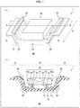
- Fig. 1 is a diagram schematically illustrating a configuration of a component-mounted body 1 (wiring substrate) in accordance with Embodiment 1.
- (a) of Fig. 1 is a perspective view of the component-mounted body 1.
- (b) of Fig. 1 is a cross-sectional view taken along a line A-A' as appears in (a) of Fig. 1 .
- a substrate for secondary mounting is not shown in Fig. 1 .
- the component-mounted body 1 in accordance with Embodiment 1 includes a wiring substrate 10, an IC chip 20 (electronic component), and bend assisting bodies 30.
- the wiring substrate 10 includes step-like portions so as to have a three-dimensional structure. Specifically, a depressed portion 14 is provided in a central part of an upper surface of the wiring substrate 10.
- the IC chip 20 is mounted in the depressed portion 14, to a bottom of the depressed portion 14, via flip chip mounting. More specifically, the step-like portions of the wiring substrate 10 are positioned so as to be opposite to lateral surfaces 20a of the IC chip 20 (see (b) of Fig. 1 ), which lateral surfaces 20a extend parallel to a TD axis as illustrated in (a) of Fig. 1 .
- the wiring substrate 10 includes a liquid crystal polymer (LCP) base material 11, a substrate wiring layer 12 (wiring) provided on an upper surface of the LCP base material 11, and a passivation layer 13 provided over the upper surface of the LCP base material 11 so as to cover part of the substrate wiring layer 12.
- LCP liquid crystal polymer
- a surface of the wiring substrate 10 on a side having the substrate wiring layer 12 and the passivation layer 13 is referred to as an upper surface
- a surface of the wiring substrate 10 on a side facing away from the upper surface is referred to as a lower surface.
- the upper surface (substrate surface) of the LCP base material 11 is quadrangular when the LCP base material 11 is flat. However, as illustrated in (a) of Fig. 1 , providing the step-like portions to the LCP base material 11 gives the LCP base material 11 a three-dimensional structure, in which the depressed portion 14 is formed in the central part of the upper surface.
- the upper surface of the LCP base material 11 includes the depressed portion 14 and two adjacent portions 15 which sandwich and are adjacent to the depressed portion 14 along an MD axis. In other words, a first one of the adjacent portions 15, the depressed portion 14, and a second one of the adjacent portions 15 are arranged in this order along the MD axis.
- the LCP base material 11 has a three-dimensional structure such that, in the above order along the MD axis, the LCP base material 11 is (i) contoured downwardly from the first one of the adjacent portions 15 to the bottom of the depressed portion 14 and (ii) contoured upwardly from the bottom of the depressed portion 14 to the second one of the adjacent portions 15.
- the terms "depressed portion 14" and “adjacent portions 15” may also be used to refer to the positions of the depressed portion 14 and the adjacent portions 15 on the wiring substrate 10.
- the LCP base material 11 is thermoplastic and has a thermal expansion coefficient which is anisotropic in the plane of the upper surface of the LCP base material 11. Specifically, a thermal expansion coefficient of the LCP base material 11 along a transverse direction (TD; perpendicular direction) axis (first axis) shown in (a) of Fig. 1 is greater than a thermal expansion coefficient of the LCP base material 11 along a machine direction (MD; flow direction) axis (second axis). For example, along the TD axis shown in (a) of Fig.
- the LCP base material 11 has a thermal expansion coefficient of approximately 5.0 ⁇ 10 -5 /°C to 10.0 ⁇ 10 -5 /°C, and along the MD axis shown in (a) of Fig. 1 , the LCP base material 11 has a thermal expansion coefficient of approximately 0.001 ⁇ 10 -5 /°C to 2.0 ⁇ 10 -5 /°C.
- Examples of a material for the LCP base material 11 include: a polycondensate of ethylene terephthalate and para-hydroxybenzoate; a polycondensate of (i) phenol and/or phthalic acid and (ii) para-hydroxybenzoate; and a polycondensate of 2,6-hydroxynaphthoic acid and para-hydroxybenzoate.
- a material for the LCP base material 11 is not, however, limited to these examples.
- the substrate wiring layer 12 constitutes a plurality of wires, each of which extends from (i) a vicinity of one of the two ends of the upper surface of the LCP base material 11, which ends extend parallel to the TD axis shown in (a) of Fig. 1 , toward (ii) the bottom of the depressed portion 14. As illustrated in (b) of Fig. 1 , each of the plurality of wires has a first end which is exposed at the bottom of the depressed portion 14 and a second end which is exposed at one of the adjacent portions 15.
- the number of wires which the substrate wiring layer 12 constitutes is not limited to that illustrated in (a) of Fig. 1 .
- the passivation layer 13 is formed so as to cover an intermediate portion of each of the wires constituted by the substrate wiring layer 12 (a portion which excludes the ends of each wire).
- the LCP base material 11 is film-like and flexible. Even in a state where the substrate wiring layer 12 and the passivation layer 13 are provided on the LCP base material 11 (i.e., in a state where the wiring substrate 10 is formed), the LCP base material 11 maintains the flexibility and the above-described anisotropy of the LCP base material 11.
- the IC chip 20 is an electronic component which is contained in the depressed portion 14 of the wiring substrate 10. Note that the IC chip 20 is completely contained in the depressed portion 14. In other words, a height of a top end of the IC chip 20 is approximately equal to the height of the adjacent portions 15. As such, in a case where mounting (so-called secondary mounting) is carried out by using solder to connect (i) terminals of the substrate wiring layer 12 (wiring / wires), which are provided to the adjacent portions 15 to (ii) wiring of a substrate for secondary mounting, the IC chip 20 does not hinder the mounting.
- the IC chip 20 has (i) a semiconductor base material 21 having a quadrangular shape, (ii) I/O pads 22 provided to a back surface of the semiconductor base material 21, the I/O pads 22 being terminals of an MMIC, (iii) Cu pillars 23 provided to the back surface of the semiconductor base material 21, and (iv) a solder layer 24 provided at tips of the Cu pillars 23.
- the I/O pads 22 and the Cu pillars 23 are provided to peripheral portions of the back surface of the quadrangular-shaped semiconductor base material 21 (for example, in a peripheral arrangement) so as to each be located in a position facing a respective one of connection terminals of the substrate wiring layer 12 (wiring / wires), which connection terminals are exposed at the bottom of the depressed portion 14 of the wiring substrate 10.
- an integrated circuit (IC) of the IC chip 20 may be a well-known high-frequency IC other than the MMIC, or may be any well-known IC without being restricted to a high-frequency one.
- each of the bend assisting bodies 30 is a belt-like layer extending parallel to the TD axis.
- the bend assisting bodies 30 are provided at a total of four positions, i.e., two positions on the upper surface of the wiring substrate 10, and two positions on the lower surface of the wiring substrate 10.
- each of the bend assisting bodies 30 is provided at a portion of the wiring substrate 10 that is bent.
- the portions of the wiring substrate that are bent are (i) boundary portions at a boundary between (a) the depressed portion 14 and (b) each of the adjacent portions 15 and (ii) boundary portions at a boundary between (a) the bottom portion of the depressed portion 14 and (b) each of the side portions of the depressed portion 14.
- the wiring substrate 10 is bent along a line extending parallel to the TD axis so that the upper surface of the wiring substrate 10 is on an outer side (convex side) of the bend.
- the wiring substrate 10 is bent along a line extending parallel to the TD axis so that the lower surface of the wiring substrate 10 is on an outer side of the bend.
- the bend assisting bodies 30 are provided so as to each cover the outer side of one of the bends. In other words, at the boundary portions between the depressed portion 14 and each one of the adjacent portions 15, the bend assisting bodies 30 are provided to the upper surface of the wiring substrate 10, and at the boundary portions between the bottom portion and each of the side portions of the depressed portion 14, the bend assisting bodies 30 are provided to the lower surface of the wiring substrate 10.
- Fig. 2 is a side view illustrating one portion of the wiring substrate 10 and one of the bend assisting bodies 30, as viewed from the same direction as in (b) of Fig. 1 .
- the LCP base material 11 (see Fig. 1 ), which is thermoplastic, serves as the base of the wiring substrate 10. Heating the wiring substrate 10 therefore causes the wiring substrate 10 to expand in accordance with the thermal expansion coefficients of the LCP base material 11.
- the bend assisting bodies 30 are made from a material which has a thermal expansion coefficient that is greater than the thermal expansion coefficient of the LCP base material 11 along the MD axis.
- FIG. 2 illustrates the wiring substrate 10 and one of the bend assisting bodies 30 in a state prior to heating.
- the bend assisting body 30 undergoes a greater degree of MD axis-wise expansion than does the wiring substrate 10, due to the difference between the thermal expansion coefficient of the bend assisting body 30 and the thermal expansion coefficient of the wiring substrate 10 along the MD axis.
- This causes the wiring substrate 10 to bend such that a side on which the bend assisting body 30 is not provided is on the inner side (concave side) of the bend, and a side having the bend assisting body 30 is on the outer side of the bend (see (b) of Fig. 2 ).
- the bend assisting body 30 causes the previously flat wiring substrate 10 to bend such that the above-described three-dimensional structure is formed.
- the bend assisting bodies 30 have a thermal expansion coefficient which is (i) greater than the thermal expansion coefficient of the LCP base material 11 along the MD axis and (ii) approximately equal to the thermal expansion coefficient of the LCP base material 11 along the TD axis.
- thermal expansion coefficient of LCP base material 11 along MD axis thermal expansion coefficient of LCP base material 11 along TD axis ⁇ thermal expansion coefficient of bend assisting bodies 30 Note that the thermal expansion coefficient of the bend assisting bodies 30 is isotropic.
- the wiring substrate 10 is not deformed with respect to the TD axis because the bend assisting bodies 30 and the wiring substrate 10 have approximately equal thermal expansion coefficients along the TD axis.
- the bend assisting bodies 30 cause the wiring substrate 10 to be deformed with respect to the MD axis because the bend assisting bodies 30 have a thermal expansion coefficient which is greater than that of the wiring substrate 10 along the MD axis.
- the wiring substrate 10 is bent so as to form a straight "bending line" parallel to the TD axis, the bend assisting bodies 30 being on an outer side of each bend.
- Fig. 3 is a perspective view of the wiring substrate 10 in a flat state, with the bend assisting bodies 30 being provided to the wiring substrate 10.
- each of the bend assisting bodies 30 is provided at a position at which the wiring substrate 10 is to bend, such that each of the bend assisting bodies 30 will be on an outer side of each bend.
- Each of the bend assisting bodies 30 extends in a belt-like manner parallel to the TD axis so as to span an entire TD axis-wise dimension of the wiring substrate 10.
- Providing the bend assisting bodies 30 in this manner makes it possible to form the depressed portion 14 and the adjacent portions 15 of the wiring substrate 10 by use of heating. This will be described later.
- Examples of a material for the bend assisting bodies 30 include resin and metal.
- resins which can be used include epoxy resin (thermal expansion coefficient of 2 ⁇ 10 -5 to 6.5 ⁇ 10 -5 ) and acrylic resin (thermal expansion coefficient of 4.5 ⁇ 10 -5 to 7.0 ⁇ 10 -5 ).
- metals which can be used include aluminum (thermal expansion coefficient of 23.0 ⁇ 10 -5 ), copper (thermal expansion coefficient of 16.8 ⁇ 10 -5 ), and gold (thermal expansion coefficient of 14.3 ⁇ 10 -5 ).
- Fig. 4 is a flowchart showing a method of producing the component-mounted body 1 illustrated in Fig. 1 .
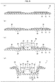
- Fig. 5 is a cross-sectional view for explaining steps of the method of producing the component-mounted body as shown in Fig. 4 .
- Each of (a) through (d) of Fig. 5 is a cross-sectional view of the wiring substrate 10 (LCP base material 11) and the like, as viewed from the same direction as in (b) of Fig. 1 .
- the wiring substrate 10 is prepared ( Fig. 4 : step S10, wiring forming step).
- the substrate wiring layer 12 e.g., Cu/Ni/Au
- the substrate wiring layer 12 constitutes (i) a wiring part, (ii) pads for connecting the IC chip, and (iii) I/O pads to be connected with, for example, wiring and another substrate.
- the passivation layer 13 is formed on the upper surface of the LCP base material 11 so as to cover the wiring part of the substrate wiring layer 12, which wiring part is not used for connection to an external element. This state is illustrated in (a) of Fig. 5 .
- the bend assisting bodies 30 are formed on the upper and lower surfaces of the wiring substrate 10 in a belt-like manner so that a longitudinal direction of the bend assisting bodies 30 is parallel to the TD axis ( Fig. 4 : step S11, bend assisting body forming step).
- the bend assisting bodies 30 are formed at positions as described above.
- the bend assisting bodies 30 formed on the upper surface of the wiring substrate 10 are provided above the substrate wiring layer 12 and the passivation layer 13. However, because the substrate wiring layer 12 and the passivation layer 13 are thin, they do not hinder bending of the LCP base material 11. Examples of a method of forming the bend assisting bodies 30, which are belt-like, include application with use of a dispenser, application by an inkjet method, and application by printing.
- the IC chip 20 illustrated in (c) of Fig. 5 is prepared ( Fig. 4 : step S20).
- the IC chip 20 which is prepared has (i) the MMIC (not illustrated) provided on the back surface of the semiconductor base material 21, (ii) the I/O pads 22, (iii) the Cu pillars 23 provided on the I/O pads 22 and having a height of, for example, 25 ⁇ m to 50 ⁇ m, and (iv) the solder layer 24 (e.g., SnAg solder) provided at the tip of the Cu pillars 23.
- the MMIC not illustrated
- the I/O pads 22 provided on the I/O pads 22 and having a height of, for example, 25 ⁇ m to 50 ⁇ m
- the solder layer 24 e.g., SnAg solder
- step S11 of Fig. 4 the IC chip 20 (prepared in step S20 of Fig. 4 ) is bonded ( Fig. 4 : step S12, contact step). This state is illustrated in (c) of Fig. 5 .
- reflow is carried out in a heated atmosphere ( Fig. 4 : step S13, heating step).
- the solder layer 24 provided to the IC chip 20 melts so that the terminals of the IC chip 20 are connected via the solder to IC chip-side pads of the substrate wiring layer 12.
- the wiring substrate 10 and the bend assisting bodies 30 bend so that the depressed portion 14 and the adjacent portions 15 are formed in the wiring substrate 10.
- the IC chip 20 becomes contained in the depressed portion 14.
- the formation of the depressed portion 14 happens concurrently with reflow.
- the reflow may be carried out using heat from a stage on which the wiring substrate 10 is placed, or heat from a tool etc. holding the IC chip 20. This state is illustrated in (d) of Fig. 5 .
- the heating is ended and cooling is performed (back to normal temperature) (cooling step).
- cooling step causes the solder layer 24 to be cured so that the connection between the IC chip 20 and the substrate wiring layer 12 via soldering is completed.
- the LCP base material 11 is thermoplastic, it maintains the above-described three-dimensional structure even after being cooled.
- the bend assisting bodies 30 may deform somewhat due to the cooling.
- Embodiment 1 providing the bend assisting bodies 30 makes it possible to form the depressed portion 14 in the wiring substrate 10 during reflow so that the IC chip 20 is contained in the depressed portion 14. In comparison to conventional techniques, this makes it possible to simplify a process for mounting an IC chip and forming a depressed portion in a wiring substrate. This simplification makes it possible to reduce, in comparison to conventional techniques, factors which can lead to faulty connections with the IC chip.
- the bend assisting bodies 30 are provided to the wiring substrate 10 before the IC chip 20 is bonded to the wiring substrate 10. Note, however, that the present invention is not limited to such a configuration.
- the bend assisting bodies 30 may be provided after the IC chip is bonded or simultaneously with the bonding of the IC chip.
- the component-mounted body 1 illustrated in (d) of Fig. 5 is first bonded to the wiring substrate for secondary mounting such that the substrate wiring layer 12 side of the wiring substrate 10 faces the wiring substrate for secondary mounting, and then reflow is carried out. In this way, it is possible to produce a secondary component-mounted body.
- the bend assisting bodies 30 have a thermal expansion coefficient which is (i) greater than the thermal expansion coefficient of the LCP base material 11 along the MD axis and (ii) approximately equal to the thermal expansion coefficient of the LCP base material 11 along the TD axis.
- the present invention is not, however, limited to such a configuration.
- a configuration can be employed in which the thermal expansion coefficient of the bend assisting bodies 30 is (i) greater than the thermal expansion coefficient of the LCP base material 11 along the MD axis but (ii) smaller than the thermal expansion coefficient of the LCP base material 11 along the TD axis.
- thermo expansion coefficient of LCP base material 11 along MD axis ⁇ (thermal expansion coefficient of bend assisting bodies 30) ⁇ (thermal expansion coefficient of LCP base material 11 along TD axis)
- the bend assisting bodies 30 bend due to the differences between (i) the thermal expansion coefficient of the bend assisting bodies 30 and (ii) the thermal expansion coefficients of the wiring substrate 10, along both of the TD axis direction and the MD axis direction.
- the difference in the MD axis direction is greater than the difference in the TD axis direction, bending with respect to the MD axis direction becomes predominant.
- the bend assisting bodies 30 have a thermal expansion coefficient which is (i) greater than the thermal expansion coefficient of the LCP base material 11 along the MD axis and (ii) approximately equal to the thermal expansion coefficient of the LCP base material 11 along the TD axis.
- the present invention is not, however, limited to such a configuration.
- a configuration can be employed in which the thermal expansion coefficient of the bend assisting bodies 30 is greater than both (i) the thermal expansion coefficient of the LCP base material 11 along the MD axis and (ii) the thermal expansion coefficient of the LCP base material 11 along the TD axis.
- thermal expansion coefficient of LCP base material 11 along MD axis ⁇ thermal expansion coefficient of LCP base material 11 along TD axis ⁇ thermal expansion coefficient of bend assisting bodies 30
- the bend assisting bodies 30 bend due to the differences between (i) the thermal expansion coefficient of the bend assisting bodies 30 and (ii) the thermal expansion coefficients of the wiring substrate 10, along both of the TD axis direction and the MD axis direction.
- the difference in the MD axis direction is greater than the difference in the TD axis direction, bending with respect to the MD axis direction becomes predominant.
- the component-mounted body in accordance with the present invention is not limited to the aspects discussed in Embodiment 1 and Variations 1 and 2 as illustrated in Fig. 1 .
- the component-mounted body 1 illustrated in Fig. 1 is configured such that the bend assisting bodies 30 covers outer sides of bends in the wiring substrate 10.
- the component-mounted body may, however, be alternatively configured as described below.
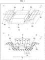
- Fig. 6 is a diagram schematically illustrating a configuration of a component-mounted body 2 in accordance with Embodiment 2.
- (a) of Fig. 6 is a top view of the component-mounted body 2.
- (b) of Fig. 6 is a cross-sectional view taken along a line A-A' as appears in (a) of Fig. 6 .
- members having functions similar to those described in Embodiment 1 are given the same reference signs, and the descriptions of such members are omitted.
- the component-mounted body 2 of Embodiment 2 as illustrated in Fig. 6 differs from the component-mounted body 1 of Embodiment 1 primarily with regards to the bend assisting bodies and the positions at which the bend assisting bodies are provided.
- bend assisting bodies 30a which are belt-like, are provided so as to extend in a MD axis direction of the wiring substrate 10, as illustrated in (a) of Fig. 6 .
- an upper surface of a wiring substrate 10a has a depressed portion 14 and two adjacent portions 15 which sandwich and are adjacent to the depressed portion 14 along a TD axis.
- a first one of the adjacent portions 15, the depressed portion 14, and a second one of the adjacent portions 15 are arranged in this order along the TD axis.
- An LCP base material 11 has a three-dimensional structure such that, in the above order along the TD axis, the LCP base material 11 is (i) contoured downwardly from the first one of the adjacent portions 15 to the bottom of the depressed portion 14 and (ii) contoured upwardly from the bottom of the depressed portion 14 to the second one of the adjacent portions 15.
- the direction in which the belt-like bend assisting bodies extends differs from that of Embodiment 1 by 90°.
- a direction in which wiring (constituted by a substrate wiring layer 12) extends also differs from that of Embodiment 1 by 90°.
- the component-mounted body 2 of Embodiment 2 is configured such that wiring thereof extends in a TD axis direction, from (i) a vicinity of one of either ends of the LCP base material 11, which ends extend parallel to the MD axis, toward (ii) the bottom of the depressed portion 14 of the LCP base material 11, as illustrated in (b) of Fig. 6 .
- each of the bend assisting bodies 30a is a belt-like layer extending parallel to the MD axis.
- the bend assisting bodies 30a are provided at a total of four positions, i.e., two positions on the upper surface of the wiring substrate 10a, and two positions on the lower surface of the wiring substrate 10a.
- the wiring substrate 10a is bent along a line extending parallel to the MD axis so that the upper surface of the wiring substrate 10a is on an outer side of the bend.
- the wiring substrate 10a is bent along a line extending parallel to the MD axis so that the lower surface of the wiring substrate 10a is on an outer side of the bend.
- the bend assisting bodies 30a are provided so as to cover a portion of a lower surface of the wiring substrate 10a.
- Each covered portion is on an inner side of a bend, and the upper surface of the wiring substrate 10a, which is on a reverse side, is on an outer side of the bend.
- the bend assisting bodies 30a are provided so as to cover a portion of the upper surface of the wiring substrate 10a, so that each covered portion is on an inner side of a bend.
- the bend assisting bodies 30a are made from a material which has a thermal expansion coefficient that is less than the thermal expansion coefficient of the LCP base material 11 along the TD axis.
- FIG. 7 illustrates the wiring substrate 10a and one of the bend assisting bodies 30a in a state prior to heating.
- the bend assisting body 30a undergoes a lesser degree of TD axis-wise expansion than does the wiring substrate 10a, due to the difference between the thermal expansion coefficient of the bend assisting body 30a and the thermal expansion coefficient of the wiring substrate 10a along the TD axis.
- This causes the wiring substrate 10a to bend such that a side on which the bend assisting body 30a is provided is on the inner side of the bend (see (b) of Fig. 7 ).
- the bend assisting bodies 30a have a thermal expansion coefficient which is (i) less than the thermal expansion coefficient of the LCP base material 11 along the TD axis and (ii) approximately equal to the thermal expansion coefficient of the LCP base material 11 along the MD axis.
- thermal expansion coefficient of bend assisting bodies 30 a ⁇ thermal expansion coefficient of LCP base material 11 along MD axis ⁇ thermal expansion coefficient of LCP base material 11 along TD axis Note that the thermal expansion coefficient of the bend assisting bodies 30a is isotropic.
- the wiring substrate 10a is not deformed with respect to the MD axis because the bend assisting bodies 30a and the wiring substrate 10a have approximately equal thermal expansion coefficients along the MD axis.
- the bend assisting bodies 30a cause the wiring substrate 10a to be deformed with respect to the TD axis because the bend assisting bodies 30a have a thermal expansion coefficient which is less than that of the wiring substrate 10a along the TD axis.
- the wiring substrate 10a is bent so as to form a straight "bending line" parallel to the MD axis, the bend assisting bodies 30a being on an inner side of each bend.
- Fig. 8 is a perspective view of the wiring substrate 10a in a flat state, with the bend assisting bodies 30a being provided to the wiring substrate 10a.
- each of the bend assisting bodies 30a is provided, in a belt-like manner parallel to the MD axis, at a position at which the wiring substrate 10a is to bend, such that each of the bend assisting bodies 30a will be on an inner side of each bend.
- Providing the bend assisting bodies 30a in this manner makes it possible to form the depressed portion 14 and the adjacent portions 15 of the wiring substrate 10a by use of heating.
- the LCP base material 11 can be made from a material having an MD axis thermal expansion coefficient of 2.0 ⁇ 10 -5 /°C and a TD axis thermal expansion coefficient of 8.9 ⁇ 10 -5 /°C.
- the bend assisting bodies 30a can be made of a material having a thermal expansion coefficient of 2 ⁇ 10 -5 /°C to 4 ⁇ 10 -5 /°C.
- LCP manufactured by Sumitomo Chemical Co., Ltd. product no. E6006L
- an epoxy resin manufactured by NTT Advanced Technology Corporation product nos. AT4291A, AT9290F, AT3083, and AT3088
- the wiring substrate 10a in a flat state can be caused to take on the three-dimensional structure concurrently with reflow, as with the component-mounted body 1 of Embodiment 1.
- a wiring substrate in accordance with an aspect of the present invention (which wiring substrate is also referred to as a first wiring substrate) includes:
- the above configuration makes it possible to provide a wiring substrate which allows bending of the wiring substrate to be carried out concurrently with reflow for mounting an electronic component to the wiring substrate.
- a bend assisting body which is belt-like and which satisfies the above conditions regarding thermal expansion coefficients makes it possible to bend the substrate, by use of heating, so that a bending line is formed along a straight line in which the bend assisting body extends. As such, it is possible to bend the substrate concurrently with reflow for mounting an electronic component, by using heat used for the reflow.
- the bend assisting body which (i) extends in a belt-like manner parallel to a first axis and (ii) satisfies the above conditions regarding thermal expansion coefficients makes it possible to bend the substrate and the wiring provided thereto in a manner such that (a) a side of the substrate to which the bend assisting body is provided is on an outer side of the bend and (b) a bending line extending parallel to the first axis is formed.
- another wiring substrate in accordance with an aspect of the present invention (which wiring substrate is also referred to as a second wiring substrate) includes:
- the above configuration makes it possible to provide a wiring substrate which allows bending of the wiring substrate to be carried out concurrently with reflow for mounting an electronic component to the wiring substrate.
- a bend assisting body which is belt-like and which satisfies the above conditions regarding thermal expansion coefficients makes it possible to bend the substrate, by use of heating, so that a bending line is formed along a straight line in which the bend assisting body extends. As such, it is possible to bend the substrate concurrently with reflow for mounting an electronic component, by using heat used for the reflow.
- the bend assisting body which (i) extends in a belt-like manner parallel to a second axis and (ii) satisfies the above conditions regarding thermal expansion coefficients makes it possible to bend the substrate and the wiring provided thereto in a manner such that (a) a side of the substrate to which the bend assisting body is provided is on an inner side of the bend and (b) a bending line extending parallel to the second axis is formed.
- the first wiring substrate in accordance with an embodiment of the present invention can be configured such that: the thermal expansion coefficient of the at least one bend assisting body is equal or substantially equal to the first thermal expansion coefficient of the substrate.
- a difference between the thermal expansion coefficient of the at least one bend assisting body and the first thermal expansion coefficient is either nonexistent or negligible.
- a force which the at least one bend assisting body exerts on the substrate so as to bend the substrate with respect to the first axis is nonexistent or negligible.
- the thermal expansion coefficient of the at least one bend assisting body being "substantially equal" to the first thermal expansion coefficient of the substrate means that the difference between (i) the thermal expansion coefficient of the at least one bend assisting body and (ii) the first thermal expansion coefficient of the substrate is sufficiently small compared to (i) the thermal expansion coefficient of the at least one bend assisting body or (ii) the first thermal expansion coefficient of the substrate.
- the second wiring substrate in accordance with an embodiment of the present invention can be configured such that: the thermal expansion coefficient of the at least one bend assisting body is equal or substantially equal to the second thermal expansion coefficient of the substrate.
- a difference between the thermal expansion coefficient of the at least one bend assisting body and the first thermal expansion coefficient is either nonexistent or negligible.
- a force which the at least one bend assisting body exerts on the substrate so as to bend the substrate with respect to the first axis is nonexistent or negligible.
- the thermal expansion coefficient of the at least one bend assisting body being "substantially equal" to the second thermal expansion coefficient of the substrate means that the difference between (i) the thermal expansion coefficient of the at least one bend assisting body and (ii) the second thermal expansion coefficient of the substrate is sufficiently small compared to (i) the thermal expansion coefficient of the at least one bend assisting body or (ii) the second thermal expansion coefficient of the substrate.
- the above configuration makes it possible to provide a wiring substrate in the form of a primary component-mounted body in which an electronic component is contained in a depressed portion of the wiring substrate.
- the above configuration makes it possible to provide a liquid crystal polymer substrate which enables simplification of an operation for mounting an electronic component thereto.
- a method of producing a wiring substrate in accordance with an aspect of the present invention (which method is also referred to as a first method of producing a wiring substrate) includes:
- the above configuration makes it possible to provide a wiring substrate which allows bending of the wiring substrate to be carried out concurrently with reflow for mounting an electronic component to the wiring substrate.
- a bend assisting body which is belt-like and which satisfies the above conditions regarding thermal expansion coefficients makes it possible to bend the substrate, by use of heating, so that a bending line is formed along a straight line in which the bend assisting body extends. As such, it is possible to bend the substrate concurrently with reflow for mounting an electronic component, by using heat used for the reflow.
- the bend assisting body which (i) extends in a belt-like manner parallel to a first axis and (ii) satisfies the above conditions regarding thermal expansion coefficients makes it possible to bend the substrate and the wiring provided thereto in a manner such that (a) a side of the substrate to which the bend assisting body is provided is on an outer side of the bend and (b) a bending line extending parallel to the first axis is formed.
- Another method of producing a wiring substrate in accordance with an aspect of the present invention includes the steps of:
- the above configuration makes it possible to provide a wiring substrate which allows bending of the wiring substrate to be carried out concurrently with reflow for mounting an electronic component to the wiring substrate.
- a bend assisting body which is belt-like and which satisfies the above conditions regarding thermal expansion coefficients makes it possible to bend the substrate, by use of heating, so that a bending line is formed along a straight line in which the bend assisting body extends. As such, it is possible to bend the substrate concurrently with reflow for mounting an electronic component, by using heat used for the reflow.
- the bend assisting body which (i) extends in a belt-like manner parallel to a second axis and (ii) satisfies the above conditions regarding thermal expansion coefficients makes it possible to bend the substrate and the wiring provided thereto in a manner such that (a) a side of the substrate to which the bend assisting body is provided is on an inner side of the bend and (b) a bending line extending parallel to the second axis is formed.
- the above configuration makes it possible to provide a wiring substrate in the form of a primary component-mounted body in which an electronic component is contained in a depressed portion of the wiring substrate.
- the present invention is not limited to the embodiments, but can be altered by a skilled person in the art within the scope of the claims.
- the present invention also encompasses, in its technical scope, any embodiment derived by combining technical means disclosed in differing embodiments.
Landscapes
- Engineering & Computer Science (AREA)
- Microelectronics & Electronic Packaging (AREA)
- Manufacturing & Machinery (AREA)
- Structure Of Printed Boards (AREA)
- Laminated Bodies (AREA)
Abstract
Description
- The present invention relates to a wiring substrate and a method of producing the wiring substrate.
-
Patent Literature 1 discloses an electronic device in which an electronic component is provided to a depressed portion of a supporting body made of a liquid crystal polymer. Containing the electronic component in the depressed portion of the support is advantageous in that it makes it possible to prevent the electronic component from become a hindrance to mounting the support body to another support body (i.e., secondary mounting). Furthermore, liquid crystal polymer has excellent electrical properties, size stability, and heat resistance, and a layer of metal such as copper foil can be provided directly thereto via heating. This allows the liquid crystal polymer to be suitably used as a substrate for an electronic circuit. - A more detailed description of a component-mounted body obtained as a result of secondary mounting is as follows (such a body is hereinafter referred to as a "secondary component-mounted body").
Fig. 9 is a perspective view of an example of a secondary component-mounted body. Note that inFig. 9 , for convenience, a substrate for secondary mounting is depicted as a transparent member. As illustrated inFig. 9 , asubstrate 111 for primary mounting has adepressed portion 114, in which anelectronic component 120 is contained. Terminals of theelectronic component 120 are connected via soldering 124, to first ends ofwiring 112 provided to thesubstrate 111 for primary mounting. Second ends of thewiring 112 are connected, via soldering 150, to terminals (not shown) of asubstrate 140 for secondary mounting. - Discussed next, with reference to
Fig. 10 , is a typical process of producing the secondary component-mounted body illustratedFig. 9 .Fig. 10 is a side view of an electronic component, a substrate for primary mounting, and a substrate for secondary mounting. There are two general types of production processes involving the steps illustrated inFig. 10 . The first type of production process is as follows. Thesubstrate 111 for primary mounting begins in the state illustrated in (a) ofFig. 10 , in which a depressed portion has not yet been formed. Theelectronic component 120 is placed on thissubstrate 111, and terminals of theelectronic component 120 are electrically connected to thewiring 112 of the substrate 111 ((b) ofFig. 10 ). Thesubstrate 111 is then bent so as to form thedepressed portion 114 which contains the electronic component 120 ((d) ofFig. 10 ). Finally, thesubstrate 111 for primary mounting is electrically connected to thesubstrate 140 for secondary mounting ((e) ofFig. 10 ), and the secondary component-mounted body is completed. The second type of production process is as follows. Thesubstrate 111 for primary mounting begins in the state illustrated in (a) ofFig. 10 , in which a depressed portion has not yet been formed. Before theelectronic component 120 is mounted to thesubstrate 111, thesubstrate 111 is bent so that thedepressed portion 114 is formed ((c) ofFig. 10 ). Thereafter, theelectronic component 120 is placed so as to be contained in thedepressed portion 114, and terminals of theelectronic component 120 are electrically connected to the wiring of the substrate 111 ((d) ofFig. 10 ). Finally, connection terminals ofsubstrate 111 for primary mounting are electrically connected to connection terminals of thesubstrate 140 for secondary mounting ((e) ofFig. 10 ), and the secondary component-mounted body is completed. - [Patent Literature 1] Japanese Patent Application Publication, Tokukai, No.
2004-82564 (Publication Date: March 18, 2004 - With such a conventional production method, it is necessary to carry out an operation to bend the substrate either before or after the operation to mount the electronic component to the substrate, as illustrated in
Fig. 10 . - In the first type of production process described above, the substrate is bent after the electronic component is mounted thereto. As such, there is a risk that a worker, an instrument used by a worker, or the like will make contact with the electronic component during the operation to bend the substrate and result in a faulty connection. In the second type of production process described above, the substrate is bent before the electronic component is mounted thereto. In this case, it is necessary to mount the electronic component to a bent substrate. This increases the difficulty of the operation for mounting the electronic component and increases the likelihood of a faulty connection stemming from an error in the mounting operation.
- An embodiment of the present invention is accomplished in view of the above problems. An object of an embodiment of the present invention lies in providing (i) a wiring substrate which allows bending of the wiring substrate to be carried out concurrently with reflow for mounting an electronic component to the wiring substrate, and (ii) a method of producing such a wiring substrate.
- In order to solve the above-described problems, a wiring substrate in accordance with an aspect of the present invention (which wiring substrate is also referred to as a first wiring substrate) includes:
- a substrate which is thermoplastic, the substrate having a first thermal expansion coefficient and a second thermal expansion coefficient, the first thermal expansion coefficient being relative to a first axis which is parallel to a substrate surface of the substrate, the second thermal expansion coefficient being relative to a second axis which (i) is parallel to the substrate surface and (ii) intersects with the first axis, the first thermal expansion coefficient being greater than the second thermal expansion coefficient;
- wiring formed on the substrate; and
- at least one bend assisting body which extends in a belt-like manner parallel to the first axis of the substrate surface,
- a difference between (i) a thermal expansion coefficient of the at least one bend assisting body and (ii) the second thermal expansion coefficient of the substrate being greater than a difference between (i) the thermal expansion coefficient of the at least one bend assisting body and (ii) the first thermal expansion coefficient of the substrate,
- the substrate being bent along with each of the at least one bend assisting body so as to form a bending line which extends parallel to the first axis.
- In order to solve the above-described problems, another wiring substrate in accordance with an aspect of the present invention (which wiring substrate is also referred to as a second wiring substrate) includes:
- a substrate which is thermoplastic, the substrate having a first thermal expansion coefficient and a second thermal expansion coefficient, the first thermal expansion coefficient being relative to a first axis which is parallel to a substrate surface of the substrate, the second thermal expansion coefficient being relative to a second axis which (i) is parallel to the substrate surface and (ii) intersects with the first axis, the first thermal expansion coefficient being greater than the second thermal expansion coefficient;
- wiring formed on the substrate; and
- at least one bend assisting body which extends in a belt-like manner parallel to the second axis of the substrate surface,
- a difference between (i) a thermal expansion coefficient of the at least one bend assisting body and (ii) the first thermal expansion coefficient of the substrate being greater than a difference between (i) the thermal expansion coefficient of the at least one bend assisting body and (ii) the second thermal expansion coefficient of the substrate,
- the substrate being bent along with each of the at least one bend assisting body so as to form a bending line which extends parallel to the second axis.
- A method of producing a wiring substrate in accordance with an aspect of the present invention (which method is also referred to as a first method of producing a wiring substrate) includes the steps of:
- forming wiring on a substrate which is thermoplastic, the substrate having a first thermal expansion coefficient and a second thermal expansion coefficient, the first thermal expansion coefficient being relative to a first axis which is parallel to a substrate surface of the substrate, the second thermal expansion coefficient being relative to a second axis which (i) is parallel to the substrate surface and (ii) intersects with the first axis, the first thermal expansion coefficient being greater than the second thermal expansion coefficient;
- forming, on the substrate, at least one bend assisting body which extends in a belt-like manner parallel to the first axis of the substrate surface, the at least one bend assisting body having a thermal expansion coefficient such that a difference between (i) the thermal expansion coefficient of the at least one bend assisting body and (ii) the second thermal expansion coefficient of the substrate is greater than a difference between (i) the thermal expansion coefficient of the at least one bend assisting body and (ii) the first thermal expansion coefficient of the substrate; and
- heating the substrate and the bend assisting body after the step of forming the at least one bend assisting body, such that the substrate is bent along with each of the at least one bend assisting body so as to form a bending line which extends parallel to the first axis.
- In order to solve the above-described problems, another method of producing a wiring substrate in accordance with an aspect of the present invention (which method is also referred to as a second method of producing a wiring substrate) includes the steps of:
- forming wiring on a substrate which is thermoplastic, the substrate having a first thermal expansion coefficient and a second thermal expansion coefficient, the first thermal expansion coefficient being relative to a first axis which is parallel to a substrate surface of the substrate, the second thermal expansion coefficient being relative to a second axis which (i) is parallel to the substrate surface and (ii) intersects with the first axis, the first thermal expansion coefficient being greater than the second thermal expansion coefficient;
- forming, on the substrate, at least one bend assisting body which extends in a belt-like manner parallel to the second axis of the substrate surface, the at least one bend assisting body having a thermal expansion coefficient such that a difference between (i) the thermal expansion coefficient of the at least one bend assisting body and (ii) the first thermal expansion coefficient of the substrate is greater than a difference between (i) the thermal expansion coefficient of the at least one bend assisting body and (ii) the second thermal expansion coefficient of the substrate; and
- heating the substrate and the bend assisting body after the step of forming the at least one bend assisting body, such that the substrate is bent along with each of the at least one bend assisting body so as to form a bending line which extends parallel to the second axis.
- An embodiment of the present invention makes it possible to provide a wiring substrate which allows bending of the wiring substrate to be carried out concurrently with reflow for mounting an electronic component to the wiring substrate.
-
-
Fig. 1 is a diagram schematically illustrating a configuration of a component-mounted body in accordance with an embodiment of the present invention. (a) ofFig. 1 is a perspective view of the component-mounted body. (b) ofFig. 1 is a cross-sectional view taken along a line A-A' as appears in (a) ofFig. 1 . -
Fig. 2 is a lateral view of a portion of the component-mounted body illustrated inFig. 1 . (a) ofFig. 2 illustrates the component-mounted body prior to heating. (b) ofFig. 2 illustrates the component-mounted body after heating. -
Fig. 3 is a perspective view of a portion of the component-mounted body illustrated inFig. 1 . -
Fig. 4 is a flowchart illustrating a method for manufacturing the component-mounted body illustrated inFig. 1 . -
Fig. 5 is a diagram for explaining steps of producing the component-mounted body illustrated inFig. 1 . -
Fig. 6 is a diagram schematically illustrating a configuration of a component-mounted body in accordance with another embodiment of the present invention. (a) ofFig. 6 is a perspective view of the component-mounted body. (b) ofFig. 6 is a cross-sectional view taken along a line A-A' as appears in (a) ofFig. 6 . -
Fig. 7 is a lateral view of a portion of the component-mounted body illustrated inFig. 6 . (a) ofFig. 7 illustrates the component-mounted body prior to heating. (b) ofFig. 7 illustrates the component-mounted body after heating. -
Fig. 8 is a perspective view of a portion of the component-mounted body illustrated inFig. 1 . -
Fig. 9 is a diagram for explaining a conventional configuration. -
Fig. 10 is a diagram for explaining a conventional configuration. - The following description will discuss a wiring substrate and a method of producing the wiring substrate in accordance with an embodiment of the present invention.
- Note that in the following descriptions, the term "component-mounted body" is used to refer to a body including a wiring substrate and an IC chip (one type of electronic component) mounted to the wiring substrate. Furthermore, in the following descriptions, the electronic component (IC chip) and a bend assisting body are discussed as being elements which are separate from the wiring substrate. However, the term "wiring substrate" may be used to refer to (i) a wiring substrate which includes a bend assisting body and (ii) a wiring substrate which includes a bend assisting body and an electronic component (IC chip).
-
Fig. 1 is a diagram schematically illustrating a configuration of a component-mounted body 1 (wiring substrate) in accordance withEmbodiment 1. (a) ofFig. 1 is a perspective view of the component-mountedbody 1. (b) ofFig. 1 is a cross-sectional view taken along a line A-A' as appears in (a) ofFig. 1 . For ease of explanation, a substrate for secondary mounting is not shown inFig. 1 . - As illustrated in (a) of
Fig. 1 , the component-mountedbody 1 in accordance withEmbodiment 1 includes awiring substrate 10, an IC chip 20 (electronic component), andbend assisting bodies 30. Thewiring substrate 10 includes step-like portions so as to have a three-dimensional structure. Specifically, adepressed portion 14 is provided in a central part of an upper surface of thewiring substrate 10. TheIC chip 20 is mounted in thedepressed portion 14, to a bottom of thedepressed portion 14, via flip chip mounting. More specifically, the step-like portions of thewiring substrate 10 are positioned so as to be opposite tolateral surfaces 20a of the IC chip 20 (see (b) ofFig. 1 ), which lateral surfaces 20a extend parallel to a TD axis as illustrated in (a) ofFig. 1 . - As illustrated in (b) of
Fig. 1 , thewiring substrate 10 includes a liquid crystal polymer (LCP)base material 11, a substrate wiring layer 12 (wiring) provided on an upper surface of theLCP base material 11, and apassivation layer 13 provided over the upper surface of theLCP base material 11 so as to cover part of thesubstrate wiring layer 12. In the descriptions below, a surface of thewiring substrate 10 on a side having thesubstrate wiring layer 12 and thepassivation layer 13 is referred to as an upper surface, and a surface of thewiring substrate 10 on a side facing away from the upper surface is referred to as a lower surface. - The upper surface (substrate surface) of the
LCP base material 11 is quadrangular when theLCP base material 11 is flat. However, as illustrated in (a) ofFig. 1 , providing the step-like portions to theLCP base material 11 gives the LCP base material 11 a three-dimensional structure, in which thedepressed portion 14 is formed in the central part of the upper surface. The upper surface of theLCP base material 11 includes thedepressed portion 14 and twoadjacent portions 15 which sandwich and are adjacent to thedepressed portion 14 along an MD axis. In other words, a first one of theadjacent portions 15, thedepressed portion 14, and a second one of theadjacent portions 15 are arranged in this order along the MD axis. TheLCP base material 11 has a three-dimensional structure such that, in the above order along the MD axis, theLCP base material 11 is (i) contoured downwardly from the first one of theadjacent portions 15 to the bottom of thedepressed portion 14 and (ii) contoured upwardly from the bottom of thedepressed portion 14 to the second one of theadjacent portions 15. Note that the terms "depressed portion 14" and "adjacent portions 15" may also be used to refer to the positions of thedepressed portion 14 and theadjacent portions 15 on thewiring substrate 10. - The
LCP base material 11 is thermoplastic and has a thermal expansion coefficient which is anisotropic in the plane of the upper surface of theLCP base material 11. Specifically, a thermal expansion coefficient of theLCP base material 11 along a transverse direction (TD; perpendicular direction) axis (first axis) shown in (a) ofFig. 1 is greater than a thermal expansion coefficient of theLCP base material 11 along a machine direction (MD; flow direction) axis (second axis). For example, along the TD axis shown in (a) ofFig. 1 , theLCP base material 11 has a thermal expansion coefficient of approximately 5.0 × 10⁻⁵/°C to 10.0 × 10⁻⁵/°C, and along the MD axis shown in (a) ofFig. 1 , theLCP base material 11 has a thermal expansion coefficient of approximately 0.001 × 10⁻⁵/°C to 2.0 × 10⁻⁵/°C. - Examples of a material for the
LCP base material 11 include: a polycondensate of ethylene terephthalate and para-hydroxybenzoate; a polycondensate of (i) phenol and/or phthalic acid and (ii) para-hydroxybenzoate; and a polycondensate of 2,6-hydroxynaphthoic acid and para-hydroxybenzoate. A material for theLCP base material 11 is not, however, limited to these examples. - The
substrate wiring layer 12 constitutes a plurality of wires, each of which extends from (i) a vicinity of one of the two ends of the upper surface of theLCP base material 11, which ends extend parallel to the TD axis shown in (a) ofFig. 1 , toward (ii) the bottom of thedepressed portion 14. As illustrated in (b) ofFig. 1 , each of the plurality of wires has a first end which is exposed at the bottom of thedepressed portion 14 and a second end which is exposed at one of theadjacent portions 15. The number of wires which thesubstrate wiring layer 12 constitutes is not limited to that illustrated in (a) ofFig. 1 . - The
passivation layer 13 is formed so as to cover an intermediate portion of each of the wires constituted by the substrate wiring layer 12 (a portion which excludes the ends of each wire). - Note that in
Embodiment 1, theLCP base material 11 is film-like and flexible. Even in a state where thesubstrate wiring layer 12 and thepassivation layer 13 are provided on the LCP base material 11 (i.e., in a state where thewiring substrate 10 is formed), theLCP base material 11 maintains the flexibility and the above-described anisotropy of theLCP base material 11. - The
IC chip 20 is an electronic component which is contained in thedepressed portion 14 of thewiring substrate 10. Note that theIC chip 20 is completely contained in thedepressed portion 14. In other words, a height of a top end of theIC chip 20 is approximately equal to the height of theadjacent portions 15. As such, in a case where mounting (so-called secondary mounting) is carried out by using solder to connect (i) terminals of the substrate wiring layer 12 (wiring / wires), which are provided to theadjacent portions 15 to (ii) wiring of a substrate for secondary mounting, theIC chip 20 does not hinder the mounting. - As illustrated in (b) of
Fig. 1 , theIC chip 20 has (i) asemiconductor base material 21 having a quadrangular shape, (ii) I/O pads 22 provided to a back surface of thesemiconductor base material 21, the I/O pads 22 being terminals of an MMIC, (iii)Cu pillars 23 provided to the back surface of thesemiconductor base material 21, and (iv) asolder layer 24 provided at tips of theCu pillars 23. The I/O pads 22 and theCu pillars 23 are provided to peripheral portions of the back surface of the quadrangular-shaped semiconductor base material 21 (for example, in a peripheral arrangement) so as to each be located in a position facing a respective one of connection terminals of the substrate wiring layer 12 (wiring / wires), which connection terminals are exposed at the bottom of thedepressed portion 14 of thewiring substrate 10. Note that an integrated circuit (IC) of theIC chip 20 may be a well-known high-frequency IC other than the MMIC, or may be any well-known IC without being restricted to a high-frequency one. - As illustrated in (a) of
Fig. 1 , each of thebend assisting bodies 30 is a belt-like layer extending parallel to the TD axis. Thebend assisting bodies 30 are provided at a total of four positions, i.e., two positions on the upper surface of thewiring substrate 10, and two positions on the lower surface of thewiring substrate 10. - More specifically, each of the
bend assisting bodies 30 is provided at a portion of thewiring substrate 10 that is bent. The portions of the wiring substrate that are bent are (i) boundary portions at a boundary between (a) thedepressed portion 14 and (b) each of theadjacent portions 15 and (ii) boundary portions at a boundary between (a) the bottom portion of thedepressed portion 14 and (b) each of the side portions of thedepressed portion 14. At the boundary portions between thedepressed portion 14 and each of theadjacent portions 15, thewiring substrate 10 is bent along a line extending parallel to the TD axis so that the upper surface of thewiring substrate 10 is on an outer side (convex side) of the bend. At the boundary portions between the bottom portion and each of the side portions of thedepressed portion 14, thewiring substrate 10 is bent along a line extending parallel to the TD axis so that the lower surface of thewiring substrate 10 is on an outer side of the bend. Thebend assisting bodies 30 are provided so as to each cover the outer side of one of the bends. In other words, at the boundary portions between thedepressed portion 14 and each one of theadjacent portions 15, thebend assisting bodies 30 are provided to the upper surface of thewiring substrate 10, and at the boundary portions between the bottom portion and each of the side portions of thedepressed portion 14, thebend assisting bodies 30 are provided to the lower surface of thewiring substrate 10. - The following description will discuss the
bend assisting bodies 30 in detail, with reference toFig. 2. Fig. 2 is a side view illustrating one portion of thewiring substrate 10 and one of thebend assisting bodies 30, as viewed from the same direction as in (b) ofFig. 1 . - The LCP base material 11 (see
Fig. 1 ), which is thermoplastic, serves as the base of thewiring substrate 10. Heating thewiring substrate 10 therefore causes thewiring substrate 10 to expand in accordance with the thermal expansion coefficients of theLCP base material 11. InEmbodiment 1, thebend assisting bodies 30 are made from a material which has a thermal expansion coefficient that is greater than the thermal expansion coefficient of theLCP base material 11 along the MD axis. - (a) of
Fig. 2 illustrates thewiring substrate 10 and one of thebend assisting bodies 30 in a state prior to heating. When thewiring substrate 10 and thebend assisting body 30 are heated, thebend assisting body 30 undergoes a greater degree of MD axis-wise expansion than does thewiring substrate 10, due to the difference between the thermal expansion coefficient of thebend assisting body 30 and the thermal expansion coefficient of thewiring substrate 10 along the MD axis. This causes thewiring substrate 10 to bend such that a side on which thebend assisting body 30 is not provided is on the inner side (concave side) of the bend, and a side having thebend assisting body 30 is on the outer side of the bend (see (b) ofFig. 2 ). - In other words, the
bend assisting body 30 causes the previouslyflat wiring substrate 10 to bend such that the above-described three-dimensional structure is formed. - Note that in the present specification, the word "bend" encompasses both (i) sharp bending and (ii) curving.
- More specifically, the
bend assisting bodies 30 have a thermal expansion coefficient which is (i) greater than the thermal expansion coefficient of theLCP base material 11 along the MD axis and (ii) approximately equal to the thermal expansion coefficient of theLCP base material 11 along the TD axis. - In other words, the following relational expression holds true.

bend assisting bodies 30 is isotropic. - With the above thermal expansion coefficients, the
wiring substrate 10 is not deformed with respect to the TD axis because thebend assisting bodies 30 and thewiring substrate 10 have approximately equal thermal expansion coefficients along the TD axis. However, thebend assisting bodies 30 cause thewiring substrate 10 to be deformed with respect to the MD axis because thebend assisting bodies 30 have a thermal expansion coefficient which is greater than that of thewiring substrate 10 along the MD axis. Specifically, at each position where one of thebend assisting bodies 30 is provided, thewiring substrate 10 is bent so as to form a straight "bending line" parallel to the TD axis, thebend assisting bodies 30 being on an outer side of each bend. -
Fig. 3 is a perspective view of thewiring substrate 10 in a flat state, with thebend assisting bodies 30 being provided to thewiring substrate 10. As illustrated inFig. 3 , on thewiring substrate 10 in a flat state, each of thebend assisting bodies 30 is provided at a position at which thewiring substrate 10 is to bend, such that each of thebend assisting bodies 30 will be on an outer side of each bend. Each of thebend assisting bodies 30 extends in a belt-like manner parallel to the TD axis so as to span an entire TD axis-wise dimension of thewiring substrate 10. - Providing the
bend assisting bodies 30 in this manner makes it possible to form thedepressed portion 14 and theadjacent portions 15 of thewiring substrate 10 by use of heating. This will be described later. - Examples of a material for the
bend assisting bodies 30 include resin and metal. Examples of resins which can be used include epoxy resin (thermal expansion coefficient of 2 × 10⁻⁵ to 6.5 × 10⁻⁵) and acrylic resin (thermal expansion coefficient of 4.5 × 10⁻⁵ to 7.0 × 10⁻⁵). Examples of metals which can be used include aluminum (thermal expansion coefficient of 23.0 × 10⁻⁵), copper (thermal expansion coefficient of 16.8 × 10⁻⁵), and gold (thermal expansion coefficient of 14.3 × 10⁻⁵). - Note that a greater difference between the respective thermal expansion coefficients of the
LCP base material 11 and thebend assisting bodies 30 will lead to a greater degree of bending when theLCP base material 11 and thebend assisting bodies 30 are heated. It is therefore possible to change the degree of bending by adjusting the difference between these thermal expansion coefficients. - The following description will discuss, with reference to
Figs. 4 and5 , a method of producing the component-mountedbody 1 in accordance withEmbodiment 1.Fig. 4 is a flowchart showing a method of producing the component-mountedbody 1 illustrated inFig. 1 .Fig. 5 is a cross-sectional view for explaining steps of the method of producing the component-mounted body as shown inFig. 4 . Each of (a) through (d) ofFig. 5 is a cross-sectional view of the wiring substrate 10 (LCP base material 11) and the like, as viewed from the same direction as in (b) ofFig. 1 . - First, the
wiring substrate 10 is prepared (Fig. 4 : step S10, wiring forming step). Specifically, the substrate wiring layer 12 (e.g., Cu/Ni/Au) is formed on the upper surface of theLCP base material 11 by a method such as plating. Thesubstrate wiring layer 12 constitutes (i) a wiring part, (ii) pads for connecting the IC chip, and (iii) I/O pads to be connected with, for example, wiring and another substrate. Further, thepassivation layer 13 is formed on the upper surface of theLCP base material 11 so as to cover the wiring part of thesubstrate wiring layer 12, which wiring part is not used for connection to an external element. This state is illustrated in (a) ofFig. 5 . - Next, the
bend assisting bodies 30 are formed on the upper and lower surfaces of thewiring substrate 10 in a belt-like manner so that a longitudinal direction of thebend assisting bodies 30 is parallel to the TD axis (Fig. 4 : step S11, bend assisting body forming step). Thebend assisting bodies 30 are formed at positions as described above. Thebend assisting bodies 30 formed on the upper surface of thewiring substrate 10 are provided above thesubstrate wiring layer 12 and thepassivation layer 13. However, because thesubstrate wiring layer 12 and thepassivation layer 13 are thin, they do not hinder bending of theLCP base material 11. Examples of a method of forming thebend assisting bodies 30, which are belt-like, include application with use of a dispenser, application by an inkjet method, and application by printing. - The
IC chip 20 illustrated in (c) ofFig. 5 is prepared (Fig. 4 : step S20). Specifically, theIC chip 20 which is prepared has (i) the MMIC (not illustrated) provided on the back surface of thesemiconductor base material 21, (ii) the I/O pads 22, (iii) theCu pillars 23 provided on the I/O pads 22 and having a height of, for example, 25 µm to 50 µm, and (iv) the solder layer 24 (e.g., SnAg solder) provided at the tip of theCu pillars 23. - Next, to the upper surface of the wiring substrate 10 (on which the
bend assisting bodies 30 were formed in step S11 ofFig. 4 ), the IC chip 20 (prepared in step S20 ofFig. 4 ) is bonded (Fig. 4 : step S12, contact step). This state is illustrated in (c) ofFig. 5 . - Subsequently, reflow is carried out in a heated atmosphere (
Fig. 4 : step S13, heating step). In the heated atmosphere, thesolder layer 24 provided to theIC chip 20 melts so that the terminals of theIC chip 20 are connected via the solder to IC chip-side pads of thesubstrate wiring layer 12. Also, thewiring substrate 10 and thebend assisting bodies 30 bend so that thedepressed portion 14 and theadjacent portions 15 are formed in thewiring substrate 10. At this time, theIC chip 20 becomes contained in thedepressed portion 14. In other words, the formation of thedepressed portion 14 happens concurrently with reflow. Note that the reflow may be carried out using heat from a stage on which thewiring substrate 10 is placed, or heat from a tool etc. holding theIC chip 20. This state is illustrated in (d) ofFig. 5 . - Then, at a step S14 shown in
Fig. 4 , the heating is ended and cooling is performed (back to normal temperature) (cooling step). This causes thesolder layer 24 to be cured so that the connection between theIC chip 20 and thesubstrate wiring layer 12 via soldering is completed. Because theLCP base material 11 is thermoplastic, it maintains the above-described three-dimensional structure even after being cooled. Thebend assisting bodies 30 may deform somewhat due to the cooling. - In this way, the component-mounted
body 1 in accordance withEmbodiment 1 is completed. - In
Embodiment 1, providing thebend assisting bodies 30 makes it possible to form thedepressed portion 14 in thewiring substrate 10 during reflow so that theIC chip 20 is contained in thedepressed portion 14. In comparison to conventional techniques, this makes it possible to simplify a process for mounting an IC chip and forming a depressed portion in a wiring substrate. This simplification makes it possible to reduce, in comparison to conventional techniques, factors which can lead to faulty connections with the IC chip. - In the production method in accordance with
Embodiment 1, thebend assisting bodies 30 are provided to thewiring substrate 10 before theIC chip 20 is bonded to thewiring substrate 10. Note, however, that the present invention is not limited to such a configuration. Thebend assisting bodies 30 may be provided after the IC chip is bonded or simultaneously with the bonding of the IC chip. - When secondary mounting is to be carried out, the component-mounted
body 1 illustrated in (d) ofFig. 5 is first bonded to the wiring substrate for secondary mounting such that thesubstrate wiring layer 12 side of thewiring substrate 10 faces the wiring substrate for secondary mounting, and then reflow is carried out. In this way, it is possible to produce a secondary component-mounted body. - In
Embodiment 1, thebend assisting bodies 30 have a thermal expansion coefficient which is (i) greater than the thermal expansion coefficient of theLCP base material 11 along the MD axis and (ii) approximately equal to the thermal expansion coefficient of theLCP base material 11 along the TD axis. The present invention is not, however, limited to such a configuration. - For example, a configuration can be employed in which the thermal expansion coefficient of the
bend assisting bodies 30 is (i) greater than the thermal expansion coefficient of theLCP base material 11 along the MD axis but (ii) smaller than the thermal expansion coefficient of theLCP base material 11 along the TD axis. - In other words, a configuration can be employed in which the following relational expression holds true.
(thermal expansion coefficient ofLCP base material 11 along MD axis) < (thermal expansion coefficient of bend assisting bodies 30) < (thermal expansion coefficient ofLCP base material 11 along TD axis) - However, in such a configuration, the following relational expression is to be satisfied.

- With the above thermal expansion coefficients, the
bend assisting bodies 30 bend due to the differences between (i) the thermal expansion coefficient of thebend assisting bodies 30 and (ii) the thermal expansion coefficients of thewiring substrate 10, along both of the TD axis direction and the MD axis direction. However, because the difference in the MD axis direction is greater than the difference in the TD axis direction, bending with respect to the MD axis direction becomes predominant. As such, it is possible to form, in thewiring substrate 10, a three-dimensional structure similar to that ofEmbodiment 1. - Furthermore, because a difference between the thermal expansion coefficients in the MD axis direction is smaller than in
Embodiment 1, it is possible to reduce the degree of bending. - In
Embodiment 1, thebend assisting bodies 30 have a thermal expansion coefficient which is (i) greater than the thermal expansion coefficient of theLCP base material 11 along the MD axis and (ii) approximately equal to the thermal expansion coefficient of theLCP base material 11 along the TD axis. The present invention is not, however, limited to such a configuration. - For example, a configuration can be employed in which the thermal expansion coefficient of the
bend assisting bodies 30 is greater than both (i) the thermal expansion coefficient of theLCP base material 11 along the MD axis and (ii) the thermal expansion coefficient of theLCP base material 11 along the TD axis. - In other words, a configuration can be employed in which the following relational expression holds true.

- With the above thermal expansion coefficients, the
bend assisting bodies 30 bend due to the differences between (i) the thermal expansion coefficient of thebend assisting bodies 30 and (ii) the thermal expansion coefficients of thewiring substrate 10, along both of the TD axis direction and the MD axis direction. However, because the difference in the MD axis direction is greater than the difference in the TD axis direction, bending with respect to the MD axis direction becomes predominant. As such, it is possible to form, in thewiring substrate 10, a three-dimensional structure similar to that ofEmbodiment 1. - Furthermore, because a difference between the thermal expansion coefficients in the MD axis direction is greater than in
Embodiment 1, it is possible to increase the degree of bending. - The component-mounted body in accordance with the present invention is not limited to the aspects discussed in
Embodiment 1 andVariations Fig. 1 . The component-mountedbody 1 illustrated inFig. 1 is configured such that thebend assisting bodies 30 covers outer sides of bends in thewiring substrate 10. The component-mounted body may, however, be alternatively configured as described below. -
Fig. 6 is a diagram schematically illustrating a configuration of a component-mountedbody 2 in accordance withEmbodiment 2. (a) ofFig. 6 is a top view of the component-mountedbody 2. (b) ofFig. 6 is a cross-sectional view taken along a line A-A' as appears in (a) ofFig. 6 . For convenience, members having functions similar to those described inEmbodiment 1 are given the same reference signs, and the descriptions of such members are omitted. - The component-mounted
body 2 ofEmbodiment 2 as illustrated inFig. 6 differs from the component-mountedbody 1 ofEmbodiment 1 primarily with regards to the bend assisting bodies and the positions at which the bend assisting bodies are provided. In the component-mountedbody 2 ofEmbodiment 2,bend assisting bodies 30a, which are belt-like, are provided so as to extend in a MD axis direction of thewiring substrate 10, as illustrated in (a) ofFig. 6 . - It can be said that due to these
bend assisting bodies 30a, an upper surface of awiring substrate 10a has adepressed portion 14 and twoadjacent portions 15 which sandwich and are adjacent to thedepressed portion 14 along a TD axis. In other words, a first one of theadjacent portions 15, thedepressed portion 14, and a second one of theadjacent portions 15 are arranged in this order along the TD axis. AnLCP base material 11 has a three-dimensional structure such that, in the above order along the TD axis, theLCP base material 11 is (i) contoured downwardly from the first one of theadjacent portions 15 to the bottom of thedepressed portion 14 and (ii) contoured upwardly from the bottom of thedepressed portion 14 to the second one of theadjacent portions 15. - In
Embodiment 2, the direction in which the belt-like bend assisting bodies extends differs from that ofEmbodiment 1 by 90°. As such, inEmbodiment 2, a direction in which wiring (constituted by a substrate wiring layer 12) extends also differs from that ofEmbodiment 1 by 90°. In other words, the component-mountedbody 2 ofEmbodiment 2 is configured such that wiring thereof extends in a TD axis direction, from (i) a vicinity of one of either ends of theLCP base material 11, which ends extend parallel to the MD axis, toward (ii) the bottom of thedepressed portion 14 of theLCP base material 11, as illustrated in (b) ofFig. 6 . - As illustrated in (a) of
Fig. 6 , each of thebend assisting bodies 30a is a belt-like layer extending parallel to the MD axis. Thebend assisting bodies 30a are provided at a total of four positions, i.e., two positions on the upper surface of thewiring substrate 10a, and two positions on the lower surface of thewiring substrate 10a. - More specifically, at the boundary portions between the
depressed portion 14 and each of theadjacent portions 15, thewiring substrate 10a is bent along a line extending parallel to the MD axis so that the upper surface of thewiring substrate 10a is on an outer side of the bend. At the boundary portions between the bottom portion and each of the side portions of thedepressed portion 14, thewiring substrate 10a is bent along a line extending parallel to the MD axis so that the lower surface of thewiring substrate 10a is on an outer side of the bend. At boundary portions between thedepressed portion 14 and each of theadjacent portions 15, thebend assisting bodies 30a are provided so as to cover a portion of a lower surface of thewiring substrate 10a. Each covered portion is on an inner side of a bend, and the upper surface of thewiring substrate 10a, which is on a reverse side, is on an outer side of the bend. At boundary portions between the bottom portion and each of the side portions of thedepressed portion 14, thebend assisting bodies 30a are provided so as to cover a portion of the upper surface of thewiring substrate 10a, so that each covered portion is on an inner side of a bend. - In
Embodiment 2, thebend assisting bodies 30a are made from a material which has a thermal expansion coefficient that is less than the thermal expansion coefficient of theLCP base material 11 along the TD axis. - (a) of
Fig. 7 illustrates thewiring substrate 10a and one of thebend assisting bodies 30a in a state prior to heating. When thewiring substrate 10a and thebend assisting body 30a are heated, thebend assisting body 30a undergoes a lesser degree of TD axis-wise expansion than does thewiring substrate 10a, due to the difference between the thermal expansion coefficient of thebend assisting body 30a and the thermal expansion coefficient of thewiring substrate 10a along the TD axis. This causes thewiring substrate 10a to bend such that a side on which thebend assisting body 30a is provided is on the inner side of the bend (see (b) ofFig. 7 ). - More specifically, the
bend assisting bodies 30a have a thermal expansion coefficient which is (i) less than the thermal expansion coefficient of theLCP base material 11 along the TD axis and (ii) approximately equal to the thermal expansion coefficient of theLCP base material 11 along the MD axis. - In other words, the following relational expression holds true.

bend assisting bodies 30a is isotropic. - With the above thermal expansion coefficients, the
wiring substrate 10a is not deformed with respect to the MD axis because thebend assisting bodies 30a and thewiring substrate 10a have approximately equal thermal expansion coefficients along the MD axis. However, thebend assisting bodies 30a cause thewiring substrate 10a to be deformed with respect to the TD axis because thebend assisting bodies 30a have a thermal expansion coefficient which is less than that of thewiring substrate 10a along the TD axis. Specifically, at each position where one of thebend assisting bodies 30a is provided, thewiring substrate 10a is bent so as to form a straight "bending line" parallel to the MD axis, thebend assisting bodies 30a being on an inner side of each bend. -
Fig. 8 is a perspective view of thewiring substrate 10a in a flat state, with thebend assisting bodies 30a being provided to thewiring substrate 10a. As illustrated inFig. 8 , on thewiring substrate 10a in a flat state, each of thebend assisting bodies 30a is provided, in a belt-like manner parallel to the MD axis, at a position at which thewiring substrate 10a is to bend, such that each of thebend assisting bodies 30a will be on an inner side of each bend. Providing thebend assisting bodies 30a in this manner makes it possible to form thedepressed portion 14 and theadjacent portions 15 of thewiring substrate 10a by use of heating. - As an example, the
LCP base material 11 can be made from a material having an MD axis thermal expansion coefficient of 2.0 × 10⁻⁵/°C and a TD axis thermal expansion coefficient of 8.9 × 10⁻⁵/°C. Thebend assisting bodies 30a can be made of a material having a thermal expansion coefficient of 2 × 10⁻⁵/°C to 4 × 10⁻⁵/°C. LCP manufactured by Sumitomo Chemical Co., Ltd. (product no. E6006L) can be used for theLCP base material 11, and an epoxy resin manufactured by NTT Advanced Technology Corporation (product nos. AT4291A, AT9290F, AT3083, and AT3088) can be used for thebend assisting bodies 30a. - With the component-mounted
body 2 ofEmbodiment 2, thewiring substrate 10a in a flat state can be caused to take on the three-dimensional structure concurrently with reflow, as with the component-mountedbody 1 ofEmbodiment 1. - In order to solve the above-described problems, a wiring substrate in accordance with an aspect of the present invention (which wiring substrate is also referred to as a first wiring substrate) includes:
- a substrate which is thermoplastic, the substrate having a first thermal expansion coefficient and a second thermal expansion coefficient, the first thermal expansion coefficient being relative to a first axis which is parallel to a substrate surface of the substrate, the second thermal expansion coefficient being relative to a second axis which (i) is parallel to the substrate surface and (ii) intersects with the first axis, the first thermal expansion coefficient being greater than the second thermal expansion coefficient;
- wiring formed on the substrate; and
- at least one bend assisting body which extends in a belt-like manner parallel to the first axis of the substrate surface,
- a difference between (i) a thermal expansion coefficient of the at least one bend assisting body and (ii) the second thermal expansion coefficient of the substrate being greater than a difference between (i) the thermal expansion coefficient of the at least one bend assisting body and (ii) the first thermal expansion coefficient of the substrate,
- the substrate being bent along with each of the at least one bend assisting body so as to form a bending line which extends parallel to the first axis.
- The above configuration makes it possible to provide a wiring substrate which allows bending of the wiring substrate to be carried out concurrently with reflow for mounting an electronic component to the wiring substrate.
- Specifically, providing a bend assisting body which is belt-like and which satisfies the above conditions regarding thermal expansion coefficients makes it possible to bend the substrate, by use of heating, so that a bending line is formed along a straight line in which the bend assisting body extends. As such, it is possible to bend the substrate concurrently with reflow for mounting an electronic component, by using heat used for the reflow.
- Particularly, with the above configuration, providing the bend assisting body which (i) extends in a belt-like manner parallel to a first axis and (ii) satisfies the above conditions regarding thermal expansion coefficients makes it possible to bend the substrate and the wiring provided thereto in a manner such that (a) a side of the substrate to which the bend assisting body is provided is on an outer side of the bend and (b) a bending line extending parallel to the first axis is formed.
- In order to solve the above-described problems, another wiring substrate in accordance with an aspect of the present invention (which wiring substrate is also referred to as a second wiring substrate) includes:
- a substrate which is thermoplastic, the substrate having a first thermal expansion coefficient and a second thermal expansion coefficient, the first thermal expansion coefficient being relative to a first axis which is parallel to a substrate surface of the substrate, the second thermal expansion coefficient being relative to a second axis which (i) is parallel to the substrate surface and (ii) intersects with the first axis, the first thermal expansion coefficient being greater than the second thermal expansion coefficient;
- wiring formed on the substrate; and
- at least one bend assisting body which extends in a belt-like manner parallel to the second axis of the substrate surface,
- a difference between (i) a thermal expansion coefficient of the at least one bend assisting body and (ii) the first thermal expansion coefficient of the substrate being greater than a difference between (i) the thermal expansion coefficient of the at least one bend assisting body and (ii) the second thermal expansion coefficient of the substrate,
- the substrate being bent along with each of the at least one bend assisting body so as to form a bending line which extends parallel to the second axis.
- The above configuration makes it possible to provide a wiring substrate which allows bending of the wiring substrate to be carried out concurrently with reflow for mounting an electronic component to the wiring substrate.
- Specifically, providing a bend assisting body which is belt-like and which satisfies the above conditions regarding thermal expansion coefficients makes it possible to bend the substrate, by use of heating, so that a bending line is formed along a straight line in which the bend assisting body extends. As such, it is possible to bend the substrate concurrently with reflow for mounting an electronic component, by using heat used for the reflow.
- Particularly, with the above configuration, providing the bend assisting body which (i) extends in a belt-like manner parallel to a second axis and (ii) satisfies the above conditions regarding thermal expansion coefficients makes it possible to bend the substrate and the wiring provided thereto in a manner such that (a) a side of the substrate to which the bend assisting body is provided is on an inner side of the bend and (b) a bending line extending parallel to the second axis is formed.
- The first wiring substrate in accordance with an embodiment of the present invention can be configured such that:
the thermal expansion coefficient of the at least one bend assisting body is equal or substantially equal to the first thermal expansion coefficient of the substrate. - With the above configuration, a difference between the thermal expansion coefficient of the at least one bend assisting body and the first thermal expansion coefficient is either nonexistent or negligible. As such, a force which the at least one bend assisting body exerts on the substrate so as to bend the substrate with respect to the first axis is nonexistent or negligible. This makes it possible to suitably bend the substrate so as to form a bending line parallel to the first axis.
- Note that the thermal expansion coefficient of the at least one bend assisting body being "substantially equal" to the first thermal expansion coefficient of the substrate means that the difference between (i) the thermal expansion coefficient of the at least one bend assisting body and (ii) the first thermal expansion coefficient of the substrate is sufficiently small compared to (i) the thermal expansion coefficient of the at least one bend assisting body or (ii) the first thermal expansion coefficient of the substrate.
- The second wiring substrate in accordance with an embodiment of the present invention can be configured such that:
the thermal expansion coefficient of the at least one bend assisting body is equal or substantially equal to the second thermal expansion coefficient of the substrate. - With the above configuration, a difference between the thermal expansion coefficient of the at least one bend assisting body and the first thermal expansion coefficient is either nonexistent or negligible. As such, a force which the at least one bend assisting body exerts on the substrate so as to bend the substrate with respect to the first axis is nonexistent or negligible. This makes it possible to suitably bend the substrate so as to form a bending line parallel to the first axis.
- Note that the thermal expansion coefficient of the at least one bend assisting body being "substantially equal" to the second thermal expansion coefficient of the substrate means that the difference between (i) the thermal expansion coefficient of the at least one bend assisting body and (ii) the second thermal expansion coefficient of the substrate is sufficiently small compared to (i) the thermal expansion coefficient of the at least one bend assisting body or (ii) the second thermal expansion coefficient of the substrate.
- The first and second wiring substrates in accordance with an embodiment of the present invention may be configured such that:
- the substrate surface of the substrate is bent at a plurality of positions such that a depressed portion is formed in the substrate;
- one of the at least one bend assisting body is provided at each of the plurality of positions; and
- the depressed portion contains an electronic component having terminals which are soldered to the wiring.
- The above configuration makes it possible to provide a wiring substrate in the form of a primary component-mounted body in which an electronic component is contained in a depressed portion of the wiring substrate.
- The first and second wiring substrates in accordance with an embodiment of the present invention may be configured such that:
- the substrate consists of a liquid crystal polymer;
- the first axis is a transverse direction (TD) axis of the substrate; and the second axis is a machine direction (MD) axis of the substrate.
- The above configuration makes it possible to provide a liquid crystal polymer substrate which enables simplification of an operation for mounting an electronic component thereto.
- A method of producing a wiring substrate in accordance with an aspect of the present invention (which method is also referred to as a first method of producing a wiring substrate) includes:
- forming wiring on a substrate which is thermoplastic, the substrate having a first thermal expansion coefficient and a second thermal expansion coefficient, the first thermal expansion coefficient being relative to a first axis which is parallel to a substrate surface of the substrate, the second thermal expansion coefficient being relative to a second axis which (i) is parallel to the substrate surface and (ii) intersects with the first axis, the first thermal expansion coefficient being greater than the second thermal expansion coefficient;
- forming, on the substrate, at least one bend assisting body which extends in a belt-like manner parallel to the first axis of the substrate surface, the at least one bend assisting body having a thermal expansion coefficient such that a difference between (i) the thermal expansion coefficient of the at least one bend assisting body and (ii) the second thermal expansion coefficient of the substrate is greater than a difference between (i) the thermal expansion coefficient of the at least one bend assisting body and (ii) the first thermal expansion coefficient of the substrate; and
- heating the substrate and the bend assisting body after the step of forming the at least one bend assisting body, such that the substrate is bent along with each of the at least one bend assisting body so as to form a bending line which extends parallel to the first axis.
- The above configuration makes it possible to provide a wiring substrate which allows bending of the wiring substrate to be carried out concurrently with reflow for mounting an electronic component to the wiring substrate.
- Specifically, providing a bend assisting body which is belt-like and which satisfies the above conditions regarding thermal expansion coefficients makes it possible to bend the substrate, by use of heating, so that a bending line is formed along a straight line in which the bend assisting body extends. As such, it is possible to bend the substrate concurrently with reflow for mounting an electronic component, by using heat used for the reflow.
- Particularly, with the above configuration, providing the bend assisting body which (i) extends in a belt-like manner parallel to a first axis and (ii) satisfies the above conditions regarding thermal expansion coefficients makes it possible to bend the substrate and the wiring provided thereto in a manner such that (a) a side of the substrate to which the bend assisting body is provided is on an outer side of the bend and (b) a bending line extending parallel to the first axis is formed.
- Another method of producing a wiring substrate in accordance with an aspect of the present invention (which method is also referred to as a second method of producing a wiring substrate) includes the steps of:
- forming wiring on a substrate which is thermoplastic, the substrate having a first thermal expansion coefficient and a second thermal expansion coefficient, the first thermal expansion coefficient being relative to a first axis which is parallel to a substrate surface of the substrate, the second thermal expansion coefficient being relative to a second axis which (i) is parallel to the substrate surface and (ii) intersects with the first axis, the first thermal expansion coefficient being greater than the second thermal expansion coefficient;
- forming, on the substrate, at least one bend assisting body which extends in a belt-like manner parallel to the second axis of the substrate surface, the at least one bend assisting body having a thermal expansion coefficient such that a difference between (i) the thermal expansion coefficient of the at least one bend assisting body and (ii) the first thermal expansion coefficient of the substrate is greater than a difference between (i) the thermal expansion coefficient of the at least one bend assisting body and (ii) the second thermal expansion coefficient of the substrate; and
- heating the substrate and the bend assisting body after the step of forming the at least one bend assisting body, such that the substrate is bent along with each of the at least one bend assisting body so as to form a bending line which extends parallel to the second axis.
- The above configuration makes it possible to provide a wiring substrate which allows bending of the wiring substrate to be carried out concurrently with reflow for mounting an electronic component to the wiring substrate.
- Specifically, providing a bend assisting body which is belt-like and which satisfies the above conditions regarding thermal expansion coefficients makes it possible to bend the substrate, by use of heating, so that a bending line is formed along a straight line in which the bend assisting body extends. As such, it is possible to bend the substrate concurrently with reflow for mounting an electronic component, by using heat used for the reflow.
- Particularly, with the above configuration, providing the bend assisting body which (i) extends in a belt-like manner parallel to a second axis and (ii) satisfies the above conditions regarding thermal expansion coefficients makes it possible to bend the substrate and the wiring provided thereto in a manner such that (a) a side of the substrate to which the bend assisting body is provided is on an inner side of the bend and (b) a bending line extending parallel to the second axis is formed.
- The first and second methods of producing a wiring substrate in accordance with an embodiment of the present invention may be arranged so as to further comprise the step of:
- bringing terminals of an electronic component into contact with the wiring, after the step of forming the wiring but before the step of forming the at least one bend assisting body, such that solder is between the terminals and the wiring,
- in which in the step of heating the substrate and the bend assisting body, the solder is heated and melted.
- The above configuration makes it possible to provide a wiring substrate in the form of a primary component-mounted body in which an electronic component is contained in a depressed portion of the wiring substrate.
- The present invention is not limited to the embodiments, but can be altered by a skilled person in the art within the scope of the claims. The present invention also encompasses, in its technical scope, any embodiment derived by combining technical means disclosed in differing embodiments.
-
- 1, 2
- Component-mounted body (wiring substrate)
- 10, 10a
- Wiring substrate
- 11
- LCP base material (substrate)
- 12
- Substrate wiring layer (wiring)
- 13
- Passivation layer
- 14
- Depressed portion
- 15
- Adjacent portion
- 20
- IC chip (electronic component)
- 20a
- Lateral surface
- 21
- Semiconductor base material
- 22
- I/O pad (terminal)
- 23
- Pillar (terminal)
- 24
- Solder layer
- 30, 30a
- Bend assisting body
Claims (9)
- A wiring substrate comprising: a substrate which is thermoplastic, the substrate having a first thermal expansion coefficient and a second thermal expansion coefficient, the first thermal expansion coefficient being relative to a first axis which is parallel to a substrate surface of the substrate, the second thermal expansion coefficient being relative to a second axis which (i) is parallel to the substrate surface and (ii) intersects with the first axis, the first thermal expansion coefficient being greater than the second thermal expansion coefficient;
wiring formed on the substrate; and
at least one bend assisting body which extends in a belt-like manner parallel to the first axis of the substrate surface,
a difference between (i) a thermal expansion coefficient of the at least one bend assisting body and (ii) the second thermal expansion coefficient of the substrate being greater than a difference between (i) the thermal expansion coefficient of the at least one bend assisting body and (ii) the first thermal expansion coefficient of the substrate,
the substrate being bent along with each of the at least one bend assisting body so as to form a bending line which extends parallel to the first axis. - A wiring substrate comprising: a substrate which is thermoplastic, the substrate having a first thermal expansion coefficient and a second thermal expansion coefficient, the first thermal expansion coefficient being relative to a first axis which is parallel to a substrate surface of the substrate, the second thermal expansion coefficient being relative to a second axis which (i) is parallel to the substrate surface and (ii) intersects with the first axis, the first thermal expansion coefficient being greater than the second thermal expansion coefficient;
wiring formed on the substrate; and
at least one bend assisting body which extends in a belt-like manner parallel to the second axis of the substrate surface,
a difference between (i) a thermal expansion coefficient of the at least one bend assisting body and (ii) the first thermal expansion coefficient of the substrate being greater than a difference between (i) the thermal expansion coefficient of the at least one bend assisting body and (ii) the second thermal expansion coefficient of the substrate,
the substrate being bent along with each of the at least one bend assisting body so as to form a bending line which extends parallel to the second axis. - The wiring substrate according to claim 1, wherein the thermal expansion coefficient of the at least one bend assisting body is equal or substantially equal to the first thermal expansion coefficient of the substrate.
- The wiring substrate according to claim 2, wherein the thermal expansion coefficient of the at least one bend assisting body is equal or substantially equal to the second thermal expansion coefficient of the substrate.
- The wiring substrate according to any one of claims 1 to 4, wherein:the substrate surface of the substrate is bent at a plurality of positions such that a depressed portion is formed in the substrate;one of the at least one bend assisting body is provided at each of the plurality of positions; andthe depressed portion contains an electronic component having terminals which are soldered to the wiring.
- The wiring substrate according to any one of claims 1 to 5, wherein:the substrate consists of a liquid crystal polymer;the first axis is a transverse direction (TD) axis of the substrate; andthe second axis is a machine direction (MD) axis of the substrate.
- A method of producing a wiring substrate, the method comprising the steps of:forming wiring on a substrate which is thermoplastic, the substrate having a first thermal expansion coefficient and a second thermal expansion coefficient, the first thermal expansion coefficient being relative to a first axis which is parallel to a substrate surface of the substrate, the second thermal expansion coefficient being relative to a second axis which (i) is parallel to the substrate surface and (ii) intersects with the first axis, the first thermal expansion coefficient being greater than the second thermal expansion coefficient;forming, on the substrate, at least one bend assisting body which extends in a belt-like manner parallel to the first axis of the substrate surface, the at least one bend assisting body having a thermal expansion coefficient such that a difference between (i) the thermal expansion coefficient of the at least one bend assisting body and (ii) the second thermal expansion coefficient of the substrate is greater than a difference between (i) the thermal expansion coefficient of the at least one bend assisting body and (ii) the first thermal expansion coefficient of the substrate; andheating the substrate and the bend assisting body after the step of forming the at least one bend assisting body, such that the substrate is bent along with each of the at least one bend assisting body so as to form a bending line which extends parallel to the first axis.
- A method of producing a wiring substrate, the method comprising the steps of:forming wiring on a substrate which is thermoplastic, the substrate having a first thermal expansion coefficient and a second thermal expansion coefficient, the first thermal expansion coefficient being relative to a first axis which is parallel to a substrate surface of the substrate, the second thermal expansion coefficient being relative to a second axis which (i) is parallel to the substrate surface and (ii) intersects with the first axis, the first thermal expansion coefficient being greater than the second thermal expansion coefficient;forming, on the substrate, at least one bend assisting body which extends in a belt-like manner parallel to the second axis of the substrate surface, the at least one bend assisting body having a thermal expansion coefficient such that a difference between (i) the thermal expansion coefficient of the at least one bend assisting body and (ii) the first thermal expansion coefficient of the substrate is greater than a difference between (i) the thermal expansion coefficient of the at least one bend assisting body and (ii) the second thermal expansion coefficient of the substrate; andheating the substrate and the bend assisting body after the step of forming the at least one bend assisting body, such that the substrate is bent along with each of the at least one bend assisting body so as to form a bending line which extends parallel to the second axis.
- The method according to claim 7 or 8, further comprising the step of:bringing terminals of an electronic component into contact with the wiring, after the step of forming the wiring but before the step of forming the at least one bend assisting body, such that solder is between the terminals and the wiring,wherein in the step of heating the substrate and the bend assisting body, the solder is heated and melted.
Applications Claiming Priority (2)
| Application Number | Priority Date | Filing Date | Title |
|---|---|---|---|
| JP2016158621A JP6672108B2 (en) | 2016-08-12 | 2016-08-12 | Wiring board and method of manufacturing the wiring board |
| PCT/JP2017/017190 WO2018029920A1 (en) | 2016-08-12 | 2017-05-01 | Wiring substrate and method for manufacturing said wiring substrate |
Publications (2)
| Publication Number | Publication Date |
|---|---|
| EP3500073A1 true EP3500073A1 (en) | 2019-06-19 |
| EP3500073A4 EP3500073A4 (en) | 2019-08-21 |
Family
ID=61162075
Family Applications (1)
| Application Number | Title | Priority Date | Filing Date |
|---|---|---|---|
| EP17838995.3A Withdrawn EP3500073A4 (en) | 2016-08-12 | 2017-05-01 | Wiring substrate and method for manufacturing said wiring substrate |
Country Status (4)
| Country | Link |
|---|---|
| US (1) | US10405419B2 (en) |
| EP (1) | EP3500073A4 (en) |
| JP (1) | JP6672108B2 (en) |
| WO (1) | WO2018029920A1 (en) |
Families Citing this family (5)
| Publication number | Priority date | Publication date | Assignee | Title |
|---|---|---|---|---|
| CN216852482U (en) * | 2019-06-27 | 2022-06-28 | 株式会社村田制作所 | Resin multilayer substrate |
| KR102794906B1 (en) * | 2019-12-23 | 2025-04-14 | 엘지이노텍 주식회사 | Substrate and method of fabricating the same |
| JP7035099B2 (en) * | 2020-01-28 | 2022-03-14 | Nissha株式会社 | Three-dimensional molded product with circuit and its manufacturing method |
| CN113543473B (en) * | 2021-06-29 | 2022-12-09 | 苏州浪潮智能科技有限公司 | PCB, design method of PCB and processing jig |
| JP7848077B2 (en) * | 2021-08-26 | 2026-04-20 | 株式会社東芝 | Disk drive |
Family Cites Families (19)
| Publication number | Priority date | Publication date | Assignee | Title |
|---|---|---|---|---|
| US3930115A (en) * | 1971-05-19 | 1975-12-30 | Philips Corp | Electric component assembly comprising insulating foil bearing conductor tracks |
| US4413308A (en) * | 1981-08-31 | 1983-11-01 | Bell Telephone Laboratories, Incorporated | Printed wiring board construction |
| JPH01255286A (en) | 1988-04-05 | 1989-10-12 | Canon Inc | Molded flexible printed circuit board |
| US5028473A (en) * | 1989-10-02 | 1991-07-02 | Hughes Aircraft Company | Three dimensional microcircuit structure and process for fabricating the same from ceramic tape |
| US5600179A (en) * | 1994-09-27 | 1997-02-04 | Nec Corporation | Package for packaging a semiconductor device suitable for being connected to a connection object by soldering |
| JPH0923052A (en) * | 1995-07-07 | 1997-01-21 | Fujikura Ltd | Method for manufacturing bent flexible printed wiring board |
| US6617671B1 (en) * | 1999-06-10 | 2003-09-09 | Micron Technology, Inc. | High density stackable and flexible substrate-based semiconductor device modules |
| TW574752B (en) * | 2000-12-25 | 2004-02-01 | Hitachi Ltd | Semiconductor module |
| JP2004063691A (en) | 2002-07-26 | 2004-02-26 | Optrex Corp | Flexible wiring board and bending method thereof |
| JP2004082564A (en) | 2002-08-28 | 2004-03-18 | Kuraray Co Ltd | Electronic device support |
| JP4312702B2 (en) | 2004-12-09 | 2009-08-12 | 日本メクトロン株式会社 | Printed board |
| EP1874101A4 (en) * | 2005-04-19 | 2009-11-04 | Denki Kagaku Kogyo Kk | METAL BASED CIRCUIT BOARD, LED AND LED LIGHT SOURCE UNIT |
| KR100765478B1 (en) * | 2005-08-12 | 2007-10-09 | 삼성전자주식회사 | Tape wiring board with holes formed therein, tape package and flat panel display using the same |
| EP2506301A2 (en) * | 2011-03-31 | 2012-10-03 | Yamaichi Electronics Co., Ltd. | Luminous-body flexible board and luminous device |
| EP2786427A4 (en) * | 2011-12-01 | 2016-08-17 | Quarkstar Llc | SEMICONDUCTOR LIGHTING DEVICE AND METHOD FOR MANUFACTURING SAME |
| JP6391692B2 (en) * | 2013-08-08 | 2018-09-19 | アンガス ケミカル カンパニー | High performance epoxy curing agent with extended pot life |
| KR20200139848A (en) * | 2013-08-30 | 2020-12-14 | 가부시키가이샤 한도오따이 에네루기 켄큐쇼 | Display device |
| JP2016002669A (en) * | 2014-06-13 | 2016-01-12 | 住友ベークライト株式会社 | Metal foil-clad board, circuit board, and electronic component mounting board |
| JP5969645B1 (en) * | 2015-03-16 | 2016-08-17 | 日本メクトロン株式会社 | Flexible printed wiring board |
-
2016
- 2016-08-12 JP JP2016158621A patent/JP6672108B2/en not_active Expired - Fee Related
-
2017
- 2017-05-01 EP EP17838995.3A patent/EP3500073A4/en not_active Withdrawn
- 2017-05-01 WO PCT/JP2017/017190 patent/WO2018029920A1/en not_active Ceased
- 2017-05-01 US US16/307,649 patent/US10405419B2/en not_active Expired - Fee Related
Also Published As
| Publication number | Publication date |
|---|---|
| US10405419B2 (en) | 2019-09-03 |
| WO2018029920A1 (en) | 2018-02-15 |
| US20190191553A1 (en) | 2019-06-20 |
| EP3500073A4 (en) | 2019-08-21 |
| JP6672108B2 (en) | 2020-03-25 |
| JP2018026493A (en) | 2018-02-15 |
Similar Documents
| Publication | Publication Date | Title |
|---|---|---|
| KR100401224B1 (en) | Method of manufacturing flexible wiring board | |
| US10405419B2 (en) | Wiring substrate and method for manufacturing said wiring substrate | |
| EP0320244B1 (en) | Electrical contact bump and a package provided with the same | |
| US5053357A (en) | Method of aligning and mounting an electronic device on a printed circuit board using a flexible substrate having fixed lead arrays thereon | |
| US20020030252A1 (en) | Semiconductor device and method of making the same, circuit board and electronic equipment | |
| EP0435093A2 (en) | Thin, molded, surface mount electronic device | |
| JPH0855881A (en) | Microelectronic element mounting structure and manufacturing method thereof | |
| WO1998033212A1 (en) | Film carrier tape, semiconductor assembly, semiconductor device, manufacturing method therefor, mounting board, and electronic equipment | |
| JPWO1999035683A1 (en) | Semiconductor device, its manufacturing method, and electronic device | |
| US9589873B2 (en) | Leadless chip carrier | |
| US7629687B2 (en) | Semiconductor device and method for manufacturing the same | |
| KR19980063532A (en) | Semiconductor device and manufacturing method thereof and film carrier tape and manufacturing method thereof | |
| EP0544305A2 (en) | Method of forming a contact bump using a composite film | |
| US20150008021A1 (en) | Printed wiring board and method for manufacturing printed wiring board | |
| US6633002B2 (en) | Tape carrier having high flexibility with high density wiring patterns | |
| JPH10214921A (en) | Ball grid array semiconductor package member, method of manufacturing the same, and method of manufacturing ball grid array semiconductor package | |
| JPH04297043A (en) | Interconnection method for vertical semiconductor and constituent body | |
| US5883432A (en) | Connection structure between electrode pad on semiconductor device and printed pattern on printed circuit board | |
| US8674503B2 (en) | Circuit board, fabricating method thereof and package structure | |
| US8129825B2 (en) | IC chip package employing substrate with a device hole | |
| US20050156308A1 (en) | Connecting elements on semiconductor chips for semiconductor components and methods for producing the same | |
| EP0204102A2 (en) | Direct connection of lead frame having flexible, tapered leads and mechanical die support | |
| US20060261456A1 (en) | Micromodule, particularly for chip card | |
| US8927877B2 (en) | Looped interconnect structure | |
| JPH08139126A (en) | Semiconductor device |
Legal Events
| Date | Code | Title | Description |
|---|---|---|---|
| STAA | Information on the status of an ep patent application or granted ep patent |
Free format text: STATUS: THE INTERNATIONAL PUBLICATION HAS BEEN MADE |
|
| PUAI | Public reference made under article 153(3) epc to a published international application that has entered the european phase |
Free format text: ORIGINAL CODE: 0009012 |
|
| STAA | Information on the status of an ep patent application or granted ep patent |
Free format text: STATUS: REQUEST FOR EXAMINATION WAS MADE |
|
| 17P | Request for examination filed |
Effective date: 20181206 |
|
| AK | Designated contracting states |
Kind code of ref document: A1 Designated state(s): AL AT BE BG CH CY CZ DE DK EE ES FI FR GB GR HR HU IE IS IT LI LT LU LV MC MK MT NL NO PL PT RO RS SE SI SK SM TR |
|
| AX | Request for extension of the european patent |
Extension state: BA ME |
|
| A4 | Supplementary search report drawn up and despatched |
Effective date: 20190719 |
|
| RIC1 | Information provided on ipc code assigned before grant |
Ipc: H05K 1/03 20060101ALI20190715BHEP Ipc: B32B 3/16 20060101ALI20190715BHEP Ipc: H05K 1/18 20060101ALN20190715BHEP Ipc: H05K 1/02 20060101AFI20190715BHEP Ipc: H05K 1/14 20060101ALN20190715BHEP |
|
| STAA | Information on the status of an ep patent application or granted ep patent |
Free format text: STATUS: THE APPLICATION HAS BEEN WITHDRAWN |
|
| 18W | Application withdrawn |
Effective date: 20190821 |