EP0544305A2 - Method of forming a contact bump using a composite film - Google Patents
Method of forming a contact bump using a composite film Download PDFInfo
- Publication number
- EP0544305A2 EP0544305A2 EP92120222A EP92120222A EP0544305A2 EP 0544305 A2 EP0544305 A2 EP 0544305A2 EP 92120222 A EP92120222 A EP 92120222A EP 92120222 A EP92120222 A EP 92120222A EP 0544305 A2 EP0544305 A2 EP 0544305A2
- Authority
- EP
- European Patent Office
- Prior art keywords
- metallic material
- insulating film
- composite film
- film
- electrode lead
- Prior art date
- Legal status (The legal status is an assumption and is not a legal conclusion. Google has not performed a legal analysis and makes no representation as to the accuracy of the status listed.)
- Withdrawn
Links
Images


Classifications
-
- H—ELECTRICITY
- H01—ELECTRIC ELEMENTS
- H01L—SEMICONDUCTOR DEVICES NOT COVERED BY CLASS H10
- H01L21/00—Processes or apparatus adapted for the manufacture or treatment of semiconductor or solid state devices or of parts thereof
- H01L21/02—Manufacture or treatment of semiconductor devices or of parts thereof
- H01L21/04—Manufacture or treatment of semiconductor devices or of parts thereof the devices having at least one potential-jump barrier or surface barrier, e.g. PN junction, depletion layer or carrier concentration layer
- H01L21/50—Assembly of semiconductor devices using processes or apparatus not provided for in a single one of the subgroups H01L21/06 - H01L21/326, e.g. sealing of a cap to a base of a container
- H01L21/56—Encapsulations, e.g. encapsulation layers, coatings
- H01L21/568—Temporary substrate used as encapsulation process aid
-
- H—ELECTRICITY
- H01—ELECTRIC ELEMENTS
- H01L—SEMICONDUCTOR DEVICES NOT COVERED BY CLASS H10
- H01L21/00—Processes or apparatus adapted for the manufacture or treatment of semiconductor or solid state devices or of parts thereof
- H01L21/02—Manufacture or treatment of semiconductor devices or of parts thereof
- H01L21/04—Manufacture or treatment of semiconductor devices or of parts thereof the devices having at least one potential-jump barrier or surface barrier, e.g. PN junction, depletion layer or carrier concentration layer
- H01L21/48—Manufacture or treatment of parts, e.g. containers, prior to assembly of the devices, using processes not provided for in a single one of the subgroups H01L21/06 - H01L21/326
- H01L21/4814—Conductive parts
- H01L21/4846—Leads on or in insulating or insulated substrates, e.g. metallisation
- H01L21/4853—Connection or disconnection of other leads to or from a metallisation, e.g. pins, wires, bumps
-
- H—ELECTRICITY
- H01—ELECTRIC ELEMENTS
- H01L—SEMICONDUCTOR DEVICES NOT COVERED BY CLASS H10
- H01L21/00—Processes or apparatus adapted for the manufacture or treatment of semiconductor or solid state devices or of parts thereof
- H01L21/67—Apparatus specially adapted for handling semiconductor or electric solid state devices during manufacture or treatment thereof; Apparatus specially adapted for handling wafers during manufacture or treatment of semiconductor or electric solid state devices or components ; Apparatus not specifically provided for elsewhere
- H01L21/683—Apparatus specially adapted for handling semiconductor or electric solid state devices during manufacture or treatment thereof; Apparatus specially adapted for handling wafers during manufacture or treatment of semiconductor or electric solid state devices or components ; Apparatus not specifically provided for elsewhere for supporting or gripping
- H01L21/6835—Apparatus specially adapted for handling semiconductor or electric solid state devices during manufacture or treatment thereof; Apparatus specially adapted for handling wafers during manufacture or treatment of semiconductor or electric solid state devices or components ; Apparatus not specifically provided for elsewhere for supporting or gripping using temporarily an auxiliary support
-
- H—ELECTRICITY
- H01—ELECTRIC ELEMENTS
- H01L—SEMICONDUCTOR DEVICES NOT COVERED BY CLASS H10
- H01L24/00—Arrangements for connecting or disconnecting semiconductor or solid-state bodies; Methods or apparatus related thereto
- H01L24/01—Means for bonding being attached to, or being formed on, the surface to be connected, e.g. chip-to-package, die-attach, "first-level" interconnects; Manufacturing methods related thereto
- H01L24/10—Bump connectors ; Manufacturing methods related thereto
- H01L24/11—Manufacturing methods
-
- H—ELECTRICITY
- H01—ELECTRIC ELEMENTS
- H01L—SEMICONDUCTOR DEVICES NOT COVERED BY CLASS H10
- H01L24/00—Arrangements for connecting or disconnecting semiconductor or solid-state bodies; Methods or apparatus related thereto
- H01L24/01—Means for bonding being attached to, or being formed on, the surface to be connected, e.g. chip-to-package, die-attach, "first-level" interconnects; Manufacturing methods related thereto
- H01L24/10—Bump connectors ; Manufacturing methods related thereto
- H01L24/12—Structure, shape, material or disposition of the bump connectors prior to the connecting process
- H01L24/13—Structure, shape, material or disposition of the bump connectors prior to the connecting process of an individual bump connector
-
- H—ELECTRICITY
- H05—ELECTRIC TECHNIQUES NOT OTHERWISE PROVIDED FOR
- H05K—PRINTED CIRCUITS; CASINGS OR CONSTRUCTIONAL DETAILS OF ELECTRIC APPARATUS; MANUFACTURE OF ASSEMBLAGES OF ELECTRICAL COMPONENTS
- H05K3/00—Apparatus or processes for manufacturing printed circuits
- H05K3/30—Assembling printed circuits with electric components, e.g. with resistor
- H05K3/32—Assembling printed circuits with electric components, e.g. with resistor electrically connecting electric components or wires to printed circuits
- H05K3/34—Assembling printed circuits with electric components, e.g. with resistor electrically connecting electric components or wires to printed circuits by soldering
- H05K3/3457—Solder materials or compositions; Methods of application thereof
- H05K3/3473—Plating of solder
-
- H—ELECTRICITY
- H05—ELECTRIC TECHNIQUES NOT OTHERWISE PROVIDED FOR
- H05K—PRINTED CIRCUITS; CASINGS OR CONSTRUCTIONAL DETAILS OF ELECTRIC APPARATUS; MANUFACTURE OF ASSEMBLAGES OF ELECTRICAL COMPONENTS
- H05K3/00—Apparatus or processes for manufacturing printed circuits
- H05K3/40—Forming printed elements for providing electric connections to or between printed circuits
- H05K3/4007—Surface contacts, e.g. bumps
- H05K3/4015—Surface contacts, e.g. bumps using auxiliary conductive elements, e.g. pieces of metal foil, metallic spheres
-
- H—ELECTRICITY
- H01—ELECTRIC ELEMENTS
- H01L—SEMICONDUCTOR DEVICES NOT COVERED BY CLASS H10
- H01L2224/00—Indexing scheme for arrangements for connecting or disconnecting semiconductor or solid-state bodies and methods related thereto as covered by H01L24/00
- H01L2224/01—Means for bonding being attached to, or being formed on, the surface to be connected, e.g. chip-to-package, die-attach, "first-level" interconnects; Manufacturing methods related thereto
- H01L2224/10—Bump connectors; Manufacturing methods related thereto
- H01L2224/11—Manufacturing methods
- H01L2224/11001—Involving a temporary auxiliary member not forming part of the manufacturing apparatus, e.g. removable or sacrificial coating, film or substrate
- H01L2224/11003—Involving a temporary auxiliary member not forming part of the manufacturing apparatus, e.g. removable or sacrificial coating, film or substrate for holding or transferring the bump preform
-
- H—ELECTRICITY
- H01—ELECTRIC ELEMENTS
- H01L—SEMICONDUCTOR DEVICES NOT COVERED BY CLASS H10
- H01L2224/00—Indexing scheme for arrangements for connecting or disconnecting semiconductor or solid-state bodies and methods related thereto as covered by H01L24/00
- H01L2224/01—Means for bonding being attached to, or being formed on, the surface to be connected, e.g. chip-to-package, die-attach, "first-level" interconnects; Manufacturing methods related thereto
- H01L2224/10—Bump connectors; Manufacturing methods related thereto
- H01L2224/11—Manufacturing methods
- H01L2224/1147—Manufacturing methods using a lift-off mask
-
- H—ELECTRICITY
- H01—ELECTRIC ELEMENTS
- H01L—SEMICONDUCTOR DEVICES NOT COVERED BY CLASS H10
- H01L2224/00—Indexing scheme for arrangements for connecting or disconnecting semiconductor or solid-state bodies and methods related thereto as covered by H01L24/00
- H01L2224/01—Means for bonding being attached to, or being formed on, the surface to be connected, e.g. chip-to-package, die-attach, "first-level" interconnects; Manufacturing methods related thereto
- H01L2224/10—Bump connectors; Manufacturing methods related thereto
- H01L2224/12—Structure, shape, material or disposition of the bump connectors prior to the connecting process
- H01L2224/13—Structure, shape, material or disposition of the bump connectors prior to the connecting process of an individual bump connector
- H01L2224/13001—Core members of the bump connector
- H01L2224/13099—Material
- H01L2224/131—Material with a principal constituent of the material being a metal or a metalloid, e.g. boron [B], silicon [Si], germanium [Ge], arsenic [As], antimony [Sb], tellurium [Te] and polonium [Po], and alloys thereof
- H01L2224/13101—Material with a principal constituent of the material being a metal or a metalloid, e.g. boron [B], silicon [Si], germanium [Ge], arsenic [As], antimony [Sb], tellurium [Te] and polonium [Po], and alloys thereof the principal constituent melting at a temperature of less than 400°C
- H01L2224/13111—Tin [Sn] as principal constituent
-
- H—ELECTRICITY
- H01—ELECTRIC ELEMENTS
- H01L—SEMICONDUCTOR DEVICES NOT COVERED BY CLASS H10
- H01L2224/00—Indexing scheme for arrangements for connecting or disconnecting semiconductor or solid-state bodies and methods related thereto as covered by H01L24/00
- H01L2224/01—Means for bonding being attached to, or being formed on, the surface to be connected, e.g. chip-to-package, die-attach, "first-level" interconnects; Manufacturing methods related thereto
- H01L2224/10—Bump connectors; Manufacturing methods related thereto
- H01L2224/12—Structure, shape, material or disposition of the bump connectors prior to the connecting process
- H01L2224/13—Structure, shape, material or disposition of the bump connectors prior to the connecting process of an individual bump connector
- H01L2224/13001—Core members of the bump connector
- H01L2224/13099—Material
- H01L2224/131—Material with a principal constituent of the material being a metal or a metalloid, e.g. boron [B], silicon [Si], germanium [Ge], arsenic [As], antimony [Sb], tellurium [Te] and polonium [Po], and alloys thereof
- H01L2224/13138—Material with a principal constituent of the material being a metal or a metalloid, e.g. boron [B], silicon [Si], germanium [Ge], arsenic [As], antimony [Sb], tellurium [Te] and polonium [Po], and alloys thereof the principal constituent melting at a temperature of greater than or equal to 950°C and less than 1550°C
- H01L2224/13139—Silver [Ag] as principal constituent
-
- H—ELECTRICITY
- H01—ELECTRIC ELEMENTS
- H01L—SEMICONDUCTOR DEVICES NOT COVERED BY CLASS H10
- H01L2224/00—Indexing scheme for arrangements for connecting or disconnecting semiconductor or solid-state bodies and methods related thereto as covered by H01L24/00
- H01L2224/01—Means for bonding being attached to, or being formed on, the surface to be connected, e.g. chip-to-package, die-attach, "first-level" interconnects; Manufacturing methods related thereto
- H01L2224/10—Bump connectors; Manufacturing methods related thereto
- H01L2224/12—Structure, shape, material or disposition of the bump connectors prior to the connecting process
- H01L2224/13—Structure, shape, material or disposition of the bump connectors prior to the connecting process of an individual bump connector
- H01L2224/13001—Core members of the bump connector
- H01L2224/13099—Material
- H01L2224/131—Material with a principal constituent of the material being a metal or a metalloid, e.g. boron [B], silicon [Si], germanium [Ge], arsenic [As], antimony [Sb], tellurium [Te] and polonium [Po], and alloys thereof
- H01L2224/13138—Material with a principal constituent of the material being a metal or a metalloid, e.g. boron [B], silicon [Si], germanium [Ge], arsenic [As], antimony [Sb], tellurium [Te] and polonium [Po], and alloys thereof the principal constituent melting at a temperature of greater than or equal to 950°C and less than 1550°C
- H01L2224/13144—Gold [Au] as principal constituent
-
- H—ELECTRICITY
- H01—ELECTRIC ELEMENTS
- H01L—SEMICONDUCTOR DEVICES NOT COVERED BY CLASS H10
- H01L2224/00—Indexing scheme for arrangements for connecting or disconnecting semiconductor or solid-state bodies and methods related thereto as covered by H01L24/00
- H01L2224/01—Means for bonding being attached to, or being formed on, the surface to be connected, e.g. chip-to-package, die-attach, "first-level" interconnects; Manufacturing methods related thereto
- H01L2224/10—Bump connectors; Manufacturing methods related thereto
- H01L2224/12—Structure, shape, material or disposition of the bump connectors prior to the connecting process
- H01L2224/13—Structure, shape, material or disposition of the bump connectors prior to the connecting process of an individual bump connector
- H01L2224/13001—Core members of the bump connector
- H01L2224/13099—Material
- H01L2224/131—Material with a principal constituent of the material being a metal or a metalloid, e.g. boron [B], silicon [Si], germanium [Ge], arsenic [As], antimony [Sb], tellurium [Te] and polonium [Po], and alloys thereof
- H01L2224/13138—Material with a principal constituent of the material being a metal or a metalloid, e.g. boron [B], silicon [Si], germanium [Ge], arsenic [As], antimony [Sb], tellurium [Te] and polonium [Po], and alloys thereof the principal constituent melting at a temperature of greater than or equal to 950°C and less than 1550°C
- H01L2224/13147—Copper [Cu] as principal constituent
-
- H—ELECTRICITY
- H01—ELECTRIC ELEMENTS
- H01L—SEMICONDUCTOR DEVICES NOT COVERED BY CLASS H10
- H01L2224/00—Indexing scheme for arrangements for connecting or disconnecting semiconductor or solid-state bodies and methods related thereto as covered by H01L24/00
- H01L2224/01—Means for bonding being attached to, or being formed on, the surface to be connected, e.g. chip-to-package, die-attach, "first-level" interconnects; Manufacturing methods related thereto
- H01L2224/10—Bump connectors; Manufacturing methods related thereto
- H01L2224/12—Structure, shape, material or disposition of the bump connectors prior to the connecting process
- H01L2224/13—Structure, shape, material or disposition of the bump connectors prior to the connecting process of an individual bump connector
- H01L2224/13001—Core members of the bump connector
- H01L2224/13099—Material
- H01L2224/131—Material with a principal constituent of the material being a metal or a metalloid, e.g. boron [B], silicon [Si], germanium [Ge], arsenic [As], antimony [Sb], tellurium [Te] and polonium [Po], and alloys thereof
- H01L2224/13138—Material with a principal constituent of the material being a metal or a metalloid, e.g. boron [B], silicon [Si], germanium [Ge], arsenic [As], antimony [Sb], tellurium [Te] and polonium [Po], and alloys thereof the principal constituent melting at a temperature of greater than or equal to 950°C and less than 1550°C
- H01L2224/13155—Nickel [Ni] as principal constituent
-
- H—ELECTRICITY
- H01—ELECTRIC ELEMENTS
- H01L—SEMICONDUCTOR DEVICES NOT COVERED BY CLASS H10
- H01L2924/00—Indexing scheme for arrangements or methods for connecting or disconnecting semiconductor or solid-state bodies as covered by H01L24/00
- H01L2924/0001—Technical content checked by a classifier
-
- H—ELECTRICITY
- H01—ELECTRIC ELEMENTS
- H01L—SEMICONDUCTOR DEVICES NOT COVERED BY CLASS H10
- H01L2924/00—Indexing scheme for arrangements or methods for connecting or disconnecting semiconductor or solid-state bodies as covered by H01L24/00
- H01L2924/01—Chemical elements
- H01L2924/01005—Boron [B]
-
- H—ELECTRICITY
- H01—ELECTRIC ELEMENTS
- H01L—SEMICONDUCTOR DEVICES NOT COVERED BY CLASS H10
- H01L2924/00—Indexing scheme for arrangements or methods for connecting or disconnecting semiconductor or solid-state bodies as covered by H01L24/00
- H01L2924/01—Chemical elements
- H01L2924/01006—Carbon [C]
-
- H—ELECTRICITY
- H01—ELECTRIC ELEMENTS
- H01L—SEMICONDUCTOR DEVICES NOT COVERED BY CLASS H10
- H01L2924/00—Indexing scheme for arrangements or methods for connecting or disconnecting semiconductor or solid-state bodies as covered by H01L24/00
- H01L2924/01—Chemical elements
- H01L2924/01024—Chromium [Cr]
-
- H—ELECTRICITY
- H01—ELECTRIC ELEMENTS
- H01L—SEMICONDUCTOR DEVICES NOT COVERED BY CLASS H10
- H01L2924/00—Indexing scheme for arrangements or methods for connecting or disconnecting semiconductor or solid-state bodies as covered by H01L24/00
- H01L2924/01—Chemical elements
- H01L2924/01027—Cobalt [Co]
-
- H—ELECTRICITY
- H01—ELECTRIC ELEMENTS
- H01L—SEMICONDUCTOR DEVICES NOT COVERED BY CLASS H10
- H01L2924/00—Indexing scheme for arrangements or methods for connecting or disconnecting semiconductor or solid-state bodies as covered by H01L24/00
- H01L2924/01—Chemical elements
- H01L2924/01029—Copper [Cu]
-
- H—ELECTRICITY
- H01—ELECTRIC ELEMENTS
- H01L—SEMICONDUCTOR DEVICES NOT COVERED BY CLASS H10
- H01L2924/00—Indexing scheme for arrangements or methods for connecting or disconnecting semiconductor or solid-state bodies as covered by H01L24/00
- H01L2924/01—Chemical elements
- H01L2924/01033—Arsenic [As]
-
- H—ELECTRICITY
- H01—ELECTRIC ELEMENTS
- H01L—SEMICONDUCTOR DEVICES NOT COVERED BY CLASS H10
- H01L2924/00—Indexing scheme for arrangements or methods for connecting or disconnecting semiconductor or solid-state bodies as covered by H01L24/00
- H01L2924/01—Chemical elements
- H01L2924/01047—Silver [Ag]
-
- H—ELECTRICITY
- H01—ELECTRIC ELEMENTS
- H01L—SEMICONDUCTOR DEVICES NOT COVERED BY CLASS H10
- H01L2924/00—Indexing scheme for arrangements or methods for connecting or disconnecting semiconductor or solid-state bodies as covered by H01L24/00
- H01L2924/01—Chemical elements
- H01L2924/01049—Indium [In]
-
- H—ELECTRICITY
- H01—ELECTRIC ELEMENTS
- H01L—SEMICONDUCTOR DEVICES NOT COVERED BY CLASS H10
- H01L2924/00—Indexing scheme for arrangements or methods for connecting or disconnecting semiconductor or solid-state bodies as covered by H01L24/00
- H01L2924/01—Chemical elements
- H01L2924/01078—Platinum [Pt]
-
- H—ELECTRICITY
- H01—ELECTRIC ELEMENTS
- H01L—SEMICONDUCTOR DEVICES NOT COVERED BY CLASS H10
- H01L2924/00—Indexing scheme for arrangements or methods for connecting or disconnecting semiconductor or solid-state bodies as covered by H01L24/00
- H01L2924/01—Chemical elements
- H01L2924/01079—Gold [Au]
-
- H—ELECTRICITY
- H01—ELECTRIC ELEMENTS
- H01L—SEMICONDUCTOR DEVICES NOT COVERED BY CLASS H10
- H01L2924/00—Indexing scheme for arrangements or methods for connecting or disconnecting semiconductor or solid-state bodies as covered by H01L24/00
- H01L2924/01—Chemical elements
- H01L2924/01082—Lead [Pb]
-
- H—ELECTRICITY
- H01—ELECTRIC ELEMENTS
- H01L—SEMICONDUCTOR DEVICES NOT COVERED BY CLASS H10
- H01L2924/00—Indexing scheme for arrangements or methods for connecting or disconnecting semiconductor or solid-state bodies as covered by H01L24/00
- H01L2924/013—Alloys
- H01L2924/014—Solder alloys
-
- H—ELECTRICITY
- H01—ELECTRIC ELEMENTS
- H01L—SEMICONDUCTOR DEVICES NOT COVERED BY CLASS H10
- H01L2924/00—Indexing scheme for arrangements or methods for connecting or disconnecting semiconductor or solid-state bodies as covered by H01L24/00
- H01L2924/10—Details of semiconductor or other solid state devices to be connected
- H01L2924/11—Device type
- H01L2924/12—Passive devices, e.g. 2 terminal devices
- H01L2924/1204—Optical Diode
- H01L2924/12042—LASER
-
- H—ELECTRICITY
- H01—ELECTRIC ELEMENTS
- H01L—SEMICONDUCTOR DEVICES NOT COVERED BY CLASS H10
- H01L2924/00—Indexing scheme for arrangements or methods for connecting or disconnecting semiconductor or solid-state bodies as covered by H01L24/00
- H01L2924/19—Details of hybrid assemblies other than the semiconductor or other solid state devices to be connected
- H01L2924/1901—Structure
- H01L2924/1904—Component type
- H01L2924/19043—Component type being a resistor
-
- H—ELECTRICITY
- H01—ELECTRIC ELEMENTS
- H01L—SEMICONDUCTOR DEVICES NOT COVERED BY CLASS H10
- H01L2924/00—Indexing scheme for arrangements or methods for connecting or disconnecting semiconductor or solid-state bodies as covered by H01L24/00
- H01L2924/30—Technical effects
- H01L2924/301—Electrical effects
- H01L2924/3011—Impedance
-
- H—ELECTRICITY
- H05—ELECTRIC TECHNIQUES NOT OTHERWISE PROVIDED FOR
- H05K—PRINTED CIRCUITS; CASINGS OR CONSTRUCTIONAL DETAILS OF ELECTRIC APPARATUS; MANUFACTURE OF ASSEMBLAGES OF ELECTRICAL COMPONENTS
- H05K2201/00—Indexing scheme relating to printed circuits covered by H05K1/00
- H05K2201/09—Shape and layout
- H05K2201/09818—Shape or layout details not covered by a single group of H05K2201/09009 - H05K2201/09809
- H05K2201/09827—Tapered, e.g. tapered hole, via or groove
-
- H—ELECTRICITY
- H05—ELECTRIC TECHNIQUES NOT OTHERWISE PROVIDED FOR
- H05K—PRINTED CIRCUITS; CASINGS OR CONSTRUCTIONAL DETAILS OF ELECTRIC APPARATUS; MANUFACTURE OF ASSEMBLAGES OF ELECTRICAL COMPONENTS
- H05K2203/00—Indexing scheme relating to apparatus or processes for manufacturing printed circuits covered by H05K3/00
- H05K2203/01—Tools for processing; Objects used during processing
- H05K2203/0104—Tools for processing; Objects used during processing for patterning or coating
- H05K2203/0113—Female die used for patterning or transferring, e.g. temporary substrate having recessed pattern
-
- H—ELECTRICITY
- H05—ELECTRIC TECHNIQUES NOT OTHERWISE PROVIDED FOR
- H05K—PRINTED CIRCUITS; CASINGS OR CONSTRUCTIONAL DETAILS OF ELECTRIC APPARATUS; MANUFACTURE OF ASSEMBLAGES OF ELECTRICAL COMPONENTS
- H05K2203/00—Indexing scheme relating to apparatus or processes for manufacturing printed circuits covered by H05K3/00
- H05K2203/03—Metal processing
- H05K2203/0338—Transferring metal or conductive material other than a circuit pattern, e.g. bump, solder, printed component
-
- H—ELECTRICITY
- H05—ELECTRIC TECHNIQUES NOT OTHERWISE PROVIDED FOR
- H05K—PRINTED CIRCUITS; CASINGS OR CONSTRUCTIONAL DETAILS OF ELECTRIC APPARATUS; MANUFACTURE OF ASSEMBLAGES OF ELECTRICAL COMPONENTS
- H05K2203/00—Indexing scheme relating to apparatus or processes for manufacturing printed circuits covered by H05K3/00
- H05K2203/07—Treatments involving liquids, e.g. plating, rinsing
- H05K2203/0703—Plating
- H05K2203/0726—Electroforming, i.e. electroplating on a metallic carrier thereby forming a self-supporting structure
Definitions
- the present invention relates to a composite film which enables easy formation of a bump for use in an electrical connection or as a junction point in semiconductor elements, electric parts, electric circuits, and the like, a method of forming a transferred bump using the film, a probe card structure obtained using the film, and a process for producing the probe card structure using the film and the transferred bump-forming method.
- chip-fixed resistors of a rectangular or circular shape are, for example, being used.
- the attainable size reduction in such chip-fixed resistors to be subjected to surface mounting is limited and, in addition, there are problems that the mounting requires soldering by hand or in a similar way and that positioning for mounting is difficult.
- needle-type mechanical probes are usually used in the inspection of semiconductor devices, such mechanical probes, especially high-density mechanical probes, have service lives as short as from 10,000 to 20,000 times in terms of number of contacts and they also have a drawback that the relative position of needles and blades interposed between the needles readily shifts and the needles and blades often bend or, in some cases, cause a short-circuit.
- mechanical probes moreover have a drawback that it is difficult to employ a complicated structure because impedance matching by means of needles is difficult.
- JP-A-3-293566 a semiconductor-checking device obtained by forming minute holes in a base plate and filling the minute holes with an electrically conductive material to form electrically conductive paths.
- JP-A-3-293566 a semiconductor-checking device obtained by forming minute holes in a base plate and filling the minute holes with an electrically conductive material to form electrically conductive paths.
- Such semiconductor-checking devices have restrictions on the material and thickness of the base plate because of the construction thereof.
- a plate to be used as the base plate is made of a material unsuitable for selective etching for forming minute holes or has a thickness which is so large that formation of minute holes in the plate is virtually impossible.
- the thickness of the base plate is limited considerably and, as a result, the mechanical strength of the thus-obtained semiconductor-checking device itself is also limited. Even if the checking device can be produced without any limitation on the base plate, the production process is not easy.
- the present inventors have conducted intensive studies to overcome the above-described problems. As a result, it has been found that a transferred bump can be formed easily when an insulating film of a specific structure in which a metallic material for forming a bump is held in a releasable state is used. The present invention has been completed based on this finding.
- An object of the present invention is to provide a composite film which can be used for establishing an electrical connection or forming a junction point, with ease and high precision, in semiconductor elements, electrical and electronic parts, electric circuits, and the like.
- Another object of the present invention is to provide a transferred bump-forming method using the above-described film.
- Still another object of the present invention is to provide a probe card structure obtained using the above-described film.
- a further object of the present invention is to provide a process for producing the probe card structure using the above-described film and the transferred bump-forming method.
- the composite film according to the present invention comprises an insulating film and a metallic material extending from the front to the back side of the insulating film through a through-hole formed in the insulating film, the metallic material projecting from the insulating film on at least one side thereof and being releasable from the insulating film.
- the method of forming a transferred bump according to the present invention comprises bringing the composite film described above into contact with a semiconductor element, an electric circuit, or an electric circuit part as an adherend and then peeling the insulating film only, with the metallic material being left on the adherend at the contact site.
- the probe card structure according to the present invention comprises an insulating film, a predetermined check circuit pattern formed on the insulating film, an electrode lead formed on the insulating film, and a bump-shape metallic material bonded to the electrode lead surface.
- the process for fabricating a probe card structure comprises the steps of forming a predetermined check circuit pattern and an electrode lead on a surface of a probe card substrate, forming a layer of a heat-fusible bonding agent on the surface of the electrode lead, preparing the composite film described above, placing the composite film on the electrode lead so that the metallic material of the composite film comes to be in a predetermined position in the surface of the electrode lead, heating the heat-fusible bonding agent on the electrode lead thereby to fix the composite film on the electrode lead surface, and peeling only the insulating film of the composite film thereby to transfer the metallic material to the electrode lead surface.
- Fig. 1 is an enlarged sectional view of one embodiment of the composite film according to the present invention.
- Fig. 2 is an enlarged sectional view of another embodiment of the composite film according to the present invention.
- Fig. 3 (A) to (C) are enlarged sectional views illustrating one embodiment of the transferred bump-forming method using the composite film shown in Fig. 1 according to the present invention.
- Fig. 4 (A) and (B) are enlarged sectional views illustrating another embodiment of the transferred bump-forming method using the composite film shown in Fig. 1 according to the present invention.
- Fig. 5 (A) to (D) are enlarged sectional views illustrating steps of a process for producing one embodiment of the composite film according to the present invention.
- Fig. 6 (A) to (D) are enlarged sectional views illustrating steps of a process for producing another embodiment of the composite film according to the present invention.
- Fig. 7 is an enlarged sectional view of still another embodiment of the composite film according to the present invention.
- Fig. 8 is an enlarged sectional view of a further embodiment of the composite film according to the present invention.
- Fig. 9 is an enlarged sectional view of still a further embodiment of the composite film according to the present invention.
- Fig. 10 is a sectional view of one embodiment of the probe card structure according to the present invention.
- Fig. 11 (A) to (F) are views illustrating steps of a process for fabricating one embodiment of the probe card structure according to the present invention.
- Fig. 12 is a partial sectional view of the main part of another embodiment of the probe card structure according to the present invention, the view showing another example of the metallic material.
- Fig. 13 is a sectional view of still another embodiment of the probe card structure according to the present invention.
- Fig. 14 is a view illustrating electrical conduction inspection of a semiconductor device using the probe card structure according to the present invention.
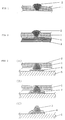
- Fig. 1 is shown an enlarged sectional view of one embodiment of the composite film according to the present invention.
- the composite film of the present invention comprises an insulating film 1 and a metallic material 2 which extends from the front to the back side of the insulating film 1 and projects from the insulating film 1 on one side thereof (upper side in the figure).
- the metallic material 2 in this composite film has a taper and is releasable from the insulating film 1. It is preferable that the taper of the metallic material 2 has an inclination such that the direction of the thickness of the insulating film 1 and the direction of the taper are at an angle of 20° or less, especially in the range of from 5 to 15°, to each other from the standpoint of releasability of the metallic material 2.
- That part of the metallic material 2 which projects from the insulating film 1 is not particularly limited in shape. However, it is preferable that in order to certainly bond and transfer the metallic material 2 to a semiconductor element, electric circuit, electric circuit part, or the like as an adherend, the projecting part has a mushroom shape as illustrated in the figure.
- the metallic material 2 comprises a solder, gold, silver, copper, nickel, tin, or an alloy of any of these metals. This metallic material 2 can also be utilized, for example, as a bump resistor.
- the insulating film 1 is made of a material having electrical insulating properties and appropriate heat resistance and flexibility.
- a material include various thermosetting resins and thermoplastic resins, such as polyester resins, epoxy resins, urethane resins, polystyrene resins, polyethylene resins, polyamide resins, polyimide resins, ABS (acrylonitrile-butadiene-styrene) resins, polycarbonate resins, silicone resins, and fluororesins.
- thermosetting resins and thermoplastic resins such as polyester resins, epoxy resins, urethane resins, polystyrene resins, polyethylene resins, polyamide resins, polyimide resins, ABS (acrylonitrile-butadiene-styrene) resins, polycarbonate resins, silicone resins, and fluororesins.
- transparent resins are preferred from the standpoint of easiness of positioning performed in transferred bump formation, while polyimide resins are preferred from the standpoints of heat resistance and mechanical
- the thickness of the insulating film 1 is arbitrarily selected according to the amount (volume) of a bump to be formed by transfer. However, from the standpoint of ensuring flexibility to the composite film, the thickness of the insulating film 1 is usually from 5 to 500 ⁇ m, preferably from 10 to 100 ⁇ m, more preferably from 15 to 40 ⁇ m.
- Fig. 2 is shown an enlarged sectional view of another preferred embodiment of the composite film according to the present invention.
- This composite film is provided with a pressure-sensitive sheet comprising a substrate 3 and a pressure-sensitive layer 4 on the insulating film 1 on the side of the taper head of the metallic material 2 (lower side in the figure). Due to this pressure-sensitive sheet, the metallic material 2 is prevented from falling off before use.
- the metallic material 2 is formed from a solder
- solder falling may be avoided by forming a metallic layer as a supporting layer on the insulating film 1 on one side thereof.
- This metallic layer preferably is made of a metal which does not melt and mingle with the solder when the solder is transferred by melting and which has poor wettability by the solder, in order to transfer the solder only.
- Solders usually are alloys of tin (Sn) and lead (Pb), and the component ratio of Sn/Pb varies according to the desired melting point. Exemplary ratios thereof are 90/10, 64/36, and 60/40 by weight.
- Fig. 3 are shown sectional views illustrating one embodiment of the transferred bump-forming method using the composite film shown in Fig. 1 according to the present invention.
- the projecting part of the metallic material 2 in the composite film of the present invention is bonded with an electrode part 6 on an external circuit 5 as an adherend.
- Fig. 4 are shown sectional views illustrating one embodiment of the solder bump-forming method using the composite film (in which the metallic material is a solder) shown in Fig. 1 according to the present invention.
- the projecting part of the solder 2 in the composite film of this invention is brought into contact with an electrode part 6 on, for example, an external circuit 5 as an adherend after or with positioning.
- an electrode part 6 on, for example, an external circuit 5 as an adherend after or with positioning.
- the surface of the electrode part 6 is previously covered with a metal (e.g., gold) having good wettability by the solder, because such a covering contributes to high-precision formation of a solder bump.
- the composite film of this invention is heated with a hot plate or a heating oven, upon which the solder 2 supported in the insulating film 1 melts and is transferred to the adherend (electrode part 6) to form a solder bump 2a (solder ball) of an almost spherical shape on the adherend as shown in Fig. 4 (B).
- the adherend electrode part 6
- solder bump 2a solder ball
- Fig. 5 are shown enlarged sectional views illustrating steps of a process for producing one embodiment of the composite film according to the present invention.
- a laminate comprising a conductor layer 8 which is a copper foil, copper sheet, or the like and an insulating film 1 formed on the conductor layer 8, as shown in Fig. 5 (A), is processed to form, in the insulating film 1, a hole 9 which extends to the conductor layer 8 as shown in Fig. 5 (B).
- Examples of the processing method for forming the hole 9 include mechanical processing, laser processing, light processing, and chemical etching. Of these, processing with an ultraviolet laser such as an excimer laser is preferred from the standpoint that by this processing, fine holes and holes with various shapes can be formed.
- Electrolytic plating is then conducted using the conductor layer 8 as an electrode, thereby to fill the hole 9 formed above with a metallic material 2 as shown in Fig. 5 (C).
- This plating for filling the hole 9 with the metallic material 2 is continued until the metallic material 2 being deposited comes to project from the surface of the insulating film 1.
- the shape and size of the projecting part of the metallic material 2 may suitably be determined according to the shape of a bump to be formed by transferring the metallic material 2 and the size of an electrode part as an adherend for the metallic material 2. However, it is preferable that from the standpoint of production precision and the like, the projecting part has a height up to about 5 times the radius of the hole, in the case that the hole has a circular cross section. Since the conductor layer 8 is removed in the subsequent step by etching, the metallic material 2 filling the hole 9 preferably is a metal which is different from the metal constituting the conductor layer 8 and has solubility different from that of the conductor layer 8.
- an alignment hole or a jig hole as described hereinabove may be formed by mechanical processing, laser processing, light processing, chemical etching, etc.
- Fig. 6 are shown enlarged sectional views illustrating steps of a process for producing another embodiment of the composite film according to the present invention.
- Fig. 6 (A) shows a three-layer sheet comprising a laminate of a conductor layer 8 with an insulating film 1 and, formed on the surface of the insulating film 1, a photoresist 10. In this photoresist 10, a desired photo-pattern is formed. As shown in Fig. 6 (B), a hole 9 is then formed in the exposed part of the insulating film 1 in the same manner as in the process illustrated in Fig. 5.
- electrolytic plating is conducted with the conductor layer 8 as an electrode to fill the hole 9 with a metallic material 2 and to allow the metallic material 2 to come to project from the insulating film 1 to form a projecting metallic material part surrounded by the photoresist 10 as shown in Fig. 6 (C).
- the conductor layer 8 is then removed by etching to obtain a composite film as shown in Fig. 6 (D). Due to the use of the photoresist 10 as in this process, the projecting part of the metallic material 2 can easily be designed to have an arbitrary shape.
- Figs. 7 to 9 are shown sectional views of other embodiments of the composite film according to the present invention.
- the composite film shown in Fig. 7 comprises an insulating film 1 and, supported therein, a metallic material 2 having a multilayer structure.
- This metallic material 2 has, on the surfaces thereof, metallic materials 11 and 12 having good bondability with adherends.
- Surface properties of the metallic material 2 can be modified by making the metallic material 2 to have such a multilayer structure.
- the composite film of the present invention is used for forming a transferred bump which is utilized as a junction point where a pressure is applied repeatedly or which should penetrate into an electrode part of an adherend, it is preferred to form the inner part of the metallic material 2 in Fig. 7 from a relatively hard metal such as nickel and to form the metallic materials 11 and 12, as surface layers required to have bondability with adherends, from gold or a solder.
- the composite film shown in Fig. 8 has a metallic material 2 which projects from both sides of an insulating film 1.
- the composite film shown in Fig. 9 has a metallic material 2 in which the inner part surrounded by an insulating film 1 has discontinuously changing diameters as shown in the figure.
- the metallic material 2 having a projecting part which projects from the lower-side surface of the insulating film 1 as in Figs. 8 and 9 can be obtained by conducting the same procedures as in the steps illustrated in Fig. 5 (B) to (D) except that before step (C), a surface layer of the exposed part of the conductor layer 8 is removed by etching with an etchant.
- the special shape of the inner part of the metallic material 2 in the composite film of Fig. 9 can be formed by conducting the same procedures as in the process illustrated in Fig. 5 except that the step of forming the hole 9 as shown in Fig. 5 (B) is performed in two stages.
- a transferred bump having an arbitrary shape according to the use of the bump can be formed.
- the composite film of this invention can be used to form a transferred bump which penetrates into and is bonded to an electrode part of an adherend or to form a solder ball-possessing check electrode for the inspection of semiconductor elements. It is also possible to form a needle-like transferred bump by making the hole 9 to have a needle shape.
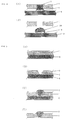
- Fig. 10 is shown a sectional view of one embodiment of the probe card structure according to the present invention.
- Numeral 16 denotes a probe card substrate.
- a desired check circuit pattern 13 and an electrode lead 14 are formed.
- a metallic material 2 is bonded by a heat-fusible bonding agent 15.
- each of the check circuit pattern 13 and the electrode lead 14 examples include electrically conductive materials such as various metals, e.g., gold, silver, copper, iron, nickel, and cobalt, and various alloys containing these metals as main components.
- the probe card structure of the present invention is produced, for example, as follows. First, an insulating resin is coated on a conductor layer 8 such as a metal foil and then heat-cured to form a probe card substrate 16, thereby preparing a two-layer sheet. The conductor layer 8 of the two-layer sheet is then subjected to an etching treatment by a conventional method to form a desired check circuit pattern 13 and an electrode lead 14, as shown in Fig. 11 (B), in order that the probe card structure produced can be used to test semiconductor devices for predetermined functions. Subsequently, a heat-fusible bonding agent 15, such as a solder, is coated on the surface of the electrode lead 14 as shown in Fig. 11 (C).
- a heat-fusible bonding agent 15 such as a solder
- the composite film of the present invention is then placed on the coated surface of the electrode lead 14 in a manner such that the metallic material 2 in the composite film comes into contact with the electrode lead 14. Thereafter, the heat-fusible bonding agent 15 is heated with or without application of pressure to bond the metallic material 2 to the electrode lead 14 as shown in Fig. 11 (D). After the metallic material 2 is bonded, only the insulating film 1 as a support for the metallic material 2 in the composite film is peeled off as shown in Fig. 11 (E). Thus, a probe card structure of the type shown in Fig. 10 is produced.
- the composite film used above which can be produced by the method described hereinabove, is not particularly limited in production method therefor and material thereof.
- the shape of the metallic material 2 is not limited to the bump shape with a flat head as shown in Fig. 10, and the metallic material 2 may be of a shape with a pointed head like the metallic material 2a shown in Fig. 12.
- a two-layer sheet was first prepared in the above-described process by coating an insulating resin on the conductor layer 8, it is possible to produce a two-layer sheet of the same structure by a method in which a probe card substrate 16 is previously prepared and a conductor layer 8 is formed on the insulating film 16, i.e., the probe card substrate, using an electrically conductive material by, for example, sputtering or any of various vapor deposition techniques and plating techniques.
- protective resin layers 17 are formed on the surfaces to which the metallic materials 2 are transferred, in order that during the electrical conduction inspection of semiconductor devices using the probe card structure of the present invention, shortcircuiting is avoided, the semiconductor devices is prevented from being damaged, and the metallic materials 2 is prevented from falling off.
- the thickness of the protective resin layers 17 is preferably from 1 to 50 ⁇ m, more preferably from 10 to 30 ⁇ m.
- the material for forming the protective resin layers 17 is not particularly limited, and examples thereof include thermosetting resins such as epoxy resins and thermoplastic resins such as fluororesins.
- the metallic materials 2 which are to be brought into direct contact with a semiconductor during inspection thereof are disposed in the desired parts of the structure due to the use of the composite film. Therefore, the probe card structure can be produced so as to have a predetermined shape without any particular limitation on the material and thickness thereof, and can be used for electrical conductivity inspections without causing any problem.
- An inspection of a semiconductor device using the probe card structure of the present invention may be conducted as follows. As shown in Fig. 14, metallic materials 2 of the probe card structure are brought into contact with electrode parts 6 in a semiconductor device 18 and electrical conductivity is then tested.
- a transferred bump can be formed from the metallic material with high precision and ease on an electrode part of a high-density semiconductor element or on an electrical part, electric circuit, or the like. Therefore, bump formation on semiconductor devices and other parts using the composite film of the present invention can be performed efficiently to attain a higher product yield and an improved production efficiency, as compared with the conventional bump connector technique in which a bump electrode is formed directly on a semiconductor device and this bump electrode is used as a junction point.
- the probe card structure of the present invention is produced by placing the composite film of this invention on an electrode lead formed on an insulating film in a manner such that the metallic bump in the composite film is placed in a predetermined position in the electrode lead surface, fixing the metallic bump to the electrode lead surface by heating, and then peeling only the base film of the composite film to transfer the metallic bump in the composite film to the electrode lead surface, the probe card structure is not limited in material and thickness thereof and can, hence, be easily made to have a desired checking ability. Therefore, when the probe card structure of the present invention is used for the inspection of semiconductors, occurrence of short-circuits between electrode leads can be avoided considerably and the semiconductor devices being inspected can be effectively prevented from suffering a damage. As a result, defective products resulting from semiconductor inspection can be diminished greatly.
Abstract
Description
- The present invention relates to a composite film which enables easy formation of a bump for use in an electrical connection or as a junction point in semiconductor elements, electric parts, electric circuits, and the like, a method of forming a transferred bump using the film, a probe card structure obtained using the film, and a process for producing the probe card structure using the film and the transferred bump-forming method.
- With the recent growth of the semiconductor industry, thickness reduction and size and weight reduction in electronic machines and instruments have been proceeding and, in the production of machines and instruments employing a large number of semiconductor devices, there is a desire to mount semiconductor elements on a certain area of a substrate at a high density. According to the present-day technique for semiconductor mounting, metallic bumps are formed on a semiconductor element directly or by transfer and this semiconductor element is mounted using the bumps as connecting terminals. If a method of forming such bumps can be applied to various kinds of electrical and electronic parts other than semiconductor elements, this leads to an improvement in mounting density in electronic machines and instruments.
- Actually however, direct formation of a bump on semiconductor elements and on many kinds of other electrical and electronic parts, in general, is technically difficult and may result in a decrease in yield. On the other hand, a method of forming a bump by transfer, or a method of forming a transferred bump, has been proposed. However, the currently employed transfer method in which a bump is formed on an ITO (indium tin oxide) electrode-possessing glass has various limitations on production cost, production process, bump transfer method, etc., and is hence unsatisfactory from the standpoint of practical use thereof.
- In particular, in the field of various functional parts employed in OA machines and instruments, improvements of size-reduction techniques including surface mounting are being hastened. As a result, the demand for higher mounting densities is becoming severe and mounting with a terminal pitch of 0.3 mm or less has come to be desired.
- However, such high mounting densities have been difficult to attain by the ordinary technique in which bumps formed from a solder paste by printing or the like are used as connecting terminals for mounting, because according to this technique, smaller terminal pitches result in a higher possibility of formation of a solder bridge between printed solder bumps and in lower reliability of electrical connection. The printing method has another drawback that the amount of solder printed fluctuates considerably, so that it is difficult to form solder bumps with high precision.
- Further, in surface mounting for electric circuits, chip-fixed resistors of a rectangular or circular shape are, for example, being used. However, the attainable size reduction in such chip-fixed resistors to be subjected to surface mounting is limited and, in addition, there are problems that the mounting requires soldering by hand or in a similar way and that positioning for mounting is difficult.
- With the recent trend toward thickness reduction and size and weight reduction in electronic machines and instruments, the degree of semiconductor integration and the density of semiconductor mounting are increasing. With the progress of these, the number of electrodes in a single semiconductor device is increasing and electrode pitches in semiconductor devices are also becoming smaller year by year. Moreover, there also is a desire for a technique for checking semiconductor devices for the purpose of direct mounting of bare chips on circuit substrates or for other purposes. Although needle-type mechanical probes are usually used in the inspection of semiconductor devices, such mechanical probes, especially high-density mechanical probes, have service lives as short as from 10,000 to 20,000 times in terms of number of contacts and they also have a drawback that the relative position of needles and blades interposed between the needles readily shifts and the needles and blades often bend or, in some cases, cause a short-circuit. In addition, there are cases that since to connect a mechanical probe with a semiconductor device necessitates a force which presses the probe against the semiconductor device, needles and blades of the probe stick into the die pad of the semiconductor device to damage it and the inspection thus yields defective products. The mechanical probes moreover have a drawback that it is difficult to employ a complicated structure because impedance matching by means of needles is difficult.
- As an expedient for overcoming these problems, a semiconductor-checking device obtained by forming minute holes in a base plate and filling the minute holes with an electrically conductive material to form electrically conductive paths has, for example, been proposed (JP-A-3-293566). (The term "JP-A" as used herein means an "unexamined published Japanese patent application".) Such semiconductor-checking devices, however, have restrictions on the material and thickness of the base plate because of the construction thereof. Illustratively stated, there are cases that a plate to be used as the base plate is made of a material unsuitable for selective etching for forming minute holes or has a thickness which is so large that formation of minute holes in the plate is virtually impossible. Therefore, in order to produce a semiconductor-checking device having a desired structure, the thickness of the base plate is limited considerably and, as a result, the mechanical strength of the thus-obtained semiconductor-checking device itself is also limited. Even if the checking device can be produced without any limitation on the base plate, the production process is not easy.
- The present inventors have conducted intensive studies to overcome the above-described problems. As a result, it has been found that a transferred bump can be formed easily when an insulating film of a specific structure in which a metallic material for forming a bump is held in a releasable state is used. The present invention has been completed based on this finding.
- An object of the present invention is to provide a composite film which can be used for establishing an electrical connection or forming a junction point, with ease and high precision, in semiconductor elements, electrical and electronic parts, electric circuits, and the like.
- Another object of the present invention is to provide a transferred bump-forming method using the above-described film.
- Still another object of the present invention is to provide a probe card structure obtained using the above-described film.
- A further object of the present invention is to provide a process for producing the probe card structure using the above-described film and the transferred bump-forming method.
- The composite film according to the present invention comprises an insulating film and a metallic material extending from the front to the back side of the insulating film through a through-hole formed in the insulating film, the metallic material projecting from the insulating film on at least one side thereof and being releasable from the insulating film.
- The method of forming a transferred bump according to the present invention comprises bringing the composite film described above into contact with a semiconductor element, an electric circuit, or an electric circuit part as an adherend and then peeling the insulating film only, with the metallic material being left on the adherend at the contact site.
- The probe card structure according to the present invention comprises an insulating film, a predetermined check circuit pattern formed on the insulating film, an electrode lead formed on the insulating film, and a bump-shape metallic material bonded to the electrode lead surface.
- The process for fabricating a probe card structure according to the present invention comprises the steps of forming a predetermined check circuit pattern and an electrode lead on a surface of a probe card substrate, forming a layer of a heat-fusible bonding agent on the surface of the electrode lead, preparing the composite film described above, placing the composite film on the electrode lead so that the metallic material of the composite film comes to be in a predetermined position in the surface of the electrode lead, heating the heat-fusible bonding agent on the electrode lead thereby to fix the composite film on the electrode lead surface, and peeling only the insulating film of the composite film thereby to transfer the metallic material to the electrode lead surface.
- Fig. 1 is an enlarged sectional view of one embodiment of the composite film according to the present invention.
- Fig. 2 is an enlarged sectional view of another embodiment of the composite film according to the present invention.
- Fig. 3 (A) to (C) are enlarged sectional views illustrating one embodiment of the transferred bump-forming method using the composite film shown in Fig. 1 according to the present invention.
- Fig. 4 (A) and (B) are enlarged sectional views illustrating another embodiment of the transferred bump-forming method using the composite film shown in Fig. 1 according to the present invention.
- Fig. 5 (A) to (D) are enlarged sectional views illustrating steps of a process for producing one embodiment of the composite film according to the present invention.
- Fig. 6 (A) to (D) are enlarged sectional views illustrating steps of a process for producing another embodiment of the composite film according to the present invention.
- Fig. 7 is an enlarged sectional view of still another embodiment of the composite film according to the present invention.
- Fig. 8 is an enlarged sectional view of a further embodiment of the composite film according to the present invention.
- Fig. 9 is an enlarged sectional view of still a further embodiment of the composite film according to the present invention.
- Fig. 10 is a sectional view of one embodiment of the probe card structure according to the present invention.
- Fig. 11 (A) to (F) are views illustrating steps of a process for fabricating one embodiment of the probe card structure according to the present invention.
- Fig. 12 is a partial sectional view of the main part of another embodiment of the probe card structure according to the present invention, the view showing another example of the metallic material.
- Fig. 13 is a sectional view of still another embodiment of the probe card structure according to the present invention.
- Fig. 14 is a view illustrating electrical conduction inspection of a semiconductor device using the probe card structure according to the present invention.
-
- The composite film and the transferred bump-forming method using the film, according to the present invention, are explained below with reference to accompanying drawings.
- In Fig. 1 is shown an enlarged sectional view of one embodiment of the composite film according to the present invention.
- As is apparent from Fig. 1, the composite film of the present invention comprises an
insulating film 1 and ametallic material 2 which extends from the front to the back side of theinsulating film 1 and projects from theinsulating film 1 on one side thereof (upper side in the figure). Themetallic material 2 in this composite film has a taper and is releasable from theinsulating film 1. It is preferable that the taper of themetallic material 2 has an inclination such that the direction of the thickness of theinsulating film 1 and the direction of the taper are at an angle of 20° or less, especially in the range of from 5 to 15°, to each other from the standpoint of releasability of themetallic material 2. That part of themetallic material 2 which projects from theinsulating film 1 is not particularly limited in shape. However, it is preferable that in order to certainly bond and transfer themetallic material 2 to a semiconductor element, electric circuit, electric circuit part, or the like as an adherend, the projecting part has a mushroom shape as illustrated in the figure. - The
metallic material 2 comprises a solder, gold, silver, copper, nickel, tin, or an alloy of any of these metals. Thismetallic material 2 can also be utilized, for example, as a bump resistor. - The
insulating film 1 is made of a material having electrical insulating properties and appropriate heat resistance and flexibility. Examples of such a material include various thermosetting resins and thermoplastic resins, such as polyester resins, epoxy resins, urethane resins, polystyrene resins, polyethylene resins, polyamide resins, polyimide resins, ABS (acrylonitrile-butadiene-styrene) resins, polycarbonate resins, silicone resins, and fluororesins. Of these resins, transparent resins are preferred from the standpoint of easiness of positioning performed in transferred bump formation, while polyimide resins are preferred from the standpoints of heat resistance and mechanical strength. - The thickness of the insulating
film 1 is arbitrarily selected according to the amount (volume) of a bump to be formed by transfer. However, from the standpoint of ensuring flexibility to the composite film, the thickness of the insulatingfilm 1 is usually from 5 to 500 µm, preferably from 10 to 100 µm, more preferably from 15 to 40 µm. - In Fig. 2 is shown an enlarged sectional view of another preferred embodiment of the composite film according to the present invention. This composite film is provided with a pressure-sensitive sheet comprising a
substrate 3 and a pressure-sensitive layer 4 on the insulatingfilm 1 on the side of the taper head of the metallic material 2 (lower side in the figure). Due to this pressure-sensitive sheet, themetallic material 2 is prevented from falling off before use. Where themetallic material 2 is formed from a solder, it is possible to form themetallic material 2 by filling the through-hole in the insulatingfilm 1 with a solder in a manner such that the solder comes to project from both of the front and back sides of the insulatingfilm 1 with each projecting part being made to have a rivet head-like shape, thereby preventing the solder from falling off before use. Alternatively, solder falling may be avoided by forming a metallic layer as a supporting layer on the insulatingfilm 1 on one side thereof. This metallic layer preferably is made of a metal which does not melt and mingle with the solder when the solder is transferred by melting and which has poor wettability by the solder, in order to transfer the solder only. Examples of such a metal include nickel and chromium. Solders usually are alloys of tin (Sn) and lead (Pb), and the component ratio of Sn/Pb varies according to the desired melting point. Exemplary ratios thereof are 90/10, 64/36, and 60/40 by weight. - In Fig. 3 are shown sectional views illustrating one embodiment of the transferred bump-forming method using the composite film shown in Fig. 1 according to the present invention.
- As illustrated in Fig. 3 (A), the projecting part of the
metallic material 2 in the composite film of the present invention is bonded with anelectrode part 6 on anexternal circuit 5 as an adherend. In order to perform precise positioning in this bonding step, it is preferred to form an alignment hole or a jig hole beforehand in the composite film of this invention. Further, it is advantageous to previously form a layer of ametal 7 which readily melts upon heating, such as a solder, on the surface of theelectrode part 6, because when themetallic material 2 is made of a metal, e.g., gold, having good wettability by solder, themetallic material 2 can be easily bonded with theelectrode part 6, as shown in Fig. 3 (B), by only heating themetal 7 while themetallic material 2 is kept in contact with themetal 7 with or without application of pressure. After bonding, only the insulatingfilm 1 is peeled off, whereby only themetallic material 2 can be transferred to theelectrode part 6 as shown in Fig. 3 (C). Even in the case of using a semiconductor element as an adherend in place of theexternal circuit 5, the same procedures as described above may be conducted to form a transferred bump. - In Fig. 4 are shown sectional views illustrating one embodiment of the solder bump-forming method using the composite film (in which the metallic material is a solder) shown in Fig. 1 according to the present invention.
- As shown in Fig. 4 (A), the projecting part of the
solder 2 in the composite film of this invention is brought into contact with anelectrode part 6 on, for example, anexternal circuit 5 as an adherend after or with positioning. In order to conduct this positioning precisely, it is preferred to form an alignment hole or a jig hole beforehand in the composite film of the present invention. It is also preferable that the surface of theelectrode part 6 is previously covered with a metal (e.g., gold) having good wettability by the solder, because such a covering contributes to high-precision formation of a solder bump. Subsequently, the composite film of this invention is heated with a hot plate or a heating oven, upon which thesolder 2 supported in the insulatingfilm 1 melts and is transferred to the adherend (electrode part 6) to form a solder bump 2a (solder ball) of an almost spherical shape on the adherend as shown in Fig. 4 (B). Even in the case of using a semiconductor element as an adherend in place of theexternal circuit 5, the same procedures as described above may be conducted to form a solder bump. - In Fig. 5 are shown enlarged sectional views illustrating steps of a process for producing one embodiment of the composite film according to the present invention.
- A laminate comprising a
conductor layer 8 which is a copper foil, copper sheet, or the like and an insulatingfilm 1 formed on theconductor layer 8, as shown in Fig. 5 (A), is processed to form, in the insulatingfilm 1, ahole 9 which extends to theconductor layer 8 as shown in Fig. 5 (B). Examples of the processing method for forming thehole 9 include mechanical processing, laser processing, light processing, and chemical etching. Of these, processing with an ultraviolet laser such as an excimer laser is preferred from the standpoint that by this processing, fine holes and holes with various shapes can be formed. - Electrolytic plating is then conducted using the
conductor layer 8 as an electrode, thereby to fill thehole 9 formed above with ametallic material 2 as shown in Fig. 5 (C). This plating for filling thehole 9 with themetallic material 2 is continued until themetallic material 2 being deposited comes to project from the surface of the insulatingfilm 1. The shape and size of the projecting part of themetallic material 2 may suitably be determined according to the shape of a bump to be formed by transferring themetallic material 2 and the size of an electrode part as an adherend for themetallic material 2. However, it is preferable that from the standpoint of production precision and the like, the projecting part has a height up to about 5 times the radius of the hole, in the case that the hole has a circular cross section. Since theconductor layer 8 is removed in the subsequent step by etching, themetallic material 2 filling thehole 9 preferably is a metal which is different from the metal constituting theconductor layer 8 and has solubility different from that of theconductor layer 8. - Finally, the
conductor layer 8 is removed by a known etching treatment to obtain a composite film according to the present invention as shown in Fig. 5 (D). In the composite film thus obtained, an alignment hole or a jig hole as described hereinabove may be formed by mechanical processing, laser processing, light processing, chemical etching, etc. - In Fig. 6 are shown enlarged sectional views illustrating steps of a process for producing another embodiment of the composite film according to the present invention.
- Fig. 6 (A) shows a three-layer sheet comprising a laminate of a
conductor layer 8 with an insulatingfilm 1 and, formed on the surface of the insulatingfilm 1, aphotoresist 10. In thisphotoresist 10, a desired photo-pattern is formed. As shown in Fig. 6 (B), ahole 9 is then formed in the exposed part of the insulatingfilm 1 in the same manner as in the process illustrated in Fig. 5. - Subsequently, electrolytic plating is conducted with the
conductor layer 8 as an electrode to fill thehole 9 with ametallic material 2 and to allow themetallic material 2 to come to project from the insulatingfilm 1 to form a projecting metallic material part surrounded by thephotoresist 10 as shown in Fig. 6 (C). Theconductor layer 8 is then removed by etching to obtain a composite film as shown in Fig. 6 (D). Due to the use of thephotoresist 10 as in this process, the projecting part of themetallic material 2 can easily be designed to have an arbitrary shape. - In Figs. 7 to 9 are shown sectional views of other embodiments of the composite film according to the present invention.
- The composite film shown in Fig. 7 comprises an insulating
film 1 and, supported therein, ametallic material 2 having a multilayer structure. Thismetallic material 2 has, on the surfaces thereof,metallic materials metallic material 2 can be modified by making themetallic material 2 to have such a multilayer structure. For example, where the composite film of the present invention is used for forming a transferred bump which is utilized as a junction point where a pressure is applied repeatedly or which should penetrate into an electrode part of an adherend, it is preferred to form the inner part of themetallic material 2 in Fig. 7 from a relatively hard metal such as nickel and to form themetallic materials - The composite film shown in Fig. 8 has a
metallic material 2 which projects from both sides of an insulatingfilm 1. The composite film shown in Fig. 9 has ametallic material 2 in which the inner part surrounded by an insulatingfilm 1 has discontinuously changing diameters as shown in the figure. Themetallic material 2 having a projecting part which projects from the lower-side surface of the insulatingfilm 1 as in Figs. 8 and 9 can be obtained by conducting the same procedures as in the steps illustrated in Fig. 5 (B) to (D) except that before step (C), a surface layer of the exposed part of theconductor layer 8 is removed by etching with an etchant. - The special shape of the inner part of the
metallic material 2 in the composite film of Fig. 9 can be formed by conducting the same procedures as in the process illustrated in Fig. 5 except that the step of forming thehole 9 as shown in Fig. 5 (B) is performed in two stages. - As described above, by use of the composite film of the present invention, a transferred bump having an arbitrary shape according to the use of the bump can be formed. For example, the composite film of this invention can be used to form a transferred bump which penetrates into and is bonded to an electrode part of an adherend or to form a solder ball-possessing check electrode for the inspection of semiconductor elements. It is also possible to form a needle-like transferred bump by making the
hole 9 to have a needle shape. - The probe card structure and the production process thereof according to the present invention are explained below with reference to accompanying drawings.
- In Fig. 10 is shown a sectional view of one embodiment of the probe card structure according to the present invention.
Numeral 16 denotes a probe card substrate. On one side of theprobe card substrate 16, a desiredcheck circuit pattern 13 and anelectrode lead 14 are formed. To theelectrode lead 14, ametallic material 2 is bonded by a heat-fusible bonding agent 15. - Examples of the material of each of the
check circuit pattern 13 and theelectrode lead 14 include electrically conductive materials such as various metals, e.g., gold, silver, copper, iron, nickel, and cobalt, and various alloys containing these metals as main components. - The probe card structure of the present invention is produced, for example, as follows. First, an insulating resin is coated on a
conductor layer 8 such as a metal foil and then heat-cured to form aprobe card substrate 16, thereby preparing a two-layer sheet. Theconductor layer 8 of the two-layer sheet is then subjected to an etching treatment by a conventional method to form a desiredcheck circuit pattern 13 and anelectrode lead 14, as shown in Fig. 11 (B), in order that the probe card structure produced can be used to test semiconductor devices for predetermined functions. Subsequently, a heat-fusible bonding agent 15, such as a solder, is coated on the surface of theelectrode lead 14 as shown in Fig. 11 (C). The composite film of the present invention is then placed on the coated surface of theelectrode lead 14 in a manner such that themetallic material 2 in the composite film comes into contact with theelectrode lead 14. Thereafter, the heat-fusible bonding agent 15 is heated with or without application of pressure to bond themetallic material 2 to theelectrode lead 14 as shown in Fig. 11 (D). After themetallic material 2 is bonded, only the insulatingfilm 1 as a support for themetallic material 2 in the composite film is peeled off as shown in Fig. 11 (E). Thus, a probe card structure of the type shown in Fig. 10 is produced. - The composite film used above, which can be produced by the method described hereinabove, is not particularly limited in production method therefor and material thereof. Further, the shape of the
metallic material 2 is not limited to the bump shape with a flat head as shown in Fig. 10, and themetallic material 2 may be of a shape with a pointed head like the metallic material 2a shown in Fig. 12. - Although a two-layer sheet was first prepared in the above-described process by coating an insulating resin on the
conductor layer 8, it is possible to produce a two-layer sheet of the same structure by a method in which aprobe card substrate 16 is previously prepared and aconductor layer 8 is formed on the insulatingfilm 16, i.e., the probe card substrate, using an electrically conductive material by, for example, sputtering or any of various vapor deposition techniques and plating techniques. - It is preferable that, as shown in Fig. 13, protective resin layers 17 are formed on the surfaces to which the
metallic materials 2 are transferred, in order that during the electrical conduction inspection of semiconductor devices using the probe card structure of the present invention, shortcircuiting is avoided, the semiconductor devices is prevented from being damaged, and themetallic materials 2 is prevented from falling off. The thickness of the protective resin layers 17 is preferably from 1 to 50 µm, more preferably from 10 to 30 µm. The material for forming the protective resin layers 17 is not particularly limited, and examples thereof include thermosetting resins such as epoxy resins and thermoplastic resins such as fluororesins. - In the probe card structure thus obtained, the
metallic materials 2 which are to be brought into direct contact with a semiconductor during inspection thereof are disposed in the desired parts of the structure due to the use of the composite film. Therefore, the probe card structure can be produced so as to have a predetermined shape without any particular limitation on the material and thickness thereof, and can be used for electrical conductivity inspections without causing any problem. - An inspection of a semiconductor device using the probe card structure of the present invention may be conducted as follows. As shown in Fig. 14,
metallic materials 2 of the probe card structure are brought into contact withelectrode parts 6 in asemiconductor device 18 and electrical conductivity is then tested. - As described above, since a bump-forming metallic material of a desired size is releasably contained in the composite film of the present invention, a transferred bump can be formed from the metallic material with high precision and ease on an electrode part of a high-density semiconductor element or on an electrical part, electric circuit, or the like. Therefore, bump formation on semiconductor devices and other parts using the composite film of the present invention can be performed efficiently to attain a higher product yield and an improved production efficiency, as compared with the conventional bump connector technique in which a bump electrode is formed directly on a semiconductor device and this bump electrode is used as a junction point.
- Furthermore, since the probe card structure of the present invention is produced by placing the composite film of this invention on an electrode lead formed on an insulating film in a manner such that the metallic bump in the composite film is placed in a predetermined position in the electrode lead surface, fixing the metallic bump to the electrode lead surface by heating, and then peeling only the base film of the composite film to transfer the metallic bump in the composite film to the electrode lead surface, the probe card structure is not limited in material and thickness thereof and can, hence, be easily made to have a desired checking ability. Therefore, when the probe card structure of the present invention is used for the inspection of semiconductors, occurrence of short-circuits between electrode leads can be avoided considerably and the semiconductor devices being inspected can be effectively prevented from suffering a damage. As a result, defective products resulting from semiconductor inspection can be diminished greatly.
- While the invention has been described in detail and with reference to specific embodiments thereof, it will be apparent to one skilled in the art that various changes and modifications can be made therein without departing from the spirit and scope thereof.
Claims (14)
- A composite film comprising an insulating film and a metallic material extending from the front to the back side of the insulating film through a through-hole formed in the insulating film, said metallic material projecting from the insulating film on at least one side thereof and being releasable from the insulating film.
- A composite film as claimed in claim 1, wherein the metallic material is a solder and can be released from the insulating film by melting.
- A composite film as claimed in claim 1, wherein the metallic material is a bump resistor.
- A composite film as claimed in claim 1, wherein the metallic material which fills the through-hole in the insulating film has a taper.
- A composite film as claimed in claim 4, wherein the direction of the thickness of the insulating film and the direction of the taper of the metallic material are at an angle of 20° or less.
- A composite film as claimed in claim 1, wherein the projecting part of the metallic material is of a mushroom shape.
- A composite film as claimed in claim 4, wherein a pressure-sensitive sheet is bonded to the insulating film surface on the taper head side of the metallic material.
- A composite film as claimed in claim 1, wherein the through-hole through which the metallic material extends is formed by irradiation with a laser light.
- A method of forming a transferred bump which comprises bringing the composite film as claimed in claim 1 into contact with a semiconductor element, an electric circuit, or an electric circuit part and then peeling the insulating film only, with the metallic material being left on the semiconductor element, electric circuit, or electric circuit part at the contact site.
- A method as claimed in claim 9, which comprises bringing the composite film in which the metallic material is a solder into contact with a semiconductor element, an electric circuit, or an electric circuit part and then heating and melting the solder to transfer the solder to the contact site.
- A method as claimed in claim 9, wherein the metallic material is a bump resistor.
- A probe card structure which comprises an insulating film, a predetermined check circuit pattern formed on the insulating film, an electrode lead formed on the insulating film, and a bump-shape metallic material bonded to the electrode lead surface.
- A probe card structure as claimed in claim 12, which further comprises a protective resin layer formed on the surface to which the bump-shaped metallic material is bonded.
- A process for producing a probe card structure which comprises the steps of forming a predetermined check circuit pattern and an electrode lead on a surface of an insulating film, forming a layer of a heat-fusible bonding agent on the surface of the electrode lead, preparing the composite film as claimed in claim 1, placing the composite film on the electrode lead so that the metallic material of the composite film comes to be in a predetermined position in the surface of the electrode lead, heating the heat-fusible bonding agent on the electrode lead to fix the composite film on the electrode lead surface, and peeling only the insulating film of the composite film to transfer the metallic material to the electrode lead surface.
Applications Claiming Priority (10)
| Application Number | Priority Date | Filing Date | Title |
|---|---|---|---|
| JP340384/91 | 1991-11-28 | ||
| JP34038491 | 1991-11-28 | ||
| JP5753692A JPH05226430A (en) | 1992-02-10 | 1992-02-10 | Probe card body structure and manufacturing method thereof |
| JP57536/92 | 1992-02-10 | ||
| JP61228/92 | 1992-02-14 | ||
| JP4061228A JPH05226101A (en) | 1992-02-14 | 1992-02-14 | Bump resistor-mounting film and bump resistor-mounting method |
| JP87942/92 | 1992-03-11 | ||
| JP8794292A JPH05206143A (en) | 1991-11-28 | 1992-03-11 | Composite film, and formation of transfer bump by use thereof |
| JP4152849A JPH05326526A (en) | 1992-05-19 | 1992-05-19 | Composite film and formation of solder bump using the same |
| JP152849/92 | 1992-05-19 |
Publications (2)
| Publication Number | Publication Date |
|---|---|
| EP0544305A2 true EP0544305A2 (en) | 1993-06-02 |
| EP0544305A3 EP0544305A3 (en) | 1993-10-06 |
Family
ID=27523375
Family Applications (1)
| Application Number | Title | Priority Date | Filing Date |
|---|---|---|---|
| EP19920120222 Withdrawn EP0544305A3 (en) | 1991-11-28 | 1992-11-26 | Method of forming a contact bump using a composite film |
Country Status (1)
| Country | Link |
|---|---|
| EP (1) | EP0544305A3 (en) |
Cited By (9)
| Publication number | Priority date | Publication date | Assignee | Title |
|---|---|---|---|---|
| WO1997031395A1 (en) * | 1996-02-23 | 1997-08-28 | Siemens Aktiengesellschaft | Method of producing bumps on pads of electronic components |
| EP0792463A1 (en) * | 1994-11-15 | 1997-09-03 | Formfactor, Inc. | Mounting spring elements on semiconductor devices, and wafer-level testing methodology |
| EP0859686A1 (en) * | 1995-05-26 | 1998-08-26 | Formfactor, Inc. | Fabricating interconnects and tips using sacrificial substrates |
| US5877559A (en) * | 1995-06-12 | 1999-03-02 | Nitto Denko Corporation | Film carrier for fine-pitched and high density mounting and semiconductor device using same |
| US6222272B1 (en) | 1996-08-06 | 2001-04-24 | Nitto Denko Corporation | Film carrier and semiconductor device using same |
| US6624648B2 (en) | 1993-11-16 | 2003-09-23 | Formfactor, Inc. | Probe card assembly |
| US6759258B2 (en) | 1997-05-09 | 2004-07-06 | Renesas Technology Corp. | Connection device and test system |
| EP1610375A2 (en) * | 1995-05-26 | 2005-12-28 | FormFactor, Inc. | Contact carriers for populating substrates with spring contacts |
| US9476911B2 (en) | 2004-05-21 | 2016-10-25 | Microprobe, Inc. | Probes with high current carrying capability and laser machining methods |
Families Citing this family (4)
| Publication number | Priority date | Publication date | Assignee | Title |
|---|---|---|---|---|
| US6741085B1 (en) | 1993-11-16 | 2004-05-25 | Formfactor, Inc. | Contact carriers (tiles) for populating larger substrates with spring contacts |
| US20020053734A1 (en) | 1993-11-16 | 2002-05-09 | Formfactor, Inc. | Probe card assembly and kit, and methods of making same |
| US8033838B2 (en) | 1996-02-21 | 2011-10-11 | Formfactor, Inc. | Microelectronic contact structure |
| US8988091B2 (en) | 2004-05-21 | 2015-03-24 | Microprobe, Inc. | Multiple contact probes |
Citations (1)
| Publication number | Priority date | Publication date | Assignee | Title |
|---|---|---|---|---|
| US5090118A (en) * | 1990-07-31 | 1992-02-25 | Texas Instruments Incorporated | High performance test head and method of making |
-
1992
- 1992-11-26 EP EP19920120222 patent/EP0544305A3/en not_active Withdrawn
Patent Citations (1)
| Publication number | Priority date | Publication date | Assignee | Title |
|---|---|---|---|---|
| US5090118A (en) * | 1990-07-31 | 1992-02-25 | Texas Instruments Incorporated | High performance test head and method of making |
Non-Patent Citations (3)
| Title |
|---|
| IBM TECHNICAL DISCLOSURE BULLETIN. vol. 29, no. 9, February 1987, NEW YORK US pages 3817 - 3818 'Placing Solder Terminals on Silicon Wafers' * |
| PATENT ABSTRACTS OF JAPAN vol. 12, no. 20 (E-575)21 January 1988 & JP-A-62 177 935 ( TOSHIBA CORP. ) * |
| RESEARCH DISCLOSURE no. 326, June 1991, HAVANT GB page 404 'Decal Contactor with Decoder' abstr.nr. 32 636 * |
Cited By (14)
| Publication number | Priority date | Publication date | Assignee | Title |
|---|---|---|---|---|
| US6624648B2 (en) | 1993-11-16 | 2003-09-23 | Formfactor, Inc. | Probe card assembly |
| EP0792463A1 (en) * | 1994-11-15 | 1997-09-03 | Formfactor, Inc. | Mounting spring elements on semiconductor devices, and wafer-level testing methodology |
| EP0792463A4 (en) * | 1994-11-15 | 1998-06-24 | Formfactor Inc | Mounting spring elements on semiconductor devices, and wafer-level testing methodology |
| EP1610375A2 (en) * | 1995-05-26 | 2005-12-28 | FormFactor, Inc. | Contact carriers for populating substrates with spring contacts |
| EP0859686A4 (en) * | 1995-05-26 | 1998-11-11 | Formfactor Inc | Fabricating interconnects and tips using sacrificial substrates |
| EP0859686A1 (en) * | 1995-05-26 | 1998-08-26 | Formfactor, Inc. | Fabricating interconnects and tips using sacrificial substrates |
| EP1610375A3 (en) * | 1995-05-26 | 2008-11-05 | FormFactor, Inc. | Contact carriers for populating substrates with spring contacts |
| US5877559A (en) * | 1995-06-12 | 1999-03-02 | Nitto Denko Corporation | Film carrier for fine-pitched and high density mounting and semiconductor device using same |
| WO1997031395A1 (en) * | 1996-02-23 | 1997-08-28 | Siemens Aktiengesellschaft | Method of producing bumps on pads of electronic components |
| US6222272B1 (en) | 1996-08-06 | 2001-04-24 | Nitto Denko Corporation | Film carrier and semiconductor device using same |
| US6759258B2 (en) | 1997-05-09 | 2004-07-06 | Renesas Technology Corp. | Connection device and test system |
| US7285430B2 (en) | 1997-05-09 | 2007-10-23 | Hitachi, Ltd. | Connection device and test system |
| US7541202B2 (en) | 1997-05-09 | 2009-06-02 | Renesas Technology Corp. | Connection device and test system |
| US9476911B2 (en) | 2004-05-21 | 2016-10-25 | Microprobe, Inc. | Probes with high current carrying capability and laser machining methods |
Also Published As
| Publication number | Publication date |
|---|---|
| EP0544305A3 (en) | 1993-10-06 |
Similar Documents
| Publication | Publication Date | Title |
|---|---|---|
| CA1259425A (en) | Balltape structure for tape automated bonding, multilayer packaging, universal chip interconnection and energy beam processes for manufacturing balltape | |
| JP2664873B2 (en) | Electronic package and manufacturing method thereof | |
| US6420664B1 (en) | Metal foil having bumps, circuit substrate having the metal foil, and semiconductor device having the circuit substrate | |
| KR100272156B1 (en) | Wiring sheet assemblies and forming electrical connections thereof | |
| JP2892505B2 (en) | Mounting electronic components on circuit boards | |
| JP2702507B2 (en) | Electrical connection member and method of manufacturing the same | |
| US6331679B1 (en) | Multi-layer circuit board using anisotropic electro-conductive adhesive layer | |
| KR100466680B1 (en) | Thin film attachment to laminate using a dendritic interconnection | |
| US5245750A (en) | Method of connecting a spaced ic chip to a conductor and the article thereby obtained | |
| JP2001102734A (en) | Multilayer flexible wiring board | |
| EP0544305A2 (en) | Method of forming a contact bump using a composite film | |
| KR20010042782A (en) | Semiconductor device, circuit board, method of manufacturing circuit board, and electronic device | |
| JP2004193334A (en) | Bump-forming sheet, and its manufacturing method | |
| EP0327399A1 (en) | Method of manufacturing an uniaxially electrically conductive article | |
| US5883432A (en) | Connection structure between electrode pad on semiconductor device and printed pattern on printed circuit board | |
| JPH03178152A (en) | Molded ic and its manufacture | |
| US9673063B2 (en) | Terminations | |
| JPH05226430A (en) | Probe card body structure and manufacturing method thereof | |
| JPH03129745A (en) | Mounting of semiconductor device | |
| JPH05206143A (en) | Composite film, and formation of transfer bump by use thereof | |
| JP2785832B2 (en) | Semiconductor device mounting structure | |
| US11432402B2 (en) | Flipped-conductor-patch lamination for ultra fine-line substrate creation | |
| JP3553246B2 (en) | Method of manufacturing IC module for IC card and method of manufacturing IC module | |
| JP2000340594A (en) | Transfer bump sheet and manufacture thereof | |
| JPH11312758A (en) | Manufacture of solder bump sheet and ic package component |
Legal Events
| Date | Code | Title | Description |
|---|---|---|---|
| PUAI | Public reference made under article 153(3) epc to a published international application that has entered the european phase |
Free format text: ORIGINAL CODE: 0009012 |
|
| AK | Designated contracting states |
Kind code of ref document: A2 Designated state(s): DE FR GB NL |
|
| PUAL | Search report despatched |
Free format text: ORIGINAL CODE: 0009013 |
|
| AK | Designated contracting states |
Kind code of ref document: A3 Designated state(s): DE FR GB NL |
|
| 17P | Request for examination filed |
Effective date: 19931222 |
|
| 17Q | First examination report despatched |
Effective date: 19950601 |
|
| STAA | Information on the status of an ep patent application or granted ep patent |
Free format text: STATUS: THE APPLICATION IS DEEMED TO BE WITHDRAWN |
|
| 18D | Application deemed to be withdrawn |
Effective date: 19980129 |