EP3496300B1 - Integriertes schaltungspaket mit elektrooptischer verbindungsschaltung - Google Patents
Integriertes schaltungspaket mit elektrooptischer verbindungsschaltung Download PDFInfo
- Publication number
- EP3496300B1 EP3496300B1 EP18204765.4A EP18204765A EP3496300B1 EP 3496300 B1 EP3496300 B1 EP 3496300B1 EP 18204765 A EP18204765 A EP 18204765A EP 3496300 B1 EP3496300 B1 EP 3496300B1
- Authority
- EP
- European Patent Office
- Prior art keywords
- die
- optical engine
- transceiver
- optical
- integrated circuit
- Prior art date
- Legal status (The legal status is an assumption and is not a legal conclusion. Google has not performed a legal analysis and makes no representation as to the accuracy of the status listed.)
- Active
Links
Images




Classifications
-
- G—PHYSICS
- G02—OPTICS
- G02B—OPTICAL ELEMENTS, SYSTEMS OR APPARATUS
- G02B6/00—Light guides; Structural details of arrangements comprising light guides and other optical elements, e.g. couplings
- G02B6/24—Coupling light guides
- G02B6/42—Coupling light guides with opto-electronic elements
- G02B6/43—Arrangements comprising a plurality of opto-electronic elements and associated optical interconnections
-
- H—ELECTRICITY
- H04—ELECTRIC COMMUNICATION TECHNIQUE
- H04B—TRANSMISSION
- H04B10/00—Transmission systems employing electromagnetic waves other than radio-waves, e.g. infrared, visible or ultraviolet light, or employing corpuscular radiation, e.g. quantum communication
- H04B10/40—Transceivers
-
- H—ELECTRICITY
- H10—SEMICONDUCTOR DEVICES; ELECTRIC SOLID-STATE DEVICES NOT OTHERWISE PROVIDED FOR
- H10W—GENERIC PACKAGES, INTERCONNECTIONS, CONNECTORS OR OTHER CONSTRUCTIONAL DETAILS OF DEVICES COVERED BY CLASS H10
- H10W70/00—Package substrates; Interposers; Redistribution layers [RDL]
- H10W70/60—Insulating or insulated package substrates; Interposers; Redistribution layers
- H10W70/611—Insulating or insulated package substrates; Interposers; Redistribution layers for connecting multiple chips together
-
- H—ELECTRICITY
- H10—SEMICONDUCTOR DEVICES; ELECTRIC SOLID-STATE DEVICES NOT OTHERWISE PROVIDED FOR
- H10W—GENERIC PACKAGES, INTERCONNECTIONS, CONNECTORS OR OTHER CONSTRUCTIONAL DETAILS OF DEVICES COVERED BY CLASS H10
- H10W70/00—Package substrates; Interposers; Redistribution layers [RDL]
- H10W70/60—Insulating or insulated package substrates; Interposers; Redistribution layers
- H10W70/611—Insulating or insulated package substrates; Interposers; Redistribution layers for connecting multiple chips together
- H10W70/616—Insulating or insulated package substrates; Interposers; Redistribution layers for connecting multiple chips together package substrates, interposers or redistribution layers combined with bridge chips
- H10W70/618—Insulating or insulated package substrates; Interposers; Redistribution layers for connecting multiple chips together package substrates, interposers or redistribution layers combined with bridge chips the bridge chips being embedded in the package substrates, interposers or redistribution layers
-
- H—ELECTRICITY
- H10—SEMICONDUCTOR DEVICES; ELECTRIC SOLID-STATE DEVICES NOT OTHERWISE PROVIDED FOR
- H10W—GENERIC PACKAGES, INTERCONNECTIONS, CONNECTORS OR OTHER CONSTRUCTIONAL DETAILS OF DEVICES COVERED BY CLASS H10
- H10W70/00—Package substrates; Interposers; Redistribution layers [RDL]
- H10W70/60—Insulating or insulated package substrates; Interposers; Redistribution layers
- H10W70/62—Insulating or insulated package substrates; Interposers; Redistribution layers characterised by their interconnections
- H10W70/63—Vias, e.g. via plugs
- H10W70/635—Through-vias
-
- H—ELECTRICITY
- H10—SEMICONDUCTOR DEVICES; ELECTRIC SOLID-STATE DEVICES NOT OTHERWISE PROVIDED FOR
- H10W—GENERIC PACKAGES, INTERCONNECTIONS, CONNECTORS OR OTHER CONSTRUCTIONAL DETAILS OF DEVICES COVERED BY CLASS H10
- H10W72/00—Interconnections or connectors in packages
- H10W72/071—Connecting or disconnecting
- H10W72/072—Connecting or disconnecting of bump connectors
-
- H—ELECTRICITY
- H10—SEMICONDUCTOR DEVICES; ELECTRIC SOLID-STATE DEVICES NOT OTHERWISE PROVIDED FOR
- H10W—GENERIC PACKAGES, INTERCONNECTIONS, CONNECTORS OR OTHER CONSTRUCTIONAL DETAILS OF DEVICES COVERED BY CLASS H10
- H10W72/00—Interconnections or connectors in packages
- H10W72/50—Bond wires
-
- H—ELECTRICITY
- H10—SEMICONDUCTOR DEVICES; ELECTRIC SOLID-STATE DEVICES NOT OTHERWISE PROVIDED FOR
- H10W—GENERIC PACKAGES, INTERCONNECTIONS, CONNECTORS OR OTHER CONSTRUCTIONAL DETAILS OF DEVICES COVERED BY CLASS H10
- H10W90/00—Package configurations
- H10W90/401—Package configurations characterised by multiple insulating or insulated package substrates, interposers or RDLs
-
- H—ELECTRICITY
- H10—SEMICONDUCTOR DEVICES; ELECTRIC SOLID-STATE DEVICES NOT OTHERWISE PROVIDED FOR
- H10W—GENERIC PACKAGES, INTERCONNECTIONS, CONNECTORS OR OTHER CONSTRUCTIONAL DETAILS OF DEVICES COVERED BY CLASS H10
- H10W90/00—Package configurations
- H10W90/701—Package configurations characterised by the relative positions of pads or connectors relative to package parts
-
- G—PHYSICS
- G02—OPTICS
- G02B—OPTICAL ELEMENTS, SYSTEMS OR APPARATUS
- G02B6/00—Light guides; Structural details of arrangements comprising light guides and other optical elements, e.g. couplings
- G02B6/24—Coupling light guides
- G02B6/42—Coupling light guides with opto-electronic elements
- G02B6/4201—Packages, e.g. shape, construction, internal or external details
- G02B6/4246—Bidirectionally operating package structures
-
- G—PHYSICS
- G02—OPTICS
- G02B—OPTICAL ELEMENTS, SYSTEMS OR APPARATUS
- G02B6/00—Light guides; Structural details of arrangements comprising light guides and other optical elements, e.g. couplings
- G02B6/24—Coupling light guides
- G02B6/42—Coupling light guides with opto-electronic elements
- G02B6/4292—Coupling light guides with opto-electronic elements the light guide being disconnectable from the opto-electronic element, e.g. mutually self aligning arrangements
-
- H—ELECTRICITY
- H10—SEMICONDUCTOR DEVICES; ELECTRIC SOLID-STATE DEVICES NOT OTHERWISE PROVIDED FOR
- H10W—GENERIC PACKAGES, INTERCONNECTIONS, CONNECTORS OR OTHER CONSTRUCTIONAL DETAILS OF DEVICES COVERED BY CLASS H10
- H10W72/00—Interconnections or connectors in packages
- H10W72/20—Bump connectors, e.g. solder bumps or copper pillars; Dummy bumps; Thermal bumps
- H10W72/221—Structures or relative sizes
- H10W72/227—Multiple bumps having different sizes
-
- H—ELECTRICITY
- H10—SEMICONDUCTOR DEVICES; ELECTRIC SOLID-STATE DEVICES NOT OTHERWISE PROVIDED FOR
- H10W—GENERIC PACKAGES, INTERCONNECTIONS, CONNECTORS OR OTHER CONSTRUCTIONAL DETAILS OF DEVICES COVERED BY CLASS H10
- H10W72/00—Interconnections or connectors in packages
- H10W72/20—Bump connectors, e.g. solder bumps or copper pillars; Dummy bumps; Thermal bumps
- H10W72/251—Materials
- H10W72/252—Materials comprising solid metals or solid metalloids, e.g. PbSn, Ag or Cu
-
- H—ELECTRICITY
- H10—SEMICONDUCTOR DEVICES; ELECTRIC SOLID-STATE DEVICES NOT OTHERWISE PROVIDED FOR
- H10W—GENERIC PACKAGES, INTERCONNECTIONS, CONNECTORS OR OTHER CONSTRUCTIONAL DETAILS OF DEVICES COVERED BY CLASS H10
- H10W90/00—Package configurations
-
- H—ELECTRICITY
- H10—SEMICONDUCTOR DEVICES; ELECTRIC SOLID-STATE DEVICES NOT OTHERWISE PROVIDED FOR
- H10W—GENERIC PACKAGES, INTERCONNECTIONS, CONNECTORS OR OTHER CONSTRUCTIONAL DETAILS OF DEVICES COVERED BY CLASS H10
- H10W90/00—Package configurations
- H10W90/701—Package configurations characterised by the relative positions of pads or connectors relative to package parts
- H10W90/721—Package configurations characterised by the relative positions of pads or connectors relative to package parts of bump connectors
- H10W90/724—Package configurations characterised by the relative positions of pads or connectors relative to package parts of bump connectors between a chip and a stacked insulating package substrate, interposer or RDL
Definitions
- This relates generally to integrated circuits, and more particularly, to integrated circuit components for supporting high bandwidth communication.
- Computing systems such as cloud computing systems or data centers that are used for hosting, storing, or conveying large amounts of data typically include many high-performance computing devices interconnected to one another.
- a typical computing device includes a printed circuit board, an integrated circuit die mounted on the printed circuit board and a separate optical module mounted on the printed circuit board. An external optical cable is connected to the optical module to connect the integrated circuit die to the rest of the system.
- Data is transferred between the integrated circuit die and the optical module using package traces formed on the printed circuit board.
- State of the art computing systems may have high bandwidth requirements, with communications exceeding 10 Gigabit per second (Gbps), 100 Gbps, or even 400 Gbps, either per lane, or aggregated.
- the package traces on the printed circuit board connecting the integrated circuit die to the optical module are, however, not optimized for high bandwidth density and low power.
- power dissipation poses a significant problem with such types of package-level interconnects (i.e., a large percentage of power in data centers, wireless applications, and other high-performance computing systems are due tc interconnect power).
- US 2017/194309 A1 describes a photonic integrated circuit package, including a photonic integrated circuit chip, including a lumped active optical element; an elec-trode configured to receive an electrical signal, where at least one characteristics of the lumped active optical element is changed based on the electrical signal re-ceived by the electrode; a ground electrode; and a bond contact electrically coupled to the electrode; and an interposer bonded to at least a portion of the photonic inte-grated circuit chip, the interposer including a conductive trace formed on a surface of the interposer, the conductive trace electrically coupled to a source of the electri-cal signal; a ground trace; and a conductive via bonded with the bond contact of the photonic integrated circuit chip, the conductive via electrically coupled to the conductive trace to provide the electrical signal to the electrode of the photonic in-tegrated circuit chip.
- US 2016/142155 A1 describes a semiconductor package including a first transceiver disposed on a top surface of a substrate; and a second transceiver disposed on a bottom surface of the substrate.
- the first and second transceivers optically com-municate with each other through optical signals that permeate the substrate.
- the article “ Chip Scale 12-Channel 10 Gb/s Optical Transmitter and Receiver Sub-assemblies Based on Wet Etched Silicon Interposer", by Li Chenchui et al., JOUR-NAL OF LIGHTWAVE TECHNOLOGY, IEEE, USA, vol. 35, no.
- the present embodiments relate to integrated circuits, and more particularly, to a multichip package that includes a main integrated circuit die and an electro-optical tile.
- the electro-optical tile may include a transceiver and an optical engine, which eliminates the conventional chip-to-module interconnect. Configured in this way, the power consumption can be greatly reduced while supporting high bandwidth interconnect density.
- the system of interconnected electronic devices may have multiple electronic devices such as device A, device B, device C, device D, and interconnection resources 102.
- the electronic devices A-D may be any suitable type of electronic device that communicates with other electronic devices. Examples of such electronic devices include basic electronic components and circuits such as analog circuits, digital circuits, optical circuits, mixed-signal circuits, etc. Examples of such electronic devices also include complex electronic systems such as data centers, network routers, cellular base stations, or parts thereof that communicate with each other over wired or wireless networks.
- Interconnection resources 102 may include conductive lines and busses, optical interconnect infrastructure, and/or wired and wireless networks with optional intermediate switching circuitry may be used to send signals from one electronic device to another electronic device or to broadcast information from one electronic device to multiple other electronic devices.
- a transmitter in device B may transmit serialized data signals at a given transmission rate as a data stream over a serial communication link 102 to a receiver in device C.
- device C may use a transmitter to transmit serialized data signals as a data stream over a serial communication link 102 to a receiver in device B.
- multiple serial communication links may be used to transmit data.
- multiple transmitters in a transmitting device may each transmit a portion of the data as serial data streams over multiple serial communication links or "channels" to multiple receivers in a receiving device.
- receiver circuitry in the receiving device may restore the data by aggregating portions from the different channels received at the multiple receivers.
- the aggregated data may then be stored by memory circuit on the receiving device or processed and retransmitted to another device.
- Placing multiple chips (dies) into a single package may allow each die to be implemented using the most appropriate or optimal technology process (e.g., a core logic chip may be implemented using one technology node, whereas a memory chip may be implemented using another technology node) and may help increase the performance of die-to-die interface (e.g., driving signals from one die to another within a single package is substantially easier than driving signals from one package to another, thereby reducing power consumption of associated input-output buffers), may free up input-output pins (e.g., input-output pins associated with die-to-die connections are much smaller than pins associated with package-to-board connections), and may help simplify printed circuit board (PCB) design (i.e., the design of the PCB on which the multi-chip package is mounted during normal system operation).
- PCB printed circuit board
- FIG. 2 is a diagram of an illustrative multichip package 200 that includes multiple integrated circuit (IC) dies including at least a first IC die 202-1 and a second IC die 202-2.
- the integrated circuit dies on package 200 may be any suitable integrated circuit such as programmable logic devices, application specific standard products (ASSPs), application specific integrated circuits (ASICs), transceiver dies, optical engine dies, memory dies, etc.
- ASSPs application specific standard products
- ASICs application specific integrated circuits
- transceiver dies optical engine dies, memory dies, etc.
- programmable logic devices include programmable array logic (PALs), programmable logic arrays (PLAs), field programmable logic arrays (FPLAs), electrically programmable logic devices (EPLDs), electrically erasable programmable logic devices (EEPLDs), logic cell arrays (LCAs), complex programmable logic devices (CPLDs), and field programmable gate arrays (FPGAs), just to name a few.
- PALs programmable array logic
- PLAs programmable logic arrays
- FPLAs field programmable logic arrays
- EPLDs electrically programmable logic devices
- EEPLDs electrically erasable programmable logic devices
- LCDAs logic cell arrays
- CPLDs complex programmable logic devices
- FPGAs field programmable gate arrays
- package 200 may include interconnect paths 204 (e.g., conductive signal traces formed on a substrate in multichip package 200) that connect die 202-1 to die 202-2. Configured in this way, dies 202-1 and 202-2 may communicate with one another by sending control and data signals via paths 204.
- interconnect paths 204 e.g., conductive signal traces formed on a substrate in multichip package 200
- dies 202-1 and 202-2 may communicate with one another by sending control and data signals via paths 204.
- FIG. 2 in which multichip package 200 includes two integrated circuit dies is merely illustrative.
- multichip package 200 may include three or more dies, four or more dies, or any desired number of chips stacked laterally with respect to one another or stacked on top of one another.
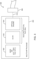
- FIG. 3 shows how multichip package 200 may include a main die 300 and an electro-optical tile 303.
- Main die 300 may be any suitable integrated circuit such as application specific integrated circuits (ASICs), programmable logic devices, application specific standard products (ASSPs), or other integrated circuits that include core processing circuitry or processing/logic circuitry configured to carry out a user application/function.
- Electro-optical tile 303 may include a transceiver component 302 and an optical engine (OE) component 304.
- Transceiver component 302 may be configured to handle electrical signals (e.g., digital and analog signals), whereas optical component 304 may be configured to handle primarily optical signals.
- transceiver 302 and optical engine 304 may be referred to collectively as an "electro-optical" tile.
- An external optical cable 306 may have a connector 308 configured to mate with optical engine component 304, as indicated by connection path 310. Mated in this way, external optical network signals can be fed directly to and from multichip package 200.
- interconnects between main die 300 and component 304 can be optimized for low power and high bandwidth density, which can help substantially reduce power consumption in a high-performance computing system while maintaining interconnect speeds of greater than 10 Gbps, 40 Gbps, 100 Gbps, 400 Gbps, etc.
- FIG. 4 is cross-sectional side view of an illustrative multiple package 200 with main die 300, a transceiver die 302, and optical engine dies 304 according to an embodiment.
- multichip package 200 includes a package substrate 400 with a top surface and a bottom surface, main die 300 mounted on the top surface of substrate 400, transceiver die 302 mounted on the top surface of substrate 400, and optical engine die 304 mounted on the top surface of substrate 400.
- An array of solder balls 402 (sometimes referred to collectively as a ball grid array or BGA) is formed at the bottom surface of package substrate 400.
- Main die 300, transceiver die 302, and optical engine die 304 are mounted on package substrate 200 using solder bumps 404 (e.g., controlled collapse chip connection (C4) bumps) and microbumps 406.
- solder bumps 404 e.g., controlled collapse chip connection (C4) bumps
- microbumps 406 microbumps 406.
- the pitch width of solder bumps 404 may be greater than the pitch width of microbumps 406, such that microbumps 406 have greater connectivity density than solder bumps 404.
- the diameter of microbumps 406 are also generally smaller than the diameter of C4 bumps 404 (e.g., bumps 406 may be at least two times smaller, at least four times smaller, etc.).
- Solder bumps 404 are also smaller than BGA solder balls 402.
- package 200 may include one or more embedded multi-die interconnect bridge (EMIB) components 408.
- EMIB is a small silicon die that is embedded in package substrate 400 and that offers dedicated ultra-high-density interconnection between dies within package 200.
- EMIBs generally include wires of minimal length, which help to significantly reduce loading and directly boost performance without consuming large amounts of power.
- EMIB solutions may be advantageous over other multichip packaging schemes that use a silicon interposer, which is prone to issues such as warpage and requires a comparatively large number of microbumps and through-silicon vias (TSVs) to be formed on and within the interposer, thereby reducing overall yield and increasing manufacturing complexity and cost.
- TSVs through-silicon vias
- the number of dies that can be integrated using an interposer is also limited to that supported by EMIB technology.
- main die 300 may be coupled to and convey signals to and from transceiver die 302 using a first EMIB 408 that is embedded in package substrate 400.
- main die 300 and transceiver die 302 interface with the first EMIB 408 using only microbumps 406, which supplies high density interconnectivity relative to C4 bumps 404.
- transceiver 302 may be coupled to and convey signals to and from optical engine die 304 using a second EMIB 408 that is embedded in package substrate 400.
- Transceiver die 302 and optical engine die 304 also interface with the second EMIB 408 using only microbumps 406, which supplies high density interconnectivity compared to C4 bumps 404.
- multichip package 200 may include more than one transceiver die 302 coupled to main die 300 via respective EMIB components.
- One or more additional optical engine dies are mounted on package substrate 400 or stacked on top of other dies (e.g., see additional optical engine die 304' stacked on top of transceiver die 302).
- multichip package 200 may include one main die 300 and four transceiver dies 302, two of which are coupled to one optical engine die 304 and another two of which are coupled to multiple optical engine dies 304.
- FIG. 5 is a diagram illustrating the interface between the transceiver die and the optical engine die within the multichip package.
- transceiver 302 may include a physical-layer interface portion (oftentimes abbreviated as "PHY"), which connects the physical medium through which data is conveyed to and from transceiver die 302 to an associated protocol processing circuit 500.
- PHY physical-layer interface portion
- the transceiver PHY may include a physical coding sublayer (PCS) and forward error correction (FEC) block 502, a serializer 504, a deserializer 506, a link management circuit 508, and/or other high-speed serial interface circuitry suitable for transmitting and receiving data.
- Block 502 may include, among others, decoders, encoders, data alignment circuitry, and registers such as first-in-first-out (FIFO) storage elements.
- Serializer 504 may be configured to transmit serialized data off of transceiver 302, whereas deserializer 506 may be configured to receive serialized data, deserialize the received data, and feed the deserialized data to block 502 for further processing.
- Management block 508 may be configured to control the operations of the transceiver PHY to ensure proper connection and data transfer.
- Protocol processing circuit 500 may serve as a data link layer component that is used to provide address and channel access control mechanisms to support unicast, multicast, or broadcast communications services. Protocol processing circuit 500 that is used to support an Ethernet link is sometimes referred to as a media access controller (MAC). In general, protocol processing circuit 208 may be used as the interface between the transceiver PHY and the main die to support any type of network communications protocol.
- MAC media access controller
- optical engine 304 may include channel driver 510, optical transmitter and laser component 512, optical receiver 514, and transimpedance amplifier (TIA) and limiting amplifier (LA) component 516.
- Channel driver 510 may be driven directly by the transceiver PHY (e.g., serializer 504 may directly drive channel driver 510 via EMIB path 520).
- Channel driver 510 may then generate corresponding output signals to component 512 so that optical signals can be output from optical engine 304 to an optical cable.
- Optical receiver 514 may receive signals from the external optical cable and may feed corresponding signals to component 516. Component may then feed the received signals directly to the transceiver PHY (e.g., deserializer 506 may receive signals directly from optical engine 304 via EMIB path 522) .
- Blocks 500 and 502 are configured to process signals in the digital domain.
- Blocks 504 and 506 in the transceiver PHY and blocks 510 and 516 in the optical engine are configured to process signals in the analog domain.
- Blocks 512 and 514 are configured to process signals in the optical domain.
- transceiver 302 and optical engine 304 are configured as an electro-optical tile that converts signals between the digital/electrical domain and the optical domain.
- FIG. 6 is a flow chart of illustrative steps for operating a multichip package of the type shown in FIGS. 2-5 .
- serializer 504 in the transceiver PHY may directly drive channel driver 510 in the optical engine.
- channel driver 510 may then output corresponding signals to optical transmitter 512.
- Optical transmitter 512 may then output signals via an external optical cable.
- transimpedance amplifier (TIA) and limiting amplifier (LA) block 516 may receive signals from optical receiver 514.
- deserializer 506 in the transceiver PHY may directly receive signals from block 516 in the optical engine. Deserializer 506 may then feed deserialized signals to the main die via blocks 502 and 500.
- multichip package 700 may include main die 300 and another die 702 that includes both the transceiver and optical engine circuits.
- the transceiver component and the optical engine component are collectively formed on a single auxiliary die 702 within package 700.
- an integrated circuit package such as single-chip package 800 may include one die 802 that includes the main processing and logic circuitry, the transceiver, and optical engine.
- the processing circuitry of the main integrated circuit e.g., circuitry of a PLD or ASIC
- the transceiver component and the optical engine component can all be collectively formed on a single die 802 within package 800.
- these components can be formed in any number of dies within an integrated circuit package. It is however pointed out that the scope of the present invention is defined by the appended claims.
Landscapes
- Physics & Mathematics (AREA)
- Electromagnetism (AREA)
- Engineering & Computer Science (AREA)
- Computer Networks & Wireless Communication (AREA)
- Signal Processing (AREA)
- General Physics & Mathematics (AREA)
- Optics & Photonics (AREA)
- Semiconductor Integrated Circuits (AREA)
- Optical Couplings Of Light Guides (AREA)
- Optical Communication System (AREA)
Claims (13)
- Integrierte-Schaltung-Gehäuse (200), das Folgendes umfasst:ein Verarbeitungsschaltungs-Die (300);ein Optik-Engine-Die (304), das mit dem Verarbeitungsschaltungs-Die (300) gekoppelt ist, wobei das Optik-Engine-Die (304) Optik-Engine-Schaltungen einschließlich eines optischen Senders und einer Laserkomponente (512) und eines optischen Empfängers (514) umfasst;ein Sendeempfänger-Die (302);ein Gehäusesubstrat (400) mit einer oberen Oberfläche, auf der das Verarbeitungsschaltungs-Die (300), das Sendeempfänger-Die (302) und das Optik-Engine-Die (304) unter Verwendung von Lötkontakthügeln (404) und/oder Mikrokontakthügeln (406) montiert sind;ein oder mehrere zusätzliche Optik-Engine-Dies, die auf dem Gehäusesubstrat montiert oder auf den Dies (300, 702) gestapelt sind; undleitfähige Signalleiterbahnen, die auf dem Gehäusesubstrat (400) gebildet sind, wobeidie Signalleiterbahnen das Verarbeitungsschaltungs-Die (300) direkt mit dem Sendeempfänger-Die (302) verbinden, und die Signalleiterbahnen das Sendeempfänger-Die (302) direkt mit dem Optik-Engine-Die (304) verbinden, wobei die Signalleiterbahnen mit dem Verarbeitungsschaltungs-Die (300), dem Sendeempfänger-Die (302) und dem Optik-Engine-Die (304) unter Verwendung der Lötkontakthügel (404) und/oder der Mikrokontakthügel (406) verbunden sind.
- Integrierte-Schaltung-Gehäuse (200) nach Anspruch 1, wobei das Verarbeitungsschaltungs-Die (300) ein FPGA ist.
- Integrierte-Schaltung-Gehäuse nach Anspruch 1 oder 2, wobei die Optik-Engine (304) mit einem externen optischen Kabel (306) gekoppelt ist, das zur direkten Kopplung mit dem Integrierte-Schaltung-Gehäuse ausgelegt ist.
- Integrierte-Schaltung-Gehäuse nach Anspruch 1, wobei das Sendeempfänger-Die (302) eine Sendeempfänger-Die-Physical-Layer-Schaltung umfasst, wobei das Optik-Engine-Die (304) einen Kanaltreiber umfasst und wobei die Sendeempfänger-Die-Physical-Layer-Schaltung den Kanaltreiber direkt ansteuert.
- Integrierte-Schaltung-Gehäuse nach Anspruch 4, wobei die Sendeempfänger-Die-Physical-Layer-Schaltung Folgendes umfasst:einen Serializer, der den Kanaltreiber der Optik-Engine (304) direkt ansteuert; undeinen Deserializer, der Signale direkt von einem Transimpedanzverstärker und Begrenzungsverstärkerblock in der Optik-Engine (304) empfängt.
- Integrierte-Schaltung-Gehäuse nach einem der Ansprüche 1-5, ferner umfassend eine zusätzliche Optik-Engine (304'), die auf dem Sendeempfänger-Die (302) montiert ist.
- Integrierte-Schaltung-Gehäuse nach Anspruch 1, wobei der Sendeempfänger Folgendes umfasst: eine Medienzugriffssteuerung; einen Physische-Codierungssubschicht- und Vorwärtsfehlerkorrekturblock, ausgelegt zum Empfangen von Signalen von der Medienzugriffssteuerung; einen Serializer, ausgelegt zum Empfangen von Signalen von dem Physische-Codierungssubschicht- und Vorwärtsfehlerkorrekturblock; und einen Deserializer, ausgelegt zum Ausgeben von Signalen an den Physische-Codierungssubschicht- und Vorwärtsfehlerkorrekturblock.
- Integrierte-Schaltung-Gehäuse nach Anspruch 1, wobei die Optik-Engine Folgendes umfasst: einen Kanaltreiber, der dazu ausgelegt ist, direkt durch einen Serializer angesteuert zu werden; wobei der optische Sender dazu ausgelegt ist, Signale von dem Kanaltreiber zu empfangen; und einen Verstärkerblock, ausgelegt zum Empfangen von Signalen von dem optischen Empfänger, wobei der Verstärkerblock dazu ausgelegt ist, den Deserializer direkt anzusteuern.
- System, umfassend ein Integrierte-Schaltung-Gehäuse (200) nach einem der vorhergehenden Ansprüche und ein optisches Kabel, wobei die Optik-Engine (304) des Integrierte-Schaltung-Gehäuses (200) mit dem optischen Kabel (306) gekoppelt ist, sodass externe optische Netzwerksignale zu und von dem Integrierte-Schaltung-Gehäuse (200) geleitet werden können.
- Verfahren zum Betreiben eines Integrierte-Schaltung-Gehäuse nach einem der Ansprüche 1-9, wobei das Verfahren Folgendes umfasst:mit dem Verarbeitungsschaltungs-Die (300), Senden von Signalen an das Optik-Engine-Die (304) über Signalleiterbahnen, die das Verarbeitungsschaltungs-Die (300) direkt mit dem Sendeempfänger-Die (302) verbinden, und Signalleiterbahnen, die das Sendeempfänger-Die (302) direkt mit dem Optik-Engine-Die (304) verbinden; undmit dem Optik-Engine-Die (304), Empfangen der Signale von dem Verarbeitungsschaltungs-Die (300) und Ausgeben entsprechender optischer Signale an ein externes optisches Kabel (306), das direkt mit dem Integrierte-Schaltung-Gehäuse verbunden ist.
- Verfahren nach Anspruch 10, das ferner Folgendes umfasst:
mit einer Physical-Layer-Komponente in dem Sendeempfänger-Die (302), direktes Ansteuern des Optik-Engine-Die (304). - Verfahren nach Anspruch 11, wobei das direkte Ansteuern des Optik-Engine-Die (304) mit der Physical-Layer-Komponente in dem Sendeempfänger-Die (302) Folgendes umfasst:
mit einem Serializer in der Physical-Layer-Komponente des Sendeempfänger-Die (302), direktes Ansteuern eines Kanaltreibers in dem Optik-Engine-Die (304). - Verfahren nach Anspruch 12, wobei das direkte Ansteuern des Optik-Engine-Die (304) mit der Physical-Layer-Komponente in dem Sendeempfänger-Die (302) ferner Folgendes umfasst:
mit einem Deserializer in der Physical-Layer-Komponente des Sendeempfänger-Die (302), direktes Empfangen von Signalen von einem Transimpedanz- und Begrenzungsverstärkerblock in dem Optik-Engine-Die (304) .
Applications Claiming Priority (1)
| Application Number | Priority Date | Filing Date | Title |
|---|---|---|---|
| US15/835,177 US11327259B2 (en) | 2017-12-07 | 2017-12-07 | Integrated circuit package with electro-optical interconnect circuitry |
Publications (2)
| Publication Number | Publication Date |
|---|---|
| EP3496300A1 EP3496300A1 (de) | 2019-06-12 |
| EP3496300B1 true EP3496300B1 (de) | 2025-03-26 |
Family
ID=64331623
Family Applications (1)
| Application Number | Title | Priority Date | Filing Date |
|---|---|---|---|
| EP18204765.4A Active EP3496300B1 (de) | 2017-12-07 | 2018-11-06 | Integriertes schaltungspaket mit elektrooptischer verbindungsschaltung |
Country Status (3)
| Country | Link |
|---|---|
| US (3) | US11327259B2 (de) |
| EP (1) | EP3496300B1 (de) |
| CN (1) | CN109904141A (de) |
Families Citing this family (18)
| Publication number | Priority date | Publication date | Assignee | Title |
|---|---|---|---|---|
| US9236366B2 (en) * | 2012-12-20 | 2016-01-12 | Intel Corporation | High density organic bridge device and method |
| US11327259B2 (en) * | 2017-12-07 | 2022-05-10 | Intel Corporation | Integrated circuit package with electro-optical interconnect circuitry |
| US11493689B2 (en) * | 2019-09-19 | 2022-11-08 | Taiwan Semiconductor Manufacturing Co., Ltd. | Photonic semiconductor device and method of manufacture |
| US12500182B2 (en) * | 2020-01-31 | 2025-12-16 | Sony Semiconductor Solutions Corporation | Substrate and semiconductor package |
| EP4115223B1 (de) | 2020-04-13 | 2025-10-15 | Avicenatech, Corp. | Optisch verbesserte multichip-verpackung |
| US12266608B2 (en) * | 2020-06-25 | 2025-04-01 | Intel Corporation | Integrated photonics and processor package with redistribution layer and EMIB connector |
| US20220094434A1 (en) * | 2020-09-24 | 2022-03-24 | Intel Corporation | Characterizing data transmitted over an optical link based on one or more wavelengths used in transmission |
| US20220092016A1 (en) * | 2020-09-24 | 2022-03-24 | Intel Corporation | Off-package high density, high bandwidth memory access using optical links |
| CN115185045B (zh) * | 2021-04-02 | 2023-09-15 | 中国科学院微电子研究所 | 一种光纤拉远处理器模组结构 |
| US11894354B2 (en) * | 2021-05-13 | 2024-02-06 | Advanced Semiconductor Engineering, Inc. | Optoelectronic device package and method of manufacturing the same |
| CN115515027A (zh) * | 2021-06-03 | 2022-12-23 | 华为技术有限公司 | 光电混合封装结构和电子设备 |
| US20230200119A1 (en) * | 2021-12-20 | 2023-06-22 | Intel Corporation | Organic thin-films for data transmission |
| CN114371537B (zh) * | 2022-02-17 | 2024-06-25 | Nano科技(北京)有限公司 | 一种分体式集成封装光模块 |
| US12442997B2 (en) * | 2022-03-18 | 2025-10-14 | Celestial AI, Inc. | Optically bridged multicomponent package with extended temperature range |
| US11835777B2 (en) | 2022-03-18 | 2023-12-05 | Celestial Ai Inc. | Optical multi-die interconnect bridge (OMIB) |
| US20230396351A1 (en) * | 2022-06-03 | 2023-12-07 | Aloe Semiconductor, Inc. | Optical multi-wavelength dual-polarization transceivers |
| US20240103238A1 (en) * | 2022-09-22 | 2024-03-28 | Apple Inc. | 3D System and Wafer Reconstitution with Mid-layer Interposer |
| CN117316894B (zh) * | 2023-09-28 | 2024-03-22 | 浙江睿兆芯半导体科技有限公司 | 一种融合多种芯片封装的单一封装体 |
Citations (2)
| Publication number | Priority date | Publication date | Assignee | Title |
|---|---|---|---|---|
| US20160142155A1 (en) * | 2014-11-17 | 2016-05-19 | SK Hynix Inc. | Semiconductor packages with optical interconnection structures, memory cards including the same, and electronic systems including the same |
| US20170194309A1 (en) * | 2016-01-04 | 2017-07-06 | Infinera Corporation | Photonic integrated circuit package |
Family Cites Families (37)
| Publication number | Priority date | Publication date | Assignee | Title |
|---|---|---|---|---|
| US6909419B2 (en) * | 1997-10-31 | 2005-06-21 | Kopin Corporation | Portable microdisplay system |
| US7079775B2 (en) * | 2001-02-05 | 2006-07-18 | Finisar Corporation | Integrated memory mapped controller circuit for fiber optics transceiver |
| US6975642B2 (en) | 2001-09-17 | 2005-12-13 | Finisar Corporation | Optoelectronic device capable of participating in in-band traffic |
| US7286622B2 (en) | 2002-08-07 | 2007-10-23 | Broadcom Corporation | System and method for performing on-chip synchronization of system signals utilizing off-chip harmonic signal |
| US6789959B1 (en) * | 2003-02-27 | 2004-09-14 | Xilinx, Inc. | Fiber optic integrated circuit package using micromirrors |
| US6945712B1 (en) * | 2003-02-27 | 2005-09-20 | Xilinx, Inc. | Fiber optic field programmable gate array integrated circuit packaging |
| US7132746B2 (en) * | 2003-08-18 | 2006-11-07 | Delphi Technologies, Inc. | Electronic assembly with solder-bonded heat sink |
| US20050105574A1 (en) * | 2003-11-14 | 2005-05-19 | Wu Xin M. | Laser driver for optical communication network |
| US7183641B2 (en) * | 2005-03-30 | 2007-02-27 | Intel Corporation | Integrated heat spreader with intermetallic layer and method for making |
| US8666257B2 (en) * | 2007-05-24 | 2014-03-04 | Finisar Corporation | Optoelectronic devices with intelligent transmitter modules |
| US8030757B2 (en) * | 2007-06-29 | 2011-10-04 | Intel Corporation | Forming a semiconductor package including a thermal interface material |
| US20090116845A1 (en) | 2007-11-02 | 2009-05-07 | Wen Li | Tetintelligent optical transceiver capable of optical-layer management |
| US8227904B2 (en) * | 2009-06-24 | 2012-07-24 | Intel Corporation | Multi-chip package and method of providing die-to-die interconnects in same |
| US9002155B2 (en) * | 2011-03-28 | 2015-04-07 | Altera Corporation | Integrated optical-electronic interface in programmable integrated circuit device |
| KR101356472B1 (ko) * | 2011-07-01 | 2014-02-03 | 샘텍, 인코포레이티드 | Ic 패키지용 인터페이스 및 트랜스시버 |
| US20130230272A1 (en) * | 2012-03-01 | 2013-09-05 | Oracle International Corporation | Chip assembly configuration with densely packed optical interconnects |
| EP2873175B1 (de) | 2012-07-15 | 2023-05-17 | OE Solutions America Inc. | Steuersysteme für optische vorrichtungen und baugruppen |
| US8546955B1 (en) * | 2012-08-16 | 2013-10-01 | Xilinx, Inc. | Multi-die stack package |
| US8946900B2 (en) * | 2012-10-31 | 2015-02-03 | Intel Corporation | X-line routing for dense multi-chip-package interconnects |
| US8901748B2 (en) * | 2013-03-14 | 2014-12-02 | Intel Corporation | Direct external interconnect for embedded interconnect bridge package |
| US9250403B2 (en) * | 2013-04-26 | 2016-02-02 | Oracle International Corporation | Hybrid-integrated photonic chip package with an interposer |
| US8916981B2 (en) * | 2013-05-10 | 2014-12-23 | Intel Corporation | Epoxy-amine underfill materials for semiconductor packages |
| US9041205B2 (en) * | 2013-06-28 | 2015-05-26 | Intel Corporation | Reliable microstrip routing for electronics components |
| US20150220472A1 (en) * | 2014-02-05 | 2015-08-06 | Qualcomm Incorporated | Increasing throughput on multi-wire and multi-lane interfaces |
| JP6195995B2 (ja) * | 2014-02-26 | 2017-09-20 | インテル コーポレイション | ブリッジ貫通導電ビア信号接続を有する埋込マルチデバイスブリッジ |
| US9671572B2 (en) * | 2014-09-22 | 2017-06-06 | Oracle International Corporation | Integrated chip package with optical interface |
| US9692402B2 (en) * | 2014-12-25 | 2017-06-27 | Intel Corporation | Method, apparatus, system for centering in a high performance interconnect |
| US9971089B2 (en) * | 2015-12-09 | 2018-05-15 | Intel Corporation | Chip-to-chip interconnect with embedded electro-optical bridge structures |
| US9832006B1 (en) * | 2016-05-24 | 2017-11-28 | Intel Corporation | Method, apparatus and system for deskewing parallel interface links |
| US10218360B2 (en) * | 2016-08-02 | 2019-02-26 | Altera Corporation | Dynamic clock-data phase alignment in a source synchronous interface circuit |
| US10672663B2 (en) * | 2016-10-07 | 2020-06-02 | Xcelsis Corporation | 3D chip sharing power circuit |
| US10622311B2 (en) * | 2017-08-10 | 2020-04-14 | International Business Machines Corporation | High-density interconnecting adhesive tape |
| US10313104B2 (en) * | 2017-09-18 | 2019-06-04 | Avago Technologies International Sales Pte. Limited | System and method for controlling the impact of periodic jitter caused by non-ideal phase interpolators |
| US11327259B2 (en) * | 2017-12-07 | 2022-05-10 | Intel Corporation | Integrated circuit package with electro-optical interconnect circuitry |
| GB2572641B (en) * | 2018-04-06 | 2021-06-02 | Rockley Photonics Ltd | Optoelectronic device and array thereof |
| US10530614B2 (en) * | 2018-12-21 | 2020-01-07 | Intel Corporation | Short link efficient interconnect circuitry |
| US11418312B2 (en) * | 2019-04-19 | 2022-08-16 | Infinera Corporation | Synchronization for subcarrier communication |
-
2017
- 2017-12-07 US US15/835,177 patent/US11327259B2/en active Active
-
2018
- 2018-11-06 EP EP18204765.4A patent/EP3496300B1/de active Active
- 2018-11-07 CN CN201811318514.6A patent/CN109904141A/zh active Pending
-
2022
- 2022-04-18 US US17/723,174 patent/US12055777B2/en active Active
-
2024
- 2024-08-05 US US18/795,148 patent/US20240418951A1/en active Pending
Patent Citations (2)
| Publication number | Priority date | Publication date | Assignee | Title |
|---|---|---|---|---|
| US20160142155A1 (en) * | 2014-11-17 | 2016-05-19 | SK Hynix Inc. | Semiconductor packages with optical interconnection structures, memory cards including the same, and electronic systems including the same |
| US20170194309A1 (en) * | 2016-01-04 | 2017-07-06 | Infinera Corporation | Photonic integrated circuit package |
Non-Patent Citations (2)
| Title |
|---|
| LI CHENHUI ET AL: "Chip Scale 12-Channel 10 Gb/s Optical Transmitter and Receiver Subassemblies Based on Wet Etched Silicon Interposer", JOURNAL OF LIGHTWAVE TECHNOLOGY, IEEE, USA, vol. 35, no. 15, 1 August 2017 (2017-08-01), pages 3229 - 3236, XP011655577, ISSN: 0733-8724, [retrieved on 20170706], DOI: 10.1109/JLT.2017.2681043 * |
| MAHAJAN RAVI ET AL: "Embedded Multi-die Interconnect Bridge (EMIB) -- A High Density, High Bandwidth Packaging Interconnect", 2016 IEEE 66TH ELECTRONIC COMPONENTS AND TECHNOLOGY CONFERENCE (ECTC), IEEE, 31 May 2016 (2016-05-31), pages 557 - 565, XP032947599, DOI: 10.1109/ECTC.2016.201 * |
Also Published As
| Publication number | Publication date |
|---|---|
| US11327259B2 (en) | 2022-05-10 |
| US20240418951A1 (en) | 2024-12-19 |
| US20190041594A1 (en) | 2019-02-07 |
| EP3496300A1 (de) | 2019-06-12 |
| CN109904141A (zh) | 2019-06-18 |
| US20220244477A1 (en) | 2022-08-04 |
| US12055777B2 (en) | 2024-08-06 |
Similar Documents
| Publication | Publication Date | Title |
|---|---|---|
| US12055777B2 (en) | Integrated circuit package with electro-optical interconnect circuitry | |
| US11842986B1 (en) | Multi-chip module (MCM) with interface adapter circuitry | |
| CN121241437A (zh) | 小芯片到小芯片协议切换 | |
| US11841815B1 (en) | Chiplet gearbox for low-cost multi-chip module applications | |
| US11581282B2 (en) | Serializer-deserializer die for high speed signal interconnect | |
| US11669479B2 (en) | Multichip package with protocol-configurable data paths | |
| US8238359B2 (en) | Communication module and communication apparatus | |
| US7044658B1 (en) | High speed serial I/O technology using an optical link | |
| US20250038163A1 (en) | Optical multichip package with multiple system-on-chip dies | |
| US20220158736A1 (en) | Optical Module and Method of Fabrication | |
| US12438618B2 (en) | Pseudo-monolithic data communication system | |
| EP2820461A2 (de) | Konfiguration einer chip-anordnung mit optischen verbindungen mit hoher packungsdichte | |
| US20210326292A1 (en) | Multi-package system using configurable input/output interface circuits for single-ended intra-package communication and differential inter-package communication | |
| KR20250121434A (ko) | 광학 통신 기판을 사용하는 칩렛 통신 | |
| US12314208B2 (en) | Systems, apparatuses, methods, and non-transitory computer-readable storage devices for de-serializing and serializing data transmission | |
| US20030185499A1 (en) | High speed optical interconnects | |
| US12579093B1 (en) | Chiplet gearbox for low-cost multi-chip module applications | |
| US20260142724A1 (en) | Integrated, High-Speed Optical Transceiver | |
| US20260140338A1 (en) | Integrated, High-Speed Optical Transceiver | |
| KR20250018188A (ko) | 칩간 연결을 위한 실리콘 포토닉스 광 수신기 | |
| WO2026059746A1 (en) | Integrated, high-speed optical transceiver |
Legal Events
| Date | Code | Title | Description |
|---|---|---|---|
| PUAI | Public reference made under article 153(3) epc to a published international application that has entered the european phase |
Free format text: ORIGINAL CODE: 0009012 |
|
| STAA | Information on the status of an ep patent application or granted ep patent |
Free format text: STATUS: THE APPLICATION HAS BEEN PUBLISHED |
|
| AK | Designated contracting states |
Kind code of ref document: A1 Designated state(s): AL AT BE BG CH CY CZ DE DK EE ES FI FR GB GR HR HU IE IS IT LI LT LU LV MC MK MT NL NO PL PT RO RS SE SI SK SM TR |
|
| AX | Request for extension of the european patent |
Extension state: BA ME |
|
| STAA | Information on the status of an ep patent application or granted ep patent |
Free format text: STATUS: REQUEST FOR EXAMINATION WAS MADE |
|
| 17P | Request for examination filed |
Effective date: 20191212 |
|
| RBV | Designated contracting states (corrected) |
Designated state(s): AL AT BE BG CH CY CZ DE DK EE ES FI FR GB GR HR HU IE IS IT LI LT LU LV MC MK MT NL NO PL PT RO RS SE SI SK SM TR |
|
| STAA | Information on the status of an ep patent application or granted ep patent |
Free format text: STATUS: EXAMINATION IS IN PROGRESS |
|
| 17Q | First examination report despatched |
Effective date: 20210125 |
|
| GRAP | Despatch of communication of intention to grant a patent |
Free format text: ORIGINAL CODE: EPIDOSNIGR1 |
|
| STAA | Information on the status of an ep patent application or granted ep patent |
Free format text: STATUS: GRANT OF PATENT IS INTENDED |
|
| GRAS | Grant fee paid |
Free format text: ORIGINAL CODE: EPIDOSNIGR3 |
|
| INTG | Intention to grant announced |
Effective date: 20250117 |
|
| GRAA | (expected) grant |
Free format text: ORIGINAL CODE: 0009210 |
|
| STAA | Information on the status of an ep patent application or granted ep patent |
Free format text: STATUS: THE PATENT HAS BEEN GRANTED |
|
| AK | Designated contracting states |
Kind code of ref document: B1 Designated state(s): AL AT BE BG CH CY CZ DE DK EE ES FI FR GB GR HR HU IE IS IT LI LT LU LV MC MK MT NL NO PL PT RO RS SE SI SK SM TR |
|
| REG | Reference to a national code |
Ref country code: GB Ref legal event code: FG4D |
|
| REG | Reference to a national code |
Ref country code: CH Ref legal event code: EP |
|
| REG | Reference to a national code |
Ref country code: DE Ref legal event code: R096 Ref document number: 602018080424 Country of ref document: DE |
|
| REG | Reference to a national code |
Ref country code: IE Ref legal event code: FG4D |
|
| P01 | Opt-out of the competence of the unified patent court (upc) registered |
Free format text: CASE NUMBER: APP_15019/2025 Effective date: 20250327 |
|
| REG | Reference to a national code |
Ref country code: NL Ref legal event code: FP |
|
| PG25 | Lapsed in a contracting state [announced via postgrant information from national office to epo] |
Ref country code: RS Free format text: LAPSE BECAUSE OF FAILURE TO SUBMIT A TRANSLATION OF THE DESCRIPTION OR TO PAY THE FEE WITHIN THE PRESCRIBED TIME-LIMIT Effective date: 20250626 |
|
| PG25 | Lapsed in a contracting state [announced via postgrant information from national office to epo] |
Ref country code: FI Free format text: LAPSE BECAUSE OF FAILURE TO SUBMIT A TRANSLATION OF THE DESCRIPTION OR TO PAY THE FEE WITHIN THE PRESCRIBED TIME-LIMIT Effective date: 20250326 |
|
| REG | Reference to a national code |
Ref country code: LT Ref legal event code: MG9D |
|
| PG25 | Lapsed in a contracting state [announced via postgrant information from national office to epo] |
Ref country code: NO Free format text: LAPSE BECAUSE OF FAILURE TO SUBMIT A TRANSLATION OF THE DESCRIPTION OR TO PAY THE FEE WITHIN THE PRESCRIBED TIME-LIMIT Effective date: 20250626 |
|
| PG25 | Lapsed in a contracting state [announced via postgrant information from national office to epo] |
Ref country code: HR Free format text: LAPSE BECAUSE OF FAILURE TO SUBMIT A TRANSLATION OF THE DESCRIPTION OR TO PAY THE FEE WITHIN THE PRESCRIBED TIME-LIMIT Effective date: 20250326 |
|
| PG25 | Lapsed in a contracting state [announced via postgrant information from national office to epo] |
Ref country code: LV Free format text: LAPSE BECAUSE OF FAILURE TO SUBMIT A TRANSLATION OF THE DESCRIPTION OR TO PAY THE FEE WITHIN THE PRESCRIBED TIME-LIMIT Effective date: 20250326 |
|
| PG25 | Lapsed in a contracting state [announced via postgrant information from national office to epo] |
Ref country code: GR Free format text: LAPSE BECAUSE OF FAILURE TO SUBMIT A TRANSLATION OF THE DESCRIPTION OR TO PAY THE FEE WITHIN THE PRESCRIBED TIME-LIMIT Effective date: 20250627 Ref country code: BG Free format text: LAPSE BECAUSE OF FAILURE TO SUBMIT A TRANSLATION OF THE DESCRIPTION OR TO PAY THE FEE WITHIN THE PRESCRIBED TIME-LIMIT Effective date: 20250326 |
|
| PG25 | Lapsed in a contracting state [announced via postgrant information from national office to epo] |
Ref country code: SE Free format text: LAPSE BECAUSE OF FAILURE TO SUBMIT A TRANSLATION OF THE DESCRIPTION OR TO PAY THE FEE WITHIN THE PRESCRIBED TIME-LIMIT Effective date: 20250326 |
|
| REG | Reference to a national code |
Ref country code: AT Ref legal event code: MK05 Ref document number: 1780008 Country of ref document: AT Kind code of ref document: T Effective date: 20250326 |
|
| PG25 | Lapsed in a contracting state [announced via postgrant information from national office to epo] |
Ref country code: SM Free format text: LAPSE BECAUSE OF FAILURE TO SUBMIT A TRANSLATION OF THE DESCRIPTION OR TO PAY THE FEE WITHIN THE PRESCRIBED TIME-LIMIT Effective date: 20250326 |
|
| REG | Reference to a national code |
Ref country code: CH Ref legal event code: W10 Free format text: ST27 STATUS EVENT CODE: U-0-0-W10-W00 (AS PROVIDED BY THE NATIONAL OFFICE) Effective date: 20251008 |
|
| PG25 | Lapsed in a contracting state [announced via postgrant information from national office to epo] |
Ref country code: PT Free format text: LAPSE BECAUSE OF FAILURE TO SUBMIT A TRANSLATION OF THE DESCRIPTION OR TO PAY THE FEE WITHIN THE PRESCRIBED TIME-LIMIT Effective date: 20250728 Ref country code: ES Free format text: LAPSE BECAUSE OF FAILURE TO SUBMIT A TRANSLATION OF THE DESCRIPTION OR TO PAY THE FEE WITHIN THE PRESCRIBED TIME-LIMIT Effective date: 20250326 |
|
| PG25 | Lapsed in a contracting state [announced via postgrant information from national office to epo] |
Ref country code: IT Free format text: LAPSE BECAUSE OF FAILURE TO SUBMIT A TRANSLATION OF THE DESCRIPTION OR TO PAY THE FEE WITHIN THE PRESCRIBED TIME-LIMIT Effective date: 20250326 Ref country code: PL Free format text: LAPSE BECAUSE OF FAILURE TO SUBMIT A TRANSLATION OF THE DESCRIPTION OR TO PAY THE FEE WITHIN THE PRESCRIBED TIME-LIMIT Effective date: 20250326 |
|
| PGFP | Annual fee paid to national office [announced via postgrant information from national office to epo] |
Ref country code: NL Payment date: 20250924 Year of fee payment: 8 |
|
| REG | Reference to a national code |
Ref country code: DE Ref legal event code: R081 Ref document number: 602018080424 Country of ref document: DE Owner name: ALTERA CORPORATION, SAN JOSE, US Free format text: FORMER OWNER: INTEL CORPORATION, SANTA CLARA, CA, US |
|
| PG25 | Lapsed in a contracting state [announced via postgrant information from national office to epo] |
Ref country code: AT Free format text: LAPSE BECAUSE OF FAILURE TO SUBMIT A TRANSLATION OF THE DESCRIPTION OR TO PAY THE FEE WITHIN THE PRESCRIBED TIME-LIMIT Effective date: 20250326 |
|
| PG25 | Lapsed in a contracting state [announced via postgrant information from national office to epo] |
Ref country code: EE Free format text: LAPSE BECAUSE OF FAILURE TO SUBMIT A TRANSLATION OF THE DESCRIPTION OR TO PAY THE FEE WITHIN THE PRESCRIBED TIME-LIMIT Effective date: 20250326 |
|
| REG | Reference to a national code |
Ref country code: NL Ref legal event code: PD Owner name: ALTERA CORPORATION; US Free format text: DETAILS ASSIGNMENT: CHANGE OF OWNER(S), ASSIGNMENT; FORMER OWNER NAME: INTEL CORPORATION Effective date: 20251013 |
|
| PG25 | Lapsed in a contracting state [announced via postgrant information from national office to epo] |
Ref country code: RO Free format text: LAPSE BECAUSE OF FAILURE TO SUBMIT A TRANSLATION OF THE DESCRIPTION OR TO PAY THE FEE WITHIN THE PRESCRIBED TIME-LIMIT Effective date: 20250326 |
|
| PG25 | Lapsed in a contracting state [announced via postgrant information from national office to epo] |
Ref country code: SK Free format text: LAPSE BECAUSE OF FAILURE TO SUBMIT A TRANSLATION OF THE DESCRIPTION OR TO PAY THE FEE WITHIN THE PRESCRIBED TIME-LIMIT Effective date: 20250326 |
|
| PG25 | Lapsed in a contracting state [announced via postgrant information from national office to epo] |
Ref country code: IS Free format text: LAPSE BECAUSE OF FAILURE TO SUBMIT A TRANSLATION OF THE DESCRIPTION OR TO PAY THE FEE WITHIN THE PRESCRIBED TIME-LIMIT Effective date: 20250726 |
|
| RAP2 | Party data changed (patent owner data changed or rights of a patent transferred) |
Owner name: ALTERA CORPORATION |
|
| REG | Reference to a national code |
Ref country code: DE Ref legal event code: R097 Ref document number: 602018080424 Country of ref document: DE |
|
| PGFP | Annual fee paid to national office [announced via postgrant information from national office to epo] |
Ref country code: DE Payment date: 20250923 Year of fee payment: 8 |
|
| PG25 | Lapsed in a contracting state [announced via postgrant information from national office to epo] |
Ref country code: DK Free format text: LAPSE BECAUSE OF FAILURE TO SUBMIT A TRANSLATION OF THE DESCRIPTION OR TO PAY THE FEE WITHIN THE PRESCRIBED TIME-LIMIT Effective date: 20250326 |
|
| PG25 | Lapsed in a contracting state [announced via postgrant information from national office to epo] |
Ref country code: CZ Free format text: LAPSE BECAUSE OF FAILURE TO SUBMIT A TRANSLATION OF THE DESCRIPTION OR TO PAY THE FEE WITHIN THE PRESCRIBED TIME-LIMIT Effective date: 20250326 |
|
| PLBE | No opposition filed within time limit |
Free format text: ORIGINAL CODE: 0009261 |
|
| STAA | Information on the status of an ep patent application or granted ep patent |
Free format text: STATUS: NO OPPOSITION FILED WITHIN TIME LIMIT |
|
| REG | Reference to a national code |
Ref country code: CH Ref legal event code: L10 Free format text: ST27 STATUS EVENT CODE: U-0-0-L10-L00 (AS PROVIDED BY THE NATIONAL OFFICE) Effective date: 20260211 |
|
| 26N | No opposition filed |
Effective date: 20260105 |