EP3494433B1 - Light deflector, optical scanning device, image projection device, and mobile object - Google Patents
Light deflector, optical scanning device, image projection device, and mobile object Download PDFInfo
- Publication number
- EP3494433B1 EP3494433B1 EP17826586.4A EP17826586A EP3494433B1 EP 3494433 B1 EP3494433 B1 EP 3494433B1 EP 17826586 A EP17826586 A EP 17826586A EP 3494433 B1 EP3494433 B1 EP 3494433B1
- Authority
- EP
- European Patent Office
- Prior art keywords
- driving
- unit
- light deflector
- light
- piezoelectric
- Prior art date
- Legal status (The legal status is an assumption and is not a legal conclusion. Google has not performed a legal analysis and makes no representation as to the accuracy of the status listed.)
- Active
Links
- 230000003287 optical effect Effects 0.000 title claims description 100
- 239000000463 material Substances 0.000 claims description 8
- XUIMIQQOPSSXEZ-UHFFFAOYSA-N Silicon Chemical compound [Si] XUIMIQQOPSSXEZ-UHFFFAOYSA-N 0.000 description 31
- 229910052710 silicon Inorganic materials 0.000 description 31
- 239000010703 silicon Substances 0.000 description 31
- 238000010586 diagram Methods 0.000 description 19
- 230000006870 function Effects 0.000 description 14
- 238000012545 processing Methods 0.000 description 14
- 230000010355 oscillation Effects 0.000 description 11
- 239000000758 substrate Substances 0.000 description 11
- VYPSYNLAJGMNEJ-UHFFFAOYSA-N Silicium dioxide Chemical compound O=[Si]=O VYPSYNLAJGMNEJ-UHFFFAOYSA-N 0.000 description 9
- 230000000717 retained effect Effects 0.000 description 9
- 229910052814 silicon oxide Inorganic materials 0.000 description 9
- 230000007423 decrease Effects 0.000 description 7
- 239000000470 constituent Substances 0.000 description 6
- 230000008878 coupling Effects 0.000 description 6
- 238000010168 coupling process Methods 0.000 description 6
- 238000005859 coupling reaction Methods 0.000 description 6
- BASFCYQUMIYNBI-UHFFFAOYSA-N platinum Chemical compound [Pt] BASFCYQUMIYNBI-UHFFFAOYSA-N 0.000 description 6
- 239000010931 gold Substances 0.000 description 5
- 238000006073 displacement reaction Methods 0.000 description 4
- 229910052451 lead zirconate titanate Inorganic materials 0.000 description 4
- 230000004048 modification Effects 0.000 description 4
- 238000012986 modification Methods 0.000 description 4
- 230000000630 rising effect Effects 0.000 description 4
- 230000015572 biosynthetic process Effects 0.000 description 3
- 230000000694 effects Effects 0.000 description 3
- 238000005530 etching Methods 0.000 description 3
- PCHJSUWPFVWCPO-UHFFFAOYSA-N gold Chemical compound [Au] PCHJSUWPFVWCPO-UHFFFAOYSA-N 0.000 description 3
- 229910052737 gold Inorganic materials 0.000 description 3
- IJGRMHOSHXDMSA-UHFFFAOYSA-N Atomic nitrogen Chemical compound N#N IJGRMHOSHXDMSA-UHFFFAOYSA-N 0.000 description 2
- 229910052782 aluminium Inorganic materials 0.000 description 2
- XAGFODPZIPBFFR-UHFFFAOYSA-N aluminium Chemical compound [Al] XAGFODPZIPBFFR-UHFFFAOYSA-N 0.000 description 2
- 238000001514 detection method Methods 0.000 description 2
- HFGPZNIAWCZYJU-UHFFFAOYSA-N lead zirconate titanate Chemical compound [O-2].[O-2].[O-2].[O-2].[O-2].[Ti+4].[Zr+4].[Pb+2] HFGPZNIAWCZYJU-UHFFFAOYSA-N 0.000 description 2
- 238000000034 method Methods 0.000 description 2
- 238000004806 packaging method and process Methods 0.000 description 2
- 229910052697 platinum Inorganic materials 0.000 description 2
- BQCADISMDOOEFD-UHFFFAOYSA-N Silver Chemical compound [Ag] BQCADISMDOOEFD-UHFFFAOYSA-N 0.000 description 1
- 230000004075 alteration Effects 0.000 description 1
- 230000003667 anti-reflective effect Effects 0.000 description 1
- 210000000988 bone and bone Anatomy 0.000 description 1
- 210000005252 bulbus oculi Anatomy 0.000 description 1
- 230000015556 catabolic process Effects 0.000 description 1
- 239000003086 colorant Substances 0.000 description 1
- 238000004891 communication Methods 0.000 description 1
- 230000008602 contraction Effects 0.000 description 1
- 230000003247 decreasing effect Effects 0.000 description 1
- 238000006731 degradation reaction Methods 0.000 description 1
- 230000000593 degrading effect Effects 0.000 description 1
- 230000007613 environmental effect Effects 0.000 description 1
- 239000010408 film Substances 0.000 description 1
- 230000012447 hatching Effects 0.000 description 1
- 210000003128 head Anatomy 0.000 description 1
- 238000010438 heat treatment Methods 0.000 description 1
- 238000003384 imaging method Methods 0.000 description 1
- 239000011261 inert gas Substances 0.000 description 1
- 238000009434 installation Methods 0.000 description 1
- 239000012212 insulator Substances 0.000 description 1
- 238000002372 labelling Methods 0.000 description 1
- 238000005259 measurement Methods 0.000 description 1
- 239000002184 metal Substances 0.000 description 1
- 229910052751 metal Inorganic materials 0.000 description 1
- 238000005459 micromachining Methods 0.000 description 1
- 229910021421 monocrystalline silicon Inorganic materials 0.000 description 1
- 229910052757 nitrogen Inorganic materials 0.000 description 1
- 230000003647 oxidation Effects 0.000 description 1
- 238000007254 oxidation reaction Methods 0.000 description 1
- 230000010287 polarization Effects 0.000 description 1
- 230000009467 reduction Effects 0.000 description 1
- 230000003014 reinforcing effect Effects 0.000 description 1
- 229910052709 silver Inorganic materials 0.000 description 1
- 239000004332 silver Substances 0.000 description 1
- 239000010409 thin film Substances 0.000 description 1
Images


Classifications
-
- G—PHYSICS
- G02—OPTICS
- G02B—OPTICAL ELEMENTS, SYSTEMS OR APPARATUS
- G02B26/00—Optical devices or arrangements for the control of light using movable or deformable optical elements
- G02B26/08—Optical devices or arrangements for the control of light using movable or deformable optical elements for controlling the direction of light
- G02B26/10—Scanning systems
- G02B26/105—Scanning systems with one or more pivoting mirrors or galvano-mirrors
-
- G—PHYSICS
- G02—OPTICS
- G02B—OPTICAL ELEMENTS, SYSTEMS OR APPARATUS
- G02B26/00—Optical devices or arrangements for the control of light using movable or deformable optical elements
- G02B26/08—Optical devices or arrangements for the control of light using movable or deformable optical elements for controlling the direction of light
- G02B26/0816—Optical devices or arrangements for the control of light using movable or deformable optical elements for controlling the direction of light by means of one or more reflecting elements
- G02B26/0833—Optical devices or arrangements for the control of light using movable or deformable optical elements for controlling the direction of light by means of one or more reflecting elements the reflecting element being a micromechanical device, e.g. a MEMS mirror, DMD
- G02B26/0858—Optical devices or arrangements for the control of light using movable or deformable optical elements for controlling the direction of light by means of one or more reflecting elements the reflecting element being a micromechanical device, e.g. a MEMS mirror, DMD the reflecting means being moved or deformed by piezoelectric means
Definitions
- the present invention relates to a light deflector, an optical scanning device, an image projection device, and a mobile object.
- the following configuration has been known as a light deflector using a micromachining technique.
- a piezoelectric member is interposed between an upper electrode and a lower electrode.
- a voltage is applied across the upper and lower electrodes to oscillate a mirror unit to reflect light, and then the light is output as scanning light (e.g., see Japanese Patent No. 5493735 ).
- Such a light deflector is required to increase the oscillation angle of a mirror unit in order to increase a scanning angle (e.g., see Japanese Patent No. 5670227 ).
- the oscillation angle is determined by the amount of deformation of the piezoelectric member, and thus there is a disadvantage that the oscillation angle is difficult to increase easily.
- US2009/284818A1 , US 2007/180672A1 and EP 2 511 749 A1 disclose a piezo-electric mirror devices with a frame formed of parts of two different thicknesses.
- the present invention has been made in consideration of the technical problems as above, and an object of the present invention is to increase the scanning angle of a light deflector.
- decreasing the rigidity of at least some of the light deflector can provide the light deflector that increases the scanning angle.
- FIGS. 1 to 4 An optical scanning system to which a driving device according to the embodiment of the present invention has been applied, will be described in detail referring to FIGS. 1 to 4 .
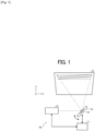
- FIG. 1 illustrates an exemplary schematic diagram of the optical scanning system.
- the optical scanning system 10 deflects light emitted from a light source 12 in accordance with the control of a driving device 11, with a reflection plane 14 included in a light deflector 13, so as to optically scan a to-be-scanned surface 15.
- the optical scanning system 10 includes the driving device 11, the light source 12, and the light deflector 13 including the reflection plane 14.
- the driving device 11 includes, for example, an electronic circuit unit including a central processing unit (CPU) and a field-programmable gate array (FPGA).
- the light deflector 13 includes, for example, a micro electromechanical systems (MEMS) device including the reflection plane 14 and capable of moving the reflection plane 14.
- the light source 12 includes, for example, a laser device that emits a laser.
- the to-be-scanned surface 15 includes, for example, a screen.
- the driving device 11 generates a control command for each of the light source 12 and the light deflector 13 on the basis of optical scanning information that has been acquired, so as to output a driving signal to each of the light source 12 and the light deflector 13 on the basis of the control command.
- the light source 12 performs emission of a light source on the basis of the driving signal that has been input.
- the light deflector 13 moves the reflection plane 14 to at least one of a uniaxial direction and a biaxial direction, on the basis of the driving signal that has been input.
- the control of the driving device 11 based on image information being exemplary optical scanning information reciprocates the reflection plane 14 of the light deflector 13 in a predetermined range in the biaxial direction. Then, the light incident on the reflection plane 14, the light being emitted from the light source 12, is deflected to perform the optical scanning so that an arbitrary image can be projected onto the to-be-scanned surface 15.
- FIG. 2 is a diagram of the exemplary hardware configuration of the optical scanning system 10.
- the optical scanning system 10 includes the driving device 11, the light source 12, and the light deflector 13, electrically coupled to each other.
- the driving device 11 includes a CPU 20, a random access memory (RAM) 21, a read only memory (ROM) 22, an FPGA 23, an external interface (I/F) 24, a light source driver 25, and a light deflector driver 26.
- the CPU 20 includes an arithmetic device that reads a program and data from a storage device, such as the ROM 22, onto the RAM 21 and performs processing to achieve the control and function of the entire driving device 11.
- the RAM 21 includes a volatile storage device that temporarily retains a program and data.
- the ROM 22 includes a nonvolatile storage device capable of retaining a program and data even when power is turned off, and stores a processing program and data executed by the CPU 20 to control each function of the optical scanning system 10.
- the FPGA 23 includes a circuit that outputs a control signal suitable for each of the light source driver 25 and the optical deflector driver 26 in accordance with the processing of the CPU 20.
- the external I/F 24 includes an interface with, for example, an external device or a network.
- the external device include a host device, such as a personal computer (PC), storage devices, such as a universal serial bus (USB) memory, a secure digital (SD) card, a compact disc (CD), a digital versatile disc (DVD), a hard disk drive (HDD), and a solid-state drive (SSD).
- the network include a controller area network (CAN) for a motor vehicle, a local area network (LAN), and the Internet.
- CAN controller area network
- the external I/F 24 at least has a configuration capable of allowing connection or communication with the external device, and the external interface 24 may be prepared for each external device.
- the light source driver includes an electric circuit that outputs a driving signal, such as a driving voltage, to the light source 12 in accordance with the control signal that has been input.
- a driving signal such as a driving voltage
- the light deflector driver 26 includes an electric circuit that outputs a driving signal, such as a driving voltage, to the light deflector 13 in accordance with the control signal that has been input.
- a driving signal such as a driving voltage
- the CPU 20 acquires optical scanning information from the external device or the network through the external interface 24.
- a configuration in which the CPU 20 can acquire the optical scanning information is at least provided.
- the ROM 22 or the FPGA 23 in the driving device 11 may be configured to store the optical scanning information.
- an additional storage device such as an SSD, may be provided in the driving device 11 so that the storage device may be configured to store the optical scanning information.
- the optical scanning information includes information indicating how the optical scanning is performed to the to-be-scanned surface 15.
- the optical scanning information includes image data.
- the optical scanning information includes writing data indicating a writing order or a writing place.
- the optical scanning information includes emission data indicating timing with which light for the object recognition is emitted and an emission range.
- the driving device 11 can achieve a functional configuration to be described next, with the command of the CPU 20 and the hardware configuration illustrated in FIG. 2 .
- FIG. 3 is an exemplary functional block diagram of the driving device 11 of the optical scanning system 10.
- the driving device 11 has the functions of a control unit 30 and a driving signal output unit 31.
- the control unit 30 is achieved with, for example, the CPU 20 and the FPGA 23.
- the control unit 30 acquires the optical scanning information from the external device and converts the optical scanning information into a control signal to output the control signal to the driving signal output unit 31.
- the control unit 30 is included in a control means.
- the control unit 30 acquires image data as the optical scanning information from the external device and generates a control signal from the image data with predetermined processing to output the control signal to the driving signal output unit 31.
- the driving signal output unit 31 is achieved with the light source driver 25 and the light deflector driver 26, and is included in an application means.
- the driving signal output unit 31 outputs a driving signal to the light source 12 or the light deflector 13 on the basis of the control signal that has been input.
- the driving signal output unit 31 (the application means) may be provided for each object to which outputting the driving signal.
- the driving signal includes a signal for controlling the driving of the light source 12 or the light deflector 13.
- the signal includes a driving voltage for controlling the emission timing and the emission intensity of the light source.
- the signal includes a driving voltage for controlling the timing of moving the reflection plane 14 included in the light deflector 13 and the movable range.
- the driving device 11 may acquire the emission timing of the light source and light-receiving timing from the light source 12 and an external device, such as a light-receiving device, respectively, so as to synchronize the pieces of timing with the driving of the light deflector 13.
- FIG. 4 is an exemplary flowchart of the processing according to the optical scanning system 10.
- the control unit 30 acquires optical scanning information from, for example, an external device.
- the control unit 30 generates a control signal from the acquired optical scanning information, and outputs the generated control signal to the driving signal output unit 31.
- the driving signal output unit 31 outputs a driving signal to each of the light source 12 and the light deflector 13, based on the input control signal.
- the light source 12 emits light based on the input driving signal.
- the light deflector 13 moves the reflection plane 14 on the basis of the driving signal that has been input.
- the driving of the light source 12 and the driving of the light deflector 13, deflect the light in an arbitrary direction so that the optical scanning is performed.
- the optical scanning system 10 includes one number of the driving device 11 including a device that controls the light source 12 and the light deflector 13, with the function, but a driving device for the light source 12 and a driving device for the light deflector 13 may be separately provided.
- the optical scanning system 10 includes one number of the driving device 11 including the function of the control unit 30 and the function of the driving signal output unit 31 provided for the light source 12 and the light deflector 13.
- the functions may be individually present, and thus, for example, a driving signal output device including the driving signal output unit 31 may be separately provided from the driving device 11 including the control unit 30.
- the light deflector 13 including the reflection plane 14 and the driving device 11 in the optical scanning system 10 may be included in an optical deflection system that performs optical deflection.
- FIGS. 5 and 6 An image projection device to which the driving device according to the present embodiment has been applied, will be described in detail referring to FIGS. 5 and 6 .
- FIG. 5 is a schematic diagram of a motor vehicle 400 including a mobile object equipped with an exemplary head-up display device 500 of the image projection device, according to the embodiment.
- FIG. 6 is an exemplary schematic diagram of the head-up display device 500.
- the image projection device includes a device that projects an image with optical scanning, and includes, for example, a head-up display device.
- the head-up display device 500 is installed, for example, in the vicinity of a windshield (e.g., a windshield 401) of the motor vehicle 400. Projection light L emitted from the head-up display device 500 is reflected by the windshield 401 so as to travel to an observer (a driver 402) being a user.
- a windshield e.g., a windshield 401
- Projection light L emitted from the head-up display device 500 is reflected by the windshield 401 so as to travel to an observer (a driver 402) being a user.
- the driver 402 can visually recognize an image projected by the head-up display device 500 as a virtual image.
- a configuration in which a combiner is mounted on an inner wall surface of the windshield to allow the user to visually recognize a virtual image with projection light reflected by the combiner may be provided.
- pieces of laser light are emitted from red, green, and blue laser light sources 501R, 501G, and 501B in the head-up display device 500.
- the pieces of laser light that have been emitted travel through incidence optical system including collimator lenses 502, 503, and 504 provided for the respective laser light sources, two dichroic mirrors 505 and 506, and a light amount adjusting unit 507, and then the pieces of laser light are deflected by the light deflector 13 including the reflection plane 14.
- the pieces of laser light that have been deflected are projected on a screen through a projection optical system including a free-form surface mirror 509, an intermediate screen 510, and a projection mirror 511.
- the laser light sources 501R, 501G, and 501B, the collimator lenses 502, 503, and 504, and the dichroic mirrors 505 and 506 are unitized in an optical housing as a light source unit 530.
- the head-up display device 500 projects an intermediate image displayed on the intermediate screen 510, onto the windshield 401 of the motor vehicle 400, so that the driver 402 visually recognizes the intermediate image as a virtual image.
- the collimator lenses 502, 503, and 504 convert the pieces of color laser light emitted from the laser light sources 501R, 501G, and 501B into pieces of substantially collimated light, respectively, and the two dichroic mirrors 505 and 506 synthesize the pieces of substantially collimated light.
- the light deflector 13 including the reflection plane 14 performs two-dimensional scanning with the pieces of laser light.
- the projection light L with which the two-dimensional scanning has been performed by the light deflector 13 is reflected by the free-form surface mirror 509 so that the distortion of the projection light L is corrected.
- the intermediate screen 510 includes a microlens array including microlenses two-dimensionally arranged, and magnifies the projection light L incident on the intermediate screen 510, in units of microlenses.
- the light deflector 13 reciprocates the reflection plane 14 in the biaxial direction so as to perform the two dimensional scanning with the projection light L incident on the reflection plane 14.
- the control of the driving of the light deflector 13 is performed in synchronization with the light emission timing of the laser light sources 501R, 501G, and 501B.
- the exemplary head-up display device 500 of the image projection device has been described above, but the image projection device at least includes a device that performs optical scanning with the light deflector 13 including the reflection plane 14 to project an image.
- the image projection device can be similarly applied to, for example, a projector that projects an image onto a display screen, the projector being on a desk, or a head-mounted display device that is mounted on a wearing member to be worn on the head of an observer to perform projection onto a reflective and transmissive screen included in the wearing member or to project an image onto an eyeball as a screen.
- the image projection device may be mounted on, for example, a mobile object, such as an aircraft, a vessel, or a mobile robot, or non-mobile object, such as a working robot that operates an object to be driven, such as a manipulator, the working robot not moving from the place, in addition to a vehicle and a wearing member.
- a mobile object such as an aircraft, a vessel, or a mobile robot
- non-mobile object such as a working robot that operates an object to be driven, such as a manipulator, the working robot not moving from the place, in addition to a vehicle and a wearing member.
- FIG. 7 illustrates an exemplary image forming apparatus including the optical writing device 600 incorporated.
- FIG. 8 is an exemplary schematic diagram of the optical writing device 600.
- the optical writing device 600 is used as a constituent member of the image forming apparatus typified by a laser printer 650 having a printer function with laser light.
- the optical writing device 600 performs optical scanning to a photoconductor drum being the to-be-scanned surface 15 with one or a plurality of laser beams, so as to perform optical writing onto the photoconductor drum.
- the laser light from the light source 12, such as a laser element travels through an imaging forming optical system 610, such as a collimator lens, and then the light deflector 13 including the reflection plane 14 deflects the laser light in the uniaxial direction or the biaxial direction.
- an imaging forming optical system 610 such as a collimator lens
- the laser light that has been deflected by the light deflector 13 travels through a scanning optical system 620 including a first lens 620a, a second lens 620b, and a reflecting mirror 620c, and then the to-be-scanned surface 15 (e.g., the photoconductor drum or photosensitive paper) is irradiated with the laser light so that the optical writing is performed.
- the scanning optical system 620 forms the image of a light beam in a spot shape on the to-be-scanned surface 15.
- the light source 12 and the light deflector 13 including the reflection plane 14 are driven on the basis of the control of the driving device 11.
- the optical writing device 600 can be used as the constituent member of the image forming apparatus having the printer function with the laser light.
- Changing the scanning optical system and allowing the optical scanning not only in the uniaxial direction but also in the biaxial direction can use the optical writing device as a constituent member of an image forming apparatus, such as a laser labeling device that performs optical scanning and heating with laser light being deflected onto a thermal medium so as to make printing.
- the light deflector 13 including the reflection plane 14, to be applied to the optical writing device is smaller than a rotary polygon mirror using a polygon mirror, in power consumption for driving, so that power saving of the optical writing device is advantageous to achieve.
- Wind noise in oscillating the light deflector 13 is smaller than the wind noise of the rotary polygon mirror so that the optical writing device is advantageous to improve in quietness.
- the optical writing device requires less installation space than the rotary polygon mirror and the amount of heat generated by the light deflector 13 is also small, so that miniaturization is easy to perform.
- the image forming apparatus is advantageous to miniaturize.
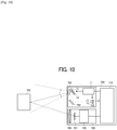
- FIGS. 9 and 10 An object recognition device to which the driving device according to the present embodiment has been applied, will be described in detail referring to FIGS. 9 and 10 .
- FIG. 9 is a schematic diagram of a motor vehicle equipped with an exemplary light detection and ranging (LiDAR) device of the object recognition device.
- FIG. 10 is an exemplary schematic diagram of the LiDAR device.
- the object recognition device recognizes an object in a target direction and, for example, includes the LiDAR device.
- the LiDAR device 700 is mounted on, for example, the motor vehicle 701, and performs optical scanning in the target direction to receive reflected light from an object to be recognized 702 present in the target direction so that the object to be recognized 702 is recognized.
- laser light emitted from the light source 12 travels through an incidence optical system including a collimator lens 703 being an optical system that converts divergent light into substantially collimated light, and a plane mirror 704, and then the light deflector 13 including the reflection plane 14 performs scanning with the laser light in the uniaxial direction or in the biaxial direction. Then, the laser light travels through a projection lens 705 being a projection optical system and then the object to be recognized 702 ahead of the device is irradiated with the laser light.
- the driving device 11 controls the driving of the light source 12 and the driving of the light deflector 13.
- the reflected light reflected by the object to be recognized 702 is photo-detected by a photodetector 709.
- the reflected light is received by an image pickup device 707 through a condenser lens 706 being a light receiving optical system, and then the image pickup device 707 outputs a detected signal to a signal processing circuit 708.
- the signal processing circuit 708 performs predetermined processing, such as binarization and noise processing, to the detected signal that has been input, so as to output a result to a range-finding circuit 710.
- the range-finding circuit 710 recognizes whether the object to be recognized 702 is present, with the time difference between timing at which the light source 12 emits the laser light and timing at which the photodetector 709 receives the laser light or with a phase difference for each pixel in the image pickup device 707 that has received the laser light, and further calculates distance information on the object to be recognized 702.
- the light deflector 13 including the reflection plane 14 is harder to break and smaller in size than a polygon mirror so that a compact LiDAR device having high durability can be provided.
- Such a LiDAR device is attached to, for example, a vehicle, an aircraft, a vessel, or a robot, and can recognize whether an obstacle is present or a distance to the obstacle, while performing optical scanning in a predetermined range.
- the object recognition device has been described with the exemplary LiDAR device 700.
- the object recognition device at least includes a device that controls the light deflector 13 including the reflection plane 14 with the driving device 11 to perform optical scanning and then receives reflected light with a photodetector to recognize the object to be recognized 702.
- the object recognition device is not limited to the device according to the embodiment described above.
- the object recognition device can be similarly applied to a constituent member for biometric authentication that calculates object information on a shape from distance information acquired by performing optical scanning to a hand or a face and then recognizes the object referring to a record, a security sensor that recognizes an intruding object with optical scanning in a target range, or a three-dimensional scanner that calculates object information on a shape, from distance information acquired by optical scanning to perform recognition and then outputs the object information as three-dimensional data.
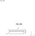
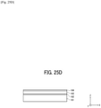
- FIG. 11 is an exemplary schematic diagram of the light deflector 13 that has been packaged.
- the light deflector 13 is attached to an attaching member 801 arranged inside a package member 802 being a housing. Then, a portion of the package member 802 is covered with a transmissive member 803 so as to be hermetically sealed so that the light deflector 13 is packaged.
- an inert gas such as nitrogen
- an inert gas such as nitrogen
- FIG. 12 is a plan view of the light deflector being dual-typed, the light deflector being capable of performing optical deflection in the biaxial direction including an X direction being a main-scanning direction and a Y direction being a sub-scanning direction.
- FIG. 13 is a cross-sectional view taken along line P-P' of FIG. 12 .
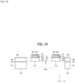
- FIG. 14 is a cross-sectional view taken along line Q-Q' of FIG. 12 .
- a direction in which a bundle of the light L reflected by the reflection plane 14 moves when the reflection plane 14 is driven around a first axis O 1 as to be described later is defined as the main-scanning direction X
- a direction in which the bundle of the light L moves when the reflection plane 14 is driven around a second axis O 2 is defined as the sub-scanning direction Y.
- the main-scanning direction and the sub-scanning direction are not limited to the configuration, and thus the main-scanning direction and the sub-scanning direction may be appropriately changed in accordance with a configuration.
- the light deflector 13 includes a mirror unit 101 being the reflection plane that reflects the light L that has been incident, and first driving units 110a and 110b coupled to the mirror unit 101, the first driving units 110a and 110b configured to drive the mirror unit 101 around the first axis O 1 parallel to the Y axis.
- the light deflector 13 also includes a first supporting unit 120 being a supporting member supporting the mirror unit 101 and the first driving units 110a and 110b.
- the light deflector 13 also includes second driving units 130a and 130b coupled to the first supporting unit 120, the second driving units 130a and 130b configured to drive the mirror unit 101 and the first supporting unit 120 around the second axis O 2 parallel to the X axis, and a second supporting unit 140 being a frame body supporting the second driving units 130a and 130b.
- first driving units 110a and 110b, the mirror unit 101, and the first supporting unit 120 according to the present example are included in a movable unit that turns around the second axis O 2 .
- the second driving units 130a and 130b support the movable unit with respect to the second supporting unit 140.
- the first driving units 110a and 110b are coupled to the first supporting unit 120 being a supporting unit formed so as to surround the mirror unit 101.
- the second driving units 130a and 130b are coupled to the second supporting unit 140 being a supporting unit formed so as to surround the mirror unit 101 and the first supporting unit 120.
- the light deflector 13 includes an electrode connector 150 and a conduction path 151, the electrode connector 150 being electrically coupled to the first driving units 110a and 110b, the second driving units 130a and 130b, and the driving device, the conduction path 151 extending from the electrode connector 150 to the first driving units 110a and 110b.
- the light deflector 13 includes the reflection plane 14, first piezoelectric driving units 112a and 112b, second piezoelectric driving units 131a to 131f and 132a to 132f, and the electrode connector 150 integrally formed on a substrate including one silicon on insulator (SOI) substrate to which forming has been performed with etching processing.
- SOI silicon on insulator
- the formation of each of the constituent elements may be performed after the forming of the SOI substrate or during the forming of the SOI substrate.
- the SOI substrate includes a silicon substrate including a silicon supporting layer 161 as a base material layer being a first silicon layer including, for example, single crystal silicon (Si), a silicon oxide layer 162 on the silicon supporting layer 161, and a silicon active layer 163 being a second silicon layer on the silicon oxide layer 162.
- a silicon substrate including a silicon supporting layer 161 as a base material layer being a first silicon layer including, for example, single crystal silicon (Si), a silicon oxide layer 162 on the silicon supporting layer 161, and a silicon active layer 163 being a second silicon layer on the silicon oxide layer 162.
- a member including the silicon active layer 163 has a function as an elastic member having elasticity.
- the second driving units 130a and 130b and the first driving units 110a and 110b each have the silicon active layer 163 as a base material and thus have the function as the elastic member.
- “having the elasticity” or “having the function as the elastic member” means having restoring force against deformation of a piezoelectric unit 202 to be described later.
- the SOI substrate does not necessarily have a planar shape, and thus may have curvature.
- the member used for the formation of the light deflector 13 is not limited to the SOI substrate as long as a substrate to which integrally forming can be performed with the etching processing, the substrate being capable of partially having elasticity, is provided.
- the mirror unit 101 includes, for example, a mirror base 102 having a disk shape and the reflection plane 14 on the surface of the mirror base 102 on the +Z side.
- the mirror base 102 includes, for example, the silicon active layer 163.
- the reflection plane 14 includes, for example, a metal thin film containing aluminum, gold, or silver.
- the mirror unit 101 may include a rib for reinforcing the mirror unit 101, on the surface of the mirror base 102 on the -Z side.
- the rib includes, for example, the silicon supporting layer 161 and the silicon oxide layer 162, and can inhibit the reflection plane 14 from being distorted by the operation of the mirror unit 101.
- the first driving units 110a and 110b include two torsion bars 111a and 111b and the first piezoelectric driving units 112a and 112b, the two torsion bars 111a and 111b extending in a first axis direction to movably support the mirror unit 101, one end of each of the torsion bars 111a and 111b being coupled to the mirror base 102, the first piezoelectric driving units 112a and 112b each having one end coupled to the torsion bar and the other end coupled to an inner periphery of the first supporting unit 120, respectively.
- the torsion bars 111a and 111b each include the silicon active layer 163.
- the first piezoelectric driving units 112a and 112b each include sequentially a lower electrode 201, the piezoelectric unit 202, and an upper electrode 203 on the surface of the silicon active layer 163 on the +Z side.
- the upper electrode 203 and the lower electrode 201 each include, for example, gold (Au) or platinum (Pt).
- the piezoelectric unit 202 includes, for example, lead zirconate titanate (PZT) being a piezoelectric material.
- the first supporting unit 120 includes a rectangular support formed to surround the mirror unit 101, the rectangular support including the silicon supporting layer 161, the silicon oxide layer 162, and the silicon active layer 163.
- an insulating layer 164 e.g., a silicon oxide layer may be provided on the silicon active layer 163 in order to avoid electrical connection with the lower electrode 201.
- the first supporting unit 120 includes a thin portion 602 formed by etching the silicon supporting layer 161, the thin portion 602 including the silicon active layer 163 having a thickness of 30 ⁇ m and the insulating layer 164, and a thick portion 601 having a three-layer laminated structure including the silicon active layer 163, the silicon oxide layer 162, and the silicon supporting layer 161, the thick portion 601 being a plate-shaped or columnar bone member having a total thickness of 300 ⁇ m.
- FIGS. 15(b) to 15E are cross-sectional views taken along lines A-A', B-B', C-C', and D-D' of FIG. 15A , respectively.
- the thick portion 601 is formed so as to divide the thin portion 602 as illustrated in the cross-sectional views viewed in the respective directions in FIGS. 15(b) to 15E . That is, the thick portion 601 forms the frame structure of the first supporting unit 120. Note that, here, the frame structure indicates a mode in which the thick portion 601 functions as a beam so as to reinforce the rigidity that has degraded due to so-called "hollowing out”.
- the rigidity of the first supporting unit 120 is lower than the rigidity of a simple plate-shaped member having a thickness of 300 ⁇ m so that the first supporting unit 120 easily deforms.
- the thick portion 601 reinforces the rigidity in the degree in which breaking due to the deformation barely occurs.
- the frame structure including the thick portion 601 having the plate shape parallel to the X direction being an oscillation direction of the mirror unit 101 (namely, the main-scanning direction) and the thick portion 601 having the plate shape perpendicular to the X direction, combined, is provided.
- the frame structure is not limited to the configuration, and thus may include, for example, a plurality of the thick portions 601 having the plate shape, combined to cross each other.
- FIG. 16 illustrates a comparison in amount of warpage between the present invention and a related art example in which formation is made with a simple plate-like SOI substrate, as will be described later with reference to FIG. 25A to FIG. 25E .
- the warpage according to the related art example is 0.12 ⁇ m
- the warpage after forming per length of 2.5 mm is 0.24 ⁇ m larger in the first supporting unit 120 according to the present example. This can be considered to be due to stress occurring in removing the silicon supporting layer 161.
- the thick portion 601 and the thin portion 602 are excluded from a configuration similar to the configuration according to the first example, the same reference signs are given in notation according to the related art example in FIG. 25 . Thus the descriptions will be appropriately omitted.
- the first supporting unit 120 has elastic force so as to retain the state where the deformation more easily occurs in comparison to the case where the simple plate-shaped member is used.
- the amount of displacement of the mirror unit 101 is in a unit of at least several tens ⁇ m, the influence of the warpage due to the stress, on the oscillation of the mirror unit 101, can be considered to be sufficiently small.
- the second driving units 130a and 130b include the plurality of second piezoelectric driving units 131a to 131f and 132a to 132f coupled so as to be folded back, respectively.
- One end of each of the second driving units 130a and 130b is coupled to an outer periphery of the first supporting unit 120 and the other end is coupled to an inner periphery of the second supporting unit 140.
- a coupling portion between the second driving unit 130a and the first supporting unit 120, a coupling portion between the second driving unit 130b and the first supporting unit 120, a coupling portion between the second driving unit 130a and the second supporting unit 140, and a coupling portion between the second driving unit 130b and the second supporting unit 140 may be point-symmetric with respect to the center of the reflection plane 14.
- the second piezoelectric driving units 131a and 131b each include sequentially the lower electrode 201, the piezoelectric unit 202, and the upper electrode 203 on the surface of the silicon active layer 163 on the +Z side.
- the upper electrode 203 and the lower electrode 201 each include, for example, gold (Au) or platinum (Pt).
- the piezoelectric unit 202 includes, for example, a piezoelectric member including lead zirconate titanate (PZT) being a piezoelectric material.
- the second supporting unit 140 includes, for example, a rectangular support formed to surround the mirror unit 101, the first driving units 110a and 110b, the first supporting unit 120, and the second driving units 130a and 130b, the rectangular support including the silicon supporting layer 161, the silicon oxide layer 162, and the silicon active layer 163.
- the electrode connector 150 is formed, for example, on the surface of the second supporting unit 140 on the +Z side, and is electrically coupled to the first piezoelectric driving units 112a and 112b, the respective upper electrodes 203 and the respective lower electrodes 201 of the second piezoelectric driving units 131a to 131f, and the driving device 11 illustrated in FIG. 1 through an electrode conductive line, such as aluminum (Al).
- an electrode conductive line such as aluminum (Al).
- the upper electrode 203 or the lower electrode 201 may be directly coupled to the electrode connector 150 or may be indirectly coupled with coupling between the electrodes.
- the piezoelectric unit 202 may be provided on the other surface of the elastic member (e.g., the surface on the -Z side) or may be provided on both of the one surface and the other surface of the elastic member.
- each of the constituent elements is not limited to the shape according to the example as long as the mirror unit 101 can be driven around the first axis or the second axis.
- the torsion bars 111a and 111b and the first piezoelectric driving units 112a and 112b each may have a shape with curvature.
- an insulating layer including a silicon oxide film may be formed on at least one of the surface of the upper electrode 203 of each of the first driving units 110a and 110b on the +Z side, the surface of the first supporting unit 120 on the +Z side, the surface of the upper electrode 203 of each of the second driving units 130a and 130b on the +Z side, and the surface of the second supporting unit 140 on the +Z side.
- an electrode conductive line is provided on the insulating layer, and the insulating layer is partially removed or no insulating layer is formed for an opening at a coupling spot at which the upper electrode 203 or the lower electrode 201 and the electrode conductive line are coupled to each other.
- the degree of freedom in designing the first driving units 110a and 110b, the second driving units 130a and 130b, and the electrode conductive line increases so that a short circuit due to a contact between the electrodes can be further inhibited.
- the insulating layer as least includes a member having an insulating property and additionally may have a function as an antireflective material.
- first driving units 110a and 110b and the second driving units 130a and 130b When a positive or negative voltage is applied in the polarization direction of the piezoelectric unit 202 included in each of the first driving units 110a and 110b and the second driving units 130a and 130b, deformation (e.g., expansion and contraction) proportional to the potential of the voltage that has been applied, occurs so that a so-called inverse piezoelectric effect is exerted.
- the first driving units 110a and 110b and the second driving units 130a and 130b move the mirror unit 101 with the reverse piezoelectric effect.
- the angle at which a bundle of light incident on the reflection plane 14 of the mirror unit 101 is deflected is called a deflection angle.
- the deflection angle when no voltage is applied to the piezoelectric unit 202 is defined as zero.
- the deflection angle larger than the angle of zero, is defined as a positive deflection angle, and the deflection angle smaller than the angle of zero, is defined as a negative deflection angle.
- the control of the driving device 11 that drives the first driving units 110a and 110b will be described.
- the first driving units 110a and 110b when a driving voltage is applied in parallel to the piezoelectric units 202 included in the first piezoelectric driving units 112a and 112b through the upper electrodes 203 and the lower electrodes 201, each of the piezoelectric units 202 deforms. Due to the deformation of the piezoelectric units 202, the first piezoelectric driving units 112a and 112b bend and deform. As a result, driving force around the first axis acts on the mirror unit 101 through the torsion of each of the two torsion bars 111a and 111b so that the mirror unit 101 moves around the first axis.
- the driving voltage applied to the first driving units 110a and 110b is controlled by the driving device 11.
- the driving device 11 applies the driving voltage having a predetermined sinusoidal waveform, in parallel to the first piezoelectric driving units 112a and 112b included in the first driving units 110a and 110b so that the mirror unit 101 can move around the first axis O 1 in the cycle of the driving voltage having the predetermined sinusoidal waveform.
- the mirror unit 101 can resonantly oscillate at a frequency of approximately 20 kHz with the occurrence of mechanical resonance due to the torsion of each of the torsion bars 111a and 111b.
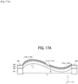
- the light deflector including the first piezoelectric driving units 112a and 112b having a length of Li and a deflection angle of ⁇ 1 , the first piezoelectric driving units 112a and 112b each being a cantilever.
- the first piezoelectric driving units 112a and 112b each expand and contract in accordance with a voltage to be applied, the first piezoelectric driving units 112a and 112b each including one end secured to the first supporting unit 120.
- the displacements h 1 and h 2 of the ends in FIGS. 17A and 17B are different from each other, and the following expression is assumed to be satisfied: hi ⁇ 4h 2 for a doubly supported beam structure.
- reducing the lengths of the first piezoelectric driving units 112a and 112b, namely, miniaturizing the first piezoelectric driving units 112a and 112b, generally decreases a scanning angle ⁇ being the deflection angle of the mirror unit 101.
- the scanning angle ⁇ varies in accordance with the voltage applied to the piezoelectric units 202.
- the voltage to be applied at least increases in order to retain the scanning angle ⁇ with the miniaturization performed.
- increasing the applied voltage after the miniaturization is likely to cause an unintended failure, such as a short circuit.
- the mirror unit 101 including the reflection plane 14, the mirror unit 101 configured to turn around the predetermined rotational axis O 1 , a pair of the torsion bars 111a and 111b rotatably supporting the mirror unit 101, and the first piezoelectric driving units 112a and 112b configured to drive the mirror unit 101 to turn, through the torsion bars 111a and 111b.
- the first piezoelectric driving units 112a and 112b have the one ends coupled to the torsion bars 111a and 111b and the other ends coupled to the first supporting unit 120 formed to surround the mirror unit 101.
- the first supporting unit 120 includes the thick portion 601 and the thin portion 602 at least partially different from each other in thickness.
- the thin portion 602 deforms so that the first supporting unit 120 easily deforms, in other words, the first supporting unit 120 deforms with elasticity improved.
- the scanning angle ⁇ is retained with the voltage retained even in miniaturizing the light deflector 13.
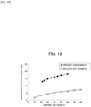
- the scanning angle ⁇ As a result of measurement of the scanning angle ⁇ , it is found that the scanning angle ⁇ more improves than the scanning angle according to the related art example as illustrated in FIG. 19 .
- the amount of oscillation by the first supporting unit 120 is improved compared with the amount of oscillation in the related art example.
- an amount of oscillation in the mirror unit 101 is adjusted in the same manner as the related art example as illustrated in FIG. 20A so that the amount of oscillation of the first supporting unit 120 at that time is illustrated as an amount of oscillation according to the present example.
- the numbers of points illustrated in FIGS. 20A and 20B indicate amount of oscillations at positions PI to P7 illustrated in FIG. 20C .
- FIGS. 21A and 21B are schematic views of the driving of each of the second driving units 130a and 130b of the light deflector 13. An area indicated with hatching is the mirror unit 101.
- the second piezoelectric driving unit having an even number counted from the second piezoelectric driving unit (131a) having the shortest distance from the mirror unit 101, namely, the second piezoelectric driving units 131b, 131d and 131f are defined as a piezoelectric driving unit group A.
- the second piezoelectric driving unit having an odd number counted from the second piezoelectric driving unit (132a) having the shortest distance from the mirror unit 101 namely, the second piezoelectric driving units 132a, 132c, and 132e are similarly defined as the piezoelectric driving unit group A.
- the piezoelectric driving unit group A bends and deforms in the same direction so that the mirror unit 101 moves around the second axis O 2 to have a positive deflection angle.
- the second piezoelectric driving unit having an odd number counted from the second piezoelectric driving unit (131a) having the shortest distance from the mirror unit 101, namely, the second piezoelectric driving units 131a, 131c, and 131e are defined as a piezoelectric driving unit group B.
- the second piezoelectric driving unit having an even number counted from the second piezoelectric driving unit (132a) having the shortest distance from the mirror unit 101 namely, the second piezoelectric driving units 132b, 132d and 132f are similarly defined as the piezoelectric driving unit group B.
- the piezoelectric driving unit group B bends and deforms in the same direction so that the mirror unit 101 moves around the second axis O 2 to have a negative deflection angle.
- the second driving units 130a and 130b bend the plurality of piezoelectric units 202 included in the piezoelectric driving unit group A or the plurality of piezoelectric units 202 included in the piezoelectric driving unit group B, so as to accumulate a movable amount due to the bend and the deformation.
- the deflection angle of the mirror unit 101 around the second axis can increase.
- the second driving units 130a and 130b are point-symmetrically coupled to the first supporting unit 120 with respect to the center point of the first supporting unit 120. Therefore, when the driving voltage is applied to the piezoelectric driving unit group A, driving force that moves the connector between the first supporting unit 120 and the second driving unit 130a in a + Z direction, occurs in the second driving unit 130a, and driving force that moves the connector between the first supporting unit 120 and the second driving unit 130b in a -Z direction, occurs in the second driving unit 130b.
- a movable amount is accumulated so that the deflection angle of the mirror unit 101 around the second axis can increase.
- applying the driving voltage to the second piezoelectric driving units to continuously repeat the states in FIG. 21A and FIG. 21B can drive the mirror unit 101 around the second axis O 2 .
- the driving voltage applied to the second drive units is controlled by the driving device.
- the driving voltage applied to the piezoelectric driving unit group A (hereinafter, referred to as a driving voltage A) and the driving voltage applied to the piezoelectric driving unit group B (hereinafter, referred to as a driving voltage B), will be described referring to FIGS. 22A to 22C .
- An application means that applies the driving voltage A (a first driving voltage) is referred to as a first application means
- an application means that applies the driving voltage B (a second driving voltage) is referred to as a second application means.
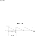
- FIG. 22A illustrates an exemplary waveform of the driving voltage A applied to the piezoelectric driving unit group A of the light deflector.
- FIG. 22B illustrates an exemplary waveform of the driving voltage B applied to the piezoelectric driving unit group B of the light deflector.
- FIG. 22C is a graph illustrating the waveform of the driving voltage A and the waveform of the driving voltage B superimposed.
- the waveform of the driving voltage A applied to the piezoelectric driving unit group A includes, for example, a sawtooth waveform with a frequency of 60 Hz.
- TrA time width of a rising period during which a voltage value increases from the minimum value to the next maximum value
- TfA time width of a falling period during which the voltage value decreases from the maximum value to the next minimum value
- the waveform of the driving voltage B applied to the piezoelectric driving unit group B includes, for example, a sawtooth waveform with a frequency of 60 Hz.
- TrB time width of a rising period during which a voltage value increases from the minimum value to the next maximum value
- TfB time width of a falling period during which the voltage value decreases from the maximum value to the next minimum value
- the ratio of TfB to one cycle is referred to as the symmetry of the driving voltage B.
- the cycle TA of the waveform of the driving voltage A and the cycle TB of the waveform of the driving voltage B are set to be the same.
- the sawtooth waveforms of the driving voltage A and the driving voltage B are generated by, for example, superimposing sinusoidal waves.
- driving voltages having the sawtooth waveforms have been used as the driving voltages A and B.
- the driving voltages A and B are not limited to the driving voltages, and thus the waveforms of the driving voltages A and B each can be changed in accordance with a device characteristic of the light deflector, for example, a driving voltage having a waveform including the peaks of a sawtooth waveform rounded or a driving voltage having a waveform including the linear areas of a sawtooth waveform curved.
- the symmetry is the ratio of rising time to one cycle or the ratio of falling time to the one cycle. At this time, which of the rising time and the falling time is used as a reference, may be arbitrarily set.
- the first supporting unit 120 has the laminated structure including the silicon supporting layer 161 being the base material layer and the silicon active layer 163 being an active layer.
- the thin portion 602 includes the silicon active layer 163.
- the elasticity in the first supporting unit 120 improves so that the first supporting unit 120 more easily deforms than the support having the simple plate shape according to the related art example, resulting in the deflection angle increasing in the same condition.
- the light deflector 13 includes the plurality of first driving units 110a and 110b symmetrically arranged to each other with the torsion bars 111a and 111b interposed.
- the first driving units 110a and 110b are arranged so as to be orthogonal to the torsion bars 111a and 111b, respectively.
- the first driving units 110a and 110b twist the torsion bars 111a and 111b from both sides. Since the force perpendicularly acts on the torsion bars 111a and 111b, the deflection angle more easily increases.
- the first supporting unit 120 includes the thin portion 602 and the thick portion 601 provided, but the second supporting unit 140 may have a similar configuration.
- a first supporting unit 120 includes a thick portion 601, a thin portion 602, and an opening 603 including the thick portion 601 and the thin portion 602 different from each other in thickness.
- the opening 603 includes a rectangular hole formed to penetrate through the first supporting unit 120, and is formed so as to be surrounded by the thick portion 601.
- the opening 603 may be coupled to a side to which no first driving units 110a and 110b are coupled, in the inner periphery of the first supporting unit 120.
- Forming the opening 603 further greatly degrades the rigidity of the first supporting unit 120 in comparison to a case where the thin portion 602 is simply provided. If a frame portion of the first supporting unit 120 and torsion bars 111a and 111b simultaneously move due to the degradation of the rigidity, there is a risk that a torsion angle rather decreases.
- the first supporting unit 120 is required to secure minimum rigidity in order to retain one end of each of the first driving units 110a and 110b.
- first piezoelectric driving units 112a and 112b are formed so as to be orthogonal to a first rotational axis O 1 , in other words, so as to be orthogonal to the torsion bars 111a and 111b.
- first piezoelectric driving units 112a and 112b on the side of the first supporting unit 120 may be secured when the first piezoelectric driving units 112a and 112b expand and contract.
- the rigidity may be relatively high and thus the opening 603 may be provided to two sides to which no first piezoelectric driving units 112a and 112b have been coupled, among the four sides of the first supporting unit 120 having a rectangular shape.
- the movable range of the mirror unit 101 easily expands so that a scanning angle is retained with a voltage retained even in miniaturizing a light deflector 13.
- a light deflector 13 according to a second modification of the example described above will be described, the light deflector 13 including a thin portion 602 provided to a portion to which first piezoelectric driving units 112a and 112b and a first supporting unit 120 are coupled, in a frame of a first supporting unit 120 as illustrated in FIGS. 24D to 24E .
- the rigidity of the entire first supporting unit 120 decreases, whereas the width of displacement caused when the first piezoelectric driving units 112a and 112b operate, increases since the thin portion 602 is provided to the contact portion with the first piezoelectric driving units 112a and 112b.
- the movable range of a mirror unit 101 easily expands so that a scanning angle is retained with a voltage retained even in miniaturizing the light deflector 13.
- the driving device 11 applies the piezoelectric units with the driving voltage having the waveform constantly having a positive voltage value, but the present invention is not limited to this as long as a configuration in which the piezoelectric units deform when the driving voltage is applied to the piezoelectric units, is provided.
- the driving device 11 may apply the driving voltage having a waveform constantly having a negative voltage value or may apply a positive voltage value and a negative voltage value alternately, to the piezoelectric units.
- the light deflector 13 includes a dual-typed light deflector including the first piezoelectric driving units 112a and 112b extending in the ⁇ X directions from the torsion bars 111a and 111b, respectively, but is not limited to this as long as a configuration in which the reflection plane 14 is moved by the piezoelectric units to which a voltage has been applied, is provided.
- a configuration in which a single-typed light deflector including the first piezoelectric driving units 112a and 112b extending in the + X direction is used, may be provided.
- the optical deflection device 300 with the single light source 12 has been described, but an optical deflection device that uses a plurality of light sources to perform scanning with a plurality of colors, may be provided.
Description
- The present invention relates to a light deflector, an optical scanning device, an image projection device, and a mobile object.
- The following configuration has been known as a light deflector using a micromachining technique. A piezoelectric member is interposed between an upper electrode and a lower electrode. A voltage is applied across the upper and lower electrodes to oscillate a mirror unit to reflect light, and then the light is output as scanning light (e.g., see
Japanese Patent No. 5493735 Japanese Patent No. 5670227 - However, the oscillation angle is determined by the amount of deformation of the piezoelectric member, and thus there is a disadvantage that the oscillation angle is difficult to increase easily.
-
US2009/284818A1 ,US 2007/180672A1 andEP 2 511 749 A1 disclose a piezo-electric mirror devices with a frame formed of parts of two different thicknesses. - The present invention has been made in consideration of the technical problems as above, and an object of the present invention is to increase the scanning angle of a light deflector.
- According to the present invention, there is provided a light deflector as defined in the appended claims. Any aspects, embodiments and examples of the present disclosure which do not fall under the scope of the appended claims do not form part of the invention and are merely provided for illustrative purposes.
- According to the present invention, decreasing the rigidity of at least some of the light deflector, can provide the light deflector that increases the scanning angle.
-
- [
FIG. 1]FIG. 1 is an exemplary schematic diagram of an optical scanning system. - [
FIG. 2] FIG. 2 is a diagram of an exemplary hardware configuration of the optical scanning system. - [
FIG. 3]FIG. 3 is an exemplary functional block diagram of a driving device. - [
FIG. 4]FIG. 4 is an exemplary flowchart of processing according to the optical scanning system. - [
FIG. 5]FIG. 5 is an exemplary schematic diagram of a motor vehicle equipped with a head-up display device. - [
FIG. 6]FIG. 6 is an exemplary schematic diagram of the head-up display device. - [
FIG. 7]FIG. 7 is an exemplary schematic diagram of an image forming apparatus equipped with an optical writing device. - [
FIG. 8]FIG. 8 is an exemplary schematic diagram of the optical writing device. - [
FIG. 9]FIG. 9 is an exemplary schematic diagram of a motor vehicle installed with a light detection and ranging (LiDAR) device. - [
FIG. 10]FIG. 10 is an exemplary schematic diagram of the LiDAR device. - [
FIG. 11]FIG. 11 is an exemplary schematic diagram of the light deflector that has been packaged. - [
FIG. 12]FIG. 12 is a plan view illustrating an exemplary configuration of the light deflector. - [
FIG. 13]FIG. 13 is a cross-sectional view taken along line P-P' of the light deflector illustrated inFIG. 12 . - [
FIG. 14]FIG. 14 is a cross-sectional view taken along line Q-Q' of the light deflector illustrated inFIG. 12 . - [
FIG. 15]FIGS. 15A to 15E are views schematically illustrating a structure of a movable unit of an example light deflector. - [
FIG. 16]FIG. 16 is a graph illustrating a measured result of warpage in a C-C ' cross-section in the configuration illustrated inFIGS. 15A to 15E . - [
FIG. 17 ]FIGS. 17A and17B are views schematically illustrating a decrease in deflection angle caused due to the size of the light deflector. - [
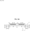
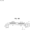
FIG. 18 ]FIGS. 18A and18B are views illustrating exemplary deformation of the light deflector in operation. - [
FIG. 19]FIG. 19 is a graph illustrating a comparison in scanning angle between a light deflector according to the present disclosure and a light deflector according to a related art example. - [
FIG. 20]FIGS. 20A to 20C are graphs and a view illustrating the degree of displacement in a first supporting unit of the example light deflector. - [
FIG. 21 ]FIGS. 21A and21B are views illustrating an exemplary operation of the light deflector. - [
FIG. 22]FIGS. 22A to 22C are graphs each illustrating an exemplary waveform of an applied voltage during the operation of the light deflector. - [
FIG. 23]FIGS. 23A to 23D are views illustrating an exemplary configuration of a light deflector according to the present invention. - [
FIG. 24]FIGS. 24A to 24E are views illustrating an exemplary configuration of a light deflector according to a second modification of the example light deflector. - [
FIG. 25]FIGS. 25A to 25E are views illustrating an exemplary configuration of the light deflector according to the related art example of the present invention. - An embodiment of the present invention will be described in detail below, along with illustrative examples which are outside the scope of the invention.
- First, an optical scanning system to which a driving device according to the embodiment of the present invention has been applied, will be described in detail referring to
FIGS. 1 to 4 . -
FIG. 1 illustrates an exemplary schematic diagram of the optical scanning system. - As illustrated in
FIG. 1 , theoptical scanning system 10 deflects light emitted from alight source 12 in accordance with the control of adriving device 11, with areflection plane 14 included in alight deflector 13, so as to optically scan a to-be-scannedsurface 15. - The
optical scanning system 10 includes thedriving device 11, thelight source 12, and thelight deflector 13 including thereflection plane 14. - The
driving device 11 includes, for example, an electronic circuit unit including a central processing unit (CPU) and a field-programmable gate array (FPGA). Thelight deflector 13 includes, for example, a micro electromechanical systems (MEMS) device including thereflection plane 14 and capable of moving thereflection plane 14. Thelight source 12 includes, for example, a laser device that emits a laser. Note that, the to-be-scannedsurface 15 includes, for example, a screen. - The
driving device 11 generates a control command for each of thelight source 12 and thelight deflector 13 on the basis of optical scanning information that has been acquired, so as to output a driving signal to each of thelight source 12 and thelight deflector 13 on the basis of the control command. - The
light source 12 performs emission of a light source on the basis of the driving signal that has been input. Thelight deflector 13 moves thereflection plane 14 to at least one of a uniaxial direction and a biaxial direction, on the basis of the driving signal that has been input. - With this arrangement, for example, the control of the driving
device 11 based on image information being exemplary optical scanning information, reciprocates thereflection plane 14 of thelight deflector 13 in a predetermined range in the biaxial direction. Then, the light incident on thereflection plane 14, the light being emitted from thelight source 12, is deflected to perform the optical scanning so that an arbitrary image can be projected onto the to-be-scanned surface 15. - Note that, the details of the light deflector and the details of the control of the driving device according to the present embodiment, will be described later.
- Next, an exemplary hardware configuration of the
optical scanning system 10 will be described referring toFIG. 2. FIG. 2 is a diagram of the exemplary hardware configuration of theoptical scanning system 10. As illustrated inFIG. 2 , theoptical scanning system 10 includes the drivingdevice 11, thelight source 12, and thelight deflector 13, electrically coupled to each other. - The driving
device 11 includes aCPU 20, a random access memory (RAM) 21, a read only memory (ROM) 22, anFPGA 23, an external interface (I/F) 24, alight source driver 25, and alight deflector driver 26. - The
CPU 20 includes an arithmetic device that reads a program and data from a storage device, such as theROM 22, onto theRAM 21 and performs processing to achieve the control and function of theentire driving device 11. - The
RAM 21 includes a volatile storage device that temporarily retains a program and data. - The
ROM 22 includes a nonvolatile storage device capable of retaining a program and data even when power is turned off, and stores a processing program and data executed by theCPU 20 to control each function of theoptical scanning system 10. - The
FPGA 23 includes a circuit that outputs a control signal suitable for each of thelight source driver 25 and theoptical deflector driver 26 in accordance with the processing of theCPU 20. - The external I/
F 24 includes an interface with, for example, an external device or a network. Examples of the external device include a host device, such as a personal computer (PC), storage devices, such as a universal serial bus (USB) memory, a secure digital (SD) card, a compact disc (CD), a digital versatile disc (DVD), a hard disk drive (HDD), and a solid-state drive (SSD). Examples of the network include a controller area network (CAN) for a motor vehicle, a local area network (LAN), and the Internet. - The external I/
F 24 at least has a configuration capable of allowing connection or communication with the external device, and theexternal interface 24 may be prepared for each external device. - The light source driver includes an electric circuit that outputs a driving signal, such as a driving voltage, to the
light source 12 in accordance with the control signal that has been input. - The
light deflector driver 26 includes an electric circuit that outputs a driving signal, such as a driving voltage, to thelight deflector 13 in accordance with the control signal that has been input. - In the driving
device 11, theCPU 20 acquires optical scanning information from the external device or the network through theexternal interface 24. Note that, a configuration in which theCPU 20 can acquire the optical scanning information, is at least provided. TheROM 22 or theFPGA 23 in the drivingdevice 11 may be configured to store the optical scanning information. Alternatively, an additional storage device, such as an SSD, may be provided in the drivingdevice 11 so that the storage device may be configured to store the optical scanning information. - Here, the optical scanning information includes information indicating how the optical scanning is performed to the to-
be-scanned surface 15. For example, in a case where the optical scanning displays an image, the optical scanning information includes image data. For example, in a case where the optical scanning performs optical writing, the optical scanning information includes writing data indicating a writing order or a writing place. Besides, for example, in a case where the optical scanning performs object recognition, the optical scanning information includes emission data indicating timing with which light for the object recognition is emitted and an emission range. The drivingdevice 11 according to the present embodiment, can achieve a functional configuration to be described next, with the command of theCPU 20 and the hardware configuration illustrated inFIG. 2 . - Next, the functional configuration of the driving
device 11 in theoptical scanning system 10 will be described referring toFIG. 3. FIG. 3 is an exemplary functional block diagram of the drivingdevice 11 of theoptical scanning system 10. - As illustrated in
FIG. 3 , the drivingdevice 11 has the functions of acontrol unit 30 and a driving signal output unit 31.Thecontrol unit 30 is achieved with, for example, theCPU 20 and theFPGA 23. Thecontrol unit 30 acquires the optical scanning information from the external device and converts the optical scanning information into a control signal to output the control signal to the drivingsignal output unit 31. For example, thecontrol unit 30 is included in a control means. Thecontrol unit 30 acquires image data as the optical scanning information from the external device and generates a control signal from the image data with predetermined processing to output the control signal to the drivingsignal output unit 31. - The driving
signal output unit 31 is achieved with thelight source driver 25 and thelight deflector driver 26, and is included in an application means. The drivingsignal output unit 31 outputs a driving signal to thelight source 12 or thelight deflector 13 on the basis of the control signal that has been input. For example, the driving signal output unit 31 (the application means) may be provided for each object to which outputting the driving signal. - The driving signal includes a signal for controlling the driving of the
light source 12 or thelight deflector 13. For example, in thelight source 12, the signal includes a driving voltage for controlling the emission timing and the emission intensity of the light source. For example, in thelight deflector 13, the signal includes a driving voltage for controlling the timing of moving thereflection plane 14 included in thelight deflector 13 and the movable range. Note that, the drivingdevice 11 may acquire the emission timing of the light source and light-receiving timing from thelight source 12 and an external device, such as a light-receiving device, respectively, so as to synchronize the pieces of timing with the driving of thelight deflector 13. - Next, processing of the optical scanning to the to-
be-scanned surface 15 by theoptical scanning system 10 will be described referring toFIG. 4. FIG. 4 is an exemplary flowchart of the processing according to theoptical scanning system 10. - At step S11, the
control unit 30 acquires optical scanning information from, for example, an external device.At step S12, thecontrol unit 30 generates a control signal from the acquired optical scanning information, and outputs the generated control signal to the drivingsignal output unit 31. - At step S13, the driving
signal output unit 31 outputs a driving signal to each of thelight source 12 and thelight deflector 13, based on the input control signal. - At step S14, the
light source 12 emits light based on the input driving signal. Thelight deflector 13 moves thereflection plane 14 on the basis of the driving signal that has been input. The driving of thelight source 12 and the driving of thelight deflector 13, deflect the light in an arbitrary direction so that the optical scanning is performed. - Note that, the
optical scanning system 10 includes one number of the drivingdevice 11 including a device that controls thelight source 12 and thelight deflector 13, with the function, but a driving device for thelight source 12 and a driving device for thelight deflector 13 may be separately provided. - The
optical scanning system 10 includes one number of the drivingdevice 11 including the function of thecontrol unit 30 and the function of the drivingsignal output unit 31 provided for thelight source 12 and thelight deflector 13. However, the functions may be individually present, and thus, for example, a driving signal output device including the drivingsignal output unit 31 may be separately provided from the drivingdevice 11 including thecontrol unit 30. Note that, thelight deflector 13 including thereflection plane 14 and the drivingdevice 11 in theoptical scanning system 10, may be included in an optical deflection system that performs optical deflection. - Next, an image projection device to which the driving device according to the present embodiment has been applied, will be described in detail referring to
FIGS. 5 and6 . -
FIG. 5 is a schematic diagram of amotor vehicle 400 including a mobile object equipped with an exemplary head-updisplay device 500 of the image projection device, according to the embodiment.FIG. 6 is an exemplary schematic diagram of the head-updisplay device 500. - The image projection device includes a device that projects an image with optical scanning, and includes, for example, a head-up display device.
- As illustrated in
FIG. 5 , the head-updisplay device 500 is installed, for example, in the vicinity of a windshield (e.g., a windshield 401) of themotor vehicle 400. Projection light L emitted from the head-updisplay device 500 is reflected by thewindshield 401 so as to travel to an observer (a driver 402) being a user. - With this arrangement, the
driver 402 can visually recognize an image projected by the head-updisplay device 500 as a virtual image. Note that, a configuration in which a combiner is mounted on an inner wall surface of the windshield to allow the user to visually recognize a virtual image with projection light reflected by the combiner, may be provided. - As illustrated in
FIG. 6 , pieces of laser light are emitted from red, green, and bluelaser light sources display device 500. The pieces of laser light that have been emitted travel through incidence optical system includingcollimator lenses dichroic mirrors amount adjusting unit 507, and then the pieces of laser light are deflected by thelight deflector 13 including thereflection plane 14. - Then, the pieces of laser light that have been deflected are projected on a screen through a projection optical system including a free-
form surface mirror 509, anintermediate screen 510, and aprojection mirror 511. - Note that, in the head-up
display device 500, thelaser light sources collimator lenses dichroic mirrors light source unit 530. - The head-up
display device 500 projects an intermediate image displayed on theintermediate screen 510, onto thewindshield 401 of themotor vehicle 400, so that thedriver 402 visually recognizes the intermediate image as a virtual image. - The
collimator lenses laser light sources dichroic mirrors amount adjusting unit 507 adjusts the light amount of the pieces of laser light that have been synthesized, thelight deflector 13 including thereflection plane 14 performs two-dimensional scanning with the pieces of laser light. The projection light L with which the two-dimensional scanning has been performed by thelight deflector 13 is reflected by the free-form surface mirror 509 so that the distortion of the projection light L is corrected. Then, the projection light L converges on theintermediate screen 510 to display the intermediate image. Theintermediate screen 510 includes a microlens array including microlenses two-dimensionally arranged, and magnifies the projection light L incident on theintermediate screen 510, in units of microlenses. - The
light deflector 13 reciprocates thereflection plane 14 in the biaxial direction so as to perform the two dimensional scanning with the projection light L incident on thereflection plane 14. The control of the driving of thelight deflector 13 is performed in synchronization with the light emission timing of thelaser light sources - The exemplary head-up
display device 500 of the image projection device has been described above, but the image projection device at least includes a device that performs optical scanning with thelight deflector 13 including thereflection plane 14 to project an image. - The image projection device can be similarly applied to, for example, a projector that projects an image onto a display screen, the projector being on a desk, or a head-mounted display device that is mounted on a wearing member to be worn on the head of an observer to perform projection onto a reflective and transmissive screen included in the wearing member or to project an image onto an eyeball as a screen.
- The image projection device may be mounted on, for example, a mobile object, such as an aircraft, a vessel, or a mobile robot, or non-mobile object, such as a working robot that operates an object to be driven, such as a manipulator, the working robot not moving from the place, in addition to a vehicle and a wearing member.
- Next, an optical writing device to which the
driving device 11 according to the present embodiment has been applied, will be described in detail referring toFIGS. 7 and8 . -
FIG. 7 illustrates an exemplary image forming apparatus including theoptical writing device 600 incorporated.FIG. 8 is an exemplary schematic diagram of theoptical writing device 600. - As illustrated in
FIG. 7 , theoptical writing device 600 is used as a constituent member of the image forming apparatus typified by alaser printer 650 having a printer function with laser light. In the image forming apparatus, theoptical writing device 600 performs optical scanning to a photoconductor drum being the to-be-scanned surface 15 with one or a plurality of laser beams, so as to perform optical writing onto the photoconductor drum. - As illustrated in
FIG. 8 , in theoptical writing device 600, the laser light from thelight source 12, such as a laser element, travels through an imaging formingoptical system 610, such as a collimator lens, and then thelight deflector 13 including thereflection plane 14 deflects the laser light in the uniaxial direction or the biaxial direction. - After that, the laser light that has been deflected by the
light deflector 13 travels through a scanningoptical system 620 including afirst lens 620a, asecond lens 620b, and a reflectingmirror 620c, and then the to-be-scanned surface 15 (e.g., the photoconductor drum or photosensitive paper) is irradiated with the laser light so that the optical writing is performed. The scanningoptical system 620 forms the image of a light beam in a spot shape on the to-be-scanned surface 15. - The
light source 12 and thelight deflector 13 including thereflection plane 14 are driven on the basis of the control of the drivingdevice 11. - In this manner, the
optical writing device 600 can be used as the constituent member of the image forming apparatus having the printer function with the laser light. Changing the scanning optical system and allowing the optical scanning not only in the uniaxial direction but also in the biaxial direction, can use the optical writing device as a constituent member of an image forming apparatus, such as a laser labeling device that performs optical scanning and heating with laser light being deflected onto a thermal medium so as to make printing. Thelight deflector 13 including thereflection plane 14, to be applied to the optical writing device, is smaller than a rotary polygon mirror using a polygon mirror, in power consumption for driving, so that power saving of the optical writing device is advantageous to achieve. - Wind noise in oscillating the
light deflector 13 is smaller than the wind noise of the rotary polygon mirror so that the optical writing device is advantageous to improve in quietness. The optical writing device requires less installation space than the rotary polygon mirror and the amount of heat generated by thelight deflector 13 is also small, so that miniaturization is easy to perform. Thus, the image forming apparatus is advantageous to miniaturize. - Next, an object recognition device to which the driving device according to the present embodiment has been applied, will be described in detail referring to
FIGS. 9 and10 . -
FIG. 9 is a schematic diagram of a motor vehicle equipped with an exemplary light detection and ranging (LiDAR) device of the object recognition device.FIG. 10 is an exemplary schematic diagram of the LiDAR device. The object recognition device recognizes an object in a target direction and, for example, includes the LiDAR device. As illustrated inFIG. 9 , theLiDAR device 700 is mounted on, for example, themotor vehicle 701, and performs optical scanning in the target direction to receive reflected light from an object to be recognized 702 present in the target direction so that the object to be recognized 702 is recognized. - As illustrated in
FIG. 10 , laser light emitted from thelight source 12 travels through an incidence optical system including acollimator lens 703 being an optical system that converts divergent light into substantially collimated light, and aplane mirror 704, and then thelight deflector 13 including thereflection plane 14 performs scanning with the laser light in the uniaxial direction or in the biaxial direction. Then, the laser light travels through aprojection lens 705 being a projection optical system and then the object to be recognized 702 ahead of the device is irradiated with the laser light. The drivingdevice 11 controls the driving of thelight source 12 and the driving of thelight deflector 13. The reflected light reflected by the object to be recognized 702 is photo-detected by aphotodetector 709. - That is, the reflected light is received by an
image pickup device 707 through acondenser lens 706 being a light receiving optical system, and then theimage pickup device 707 outputs a detected signal to asignal processing circuit 708. Thesignal processing circuit 708 performs predetermined processing, such as binarization and noise processing, to the detected signal that has been input, so as to output a result to a range-finding circuit 710. - The range-
finding circuit 710 recognizes whether the object to be recognized 702 is present, with the time difference between timing at which thelight source 12 emits the laser light and timing at which thephotodetector 709 receives the laser light or with a phase difference for each pixel in theimage pickup device 707 that has received the laser light, and further calculates distance information on the object to be recognized 702. - The
light deflector 13 including thereflection plane 14 is harder to break and smaller in size than a polygon mirror so that a compact LiDAR device having high durability can be provided. - Such a LiDAR device is attached to, for example, a vehicle, an aircraft, a vessel, or a robot, and can recognize whether an obstacle is present or a distance to the obstacle, while performing optical scanning in a predetermined range. The object recognition device has been described with the
exemplary LiDAR device 700. However, the object recognition device at least includes a device that controls thelight deflector 13 including thereflection plane 14 with the drivingdevice 11 to perform optical scanning and then receives reflected light with a photodetector to recognize the object to be recognized 702. Thus, the object recognition device is not limited to the device according to the embodiment described above. - For example, the object recognition device can be similarly applied to a constituent member for biometric authentication that calculates object information on a shape from distance information acquired by performing optical scanning to a hand or a face and then recognizes the object referring to a record, a security sensor that recognizes an intruding object with optical scanning in a target range, or a three-dimensional scanner that calculates object information on a shape, from distance information acquired by optical scanning to perform recognition and then outputs the object information as three-dimensional data.
- Next, packaging of the light deflector controlled by the driving device according to the present embodiment, will be described referring to
FIG. 11 . -
FIG. 11 is an exemplary schematic diagram of thelight deflector 13 that has been packaged. - As illustrated in
FIG. 11 , thelight deflector 13 is attached to an attachingmember 801 arranged inside apackage member 802 being a housing. Then, a portion of thepackage member 802 is covered with atransmissive member 803 so as to be hermetically sealed so that thelight deflector 13 is packaged. - Furthermore, an inert gas, such as nitrogen, is sealed in the package. With this arrangement, the
light deflector 13 is inhibited from degrading due to oxidation, and durability against environmental changes, such as temperature, improves. - Next, the details of the light deflector and the details of the control of the driving device according to the present embodiment, used in the optical deflection system, the optical scanning system, the image projection device, the optical writing device, and the object recognition device, will be described.
- First, the light deflector according to an example will be described in detail referring to
FIGS. 12 to 14 . -
FIG. 12 is a plan view of the light deflector being dual-typed, the light deflector being capable of performing optical deflection in the biaxial direction including an X direction being a main-scanning direction and a Y direction being a sub-scanning direction.FIG. 13 is a cross-sectional view taken along line P-P' ofFIG. 12 .FIG. 14 is a cross-sectional view taken along line Q-Q' ofFIG. 12 . In the following description, a direction in which a bundle of the light L reflected by thereflection plane 14 moves when thereflection plane 14 is driven around a first axis O1 as to be described later, is defined as the main-scanning direction X, and a direction in which the bundle of the light L moves when thereflection plane 14 is driven around a second axis O2, is defined as the sub-scanning direction Y. Note that, the main-scanning direction and the sub-scanning direction are not limited to the configuration, and thus the main-scanning direction and the sub-scanning direction may be appropriately changed in accordance with a configuration. - The
light deflector 13 includes amirror unit 101 being the reflection plane that reflects the light L that has been incident, and first drivingunits mirror unit 101, thefirst driving units mirror unit 101 around the first axis O1 parallel to the Y axis. - The
light deflector 13 also includes a first supportingunit 120 being a supporting member supporting themirror unit 101 and thefirst driving units - The
light deflector 13 also includessecond driving units unit 120, thesecond driving units mirror unit 101 and the first supportingunit 120 around the second axis O2 parallel to the X axis, and a second supportingunit 140 being a frame body supporting thesecond driving units - Note that, the
first driving units mirror unit 101, and the first supportingunit 120 according to the present example are included in a movable unit that turns around the second axis O2. Thesecond driving units unit 140. - That is, the
first driving units unit 120 being a supporting unit formed so as to surround themirror unit 101. - The
second driving units unit 140 being a supporting unit formed so as to surround themirror unit 101 and the first supportingunit 120. Thelight deflector 13 includes anelectrode connector 150 and aconduction path 151, theelectrode connector 150 being electrically coupled to thefirst driving units second driving units conduction path 151 extending from theelectrode connector 150 to thefirst driving units - As illustrated in
FIG. 13 , thelight deflector 13 includes thereflection plane 14, firstpiezoelectric driving units piezoelectric driving units 131a to 131f and 132a to 132f, and theelectrode connector 150 integrally formed on a substrate including one silicon on insulator (SOI) substrate to which forming has been performed with etching processing. Note that, the formation of each of the constituent elements may be performed after the forming of the SOI substrate or during the forming of the SOI substrate. - As illustrated in
FIGS. 13 and14 , the SOI substrate includes a silicon substrate including asilicon supporting layer 161 as a base material layer being a first silicon layer including, for example, single crystal silicon (Si), asilicon oxide layer 162 on thesilicon supporting layer 161, and a siliconactive layer 163 being a second silicon layer on thesilicon oxide layer 162. - Since the thickness of the silicon
active layer 163 is smaller in the Z axis direction than in an X axis direction or a Y axis direction, a member including the siliconactive layer 163 has a function as an elastic member having elasticity. - For example, according to the present example, as illustrated in
FIG. 13 , thesecond driving units first driving units active layer 163 as a base material and thus have the function as the elastic member. Here, "having the elasticity" or "having the function as the elastic member" means having restoring force against deformation of apiezoelectric unit 202 to be described later. - Note that, the SOI substrate does not necessarily have a planar shape, and thus may have curvature. The member used for the formation of the
light deflector 13 is not limited to the SOI substrate as long as a substrate to which integrally forming can be performed with the etching processing, the substrate being capable of partially having elasticity, is provided. - The
mirror unit 101 includes, for example, amirror base 102 having a disk shape and thereflection plane 14 on the surface of themirror base 102 on the +Z side. Themirror base 102 includes, for example, the siliconactive layer 163. - The
reflection plane 14 includes, for example, a metal thin film containing aluminum, gold, or silver. Themirror unit 101 may include a rib for reinforcing themirror unit 101, on the surface of themirror base 102 on the -Z side. - The rib includes, for example, the
silicon supporting layer 161 and thesilicon oxide layer 162, and can inhibit thereflection plane 14 from being distorted by the operation of themirror unit 101. - The
first driving units torsion bars piezoelectric driving units torsion bars mirror unit 101, one end of each of thetorsion bars mirror base 102, the firstpiezoelectric driving units unit 120, respectively. - As illustrated in
FIG. 13 , thetorsion bars active layer 163. The firstpiezoelectric driving units lower electrode 201, thepiezoelectric unit 202, and anupper electrode 203 on the surface of the siliconactive layer 163 on the +Z side. Theupper electrode 203 and thelower electrode 201 each include, for example, gold (Au) or platinum (Pt). Thepiezoelectric unit 202 includes, for example, lead zirconate titanate (PZT) being a piezoelectric material. - The first supporting
unit 120 includes a rectangular support formed to surround themirror unit 101, the rectangular support including thesilicon supporting layer 161, thesilicon oxide layer 162, and the siliconactive layer 163. Note that, an insulating layer 164 (e.g., a silicon oxide layer) may be provided on the siliconactive layer 163 in order to avoid electrical connection with thelower electrode 201. - As illustrated in
FIGS. 15A to 15E , the first supportingunit 120 includes athin portion 602 formed by etching thesilicon supporting layer 161, thethin portion 602 including the siliconactive layer 163 having a thickness of 30 µm and the insulatinglayer 164, and athick portion 601 having a three-layer laminated structure including the siliconactive layer 163, thesilicon oxide layer 162, and thesilicon supporting layer 161, thethick portion 601 being a plate-shaped or columnar bone member having a total thickness of 300 µm. Here,FIGS. 15(b) to 15E are cross-sectional views taken along lines A-A', B-B', C-C', and D-D' ofFIG. 15A , respectively. - The
thick portion 601 is formed so as to divide thethin portion 602 as illustrated in the cross-sectional views viewed in the respective directions inFIGS. 15(b) to 15E . That is, thethick portion 601 forms the frame structure of the first supportingunit 120. Note that, here, the frame structure indicates a mode in which thethick portion 601 functions as a beam so as to reinforce the rigidity that has degraded due to so-called "hollowing out". - With the frame structure, the rigidity of the first supporting
unit 120 is lower than the rigidity of a simple plate-shaped member having a thickness of 300 µm so that the first supportingunit 120 easily deforms. However, thethick portion 601 reinforces the rigidity in the degree in which breaking due to the deformation barely occurs. - According to the present example, the frame structure including the
thick portion 601 having the plate shape parallel to the X direction being an oscillation direction of the mirror unit 101 (namely, the main-scanning direction) and thethick portion 601 having the plate shape perpendicular to the X direction, combined, is provided. - Note that, the frame structure is not limited to the configuration, and thus may include, for example, a plurality of the
thick portions 601 having the plate shape, combined to cross each other. A structure in which thethick portion 601 and thethin portion 602 retain a state where the deformation more easily occurs in comparison to a case where a simple plate-shaped member is used, while retaining the overall rigidity to some extent, is at least provided. -
FIG. 16 illustrates a comparison in amount of warpage between the present invention and a related art example in which formation is made with a simple plate-like SOI substrate, as will be described later with reference toFIG. 25A to FIG. 25E . As illustrated inFIG. 16 , the warpage according to the related art example is 0.12 µm, whereas the warpage after forming per length of 2.5 mm is 0.24 µm larger in the first supportingunit 120 according to the present example. This can be considered to be due to stress occurring in removing thesilicon supporting layer 161. Note that, since thethick portion 601 and thethin portion 602 are excluded from a configuration similar to the configuration according to the first example, the same reference signs are given in notation according to the related art example inFIG. 25 . Thus the descriptions will be appropriately omitted. - In this manner, the first supporting
unit 120 has elastic force so as to retain the state where the deformation more easily occurs in comparison to the case where the simple plate-shaped member is used. - Note that, since the amount of displacement of the
mirror unit 101 is in a unit of at least several tens µm, the influence of the warpage due to the stress, on the oscillation of themirror unit 101, can be considered to be sufficiently small. - The
second driving units units 131a to 131f and 132a to 132f coupled so as to be folded back, respectively. - One end of each of the
second driving units unit 120 and the other end is coupled to an inner periphery of the second supportingunit 140. - At this time, a coupling portion between the
second driving unit 130a and the first supportingunit 120, a coupling portion between thesecond driving unit 130b and the first supportingunit 120, a coupling portion between thesecond driving unit 130a and the second supportingunit 140, and a coupling portion between thesecond driving unit 130b and the second supportingunit 140, may be point-symmetric with respect to the center of thereflection plane 14. - As illustrated in
FIG. 14 , the secondpiezoelectric driving units lower electrode 201, thepiezoelectric unit 202, and theupper electrode 203 on the surface of the siliconactive layer 163 on the +Z side. Theupper electrode 203 and thelower electrode 201 each include, for example, gold (Au) or platinum (Pt). Thepiezoelectric unit 202 includes, for example, a piezoelectric member including lead zirconate titanate (PZT) being a piezoelectric material. - The second supporting
unit 140 includes, for example, a rectangular support formed to surround themirror unit 101, thefirst driving units unit 120, and thesecond driving units silicon supporting layer 161, thesilicon oxide layer 162, and the siliconactive layer 163. - The
electrode connector 150 is formed, for example, on the surface of the second supportingunit 140 on the +Z side, and is electrically coupled to the firstpiezoelectric driving units upper electrodes 203 and the respectivelower electrodes 201 of the secondpiezoelectric driving units 131a to 131f, and the drivingdevice 11 illustrated inFIG. 1 through an electrode conductive line, such as aluminum (Al). - Note that, the
upper electrode 203 or thelower electrode 201 may be directly coupled to theelectrode connector 150 or may be indirectly coupled with coupling between the electrodes. - According to the present example, a case where the
piezoelectric unit 202 has been formed on one surface (the surface on the +Z side) of the siliconactive layer 163 being the elastic member, has been exemplarily described, but thepiezoelectric unit 202 may be provided on the other surface of the elastic member (e.g., the surface on the -Z side) or may be provided on both of the one surface and the other surface of the elastic member. - The shape of each of the constituent elements is not limited to the shape according to the example as long as the
mirror unit 101 can be driven around the first axis or the second axis. For example, thetorsion bars piezoelectric driving units - Furthermore, an insulating layer including a silicon oxide film, may be formed on at least one of the surface of the
upper electrode 203 of each of thefirst driving units unit 120 on the +Z side, the surface of theupper electrode 203 of each of thesecond driving units unit 140 on the +Z side. - At this time, an electrode conductive line is provided on the insulating layer, and the insulating layer is partially removed or no insulating layer is formed for an opening at a coupling spot at which the
upper electrode 203 or thelower electrode 201 and the electrode conductive line are coupled to each other. Thus, the degree of freedom in designing thefirst driving units second driving units - Next, the control of the driving
device 11 that drives the first driving units and the second driving units of thelight deflector 13, will be described in detail. - When a positive or negative voltage is applied in the polarization direction of the
piezoelectric unit 202 included in each of thefirst driving units second driving units first driving units second driving units mirror unit 101 with the reverse piezoelectric effect. - At this time, the angle at which a bundle of light incident on the
reflection plane 14 of themirror unit 101 is deflected, is called a deflection angle. The deflection angle when no voltage is applied to thepiezoelectric unit 202 is defined as zero. The deflection angle larger than the angle of zero, is defined as a positive deflection angle, and the deflection angle smaller than the angle of zero, is defined as a negative deflection angle. - First, the control of the driving
device 11 that drives thefirst driving units first driving units piezoelectric units 202 included in the firstpiezoelectric driving units upper electrodes 203 and thelower electrodes 201, each of thepiezoelectric units 202 deforms. Due to the deformation of thepiezoelectric units 202, the firstpiezoelectric driving units mirror unit 101 through the torsion of each of the twotorsion bars mirror unit 101 moves around the first axis. The driving voltage applied to thefirst driving units device 11. - Therefore, the driving
device 11 applies the driving voltage having a predetermined sinusoidal waveform, in parallel to the firstpiezoelectric driving units first driving units mirror unit 101 can move around the first axis O1 in the cycle of the driving voltage having the predetermined sinusoidal waveform. - In particular, for example, in a case where the frequency of the voltage having the sinusoidal waveform has been set to approximately 20 kHz approximate to the resonance frequency of each of the
torsion bars mirror unit 101 can resonantly oscillate at a frequency of approximately 20 kHz with the occurrence of mechanical resonance due to the torsion of each of thetorsion bars - For example, recent optical scanning devices in which such a light deflector is mainly used, are required to be miniaturized with a scannable distance being retained. However, in a case where the
piezoelectric units 202 expand and contract with the application of a voltage and themirror unit 101 oscillates due to the torsion of each of thetorsion bars - The disadvantage will be described with a specific example.
- First, as illustrated in
FIG. 17A , consider the light deflector including the firstpiezoelectric driving units piezoelectric driving units FIG. 17B , consider a deflection angle of θ2 in a case where the length of each of the firstpiezoelectric driving units piezoelectric driving units piezoelectric driving units unit 120. Thus, the displacements h1 and h2 of the ends inFIGS. 17A and17B are different from each other, and the following expression is assumed to be satisfied: hi ≈ 4h2 for a doubly supported beam structure. - Therefore, a difference of approximately four times occurs in torsion angle between the
torsion bars - Therefore, as compared between
FIGS. 17A and17B , reducing the lengths of the firstpiezoelectric driving units piezoelectric driving units mirror unit 101. - As described above, the scanning angle θ varies in accordance with the voltage applied to the
piezoelectric units 202. - In other words, the voltage to be applied at least increases in order to retain the scanning angle θ with the miniaturization performed. However, increasing the applied voltage after the miniaturization is likely to cause an unintended failure, such as a short circuit.
- In order to solve such a disadvantage, a technique for retaining the scanning angle with the miniaturization performed, has been required.
- According to the present example, there are provided the
mirror unit 101 including thereflection plane 14, themirror unit 101 configured to turn around the predetermined rotational axis O1, a pair of thetorsion bars mirror unit 101, and the firstpiezoelectric driving units mirror unit 101 to turn, through thetorsion bars - The first
piezoelectric driving units torsion bars unit 120 formed to surround themirror unit 101. - According to the present example, the first supporting
unit 120 includes thethick portion 601 and thethin portion 602 at least partially different from each other in thickness. - With the configuration, as illustrated in
FIGS. 18A and18B , thethin portion 602 deforms so that the first supportingunit 120 easily deforms, in other words, the first supportingunit 120 deforms with elasticity improved. Thus, the scanning angle θ is retained with the voltage retained even in miniaturizing thelight deflector 13. - Specifically, as a result of measurement of the scanning angle θ, it is found that the scanning angle θ more improves than the scanning angle according to the related art example as illustrated in
FIG. 19 . - When the
light deflector 13 of the above configuration is operated such that themirror unit 101 oscillates, as illustrated inFIG. 20B , in particular, the amount of oscillation by the first supportingunit 120 is improved compared with the amount of oscillation in the related art example. Here, for comparison with the related art example, an amount of oscillation in themirror unit 101 is adjusted in the same manner as the related art example as illustrated inFIG. 20A so that the amount of oscillation of the first supportingunit 120 at that time is illustrated as an amount of oscillation according to the present example. The numbers of points illustrated inFIGS. 20A and20B indicate amount of oscillations at positions PI to P7 illustrated inFIG. 20C . - Next, the control of the driving
device 11 that drives thesecond driving units -
FIGS. 21A and21B are schematic views of the driving of each of thesecond driving units light deflector 13. An area indicated with hatching is themirror unit 101. - Among the plurality of second piezoelectric driving
units 131a to 131f included in thesecond driving unit 130a, the second piezoelectric driving unit having an even number counted from the second piezoelectric driving unit (131a) having the shortest distance from themirror unit 101, namely, the secondpiezoelectric driving units units 132a to 132f included in thesecond driving unit 130b, the second piezoelectric driving unit having an odd number counted from the second piezoelectric driving unit (132a) having the shortest distance from themirror unit 101, namely, the secondpiezoelectric driving units FIG. 21A , the piezoelectric driving unit group A bends and deforms in the same direction so that themirror unit 101 moves around the second axis O2 to have a positive deflection angle. - Among the plurality of second piezoelectric driving
units 131a to 131f included in thesecond driving unit 130a, the second piezoelectric driving unit having an odd number counted from the second piezoelectric driving unit (131a) having the shortest distance from themirror unit 101, namely, the secondpiezoelectric driving units units 132a to 132f included in thesecond driving unit 130b, the second piezoelectric driving unit having an even number counted from the second piezoelectric driving unit (132a) having the shortest distance from themirror unit 101, namely, the secondpiezoelectric driving units FIG. 21B , the piezoelectric driving unit group B bends and deforms in the same direction so that themirror unit 101 moves around the second axis O2 to have a negative deflection angle. - As illustrated in
FIGS. 21A and21B , thesecond driving units piezoelectric units 202 included in the piezoelectric driving unit group A or the plurality ofpiezoelectric units 202 included in the piezoelectric driving unit group B, so as to accumulate a movable amount due to the bend and the deformation. Thus, the deflection angle of themirror unit 101 around the second axis can increase. - For example, as illustrated in
FIG. 12 , thesecond driving units unit 120 with respect to the center point of the first supportingunit 120. Therefore, when the driving voltage is applied to the piezoelectric driving unit group A, driving force that moves the connector between the first supportingunit 120 and thesecond driving unit 130a in a + Z direction, occurs in thesecond driving unit 130a, and driving force that moves the connector between the first supportingunit 120 and thesecond driving unit 130b in a -Z direction, occurs in thesecond driving unit 130b. Thus, a movable amount is accumulated so that the deflection angle of themirror unit 101 around the second axis can increase. - When no voltage is applied or when the movable amount of the
mirror unit 101 due to the piezoelectric driving unit group A with the voltage application and the movable amount of themirror unit 101 due to the piezoelectric driving unit group B with the voltage application, balance with each other, the deflection angle becomes zero. - As illustrated in
FIG. 22 , applying the driving voltage to the second piezoelectric driving units to continuously repeat the states inFIG. 21A andFIG. 21B , can drive themirror unit 101 around the second axis O2. - The driving voltage applied to the second drive units is controlled by the driving device. The driving voltage applied to the piezoelectric driving unit group A (hereinafter, referred to as a driving voltage A) and the driving voltage applied to the piezoelectric driving unit group B (hereinafter, referred to as a driving voltage B), will be described referring to
FIGS. 22A to 22C . An application means that applies the driving voltage A (a first driving voltage) is referred to as a first application means, and an application means that applies the driving voltage B (a second driving voltage) is referred to as a second application means. -
FIG. 22A illustrates an exemplary waveform of the driving voltage A applied to the piezoelectric driving unit group A of the light deflector.FIG. 22B illustrates an exemplary waveform of the driving voltage B applied to the piezoelectric driving unit group B of the light deflector.FIG. 22C is a graph illustrating the waveform of the driving voltage A and the waveform of the driving voltage B superimposed. - As illustrated in
FIG. 22A , the waveform of the driving voltage A applied to the piezoelectric driving unit group A includes, for example, a sawtooth waveform with a frequency of 60 Hz. When the time width of a rising period during which a voltage value increases from the minimum value to the next maximum value, is defined as TrA and the time width of a falling period during which the voltage value decreases from the maximum value to the next minimum value, is defined as TfA, for example, the waveform of the driving voltage A is preset to a ratio satisfying the following expression: TrA: TfA = 9 : 1. At this time, the ratio of TrA to one cycle is referred to as the symmetry of the driving voltage A. - As illustrated in
FIG. 22B , the waveform of the driving voltage B applied to the piezoelectric driving unit group B includes, for example, a sawtooth waveform with a frequency of 60 Hz. When the time width of a rising period during which a voltage value increases from the minimum value to the next maximum value, is defined as TrB and the time width of a falling period during which the voltage value decreases from the maximum value to the next minimum value, is defined as TfB, for example, the waveform of the driving voltage B is preset to a ratio satisfying the following expression: TfB : TrB = 9:1. At this time, the ratio of TfB to one cycle is referred to as the symmetry of the driving voltage B. As illustrated inFIG. 22C , for example, the cycle TA of the waveform of the driving voltage A and the cycle TB of the waveform of the driving voltage B are set to be the same. - Note that, the sawtooth waveforms of the driving voltage A and the driving voltage B are generated by, for example, superimposing sinusoidal waves. According to the present example, driving voltages having the sawtooth waveforms have been used as the driving voltages A and B. However, the driving voltages A and B are not limited to the driving voltages, and thus the waveforms of the driving voltages A and B each can be changed in accordance with a device characteristic of the light deflector, for example, a driving voltage having a waveform including the peaks of a sawtooth waveform rounded or a driving voltage having a waveform including the linear areas of a sawtooth waveform curved. In this case, the symmetry is the ratio of rising time to one cycle or the ratio of falling time to the one cycle. At this time, which of the rising time and the falling time is used as a reference, may be arbitrarily set.
- According to the present example, the first supporting
unit 120 has the laminated structure including thesilicon supporting layer 161 being the base material layer and the siliconactive layer 163 being an active layer. Thethin portion 602 includes the siliconactive layer 163. - With the configuration, the elasticity in the first supporting
unit 120 improves so that the first supportingunit 120 more easily deforms than the support having the simple plate shape according to the related art example, resulting in the deflection angle increasing in the same condition. - Therefore, even in miniaturizing the
light deflector 13, the scanning angle is retained with the voltage retained. - According to the present example, the
light deflector 13 includes the plurality offirst driving units torsion bars first driving units torsion bars - With the configuration, the
first driving units torsion bars torsion bars - According to the present example, the first supporting
unit 120 includes thethin portion 602 and thethick portion 601 provided, but the second supportingunit 140 may have a similar configuration. - Next, an embodiment of the invention, which is a first modification of the example described above, will be described.
- According to the embodiment, as illustrated in
FIGS. 23A to 23D , a first supportingunit 120 includes athick portion 601, athin portion 602, and anopening 603 including thethick portion 601 and thethin portion 602 different from each other in thickness. - Particularly, as illustrated in
FIGS. 23A to 23D , theopening 603 includes a rectangular hole formed to penetrate through the first supportingunit 120, and is formed so as to be surrounded by thethick portion 601. - The
opening 603 may be coupled to a side to which nofirst driving units unit 120. - The reason will be described. Forming the
opening 603 further greatly degrades the rigidity of the first supportingunit 120 in comparison to a case where thethin portion 602 is simply provided. If a frame portion of the first supportingunit 120 andtorsion bars - That is, the first supporting
unit 120 is required to secure minimum rigidity in order to retain one end of each of thefirst driving units - According to the present embodiment, first
piezoelectric driving units torsion bars - Ends of the first
piezoelectric driving units unit 120, may be secured when the firstpiezoelectric driving units opening 603 may be provided to two sides to which no firstpiezoelectric driving units unit 120 having a rectangular shape. - With the configuration, the movable range of the
mirror unit 101 easily expands so that a scanning angle is retained with a voltage retained even in miniaturizing alight deflector 13. - A
light deflector 13 according to a second modification of the example described above will be described, thelight deflector 13 including athin portion 602 provided to a portion to which firstpiezoelectric driving units unit 120 are coupled, in a frame of a first supportingunit 120 as illustrated inFIGS. 24D to 24E . - With the configuration, the rigidity of the entire first supporting
unit 120 decreases, whereas the width of displacement caused when the firstpiezoelectric driving units thin portion 602 is provided to the contact portion with the firstpiezoelectric driving units - With the configuration, the movable range of a
mirror unit 101 easily expands so that a scanning angle is retained with a voltage retained even in miniaturizing thelight deflector 13. - The embodiment of the present invention has been described above. The embodiment is an exemplary application according to the present invention which is defined in the appended claims. The present invention is not limited to the embodiment described above, and thus reduction to practice may be made with various modifications and alterations without departing from the scope of the appended claims, at the implementation stage.
- For example, according to the embodiment and the examples, the driving
device 11 applies the piezoelectric units with the driving voltage having the waveform constantly having a positive voltage value, but the present invention is not limited to this as long as a configuration in which the piezoelectric units deform when the driving voltage is applied to the piezoelectric units, is provided. For example, the drivingdevice 11 may apply the driving voltage having a waveform constantly having a negative voltage value or may apply a positive voltage value and a negative voltage value alternately, to the piezoelectric units. - According to the embodiment and the examples, as illustrated in
FIG. 12 , thelight deflector 13 includes a dual-typed light deflector including the firstpiezoelectric driving units torsion bars reflection plane 14 is moved by the piezoelectric units to which a voltage has been applied, is provided. - For example, a configuration in which a single-typed light deflector including the first
piezoelectric driving units - According to the embodiment and the examples, the optical deflection device 300 with the single
light source 12 has been described, but an optical deflection device that uses a plurality of light sources to perform scanning with a plurality of colors, may be provided. -
- 10 Optical scanning system
- 11 Driving device
- 12 Light source
- 13 Light deflector
- 14 Reflection plane
- 15 To-be-scanned surface
- 30 Control unit (an example of controller)
- 31 Driving signal output unit (an example of application unit)
- 101 Movable part (mirror unit)
- 102 Mirror base
- 110a, 110b Driving units (first driving units a and b)
- 111a, 111b Supporting beams (torsion bars)
- 112a, 112b First piezoelectric driving units
- 120 Supporting unit (first supporting unit)
- 130a, 130b Driving units (second driving units)
- 131a to 131f, Second piezoelectric driving units
- 132a to 132f, Second piezoelectric driving units
- 140 Second supporting unit
- 150 Electrode connector
- 161 Base material layer (silicon supporting layer)
- 162 Silicon oxide layer
- 163 Active layer (silicon active layer)
- 201 Lower electrode
- 202 Piezoelectric unit
- 203 Upper electrode
- 400 Mobile object (motor vehicle)
- 500 Head-up display device (image projection device)
- 600 Optical writing device
- 601 Thick portion
- 602 Thin portion
- 603 Opening
- 650 Laser printer (image forming apparatus)
- 700 LiDAR device (object recognition device)
- 701 Mobile object (motor vehicle)
Claims (9)
- A light deflector comprising:a mirror unit (14) including a reflection plane, the mirror unit configured to rotate around a predetermined rotational axis;a pair of supporting beams (111a,b) configured to support the mirror unit in a rotatable manner;and at least one driver (110a,b) configured to drive the mirror unit to rotate, through the supporting beams,wherein the at least one driver has one end coupled to the supporting beams and another end coupled to a supporting unit (120) formed to surround the mirror unit,the supporting unit has a frame structure having a plurality of sides formed by a thick portion (601) and a thin portion (602) different from each other in thickness;an opening (603) is provided in a side of the supporting unit;the thin portion (602) is provided in a side of the supporting unit at which the driver is connected.
- The light deflector according to claim 1, wherein
the opening (603) is provided in one of the plurality of sides of the supporting unit where the driver is not connected. - The light deflector according to claim 2, wherein
the thin portion (602) is provided in one of the plurality of sides of the supporting unit where the driver is connected. - The light deflector according to claim 1, wherein the supporting unit has a laminated structure including a base material layer (161) and an active layer (163), and
the thin portion includes the active layer. - The light deflector according to claim 1, wherein the at least one driver comprises a plurality of drivers (110a, 110b) symmetrically arranged to each other across the supporting beams, wherein the plurality of drivers are arranged to be orthogonal to the supporting beams.
- The light deflector according to claim 1, wherein the thin portion is formed at a portion at which the at least one driver and the supporting unit are coupled to each other.
- An optical scanning device comprising:a light source (12); anda light deflector (13) configured to deflect and scan light emitted from the light source, wherein the light deflector includes the light deflector according to claim 1.
- An image projection device comprising:the optical scanning device (10) according to claim 7,wherein an image is displayed on a projection plane by scanning the light deflected by the optical scanning device.
- A mobile object comprising:
the image projection device according to claim 8.
Applications Claiming Priority (2)
| Application Number | Priority Date | Filing Date | Title |
|---|---|---|---|
| JP2016152268A JP6988062B2 (en) | 2016-08-02 | 2016-08-02 | Light deflectors, light scanning devices, image projection devices, image forming devices, and moving objects |
| PCT/JP2017/027801 WO2018025833A2 (en) | 2016-08-02 | 2017-08-01 | Light deflector, optical scanning device, image projection device, and mobile object |
Publications (2)
| Publication Number | Publication Date |
|---|---|
| EP3494433A2 EP3494433A2 (en) | 2019-06-12 |
| EP3494433B1 true EP3494433B1 (en) | 2022-02-16 |
Family
ID=60953915
Family Applications (1)
| Application Number | Title | Priority Date | Filing Date |
|---|---|---|---|
| EP17826586.4A Active EP3494433B1 (en) | 2016-08-02 | 2017-08-01 | Light deflector, optical scanning device, image projection device, and mobile object |
Country Status (4)
| Country | Link |
|---|---|
| US (1) | US11106031B2 (en) |
| EP (1) | EP3494433B1 (en) |
| JP (1) | JP6988062B2 (en) |
| WO (1) | WO2018025833A2 (en) |
Families Citing this family (9)
| Publication number | Priority date | Publication date | Assignee | Title |
|---|---|---|---|---|
| KR102050632B1 (en) * | 2017-08-02 | 2019-12-03 | 주식회사 에스오에스랩 | Multi-channel LiDAR sensor module |
| WO2019167616A1 (en) * | 2018-02-27 | 2019-09-06 | パイオニア株式会社 | Optical deflector |
| JP7015475B2 (en) * | 2018-03-16 | 2022-02-15 | 株式会社リコー | Optical scanning device, image projection device and moving object |
| JP6813042B2 (en) * | 2019-02-27 | 2021-01-13 | 富士ゼロックス株式会社 | Light emitting device, light emitting device, optical device and information processing device |
| JP7363177B2 (en) | 2019-08-07 | 2023-10-18 | 株式会社リコー | Optical deflector, optical scanning system, image projection device, image forming device, laser radar |
| US11750779B2 (en) | 2019-08-20 | 2023-09-05 | Ricoh Company, Ltd. | Light deflector, optical scanning system, image projection device, image forming apparatus, and lidar device |
| US11796793B2 (en) | 2019-11-27 | 2023-10-24 | Ricoh Company, Ltd. | Optical deflector, deflection apparatus, distance measuring apparatus, image projecting apparatus, and movable body |
| US11789258B2 (en) | 2019-11-27 | 2023-10-17 | Ricoh Company, Ltd. | Light deflector, deflecting device, object recognition device, image projection device, and mobile object |
| RU205497U1 (en) * | 2021-01-28 | 2021-07-16 | Александр Федорович Осипов | PIEZOELECTRIC TWO-COORDINATE SINGLE-MIRROR OPTICAL DEFLECTOR |
Family Cites Families (17)
| Publication number | Priority date | Publication date | Assignee | Title |
|---|---|---|---|---|
| JP4102037B2 (en) * | 2001-04-26 | 2008-06-18 | 富士通株式会社 | Micromirror device and manufacturing method thereof |
| JP3987382B2 (en) * | 2002-06-11 | 2007-10-10 | 富士通株式会社 | Micromirror device and manufacturing method thereof |
| WO2006035762A1 (en) * | 2004-09-30 | 2006-04-06 | Brother Kogyo Kabushiki Kaisha | Method for fabricating resonance vibration device |
| JP4573664B2 (en) * | 2005-02-16 | 2010-11-04 | 富士通株式会社 | Micro oscillating device and manufacturing method thereof |
| US7250705B2 (en) * | 2005-09-16 | 2007-07-31 | Texas Instruments Incorporated | Resonant oscillating device actuator structure |
| JP5286906B2 (en) * | 2007-06-08 | 2013-09-11 | 大日本印刷株式会社 | Piezoelectric mirror device, optical apparatus using the same, and method of manufacturing piezoelectric mirror device |
| JP5423680B2 (en) * | 2008-09-25 | 2014-02-19 | コニカミノルタ株式会社 | Optical scanner |
| JP2010085506A (en) * | 2008-09-29 | 2010-04-15 | Brother Ind Ltd | Optical scanner and image display device equipped with optical scanner |
| JP5493735B2 (en) | 2009-01-30 | 2014-05-14 | 株式会社リコー | Deflection mirror, optical scanning device, image forming device, and image projection device |
| JP5347628B2 (en) * | 2009-03-26 | 2013-11-20 | 富士通株式会社 | Micro structure |
| JP5487960B2 (en) * | 2009-12-28 | 2014-05-14 | 船井電機株式会社 | Vibration mirror element and method of manufacturing vibration mirror element |
| US20120236379A1 (en) * | 2010-08-23 | 2012-09-20 | Lighttime, Llc | Ladar using mems scanning |
| JP5670227B2 (en) * | 2011-03-04 | 2015-02-18 | スタンレー電気株式会社 | Drive device for optical deflector |
| JP2014126754A (en) * | 2012-12-27 | 2014-07-07 | Seiko Epson Corp | Optical scanner, image display unit and head-mounted display |
| JP6289957B2 (en) * | 2014-03-25 | 2018-03-07 | スタンレー電気株式会社 | Optical deflector |
| US9766450B2 (en) | 2014-10-15 | 2017-09-19 | Ricoh Company, Ltd. | Light deflector, two-dimensional image display apparatus, optical scanner, and image forming apparatus |
| JP6459422B2 (en) | 2014-11-17 | 2019-01-30 | 株式会社リコー | Optical deflector, optical scanning device, image forming device, image projection device, head-up display, and laser radar |
-
2016
- 2016-08-02 JP JP2016152268A patent/JP6988062B2/en active Active
-
2017
- 2017-08-01 WO PCT/JP2017/027801 patent/WO2018025833A2/en unknown
- 2017-08-01 EP EP17826586.4A patent/EP3494433B1/en active Active
- 2017-08-01 US US16/311,741 patent/US11106031B2/en active Active
Also Published As
| Publication number | Publication date |
|---|---|
| JP2018022003A (en) | 2018-02-08 |
| WO2018025833A2 (en) | 2018-02-08 |
| WO2018025833A3 (en) | 2018-05-24 |
| US20200183151A1 (en) | 2020-06-11 |
| US11106031B2 (en) | 2021-08-31 |
| WO2018025833A4 (en) | 2018-07-26 |
| EP3494433A2 (en) | 2019-06-12 |
| JP6988062B2 (en) | 2022-01-05 |
Similar Documents
| Publication | Publication Date | Title |
|---|---|---|
| EP3494433B1 (en) | Light deflector, optical scanning device, image projection device, and mobile object | |
| US11750779B2 (en) | Light deflector, optical scanning system, image projection device, image forming apparatus, and lidar device | |
| EP3540497B1 (en) | Optical scanning apparatus, image projecting apparatus, and mobile object | |
| US11644664B2 (en) | Light deflector, optical scanning system, image projection device, image forming apparatus, and lidar device | |
| JP6926625B2 (en) | Piezoelectric actuators, optical deflectors and image projection devices | |
| JP2017116842A (en) | Light deflector and image projection device | |
| JP7225771B2 (en) | Mobile devices, distance measuring devices, image projection devices, vehicles, and pedestals | |
| JP2018022004A (en) | Optical deflector and image display system | |
| US11644663B2 (en) | Light deflector and its manufacturing method, image projector, object recognition device, laser headlamp device, optical writing device, and mobile object | |
| EP3264155B1 (en) | Piezoelectric actuator, light deflector, and image projection device | |
| JP2022143323A (en) | Movable device, image projector, head-up display, laser head lamp, head-mount display, distance measuring device, and mobile body | |
| JP2021067722A (en) | Movable device, image projection device, head-up display, laser head lamp, head-mounted display, object recognition device, and vehicle | |
| JP2021067721A (en) | Movable device, image projection device, head-up display, laser head lamp, head-mounted display, object recognition device, and vehicle | |
| JP6809281B2 (en) | Optical deflector, optical scanning device, image projection device, and object recognition device | |
| JP7247778B2 (en) | Optical deflection device, laser radar device, and image forming device | |
| US20220155582A1 (en) | Operating device, light deflector, light deflecting device, distance measurement apparatus, image projection apparatus, and mobile object | |
| US11789258B2 (en) | Light deflector, deflecting device, object recognition device, image projection device, and mobile object | |
| JP7247553B2 (en) | Mobile devices, image projection devices, head-up displays, laser headlamps, head-mounted displays, object recognition devices, and vehicles | |
| CA3123184C (en) | Movable device, distance measurement device, image projection apparatus, vehicle, and mount | |
| JP7451930B2 (en) | Optical deflectors, deflection devices, distance measuring devices, image projection devices, and vehicles | |
| JP7468173B2 (en) | Optical deflector, optical scanning system, image projection device, image forming device, laser radar | |
| JP7243174B2 (en) | Mobile devices, distance measuring devices, image projection devices, and vehicles | |
| JP7318240B2 (en) | optical deflection element, optical deflection system, optical scanning system | |
| US20210156964A1 (en) | Light deflector, deflecting device, distance measurement device, image projection device, and vehicle | |
| JP2018005201A (en) | Actuator device and actuator system |
Legal Events
| Date | Code | Title | Description |
|---|---|---|---|
| STAA | Information on the status of an ep patent application or granted ep patent |
Free format text: STATUS: UNKNOWN |
|
| STAA | Information on the status of an ep patent application or granted ep patent |
Free format text: STATUS: THE INTERNATIONAL PUBLICATION HAS BEEN MADE |
|
| PUAI | Public reference made under article 153(3) epc to a published international application that has entered the european phase |
Free format text: ORIGINAL CODE: 0009012 |
|
| STAA | Information on the status of an ep patent application or granted ep patent |
Free format text: STATUS: REQUEST FOR EXAMINATION WAS MADE |
|
| 17P | Request for examination filed |
Effective date: 20181130 |
|
| AK | Designated contracting states |
Kind code of ref document: A2 Designated state(s): AL AT BE BG CH CY CZ DE DK EE ES FI FR GB GR HR HU IE IS IT LI LT LU LV MC MK MT NL NO PL PT RO RS SE SI SK SM TR |
|
| AX | Request for extension of the european patent |
Extension state: BA ME |
|
| STAA | Information on the status of an ep patent application or granted ep patent |
Free format text: STATUS: EXAMINATION IS IN PROGRESS |
|
| 17Q | First examination report despatched |
Effective date: 20190927 |
|
| DAV | Request for validation of the european patent (deleted) | ||
| DAX | Request for extension of the european patent (deleted) | ||
| STAA | Information on the status of an ep patent application or granted ep patent |
Free format text: STATUS: EXAMINATION IS IN PROGRESS |
|
| RAP1 | Party data changed (applicant data changed or rights of an application transferred) |
Owner name: RICOH COMPANY, LTD. |
|
| GRAP | Despatch of communication of intention to grant a patent |
Free format text: ORIGINAL CODE: EPIDOSNIGR1 |
|
| STAA | Information on the status of an ep patent application or granted ep patent |
Free format text: STATUS: GRANT OF PATENT IS INTENDED |
|
| INTG | Intention to grant announced |
Effective date: 20211119 |
|
| GRAS | Grant fee paid |
Free format text: ORIGINAL CODE: EPIDOSNIGR3 |
|
| GRAA | (expected) grant |
Free format text: ORIGINAL CODE: 0009210 |
|
| STAA | Information on the status of an ep patent application or granted ep patent |
Free format text: STATUS: THE PATENT HAS BEEN GRANTED |
|
| AK | Designated contracting states |
Kind code of ref document: B1 Designated state(s): AL AT BE BG CH CY CZ DE DK EE ES FI FR GB GR HR HU IE IS IT LI LT LU LV MC MK MT NL NO PL PT RO RS SE SI SK SM TR |
|
| REG | Reference to a national code |
Ref country code: GB Ref legal event code: FG4D |
|
| REG | Reference to a national code |
Ref country code: CH Ref legal event code: EP |
|
| REG | Reference to a national code |
Ref country code: DE Ref legal event code: R096 Ref document number: 602017053513 Country of ref document: DE |
|
| REG | Reference to a national code |
Ref country code: AT Ref legal event code: REF Ref document number: 1469247 Country of ref document: AT Kind code of ref document: T Effective date: 20220315 |
|
| REG | Reference to a national code |
Ref country code: IE Ref legal event code: FG4D |
|
| REG | Reference to a national code |
Ref country code: LT Ref legal event code: MG9D |
|
| REG | Reference to a national code |
Ref country code: NL Ref legal event code: MP Effective date: 20220216 |
|
| REG | Reference to a national code |
Ref country code: AT Ref legal event code: MK05 Ref document number: 1469247 Country of ref document: AT Kind code of ref document: T Effective date: 20220216 |
|
| PG25 | Lapsed in a contracting state [announced via postgrant information from national office to epo] |
Ref country code: SE Free format text: LAPSE BECAUSE OF FAILURE TO SUBMIT A TRANSLATION OF THE DESCRIPTION OR TO PAY THE FEE WITHIN THE PRESCRIBED TIME-LIMIT Effective date: 20220216 Ref country code: RS Free format text: LAPSE BECAUSE OF FAILURE TO SUBMIT A TRANSLATION OF THE DESCRIPTION OR TO PAY THE FEE WITHIN THE PRESCRIBED TIME-LIMIT Effective date: 20220216 Ref country code: PT Free format text: LAPSE BECAUSE OF FAILURE TO SUBMIT A TRANSLATION OF THE DESCRIPTION OR TO PAY THE FEE WITHIN THE PRESCRIBED TIME-LIMIT Effective date: 20220616 Ref country code: NO Free format text: LAPSE BECAUSE OF FAILURE TO SUBMIT A TRANSLATION OF THE DESCRIPTION OR TO PAY THE FEE WITHIN THE PRESCRIBED TIME-LIMIT Effective date: 20220516 Ref country code: NL Free format text: LAPSE BECAUSE OF FAILURE TO SUBMIT A TRANSLATION OF THE DESCRIPTION OR TO PAY THE FEE WITHIN THE PRESCRIBED TIME-LIMIT Effective date: 20220216 Ref country code: LT Free format text: LAPSE BECAUSE OF FAILURE TO SUBMIT A TRANSLATION OF THE DESCRIPTION OR TO PAY THE FEE WITHIN THE PRESCRIBED TIME-LIMIT Effective date: 20220216 Ref country code: HR Free format text: LAPSE BECAUSE OF FAILURE TO SUBMIT A TRANSLATION OF THE DESCRIPTION OR TO PAY THE FEE WITHIN THE PRESCRIBED TIME-LIMIT Effective date: 20220216 Ref country code: ES Free format text: LAPSE BECAUSE OF FAILURE TO SUBMIT A TRANSLATION OF THE DESCRIPTION OR TO PAY THE FEE WITHIN THE PRESCRIBED TIME-LIMIT Effective date: 20220216 Ref country code: BG Free format text: LAPSE BECAUSE OF FAILURE TO SUBMIT A TRANSLATION OF THE DESCRIPTION OR TO PAY THE FEE WITHIN THE PRESCRIBED TIME-LIMIT Effective date: 20220516 |
|
| PG25 | Lapsed in a contracting state [announced via postgrant information from national office to epo] |
Ref country code: PL Free format text: LAPSE BECAUSE OF FAILURE TO SUBMIT A TRANSLATION OF THE DESCRIPTION OR TO PAY THE FEE WITHIN THE PRESCRIBED TIME-LIMIT Effective date: 20220216 Ref country code: LV Free format text: LAPSE BECAUSE OF FAILURE TO SUBMIT A TRANSLATION OF THE DESCRIPTION OR TO PAY THE FEE WITHIN THE PRESCRIBED TIME-LIMIT Effective date: 20220216 Ref country code: GR Free format text: LAPSE BECAUSE OF FAILURE TO SUBMIT A TRANSLATION OF THE DESCRIPTION OR TO PAY THE FEE WITHIN THE PRESCRIBED TIME-LIMIT Effective date: 20220517 Ref country code: FI Free format text: LAPSE BECAUSE OF FAILURE TO SUBMIT A TRANSLATION OF THE DESCRIPTION OR TO PAY THE FEE WITHIN THE PRESCRIBED TIME-LIMIT Effective date: 20220216 Ref country code: AT Free format text: LAPSE BECAUSE OF FAILURE TO SUBMIT A TRANSLATION OF THE DESCRIPTION OR TO PAY THE FEE WITHIN THE PRESCRIBED TIME-LIMIT Effective date: 20220216 |
|
| PG25 | Lapsed in a contracting state [announced via postgrant information from national office to epo] |
Ref country code: IS Free format text: LAPSE BECAUSE OF FAILURE TO SUBMIT A TRANSLATION OF THE DESCRIPTION OR TO PAY THE FEE WITHIN THE PRESCRIBED TIME-LIMIT Effective date: 20220617 |
|
| PG25 | Lapsed in a contracting state [announced via postgrant information from national office to epo] |
Ref country code: SM Free format text: LAPSE BECAUSE OF FAILURE TO SUBMIT A TRANSLATION OF THE DESCRIPTION OR TO PAY THE FEE WITHIN THE PRESCRIBED TIME-LIMIT Effective date: 20220216 Ref country code: SK Free format text: LAPSE BECAUSE OF FAILURE TO SUBMIT A TRANSLATION OF THE DESCRIPTION OR TO PAY THE FEE WITHIN THE PRESCRIBED TIME-LIMIT Effective date: 20220216 Ref country code: RO Free format text: LAPSE BECAUSE OF FAILURE TO SUBMIT A TRANSLATION OF THE DESCRIPTION OR TO PAY THE FEE WITHIN THE PRESCRIBED TIME-LIMIT Effective date: 20220216 Ref country code: EE Free format text: LAPSE BECAUSE OF FAILURE TO SUBMIT A TRANSLATION OF THE DESCRIPTION OR TO PAY THE FEE WITHIN THE PRESCRIBED TIME-LIMIT Effective date: 20220216 Ref country code: DK Free format text: LAPSE BECAUSE OF FAILURE TO SUBMIT A TRANSLATION OF THE DESCRIPTION OR TO PAY THE FEE WITHIN THE PRESCRIBED TIME-LIMIT Effective date: 20220216 Ref country code: CZ Free format text: LAPSE BECAUSE OF FAILURE TO SUBMIT A TRANSLATION OF THE DESCRIPTION OR TO PAY THE FEE WITHIN THE PRESCRIBED TIME-LIMIT Effective date: 20220216 |
|
| REG | Reference to a national code |
Ref country code: DE Ref legal event code: R097 Ref document number: 602017053513 Country of ref document: DE |
|
| PG25 | Lapsed in a contracting state [announced via postgrant information from national office to epo] |
Ref country code: AL Free format text: LAPSE BECAUSE OF FAILURE TO SUBMIT A TRANSLATION OF THE DESCRIPTION OR TO PAY THE FEE WITHIN THE PRESCRIBED TIME-LIMIT Effective date: 20220216 |
|
| PLBE | No opposition filed within time limit |
Free format text: ORIGINAL CODE: 0009261 |
|
| STAA | Information on the status of an ep patent application or granted ep patent |
Free format text: STATUS: NO OPPOSITION FILED WITHIN TIME LIMIT |
|
| 26N | No opposition filed |
Effective date: 20221117 |
|
| PG25 | Lapsed in a contracting state [announced via postgrant information from national office to epo] |
Ref country code: SI Free format text: LAPSE BECAUSE OF FAILURE TO SUBMIT A TRANSLATION OF THE DESCRIPTION OR TO PAY THE FEE WITHIN THE PRESCRIBED TIME-LIMIT Effective date: 20220216 |
|
| PG25 | Lapsed in a contracting state [announced via postgrant information from national office to epo] |
Ref country code: MC Free format text: LAPSE BECAUSE OF FAILURE TO SUBMIT A TRANSLATION OF THE DESCRIPTION OR TO PAY THE FEE WITHIN THE PRESCRIBED TIME-LIMIT Effective date: 20220216 |
|
| REG | Reference to a national code |
Ref country code: CH Ref legal event code: PL |
|
| PG25 | Lapsed in a contracting state [announced via postgrant information from national office to epo] |
Ref country code: LU Free format text: LAPSE BECAUSE OF NON-PAYMENT OF DUE FEES Effective date: 20220801 Ref country code: LI Free format text: LAPSE BECAUSE OF NON-PAYMENT OF DUE FEES Effective date: 20220831 Ref country code: CH Free format text: LAPSE BECAUSE OF NON-PAYMENT OF DUE FEES Effective date: 20220831 |
|
| REG | Reference to a national code |
Ref country code: BE Ref legal event code: MM Effective date: 20220831 |
|
| PG25 | Lapsed in a contracting state [announced via postgrant information from national office to epo] |
Ref country code: IT Free format text: LAPSE BECAUSE OF FAILURE TO SUBMIT A TRANSLATION OF THE DESCRIPTION OR TO PAY THE FEE WITHIN THE PRESCRIBED TIME-LIMIT Effective date: 20220216 Ref country code: IE Free format text: LAPSE BECAUSE OF NON-PAYMENT OF DUE FEES Effective date: 20220801 |
|
| P01 | Opt-out of the competence of the unified patent court (upc) registered |
Effective date: 20230714 |
|
| PG25 | Lapsed in a contracting state [announced via postgrant information from national office to epo] |
Ref country code: BE Free format text: LAPSE BECAUSE OF NON-PAYMENT OF DUE FEES Effective date: 20220831 |
|
| PGFP | Annual fee paid to national office [announced via postgrant information from national office to epo] |
Ref country code: GB Payment date: 20230822 Year of fee payment: 7 |
|
| PGFP | Annual fee paid to national office [announced via postgrant information from national office to epo] |
Ref country code: FR Payment date: 20230828 Year of fee payment: 7 Ref country code: DE Payment date: 20230821 Year of fee payment: 7 |
|
| PG25 | Lapsed in a contracting state [announced via postgrant information from national office to epo] |
Ref country code: HU Free format text: LAPSE BECAUSE OF FAILURE TO SUBMIT A TRANSLATION OF THE DESCRIPTION OR TO PAY THE FEE WITHIN THE PRESCRIBED TIME-LIMIT; INVALID AB INITIO Effective date: 20170801 |