EP3491890B1 - Led-lampe(en) mit einkanaligem treiber - Google Patents
Led-lampe(en) mit einkanaligem treiber Download PDFInfo
- Publication number
- EP3491890B1 EP3491890B1 EP17742407.4A EP17742407A EP3491890B1 EP 3491890 B1 EP3491890 B1 EP 3491890B1 EP 17742407 A EP17742407 A EP 17742407A EP 3491890 B1 EP3491890 B1 EP 3491890B1
- Authority
- EP
- European Patent Office
- Prior art keywords
- lamp
- led
- circuit
- light emitting
- current
- Prior art date
- Legal status (The legal status is an assumption and is not a legal conclusion. Google has not performed a legal analysis and makes no representation as to the accuracy of the status listed.)
- Active
Links
- 238000001514 detection method Methods 0.000 claims description 29
- 238000000034 method Methods 0.000 claims description 22
- 230000004044 response Effects 0.000 claims description 4
- 238000005259 measurement Methods 0.000 claims description 2
- 101150048357 Lamp1 gene Proteins 0.000 description 19
- 101150117895 LAMP2 gene Proteins 0.000 description 17
- 238000011895 specific detection Methods 0.000 description 4
- 102000009565 Lysosomal-Associated Membrane Protein 2 Human genes 0.000 description 2
- 108010009491 Lysosomal-Associated Membrane Protein 2 Proteins 0.000 description 2
- 230000003247 decreasing effect Effects 0.000 description 2
- 238000004519 manufacturing process Methods 0.000 description 2
- 238000013021 overheating Methods 0.000 description 2
- 230000008569 process Effects 0.000 description 2
- 230000008859 change Effects 0.000 description 1
- 238000004891 communication Methods 0.000 description 1
- 230000005669 field effect Effects 0.000 description 1
- 229910044991 metal oxide Inorganic materials 0.000 description 1
- 150000004706 metal oxides Chemical class 0.000 description 1
- 230000000630 rising effect Effects 0.000 description 1
- 239000004065 semiconductor Substances 0.000 description 1
Images


Classifications
-
- H—ELECTRICITY
- H05—ELECTRIC TECHNIQUES NOT OTHERWISE PROVIDED FOR
- H05B—ELECTRIC HEATING; ELECTRIC LIGHT SOURCES NOT OTHERWISE PROVIDED FOR; CIRCUIT ARRANGEMENTS FOR ELECTRIC LIGHT SOURCES, IN GENERAL
- H05B45/00—Circuit arrangements for operating light-emitting diodes [LED]
- H05B45/50—Circuit arrangements for operating light-emitting diodes [LED] responsive to malfunctions or undesirable behaviour of LEDs; responsive to LED life; Protective circuits
- H05B45/56—Circuit arrangements for operating light-emitting diodes [LED] responsive to malfunctions or undesirable behaviour of LEDs; responsive to LED life; Protective circuits involving measures to prevent abnormal temperature of the LEDs
-
- F—MECHANICAL ENGINEERING; LIGHTING; HEATING; WEAPONS; BLASTING
- F21—LIGHTING
- F21K—NON-ELECTRIC LIGHT SOURCES USING LUMINESCENCE; LIGHT SOURCES USING ELECTROCHEMILUMINESCENCE; LIGHT SOURCES USING CHARGES OF COMBUSTIBLE MATERIAL; LIGHT SOURCES USING SEMICONDUCTOR DEVICES AS LIGHT-GENERATING ELEMENTS; LIGHT SOURCES NOT OTHERWISE PROVIDED FOR
- F21K9/00—Light sources using semiconductor devices as light-generating elements, e.g. using light-emitting diodes [LED] or lasers
- F21K9/20—Light sources comprising attachment means
- F21K9/27—Retrofit light sources for lighting devices with two fittings for each light source, e.g. for substitution of fluorescent tubes
-
- H—ELECTRICITY
- H05—ELECTRIC TECHNIQUES NOT OTHERWISE PROVIDED FOR
- H05B—ELECTRIC HEATING; ELECTRIC LIGHT SOURCES NOT OTHERWISE PROVIDED FOR; CIRCUIT ARRANGEMENTS FOR ELECTRIC LIGHT SOURCES, IN GENERAL
- H05B45/00—Circuit arrangements for operating light-emitting diodes [LED]
- H05B45/10—Controlling the intensity of the light
- H05B45/14—Controlling the intensity of the light using electrical feedback from LEDs or from LED modules
-
- H—ELECTRICITY
- H05—ELECTRIC TECHNIQUES NOT OTHERWISE PROVIDED FOR
- H05B—ELECTRIC HEATING; ELECTRIC LIGHT SOURCES NOT OTHERWISE PROVIDED FOR; CIRCUIT ARRANGEMENTS FOR ELECTRIC LIGHT SOURCES, IN GENERAL
- H05B45/00—Circuit arrangements for operating light-emitting diodes [LED]
- H05B45/30—Driver circuits
- H05B45/357—Driver circuits specially adapted for retrofit LED light sources
- H05B45/3578—Emulating the electrical or functional characteristics of discharge lamps
-
- H—ELECTRICITY
- H05—ELECTRIC TECHNIQUES NOT OTHERWISE PROVIDED FOR
- H05B—ELECTRIC HEATING; ELECTRIC LIGHT SOURCES NOT OTHERWISE PROVIDED FOR; CIRCUIT ARRANGEMENTS FOR ELECTRIC LIGHT SOURCES, IN GENERAL
- H05B45/00—Circuit arrangements for operating light-emitting diodes [LED]
- H05B45/40—Details of LED load circuits
- H05B45/44—Details of LED load circuits with an active control inside an LED matrix
- H05B45/46—Details of LED load circuits with an active control inside an LED matrix having LEDs disposed in parallel lines
Definitions
- a typical light emitting diode driver outputs constant current for loads of one or more light emitting diodes of an LED lamp.
- An LED lamp may be connected to a light emitting diode driver, such as in a North American Linear troffer fixture.
- a light emitting diode retrofit system an LED lamp composed of light emitting diodes in parallel and/or series may be driven with direct current (DC) using an LED driver with DC output.
- DC direct current
- Multiple LED lamps can be driven in parallel, and when any LED lamp is removed the remaining LED lamps share the total current. As an example, when three LED lamps are driven at 6 Amperes and one of the LED lamps is removed, the remaining two LED lamps still share the 6 Amperes. Increasing the current to the remaining lamp increases the light of the remaining lamp and reduces its lifetime.
- a microcontroller described herein may also be, for example, a microprocessor chip, a controller, or a digital signal microprocessor (DSP).
- DSP digital signal microprocessor
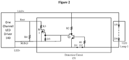
- the current setting resistance Rset has the role of setting the maximum current output of the one channel LED driver 140.
- the maximum current output value may be set in accordance with a standard set by a standards body.
- the current setting resistance Rset can be set either proportionally or inversely proportionally to the maximum current output value.
- the current setting resistance Rset is set proportional to a current output value.
- current setting resistance Rset is proportional to the current output value, the total resistance is decreased in response to the detected absence of an LED lamp, which in turn sets effective output current of an LED driver smaller.
- inventions of Figures 1-3 could be modified to increase total resistance by switching out resistive elements or circuits in parallel with the remaining resistance.
- inverters can be added between MOSFETs and Q gates, and the configuration of resistors is changed. This modified embodiment is explained further below.
- Rset may be matched with a maximum current output value and the entirety of a resistive circuit as the default for when all LED lamps are present.
- a portion of the resistance circuit may be disconnected (rather than connected) in order to maintain the maximum current.
- the added circuit automatically adjusts current to match the number of present LED lamps.
- the added circuit actually includes two identical circuits or sub-circuits, or the same number of identical circuits or sub-circuits as would match the maximum number of possible present LED lamps.
- the embodiment of Figure 1 can be modified to increase total resistance by switching out (rather than switching in) resistive elements or circuits in parallel with the remaining resistance.
- Inverted control signals for the MOSFETs M1 and M2 are produced by adding a first inverter stage between Q1 and the gate of M1, and a second inverter stage between Q2 and the gate of M2.
- a first LED lamp detection circuit 151 for LED Lamp1 in Figure 1 is made up of D1, D2, R1, Q1 and R2.
- NPN transistor Q1 When LED Lamp1 is present, NPN transistor Q1 will be turned on by the voltage drop on D1 and D2 since current flows through LED Lamp1.
- LED- and SGND usually have the same or a very close potential.
- the gate voltage of M1 is low, and metal-oxide semiconductor field-effect transistor (MOSFET) M1 is off.
- MOSFET metal-oxide semiconductor field-effect transistor
- circuit(s) 151, 152 added between the LED driver and LED lamps LED Lamp1 and LED Lamp2, are used to vary the resistance based on the detected number of LED lamps among LED Lamp1 and LED Lamp2.
- additional circuits or sub-circuits may be added to correspond to more potential LED lamps in Figure 1 .
- variable resistance is implemented automatically. That is, based on the presence or absence of an LED lamp, the resistance to set current from the LED driver can be increased or decreased so that the effective current for the present LED lamps is appropriate based, for example, on requirements for standards set to ensure LED lamps do not overheat.
- Presence of LED Lamp2 is sensed by Q2 being on, and M2 will therefore be off. However, when LED LAMP2 is absent or off, Q2 will be off, and the gate voltage on MOSFET M2 will be high so that R7 is in parallel with R4. The total resistance of R7 and R4 are smaller, and this sets effective output current of the LED driver 140 smaller to match the remaining LED lamp.
- variable resistance circuits are implemented using transistors Q1 and Q2, and MOSFETS M1 and M2.
- the variable resistance is provided by adding in resistors R3 and/or R7 in parallel to R4.
- resistors R3 and/or R7 in parallel to R4.
- a single LED driver 140 is shown.
- the LED driver 140 is a single channel LED driver that drives multiple different LEDs or lamps with multiple LEDs.
- the overall LED apparatus shown in Figure 1 may be a retrofit system imposed on a fluorescent lighting system.
- LED Lamp1 and LED Lamp2 may also include features shown in other Figures such as Figures 1a and 1b , with extra terminals intended for support, but shorted so as to be used as switches to switch off power when any expected LED lamp is absent.
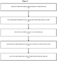
- Figure 4 shows an exemplary method for operation of an exemplary circuit arrangement for the LED lamp(s) with single channel driver, according to an aspect of the present disclosure.
- a light emitting diode apparatus is initially installed with multiple LED lamps at S410.
- the light emitting diode apparatus may be configured with, for example, four LED lamps, and installed as a retrofit assembly at S410.
- the resistance adjusted at S440 may be adjusted higher or lower depending on whether the total resistance is maintained proportional or inversely proportional to current.
- the resistance may be changed by switching in additional resistive elements or a resistive circuit in parallel.
- a default resistive circuit for when all LED lamps are present may including switchable (variable) resistive elements or sub-circuits that can be switched out (rather than in) when an LED lamp is detected to be missing.
- a microprocessor as described herein is tangible and non-transitory. As used herein, the term “non-transitory” is to be interpreted not as an eternal characteristic of a state, but as a characteristic of a state that will last for a period of time. The term “non-transitory” specifically disavows fleeting characteristics such as characteristics of a particular carrier wave or signal or other forms that exist only transitorily in any place at any time.
- a microprocessor is an article of manufacture and/or a machine component.
- a microprocessor for an electronic device is configured to execute software instructions in order to perform functions as described in the various embodiments herein.
- a microprocessor for an electronic device may be a general purpose microprocessor or may be part of an application specific integrated circuit (ASIC). Additionally, any microprocessor described herein may include multiple microprocessors, parallel microprocessors, or both. Multiple microprocessors may be included in, or coupled to, a single device or multiple devices.
- resistive sub-circuit can be controlled logically using a switch and a microprocessor, so that resistance can be varied when LED lamps are absent.
- a light emitting diode (LED) apparatus is configured for driving light emitting diode lamps in parallel.
- the apparatus includes at least one driver circuit that provides a current for the light emitting diode lamps.
- the driver circuit includes a resistor for setting a maximum value of the current.
- the apparatus also includes a circuit that detects presence or absence of each of the light emitting diode lamps. The circuit is configured to adjust the resistor based on the detection of presence or absence.
- the apparatus also includes a single light emitting diode driver, and the apparatus is a retrofit system with the light emitting diodes and the single light emitting diode driver.
- each present light emitting diode lamp comprises a tubular shape.
- the driver adjusts light emitting diode driver current to match an LED lamp current rating using a current setting resistance circuit that includes multiple resistors and transistors.
- the current setting resistance circuit is externally installed on the light emitting diode apparatus.
- a method for driving multiple light emitting diode lamps of a light emitting diode apparatus includes providing a current for the light emitting diode lamps by a driver circuit comprising a resistor used to set a maximum value of the current.
- the method includes detecting presence or absence of each of the plurality of light emitting diode lamps using a detection circuit.
- the method also includes adjusting the resistor based on detecting the presence or absence.
- the resistor is adjusted by switching in parallel resistance in response to detecting the absence of one of the light emitting diode lamps.
- the method further includes adjusting a light emitting diode driver current to match a light emitting diode current rating using the resistor and additional resistors of a current setting resistance circuit comprising multiple resistors and multiple transistors.
- the method includes switching in one identical set of circuit components for each absent light emitting diode lamp.
- the method includes switching out one identical set of circuit components for each absent light emitting diode lamp.
- the teachings of the present disclosure can be used to sense and turn off or adjust the current to the remaining light emitting diode lamps.
- the adjustments can be made using a resistive circuit that can be switched in and out based on the sensing of presence of remaining light emitting diode lamps. As a result, temperatures can be prevented from rising to levels outside of safety standards, and the life of the light emitting diode lamps can be extended.
Landscapes
- Engineering & Computer Science (AREA)
- Physics & Mathematics (AREA)
- Microelectronics & Electronic Packaging (AREA)
- Optics & Photonics (AREA)
- General Engineering & Computer Science (AREA)
- Circuit Arrangement For Electric Light Sources In General (AREA)
- Led Devices (AREA)
Claims (15)
- Leuchtdioden-, LED-, Vorrichtung, die so konfiguriert ist, dass sie mehrere parallel geschaltete LED-Lampen (Lampe 1, Lampe 2) ansteuert, dadurch gekennzeichnet, dass diese umfasst:mindestens eine LED-Treiberschaltung (140), die so eingerichtet ist, dass sie einen LED-Ansteuerstrom für die mehreren LED-Lampen (Lampe 1, Lampe 2) bereitstellt, wobei die LED-Treiberschaltung (140) eine Stromeinstellungs-Widerstandsschaltung zum Einstellen eines Maximalwertes des LED-Ansteuerstroms umfasst; sowieeine Detektionsschaltung (151, 152), die so eingerichtet ist, dass sie das Vorhandensein oder Nichtvorhandensein von jeder der mehreren LED-Lampen (Lampe 1, Lampe 2) durch Messung eines jeweiligen, durch jede der LED-Lampen (Lampe 1, Lampe 2) fließenden LED-Stroms detektiert,wobei die Detektionsschaltung (151, 152) so konfiguriert ist, dass sie die Stromeinstellungs-Widerstandsschaltung aufgrund der Detektion des Vorhandenseins oder Nichtvorhandenseins anpasst.
- Leuchtdiodenvorrichtung nach Anspruch 1, umfassend:eine einzelne LED-Treiberschaltung (140),wobei die LED-Vorrichtung ein Nachrüstsystem ist, das die mehreren LED-Lampen (Lampe 1, Lampe 2) sowie die einzelne LED-Treiberschaltung (140) umfasst.
- Leuchtdiodenvorrichtung nach Anspruch 1,
wobei jede vorhandene LED-Lampe eine röhrenartige Form aufweist. - Leuchtdiodenvorrichtung nach Anspruch 1,
wobei die Stromeinstellungs-Widerstandsschaltung mehrere Einstellwiderstände sowie mehrere Transistoren umfasst. - Leuchtdiodenvorrichtung nach Anspruch 4,
wobei die Stromeinstellungs-Widerstandsschaltung als eine Komponente der Leuchtdiodenvorrichtung installiert ist. - Leuchtdiodenvorrichtung nach Anspruch 4,
wobei die Stromeinstellungs-Widerstandsschaltung identische Schaltungskomponenten in einer identischen Anordnung für jede LED Lampe (Lampe 1, Lampe 2) enthält. - Leuchtdiodenvorrichtung nach Anspruch 1,
wobei die Stromeinstellungs-Widerstandsschaltung so eingerichtet ist, dass sie den LED-Ansteuerstrom der LED-Treiberschaltung (140) aufgrund der Detektion des Vorhandenseins einstellt. - Verfahren zur Ansteuerung mehrerer LED-Lampen (Lampe 1, Lampe 2) einer Leuchtdiodenvorrichtung - wobei die LED-Lampen (Lampe 1, Lampe 2) parallelgeschaltet werden - welches die folgenden Schritte umfasst, wonach:ein LED-Ansteuerstrom für die mehreren LED-Lampen (Lampe 1, Lampe 2) durch eine LED-Treiberschaltung (140) bereitgestellt wird, die eine zum Einstellen eines Maximalwertes des LED-Ansteuerstroms verwendete Stromeinstellungs-Widerstandsschaltung umfasst;das Vorhandensein oder Nichtvorhandensein von jeder der mehreren LED-Lampen (Lampe 1, Lampe 2) unter Verwendung einer Detektionsschaltung (151, 152) detektiert wird, die einen jeweiligen, durch jede LED-Lampe (Lampe 1, Lampe 2) fließenden Strom detektiert, unddie Stromeinstellungs-Widerstandsschaltung aufgrund der Detektion des Vorhandenseins oder Nichtvorhandenseins angepasst wird.
- Verfahren zur Ansteuerung der mehreren LED-Lampen (Lampe 1, Lampe 2) nach Anspruch 8, wobei sich die LED-Lampen (Lampe 1, Lampe 2) in einem Nachrüstsystem mit einer einzelnen LED-Treiberschaltung (140) befinden.
- Verfahren zur Ansteuerung der mehreren LED-Lampen (Lampe 1, Lampe 2) nach Anspruch 8, wobei die Stromeinstellungs-Widerstandsschaltung durch Parallelschalten von Einstellwiderständen in Reaktion auf das Detektieren des Nichtvorhandenseins von einer der Leuchtdiodenlampen (Lampe 1, Lampe 2) angepasst wird.
- Verfahren zur Ansteuerung der mehreren LED-Lampen (Lampe 1, Lampe 2) nach Anspruch 8, das weiterhin beinhaltet, dass:
der LED-Ansteuerstrom unter Verwendung der Stromeinstellungs-Widerstandsschaltung angepasst wird, wobei die Stromeinstellungs-Widerstandsschaltung mehrere Widerstände sowie mehrere Transistoren umfasst. - Verfahren zur Ansteuerung der mehreren LED-Lampen nach Anspruch 11,
wobei die Stromeinstellungs-Widerstandsschaltung eine Komponente der Leuchtdiodenvorrichtung ist. - Verfahren zur Ansteuerung der mehreren LED-Lampen (Lampe 1, Lampe 2) nach Anspruch 11, wobei die Stromeinstellungs-Widerstandsschaltung identische Schaltungskomponenten in einer identischen Anordnung für jede LED Lampe (Lampe 1, Lampe 2) enthält.
- Verfahren zur Ansteuerung der mehreren LED-Lampen (Lampe 1, Lampe 2) nach Anspruch 13, das weiterhin beinhaltet, dass:
in einem identischen Satz Schaltungskomponenten für jede nicht vorhandene LED-Lampe (Lampe 1, Lampe 2) geschaltet wird. - Verfahren zur Ansteuerung der mehreren LED-Lampen (Lampe 1, Lampe 2) nach Anspruch 13, das weiterhin das Abschalten eines identischen Satzes Schaltungskomponenten für jede nicht vorhandene LED-Lampe (Lampe 1, Lampe 2) beinhaltet.
Applications Claiming Priority (3)
| Application Number | Priority Date | Filing Date | Title |
|---|---|---|---|
| US201662368515P | 2016-07-29 | 2016-07-29 | |
| EP16185244 | 2016-08-23 | ||
| PCT/EP2017/067587 WO2018019596A1 (en) | 2016-07-29 | 2017-07-12 | Led lamp(s) with single channel driver |
Publications (2)
| Publication Number | Publication Date |
|---|---|
| EP3491890A1 EP3491890A1 (de) | 2019-06-05 |
| EP3491890B1 true EP3491890B1 (de) | 2021-01-13 |
Family
ID=59383548
Family Applications (1)
| Application Number | Title | Priority Date | Filing Date |
|---|---|---|---|
| EP17742407.4A Active EP3491890B1 (de) | 2016-07-29 | 2017-07-12 | Led-lampe(en) mit einkanaligem treiber |
Country Status (5)
| Country | Link |
|---|---|
| US (1) | US10542591B2 (de) |
| EP (1) | EP3491890B1 (de) |
| JP (1) | JP7126490B2 (de) |
| CN (1) | CN109565915B (de) |
| ES (1) | ES2857820T3 (de) |
Family Cites Families (16)
| Publication number | Priority date | Publication date | Assignee | Title |
|---|---|---|---|---|
| JP2004521467A (ja) | 2001-03-29 | 2004-07-15 | コーニンクレッカ フィリップス エレクトロニクス エヌ ヴィ | 回路装置 |
| TWI479466B (zh) | 2005-05-25 | 2015-04-01 | Koninkl Philips Electronics Nv | 通量補償發光二極體驅動系統及方法 |
| WO2008147903A1 (en) | 2007-05-22 | 2008-12-04 | Marvell World Trade Ltd. | Control of delivery of current through one or more discharge lamps |
| JP4577525B2 (ja) | 2007-05-31 | 2010-11-10 | 東芝ライテック株式会社 | 照明装置 |
| AT507185B1 (de) | 2008-08-07 | 2010-06-15 | Zizala Lichtsysteme Gmbh | Funktionsüberwachung einer led-anordnung |
| JP2010113924A (ja) * | 2008-11-06 | 2010-05-20 | Shindengen Electric Mfg Co Ltd | Led点灯駆動回路、半導体集積回路、および照明器具 |
| DE102008037551B4 (de) | 2008-11-14 | 2013-04-18 | Lear Corporation Gmbh | Vorrichtung zum Betreiben von Leuchtdiodenketten |
| JP5881155B2 (ja) * | 2009-02-12 | 2016-03-09 | コーニンクレッカ フィリップス エヌ ヴェKoninklijke Philips N.V. | 発光デバイスシステム及びドライバ |
| CN102192487B (zh) | 2010-02-28 | 2015-01-14 | 松下电器产业株式会社 | 光源模块和点亮设备以及使用它们的照明设备 |
| JP5406764B2 (ja) * | 2010-03-17 | 2014-02-05 | パナソニック株式会社 | 光源モジュール、およびその点灯装置、ならびにそれらを用いた照明器具 |
| US8845127B2 (en) | 2010-07-05 | 2014-09-30 | Koninklijke Philips N.V. | LED lamp |
| JP5641400B2 (ja) * | 2010-07-26 | 2014-12-17 | 東芝ライテック株式会社 | Ledランプ用電源装置およびledランプシステム |
| WO2012052875A2 (en) | 2010-10-19 | 2012-04-26 | Koninklijke Philips Electronics N.V. | Led retrofit lamp |
| US9163818B2 (en) | 2012-06-15 | 2015-10-20 | Lightel Technologies, Inc. | Linear solid-state lighting with degenerate voltage sensing free of fire and shock hazards |
| DE102012224348A1 (de) | 2012-06-25 | 2014-01-02 | Osram Gmbh | Beleuchtungsanlage mit einer Schnittstelle aufweisend ein Netzgerät und mindestens ein Lichtquellenmodul |
| EP2814302A1 (de) * | 2013-06-10 | 2014-12-17 | OSRAM GmbH | Beleuchtungsmodul und entsprechendes Beleuchtungssystem |
-
2017
- 2017-07-12 CN CN201780046935.5A patent/CN109565915B/zh active Active
- 2017-07-12 ES ES17742407T patent/ES2857820T3/es active Active
- 2017-07-12 JP JP2019504087A patent/JP7126490B2/ja active Active
- 2017-07-12 EP EP17742407.4A patent/EP3491890B1/de active Active
- 2017-07-12 US US16/321,465 patent/US10542591B2/en active Active
Non-Patent Citations (1)
| Title |
|---|
| None * |
Also Published As
| Publication number | Publication date |
|---|---|
| ES2857820T3 (es) | 2021-09-29 |
| US20190166662A1 (en) | 2019-05-30 |
| JP7126490B2 (ja) | 2022-08-26 |
| JP2019523534A (ja) | 2019-08-22 |
| CN109565915B (zh) | 2021-09-14 |
| EP3491890A1 (de) | 2019-06-05 |
| US10542591B2 (en) | 2020-01-21 |
| CN109565915A (zh) | 2019-04-02 |
Similar Documents
| Publication | Publication Date | Title |
|---|---|---|
| US9854631B2 (en) | LED illumination device | |
| US11877362B2 (en) | Light emitting diode thermal foldback control device and method | |
| US10306725B2 (en) | Light source drive device and vehicle lamp | |
| US20150091470A1 (en) | Systems and methods for dimming control with capacitive loads | |
| US20130320857A1 (en) | Light emitting diode driving circuit | |
| US20160178173A1 (en) | Circuit Boards for LED-Based Light Fixtures | |
| JP2015057867A (ja) | ブリーダ回路 | |
| EP2501205B1 (de) | Beleuchtungsvorrichtung | |
| WO2013136241A1 (en) | Shunt device in lighting control system without neutral wire | |
| US20110175550A1 (en) | Apparatus for driving load | |
| US11051378B2 (en) | Eliminating flicker and open load protection for driver compatible with NAFTA dim ECG | |
| TWI584693B (zh) | Dimming device | |
| US20110210679A1 (en) | Device and method for activating LED strings | |
| JP2012160392A (ja) | 点灯制御装置 | |
| EP3491890B1 (de) | Led-lampe(en) mit einkanaligem treiber | |
| US9232597B2 (en) | Lighting device and lighting system with the same | |
| WO2018019596A1 (en) | Led lamp(s) with single channel driver | |
| JP2016149261A (ja) | 光源ユニットおよびそれを用いた照明器具 | |
| US20120074865A1 (en) | Light emitting diode driving device | |
| EP3086377A1 (de) | Led-treiberschaltung und verfahren zur steuerung der led-treiberschaltung | |
| WO2018209273A1 (en) | Active preload for triac dimmers | |
| EP3089556A1 (de) | Beleuchtungslampe, beleuchtungsvorrichtung und beleuchtungssteuerungsschaltung | |
| CN102076158B (zh) | 用于向至少一个光源供电的电路及其控制方法 | |
| WO2020262447A1 (ja) | 車両用灯具システムおよび点灯回路 | |
| KR102274124B1 (ko) | Ac 직결 방식에서의 이중 전원 구동 회로 |
Legal Events
| Date | Code | Title | Description |
|---|---|---|---|
| STAA | Information on the status of an ep patent application or granted ep patent |
Free format text: STATUS: UNKNOWN |
|
| STAA | Information on the status of an ep patent application or granted ep patent |
Free format text: STATUS: THE INTERNATIONAL PUBLICATION HAS BEEN MADE |
|
| PUAI | Public reference made under article 153(3) epc to a published international application that has entered the european phase |
Free format text: ORIGINAL CODE: 0009012 |
|
| STAA | Information on the status of an ep patent application or granted ep patent |
Free format text: STATUS: REQUEST FOR EXAMINATION WAS MADE |
|
| 17P | Request for examination filed |
Effective date: 20190228 |
|
| AK | Designated contracting states |
Kind code of ref document: A1 Designated state(s): AL AT BE BG CH CY CZ DE DK EE ES FI FR GB GR HR HU IE IS IT LI LT LU LV MC MK MT NL NO PL PT RO RS SE SI SK SM TR |
|
| AX | Request for extension of the european patent |
Extension state: BA ME |
|
| STAA | Information on the status of an ep patent application or granted ep patent |
Free format text: STATUS: EXAMINATION IS IN PROGRESS |
|
| 17Q | First examination report despatched |
Effective date: 20190726 |
|
| DAV | Request for validation of the european patent (deleted) | ||
| DAX | Request for extension of the european patent (deleted) | ||
| REG | Reference to a national code |
Ref country code: DE Ref legal event code: R079 Ref document number: 602017031377 Country of ref document: DE Free format text: PREVIOUS MAIN CLASS: H05B0033080000 Ipc: H05B0045370000 |
|
| GRAP | Despatch of communication of intention to grant a patent |
Free format text: ORIGINAL CODE: EPIDOSNIGR1 |
|
| STAA | Information on the status of an ep patent application or granted ep patent |
Free format text: STATUS: GRANT OF PATENT IS INTENDED |
|
| RIC1 | Information provided on ipc code assigned before grant |
Ipc: H05B 45/50 20200101ALI20200723BHEP Ipc: H05B 45/37 20200101AFI20200723BHEP Ipc: F21K 9/27 20160101ALI20200723BHEP |
|
| INTG | Intention to grant announced |
Effective date: 20200805 |
|
| GRAS | Grant fee paid |
Free format text: ORIGINAL CODE: EPIDOSNIGR3 |
|
| GRAA | (expected) grant |
Free format text: ORIGINAL CODE: 0009210 |
|
| STAA | Information on the status of an ep patent application or granted ep patent |
Free format text: STATUS: THE PATENT HAS BEEN GRANTED |
|
| AK | Designated contracting states |
Kind code of ref document: B1 Designated state(s): AL AT BE BG CH CY CZ DE DK EE ES FI FR GB GR HR HU IE IS IT LI LT LU LV MC MK MT NL NO PL PT RO RS SE SI SK SM TR |
|
| REG | Reference to a national code |
Ref country code: GB Ref legal event code: FG4D |
|
| REG | Reference to a national code |
Ref country code: CH Ref legal event code: EP |
|
| REG | Reference to a national code |
Ref country code: IE Ref legal event code: FG4D |
|
| REG | Reference to a national code |
Ref country code: DE Ref legal event code: R096 Ref document number: 602017031377 Country of ref document: DE |
|
| REG | Reference to a national code |
Ref country code: AT Ref legal event code: REF Ref document number: 1355509 Country of ref document: AT Kind code of ref document: T Effective date: 20210215 |
|
| REG | Reference to a national code |
Ref country code: NL Ref legal event code: FP |
|
| REG | Reference to a national code |
Ref country code: SE Ref legal event code: TRGR |
|
| REG | Reference to a national code |
Ref country code: AT Ref legal event code: MK05 Ref document number: 1355509 Country of ref document: AT Kind code of ref document: T Effective date: 20210113 |
|
| REG | Reference to a national code |
Ref country code: LT Ref legal event code: MG9D |
|
| PG25 | Lapsed in a contracting state [announced via postgrant information from national office to epo] |
Ref country code: LT Free format text: LAPSE BECAUSE OF FAILURE TO SUBMIT A TRANSLATION OF THE DESCRIPTION OR TO PAY THE FEE WITHIN THE PRESCRIBED TIME-LIMIT Effective date: 20210113 Ref country code: BG Free format text: LAPSE BECAUSE OF FAILURE TO SUBMIT A TRANSLATION OF THE DESCRIPTION OR TO PAY THE FEE WITHIN THE PRESCRIBED TIME-LIMIT Effective date: 20210413 Ref country code: GR Free format text: LAPSE BECAUSE OF FAILURE TO SUBMIT A TRANSLATION OF THE DESCRIPTION OR TO PAY THE FEE WITHIN THE PRESCRIBED TIME-LIMIT Effective date: 20210414 Ref country code: FI Free format text: LAPSE BECAUSE OF FAILURE TO SUBMIT A TRANSLATION OF THE DESCRIPTION OR TO PAY THE FEE WITHIN THE PRESCRIBED TIME-LIMIT Effective date: 20210113 Ref country code: HR Free format text: LAPSE BECAUSE OF FAILURE TO SUBMIT A TRANSLATION OF THE DESCRIPTION OR TO PAY THE FEE WITHIN THE PRESCRIBED TIME-LIMIT Effective date: 20210113 Ref country code: PT Free format text: LAPSE BECAUSE OF FAILURE TO SUBMIT A TRANSLATION OF THE DESCRIPTION OR TO PAY THE FEE WITHIN THE PRESCRIBED TIME-LIMIT Effective date: 20210513 Ref country code: NO Free format text: LAPSE BECAUSE OF FAILURE TO SUBMIT A TRANSLATION OF THE DESCRIPTION OR TO PAY THE FEE WITHIN THE PRESCRIBED TIME-LIMIT Effective date: 20210413 |
|
| PG25 | Lapsed in a contracting state [announced via postgrant information from national office to epo] |
Ref country code: AT Free format text: LAPSE BECAUSE OF FAILURE TO SUBMIT A TRANSLATION OF THE DESCRIPTION OR TO PAY THE FEE WITHIN THE PRESCRIBED TIME-LIMIT Effective date: 20210113 Ref country code: RS Free format text: LAPSE BECAUSE OF FAILURE TO SUBMIT A TRANSLATION OF THE DESCRIPTION OR TO PAY THE FEE WITHIN THE PRESCRIBED TIME-LIMIT Effective date: 20210113 Ref country code: LV Free format text: LAPSE BECAUSE OF FAILURE TO SUBMIT A TRANSLATION OF THE DESCRIPTION OR TO PAY THE FEE WITHIN THE PRESCRIBED TIME-LIMIT Effective date: 20210113 Ref country code: PL Free format text: LAPSE BECAUSE OF FAILURE TO SUBMIT A TRANSLATION OF THE DESCRIPTION OR TO PAY THE FEE WITHIN THE PRESCRIBED TIME-LIMIT Effective date: 20210113 |
|
| REG | Reference to a national code |
Ref country code: ES Ref legal event code: FG2A Ref document number: 2857820 Country of ref document: ES Kind code of ref document: T3 Effective date: 20210929 |
|
| PG25 | Lapsed in a contracting state [announced via postgrant information from national office to epo] |
Ref country code: IS Free format text: LAPSE BECAUSE OF FAILURE TO SUBMIT A TRANSLATION OF THE DESCRIPTION OR TO PAY THE FEE WITHIN THE PRESCRIBED TIME-LIMIT Effective date: 20210513 |
|
| REG | Reference to a national code |
Ref country code: DE Ref legal event code: R097 Ref document number: 602017031377 Country of ref document: DE |
|
| PG25 | Lapsed in a contracting state [announced via postgrant information from national office to epo] |
Ref country code: EE Free format text: LAPSE BECAUSE OF FAILURE TO SUBMIT A TRANSLATION OF THE DESCRIPTION OR TO PAY THE FEE WITHIN THE PRESCRIBED TIME-LIMIT Effective date: 20210113 Ref country code: CZ Free format text: LAPSE BECAUSE OF FAILURE TO SUBMIT A TRANSLATION OF THE DESCRIPTION OR TO PAY THE FEE WITHIN THE PRESCRIBED TIME-LIMIT Effective date: 20210113 Ref country code: SM Free format text: LAPSE BECAUSE OF FAILURE TO SUBMIT A TRANSLATION OF THE DESCRIPTION OR TO PAY THE FEE WITHIN THE PRESCRIBED TIME-LIMIT Effective date: 20210113 |
|
| PLBE | No opposition filed within time limit |
Free format text: ORIGINAL CODE: 0009261 |
|
| STAA | Information on the status of an ep patent application or granted ep patent |
Free format text: STATUS: NO OPPOSITION FILED WITHIN TIME LIMIT |
|
| PG25 | Lapsed in a contracting state [announced via postgrant information from national office to epo] |
Ref country code: RO Free format text: LAPSE BECAUSE OF FAILURE TO SUBMIT A TRANSLATION OF THE DESCRIPTION OR TO PAY THE FEE WITHIN THE PRESCRIBED TIME-LIMIT Effective date: 20210113 Ref country code: DK Free format text: LAPSE BECAUSE OF FAILURE TO SUBMIT A TRANSLATION OF THE DESCRIPTION OR TO PAY THE FEE WITHIN THE PRESCRIBED TIME-LIMIT Effective date: 20210113 Ref country code: SK Free format text: LAPSE BECAUSE OF FAILURE TO SUBMIT A TRANSLATION OF THE DESCRIPTION OR TO PAY THE FEE WITHIN THE PRESCRIBED TIME-LIMIT Effective date: 20210113 |
|
| 26N | No opposition filed |
Effective date: 20211014 |
|
| PG25 | Lapsed in a contracting state [announced via postgrant information from national office to epo] |
Ref country code: AL Free format text: LAPSE BECAUSE OF FAILURE TO SUBMIT A TRANSLATION OF THE DESCRIPTION OR TO PAY THE FEE WITHIN THE PRESCRIBED TIME-LIMIT Effective date: 20210113 |
|
| PG25 | Lapsed in a contracting state [announced via postgrant information from national office to epo] |
Ref country code: SI Free format text: LAPSE BECAUSE OF FAILURE TO SUBMIT A TRANSLATION OF THE DESCRIPTION OR TO PAY THE FEE WITHIN THE PRESCRIBED TIME-LIMIT Effective date: 20210113 |
|
| REG | Reference to a national code |
Ref country code: CH Ref legal event code: PL |
|
| PG25 | Lapsed in a contracting state [announced via postgrant information from national office to epo] |
Ref country code: MC Free format text: LAPSE BECAUSE OF FAILURE TO SUBMIT A TRANSLATION OF THE DESCRIPTION OR TO PAY THE FEE WITHIN THE PRESCRIBED TIME-LIMIT Effective date: 20210113 |
|
| REG | Reference to a national code |
Ref country code: BE Ref legal event code: MM Effective date: 20210731 |
|
| PG25 | Lapsed in a contracting state [announced via postgrant information from national office to epo] |
Ref country code: LI Free format text: LAPSE BECAUSE OF NON-PAYMENT OF DUE FEES Effective date: 20210731 Ref country code: CH Free format text: LAPSE BECAUSE OF NON-PAYMENT OF DUE FEES Effective date: 20210731 |
|
| PG25 | Lapsed in a contracting state [announced via postgrant information from national office to epo] |
Ref country code: IS Free format text: LAPSE BECAUSE OF FAILURE TO SUBMIT A TRANSLATION OF THE DESCRIPTION OR TO PAY THE FEE WITHIN THE PRESCRIBED TIME-LIMIT Effective date: 20210513 Ref country code: LU Free format text: LAPSE BECAUSE OF NON-PAYMENT OF DUE FEES Effective date: 20210712 |
|
| PG25 | Lapsed in a contracting state [announced via postgrant information from national office to epo] |
Ref country code: IE Free format text: LAPSE BECAUSE OF NON-PAYMENT OF DUE FEES Effective date: 20210712 Ref country code: BE Free format text: LAPSE BECAUSE OF NON-PAYMENT OF DUE FEES Effective date: 20210731 |
|
| P01 | Opt-out of the competence of the unified patent court (upc) registered |
Effective date: 20230425 |
|
| PG25 | Lapsed in a contracting state [announced via postgrant information from national office to epo] |
Ref country code: CY Free format text: LAPSE BECAUSE OF FAILURE TO SUBMIT A TRANSLATION OF THE DESCRIPTION OR TO PAY THE FEE WITHIN THE PRESCRIBED TIME-LIMIT Effective date: 20210113 |
|
| PG25 | Lapsed in a contracting state [announced via postgrant information from national office to epo] |
Ref country code: HU Free format text: LAPSE BECAUSE OF FAILURE TO SUBMIT A TRANSLATION OF THE DESCRIPTION OR TO PAY THE FEE WITHIN THE PRESCRIBED TIME-LIMIT; INVALID AB INITIO Effective date: 20170712 |
|
| PGFP | Annual fee paid to national office [announced via postgrant information from national office to epo] |
Ref country code: NL Payment date: 20230726 Year of fee payment: 7 |
|
| PGFP | Annual fee paid to national office [announced via postgrant information from national office to epo] |
Ref country code: IT Payment date: 20230721 Year of fee payment: 7 Ref country code: GB Payment date: 20230725 Year of fee payment: 7 Ref country code: ES Payment date: 20230816 Year of fee payment: 7 |
|
| PGFP | Annual fee paid to national office [announced via postgrant information from national office to epo] |
Ref country code: SE Payment date: 20230726 Year of fee payment: 7 Ref country code: FR Payment date: 20230725 Year of fee payment: 7 Ref country code: DE Payment date: 20230928 Year of fee payment: 7 |
|
| PG25 | Lapsed in a contracting state [announced via postgrant information from national office to epo] |
Ref country code: MK Free format text: LAPSE BECAUSE OF FAILURE TO SUBMIT A TRANSLATION OF THE DESCRIPTION OR TO PAY THE FEE WITHIN THE PRESCRIBED TIME-LIMIT Effective date: 20210113 |