EP3489996A1 - Mehrlagenkühler - Google Patents
Mehrlagenkühler Download PDFInfo
- Publication number
- EP3489996A1 EP3489996A1 EP18213167.2A EP18213167A EP3489996A1 EP 3489996 A1 EP3489996 A1 EP 3489996A1 EP 18213167 A EP18213167 A EP 18213167A EP 3489996 A1 EP3489996 A1 EP 3489996A1
- Authority
- EP
- European Patent Office
- Prior art keywords
- metallization
- carrier body
- sintered
- uppermost
- ceramic
- Prior art date
- Legal status (The legal status is an assumption and is not a legal conclusion. Google has not performed a legal analysis and makes no representation as to the accuracy of the status listed.)
- Granted
Links
Images
Classifications
-
- H—ELECTRICITY
- H05—ELECTRIC TECHNIQUES NOT OTHERWISE PROVIDED FOR
- H05K—PRINTED CIRCUITS; CASINGS OR CONSTRUCTIONAL DETAILS OF ELECTRIC APPARATUS; MANUFACTURE OF ASSEMBLAGES OF ELECTRICAL COMPONENTS
- H05K1/00—Printed circuits
- H05K1/02—Details
- H05K1/0201—Thermal arrangements, e.g. for cooling, heating or preventing overheating
- H05K1/0203—Cooling of mounted components
-
- H—ELECTRICITY
- H05—ELECTRIC TECHNIQUES NOT OTHERWISE PROVIDED FOR
- H05K—PRINTED CIRCUITS; CASINGS OR CONSTRUCTIONAL DETAILS OF ELECTRIC APPARATUS; MANUFACTURE OF ASSEMBLAGES OF ELECTRICAL COMPONENTS
- H05K1/00—Printed circuits
- H05K1/02—Details
- H05K1/03—Use of materials for the substrate
- H05K1/0306—Inorganic insulating substrates, e.g. ceramic, glass
-
- H—ELECTRICITY
- H05—ELECTRIC TECHNIQUES NOT OTHERWISE PROVIDED FOR
- H05K—PRINTED CIRCUITS; CASINGS OR CONSTRUCTIONAL DETAILS OF ELECTRIC APPARATUS; MANUFACTURE OF ASSEMBLAGES OF ELECTRICAL COMPONENTS
- H05K1/00—Printed circuits
- H05K1/02—Details
- H05K1/09—Use of materials for the conductive, e.g. metallic pattern
-
- H—ELECTRICITY
- H05—ELECTRIC TECHNIQUES NOT OTHERWISE PROVIDED FOR
- H05K—PRINTED CIRCUITS; CASINGS OR CONSTRUCTIONAL DETAILS OF ELECTRIC APPARATUS; MANUFACTURE OF ASSEMBLAGES OF ELECTRICAL COMPONENTS
- H05K1/00—Printed circuits
- H05K1/02—Details
- H05K1/11—Printed elements for providing electric connections to or between printed circuits
- H05K1/111—Pads for surface mounting, e.g. lay-out
-
- H—ELECTRICITY
- H05—ELECTRIC TECHNIQUES NOT OTHERWISE PROVIDED FOR
- H05K—PRINTED CIRCUITS; CASINGS OR CONSTRUCTIONAL DETAILS OF ELECTRIC APPARATUS; MANUFACTURE OF ASSEMBLAGES OF ELECTRICAL COMPONENTS
- H05K1/00—Printed circuits
- H05K1/02—Details
- H05K1/11—Printed elements for providing electric connections to or between printed circuits
- H05K1/115—Via connections; Lands around holes or via connections
-
- H—ELECTRICITY
- H05—ELECTRIC TECHNIQUES NOT OTHERWISE PROVIDED FOR
- H05K—PRINTED CIRCUITS; CASINGS OR CONSTRUCTIONAL DETAILS OF ELECTRIC APPARATUS; MANUFACTURE OF ASSEMBLAGES OF ELECTRICAL COMPONENTS
- H05K1/00—Printed circuits
- H05K1/16—Printed circuits incorporating printed electric components, e.g. printed resistors, capacitors or inductors
- H05K1/165—Printed circuits incorporating printed electric components, e.g. printed resistors, capacitors or inductors incorporating printed inductors
-
- H—ELECTRICITY
- H05—ELECTRIC TECHNIQUES NOT OTHERWISE PROVIDED FOR
- H05K—PRINTED CIRCUITS; CASINGS OR CONSTRUCTIONAL DETAILS OF ELECTRIC APPARATUS; MANUFACTURE OF ASSEMBLAGES OF ELECTRICAL COMPONENTS
- H05K1/00—Printed circuits
- H05K1/16—Printed circuits incorporating printed electric components, e.g. printed resistors, capacitors or inductors
- H05K1/167—Printed circuits incorporating printed electric components, e.g. printed resistors, capacitors or inductors incorporating printed resistors
-
- H—ELECTRICITY
- H05—ELECTRIC TECHNIQUES NOT OTHERWISE PROVIDED FOR
- H05K—PRINTED CIRCUITS; CASINGS OR CONSTRUCTIONAL DETAILS OF ELECTRIC APPARATUS; MANUFACTURE OF ASSEMBLAGES OF ELECTRICAL COMPONENTS
- H05K1/00—Printed circuits
- H05K1/18—Printed circuits structurally associated with non-printed electric components
- H05K1/181—Printed circuits structurally associated with non-printed electric components associated with surface mounted components
-
- H—ELECTRICITY
- H05—ELECTRIC TECHNIQUES NOT OTHERWISE PROVIDED FOR
- H05K—PRINTED CIRCUITS; CASINGS OR CONSTRUCTIONAL DETAILS OF ELECTRIC APPARATUS; MANUFACTURE OF ASSEMBLAGES OF ELECTRICAL COMPONENTS
- H05K3/00—Apparatus or processes for manufacturing printed circuits
- H05K3/0058—Laminating printed circuit boards onto other substrates, e.g. metallic substrates
- H05K3/0067—Laminating printed circuit boards onto other substrates, e.g. metallic substrates onto an inorganic, non-metallic substrate
-
- H—ELECTRICITY
- H05—ELECTRIC TECHNIQUES NOT OTHERWISE PROVIDED FOR
- H05K—PRINTED CIRCUITS; CASINGS OR CONSTRUCTIONAL DETAILS OF ELECTRIC APPARATUS; MANUFACTURE OF ASSEMBLAGES OF ELECTRICAL COMPONENTS
- H05K3/00—Apparatus or processes for manufacturing printed circuits
- H05K3/10—Apparatus or processes for manufacturing printed circuits in which conductive material is applied to the insulating support in such a manner as to form the desired conductive pattern
- H05K3/12—Apparatus or processes for manufacturing printed circuits in which conductive material is applied to the insulating support in such a manner as to form the desired conductive pattern using thick film techniques, e.g. printing techniques to apply the conductive material or similar techniques for applying conductive paste or ink patterns
- H05K3/1216—Apparatus or processes for manufacturing printed circuits in which conductive material is applied to the insulating support in such a manner as to form the desired conductive pattern using thick film techniques, e.g. printing techniques to apply the conductive material or similar techniques for applying conductive paste or ink patterns by screen printing or stencil printing
-
- H—ELECTRICITY
- H05—ELECTRIC TECHNIQUES NOT OTHERWISE PROVIDED FOR
- H05K—PRINTED CIRCUITS; CASINGS OR CONSTRUCTIONAL DETAILS OF ELECTRIC APPARATUS; MANUFACTURE OF ASSEMBLAGES OF ELECTRICAL COMPONENTS
- H05K3/00—Apparatus or processes for manufacturing printed circuits
- H05K3/40—Forming printed elements for providing electric connections to or between printed circuits
- H05K3/4038—Through-connections; Vertical interconnect access [VIA] connections
-
- H—ELECTRICITY
- H05—ELECTRIC TECHNIQUES NOT OTHERWISE PROVIDED FOR
- H05K—PRINTED CIRCUITS; CASINGS OR CONSTRUCTIONAL DETAILS OF ELECTRIC APPARATUS; MANUFACTURE OF ASSEMBLAGES OF ELECTRICAL COMPONENTS
- H05K3/00—Apparatus or processes for manufacturing printed circuits
- H05K3/46—Manufacturing multilayer circuits
- H05K3/4644—Manufacturing multilayer circuits by building the multilayer layer by layer, i.e. build-up multilayer circuits
- H05K3/4673—Application methods or materials of intermediate insulating layers not specially adapted to any one of the previous methods of adding a circuit layer
-
- H—ELECTRICITY
- H10—SEMICONDUCTOR DEVICES; ELECTRIC SOLID-STATE DEVICES NOT OTHERWISE PROVIDED FOR
- H10W—GENERIC PACKAGES, INTERCONNECTIONS, CONNECTORS OR OTHER CONSTRUCTIONAL DETAILS OF DEVICES COVERED BY CLASS H10
- H10W40/00—Arrangements for thermal protection or thermal control
- H10W40/20—Arrangements for cooling
- H10W40/25—Arrangements for cooling characterised by their materials
- H10W40/255—Arrangements for cooling characterised by their materials having a laminate or multilayered structure, e.g. direct bond copper [DBC] ceramic substrates
-
- H—ELECTRICITY
- H10—SEMICONDUCTOR DEVICES; ELECTRIC SOLID-STATE DEVICES NOT OTHERWISE PROVIDED FOR
- H10W—GENERIC PACKAGES, INTERCONNECTIONS, CONNECTORS OR OTHER CONSTRUCTIONAL DETAILS OF DEVICES COVERED BY CLASS H10
- H10W40/00—Arrangements for thermal protection or thermal control
- H10W40/20—Arrangements for cooling
- H10W40/25—Arrangements for cooling characterised by their materials
- H10W40/259—Ceramics or glasses
-
- H—ELECTRICITY
- H10—SEMICONDUCTOR DEVICES; ELECTRIC SOLID-STATE DEVICES NOT OTHERWISE PROVIDED FOR
- H10W—GENERIC PACKAGES, INTERCONNECTIONS, CONNECTORS OR OTHER CONSTRUCTIONAL DETAILS OF DEVICES COVERED BY CLASS H10
- H10W70/00—Package substrates; Interposers; Redistribution layers [RDL]
- H10W70/60—Insulating or insulated package substrates; Interposers; Redistribution layers
- H10W70/67—Insulating or insulated package substrates; Interposers; Redistribution layers characterised by their insulating layers or insulating parts
- H10W70/68—Shapes or dispositions thereof
- H10W70/685—Shapes or dispositions thereof comprising multiple insulating layers
-
- H—ELECTRICITY
- H05—ELECTRIC TECHNIQUES NOT OTHERWISE PROVIDED FOR
- H05K—PRINTED CIRCUITS; CASINGS OR CONSTRUCTIONAL DETAILS OF ELECTRIC APPARATUS; MANUFACTURE OF ASSEMBLAGES OF ELECTRICAL COMPONENTS
- H05K2201/00—Indexing scheme relating to printed circuits covered by H05K1/00
- H05K2201/06—Thermal details
- H05K2201/066—Heatsink mounted on the surface of the printed circuit board [PCB]
-
- H—ELECTRICITY
- H05—ELECTRIC TECHNIQUES NOT OTHERWISE PROVIDED FOR
- H05K—PRINTED CIRCUITS; CASINGS OR CONSTRUCTIONAL DETAILS OF ELECTRIC APPARATUS; MANUFACTURE OF ASSEMBLAGES OF ELECTRICAL COMPONENTS
- H05K3/00—Apparatus or processes for manufacturing printed circuits
- H05K3/10—Apparatus or processes for manufacturing printed circuits in which conductive material is applied to the insulating support in such a manner as to form the desired conductive pattern
- H05K3/12—Apparatus or processes for manufacturing printed circuits in which conductive material is applied to the insulating support in such a manner as to form the desired conductive pattern using thick film techniques, e.g. printing techniques to apply the conductive material or similar techniques for applying conductive paste or ink patterns
- H05K3/1283—After-treatment of the printed patterns, e.g. sintering or curing methods
- H05K3/1291—Firing or sintering at relative high temperatures for patterns on inorganic boards, e.g. co-firing of circuits on green ceramic sheets
Definitions
- Air-cooled or liquid-cooled ceramic carrier bodies made of Al 2 O 3 or AIN have a structured metallization on the surface (Cu or Cu-Ni-Au, or W-Ni-Au) on which directly circuit components can be soldered.
- further circuit elements such as shields, coils, capacitors in the immediate vicinity of the components on the surface of the carrier may be necessary. Due to the meanwhile increased switching frequencies, high-frequency interference radiation is generated, which must be shielded to avoid EMC problems consuming.
- the invention is therefore based on the object, a ceramic carrier body with cooling elements and with sintered Metallmaschines Kunststoffen educate so that more space for other circuit elements (coils, capacitors) is available and / or necessary for shielding the circuits additional circuit elements can be accommodated.
- the ceramic carrier body according to the invention is characterized by cooling elements and sintered metallization regions, which are arranged one above the other in at least two metallization planes, wherein the carrier body has a surface on which sintered metallization regions, which carry and / or are structured in a first metallization plane, are arranged. that they form resistors or coils and these Metallmaschines Hoche are covered together with the components and / or the formed resistors or coils of a ceramic plate and optionally on the ceramic plate more of these sintered metallization in further metallization levels are arranged and are each covered with a ceramic plate and on the top, the cooling elements facing away from the ceramic plate sintered Metallisieruns Symposiume are arranged in a metallization for receiving circuit elements.
- At least one additional metallization plane between circuit plane and cooling plane is thus introduced according to the invention.
- This covered metallization may consist of the same material as the outer circuit plane, or of another, preferably higher melting metal.
- Contact between the metallic elements outside and inside can be made by vias (punched, laser drilled) or by structures pulled out to the edge of the ceramic and connected externally.
- This inner situation can also be structured. It improves the disturbance behavior and can absorb electronic components. By suitable structuring and metal choice, resistors and coils can be realized.
- This inner layer, together with the outer layer can form capacities which are determined by the geometry and the distance.
- the cooling elements are either fins on the carrier body or cooling channels in the interior of the carrier body.
- the additional metallization level (s) carry / carry electronic components and / or are structured such that they form / form resistors or coils.
- the components are incorporated in the metallization in such a way that everything is covered with a ceramic plate can be.
- the metallization (s) is / are patterned to form resistors or coils, the metallization forms a plane on which a ceramic plate can be easily placed.
- the carrier body preferably consists of the ceramic materials aluminum oxide Al 2 O 3 or aluminum nitride ALN. Both materials have good heat conduction and are electrically non-conductive. The Metalliesêts Kunststoffe can easily be sintered with these materials.
- the uppermost metallization level for receiving the circuit elements is preferably made of copper and the inner metallization levels of tungsten.
- VIAS can also be introduced to electrically connect the internal tungsten metallizations to the topmost copper metallization.
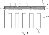
- a ground heat sink 1 with fins 10 (see FIG. 1 ) of AIN with a size of 40 * 40 * 30 mm is coated on the surface with a tungsten glass paste 2 screen-printed in condenser form 15 microns high. With a screen complementary thereto, the remaining area is printed with an insulating paste 3 (contains a glass or the same ceramic from which the heat sink 1 is made). The tungsten glass paste 2 is printed at a location 4 to the outer edge of the heat sink 1.
- the tungsten glass paste 2 and the insulating paste 3 are debindered at 500 ° C.
- a ground ceramic plate 5 of AIN with a dimension of 40 * 40 * 2 mm is placed on the heat sink 1, or on the binder-free tungsten glass paste 2 and the insulating paste 3 and with the printed heat sink 1 at 1300 ° C in moist nitrogen-hydrogen burned on.
- the two ceramic parts, ie the heat sink 1 with its fins 10 and the ceramic plate 5 connect.
- the fired tungsten-glass paste 2 then forms an intermediate layer or a metallization of tungsten. This intermediate layer is also called a metallization region and forms a metallization plane.
- a motif or a metallization is printed with copper paste 6.
- the layer thickness of the copper paste 6 is preferably between 15 and 300 microns.
- the copper print or the copper paste 6 extends to the outer edge 7 of the plate 5 and is connected to the side surface with the tungsten of the intermediate layer by means of a further screen printing step with copper paste 6.
- the copper paste 6 or the copper metallization is baked in nitrogen.
- the invention thus also describes a ceramic carrier body with cooling elements and a circuit plane which consists of sintered metallization regions for receiving circuit elements, wherein at least one additional metallization plane with sintered metallizations is arranged between the circuit plane and the carrier body, each of these additional metallizations being from a ceramic plate is covered and the metallizations of the circuit level are sintered with the uppermost, the cooling elements facing away from the ceramic plate and the sintered metallizations of Metalltechnischesebenen with the metallizations of the circuit level via vias or by pulled out to the edge of the ceramic and externally connected electrically conductive structures is / are connected ,
Landscapes
- Engineering & Computer Science (AREA)
- Microelectronics & Electronic Packaging (AREA)
- Chemical & Material Sciences (AREA)
- Manufacturing & Machinery (AREA)
- Inorganic Chemistry (AREA)
- Ceramic Engineering (AREA)
- Cooling Or The Like Of Semiconductors Or Solid State Devices (AREA)
- Structure Of Printed Boards (AREA)
- Parts Printed On Printed Circuit Boards (AREA)
- Shielding Devices Or Components To Electric Or Magnetic Fields (AREA)
- Cooling Or The Like Of Electrical Apparatus (AREA)
- Manufacturing Of Printed Wiring (AREA)
- Semiconductor Lasers (AREA)
Abstract
Description
- Luft- oder flüssigkeitsgekühlte keramische Trägerkorper aus Al2O3 oder AIN tragen an der Oberflache eine strukturierte Metallisierung (Cu oder Cu-Ni-Au, oder W-Ni-Au) auf die direkt Schaltungsbauteile gelötet werden können. Mit zunehmender Miniaturisierung oder zunehmender Schaltfrequenz bei Leistungsbauteilen können weitere Schaltungselemente wie Abschirmungen, Spulen, Kondensatoren in unmittelbarer Nähe der Bauteile auf der Oberfläche des Trägers notwendig werden. Durch die zwischenzeitlich gestiegenen Schaltfrequenzen wird hochfrequente Störstrahlung erzeugt, welche zur Vermeidung von EMV Problemen aufwändig abgeschirmt werden muss.
- Der Erfindung liegt daher die Aufgabe zugrunde, einen keramischen Trägerkörper mit Kühlelementen und mit versinterten Metallisierungsbereichen so weiterzubilden, dass mehr Platz für weitere Schaltungselemente (Spulen, Kondensatoren) zur Verfügung steht und/oder die zur Abschirmung der Schaltungen notwendigen zusätzlichen Schaltungselemente untergebracht werden können.
- Erfindungsgemäß wird diese Aufgabe durch den im Anspruch 1 beschriebenen Trägerkörper gelöst.
- Der erfindungsgemäße keramische Trägerkörper ist gekennzeichnet durch Kühlelemente und versinterte Metallisierungsbereiche, die in zumindest zwei Metallisierungsebenen übereinander angeordnet sind, wobei der Trägerkörper eine Oberfläche aufweist, auf der in einer ersten Metallisierungsebene versinterte Metallisierungsbereiche angeordnet sind, die elektronische Bauelemente tragen und/oder so strukturiert sind, dass sie Widerstände oder Spulen bilden und diese Metallisierungsbereiche zusammen mit den Bauelementen und/oder den gebildeten Widerständen oder Spulen von einer keramischen Platte abgedeckt sind und optional auf der keramischen Platte weitere von diesen versinterten Metallisierungsbereichen in weiteren Metallisierungsebenen angeordnet sind und jeweils mit einer keramischen Platte agedeckt sind und auf der obersten, den Kühlelementen abgewandten keramischen Platte versinterte Metallisierunsbereiche in einer Metallisierungsebene zur Aufnahme von Schaltungselementen angeordnet sind.
- Um auf dem begrenzten Platz weitere Schaltungselemente (Spulen, Kondensatoren) oder zur Abschirmung der Schaltungen notwendige zusätzliche Schaltungselemente unterbringen zu können, wird somit erfindungsgemäß mindestens eine zusätzliche Metallisierungsebene zwischen Schaltungsebene und Kühlebene (Finnen oder Ebene mit flüssigem Kühlmedium) eingebracht. Diese abgedeckte Metallisierung kann aus dem gleichem Material bestehen, wie die äußere Schaltungsebene, oder auch aus einem anderen, vorzugsweise höher schmelzenden Metall. Ein Kontakt zwischen den metallischen Elementen außen und im Inneren kann durch Vias (gestanzt, lasergebohrt) oder durch bis zum Rand der Keramik herausgezogene und außen verbundene Strukturen hergestellt werden. Diese innere Lage kann zudem strukturiert werden. Sie verbessert das Störverhalten und kann elektronische Bauteile aufnehmen. Durch geeignete Strukturierung und Metallwahl lassen sich Widerstände und Spulen realisieren. Diese innere Lage kann zusammen mit der Deckschicht Kapazitäten ausbilden, die durch die Geometrie und den Abstand bestimmt werden.
- Die Kühlelemente sind entweder Finnen am Trägerkörper oder Kühlkanäle im inneren des Trägerkörpers.
- In bevorzugter erfinderischen Weiterbildung tragen die zusätzliche/n Metallisierungsebene/n elektronische Bauelemente trägt/tragen und/oder sind so strukturiert, dass sie Widerstände oder Spulen bildet/bilden.Die Bauelemente werden dabei so in die Metallisierung eingebaut, dass alles mit einer keramischen Platte abgedeckt werden kann. Wenn die Metallisierung bzw. die Metallisierungsbereiche so strukturiert ist/sind, dass sie Widerstände oder Spulen bildet, bildet die Metallisierung eine Ebene, auf die leicht eine keramische Platte gelegt werden kann.
- Der Trägerkörper besteht bevorzugt aus den keramischen Materialien Aluminiumoxid Al2O3 oder Aluminiumnitrid ALN. Beide Werkstoffe haben eine gute Wärmeleitung und sind elektrisch nicht leitend. Die Metalliesierungsbereiche können mit diesen Materialien leich versintert werden.
- Die oberste Metallisierungsebene zur Aufnahme der Schaltungselemente besteht bevorzugt aus Kupfer und die inneren Metallisierungsebenen aus Wolfram.
- Ein erfindungsgemäßes Verfahren zur Herstellung eines erfindungsgemäßen Trägerkörpers ist dadurch gekennzeichnet, dass zur Herstellung einer Metallisierungsebene nach der Herstellung des keramischen Trägerkörpers mit den Kühlelementen
- a) Teilbereiche der Oberfläche des Trägerkörpers mit einer Wolfram-Glas-Paste im Siebdruck beschichtet werden, wobei an zumindest einer Stelle die Wolfram-Glas-Paste bis an die Außenkante des Trägerkörpers gedruckt wird,
- b) anschließend die nicht beschichteten Flächen mit einer Isolierpaste bedruckt werden, danach die Wolfram-Glas-Paste und die Isolierpaste entbindert werden,
- c) anschließend eine geschliffene keramische Platte auf die entbinderten Pasten gelegt wird
- d) und dann optional die Verfahrensschritte a, b und c wiederholt werden, wobei dann die keramische Platte bedruckt wird und
- e) zum Schluss zur Schaffung von Seiten-Metallisierungenen mit einem weiteren Siebdruckschritt mit Kupferpaste auf die Seitenfläche des Trägerkörpers die inneren Wolfram Metallisierungen mit der obersten Kupfer Metallisierung verbunden werden.
- Die einzelnen Verfahrensschritte sind allgemein bekannt. Anstatt oder zusätzlich zu den Seiten-Metallisierungenen zwischen den Metallisierungsebenen können auch VIAS zur elektrischen Verbindung der inneren Wolfram Metallisierungen mit der obersten Kupfer Metallisierung eingebracht werden.
- Ein geschliffener Kühlkörper 1 mit Finnen 10 (siehe
Figur 1 ) aus AIN mit einer Größe von 40*40*30 mm wird auf der Oberfläche mit einer Wolfram-Glas-Paste 2 im Siebdruck in Kondensatorform 15 µm hoch beschichtet. Mit einem hierzu komplementären Sieb wird mit einer Isolierpaste 3 die restliche Fläche bedruckt (enthält ein Glas oder die gleiche Keramik, aus der auch der Kühlkörper 1 besteht). Die Wolfram-Glas-Paste 2 wird an einer Stelle 4 bis an die Außenkante des Kühlkörpers 1 gedruckt. - Die Wolfram-Glas-Paste 2 und die Isolierpaste 3 werden bei 500°C entbindert. Eine geschliffene keramische Platte 5 aus AIN mit einer Abmessung von 40*40*2 mm wird auf den Kühlkörper 1, bzw. auf die entbinderte Wolfram-Glas-Paste 2 und die Isolierpaste 3 aufgelegt und mit dem bedruckten Kühlkörper 1 bei 1300°C in feuchtem Stickstoff-Wasserstoff aufgebrannt. Dabei verbinden sich die beiden keramischen Teile, d.h. der Kühlkörper 1 mit seinen Finnen 10 und die keramische Platte 5. Die gebrannte Wolfram-Glas-Paste 2 bildet dann eine Zwischenschicht bzw. eine Metallisierung aus Wolfram. Diese Zwischenschicht wird auch als Metallisierungsbereich genannt und bildet eine Metallisierungsebene.
- Auf die Oberseite der Platte 5 aus AIN wird mit Kupferpaste 6 ein Motiv bzw. eine Metallisierung gedruckt. Die Schichtdicke der Kupferpaste 6 liegt vorzugsweise zwischen 15 und 300 µm. Der Kupferdruck bzw. die Kupferpaste 6 reicht bis an die Außenkante 7 der Platte 5 und wird mit einem weiteren Siebdruckschritt mit Kupferpaste 6 auf die Seitenfläche mit dem Wolfram der Zwischenschicht verbunden.
- Bei 910°C wird in Stickstoff die Kupferpaste 6 bzw. die Kupfermetallisierung eingebrannt.
- Die Erfindung beschreibt somit auch einen keramischen Trägerkörper mit Kühlelementen und einer Schaltungsebene, die aus versinterten Metallisierungsbereichen zur Aufnahme von Schaltungselementen besteht, wobei zwischen der Schaltungsebene und dem Trägerkörper zumindest eine zusätzliche Metallisierungsebene mit versinterten Metallisierungen angeordnet ist, wobei jede dieser zusätzlichen Metallisierungen von einer keramischen Platte abgedeckt ist und die Metallisierungen der Schaltungsebene mit der obersten, den Kühlelementen abgewandten keramischen Platte versintert sind und die versinterten Metallisierungen der Metallisierungsebenen mit den Metallisierungen der Schaltungsebene über Vias oder durch bis zum Rand der Keramik herausgezogene und außen verbundene elektrisch leitende Strukturen miteinander verbunden ist/sind.
Claims (14)
- Keramischer Trägerkörper (1) mit Kühlelementen und mit versinterten Metallisierungsbereichen, die in zumindest zwei Metallisierungsebenen übereinander angeordnet sind, wobei der Trägerkörper (1) eine Oberfläche aufweist, auf der in einer ersten Metallisierungsebene versinterte Metallisierungsbereiche angeordnet sind, die so strukturiert sind, dass sie Widerstände oder Spulen bilden und diese Metallisierungsbereiche zusammen mit den gebildeten Widerständen oder Spulen von einer keramischen Platte (5) abgedeckt sind und optional auf der keramischen Platte weitere von diesen versinterten Metallisierungsbereichen in weiteren Metallisierungsebenen angeordnet sind und jeweils mit einer keramischen Platte abgedeckt sind und auf der obersten, den Kühlelementen abgewandten keramischen Platte (5) versinterte Metallisierunsbereiche in einer obersten Metallisierungsebene zur Aufnahme von Schaltungselementen angeordnet sind und die inneren Metallisierungsebenen aus Wolfram bestehen.
- Trägerkörper (1) nach Anspruch 1, dadurch gekennzeichnet, dass die Kühlelemente Finnen (10) am Trägerkörper (1) oder Kühlkanäle im inneren des Trägerkörpers (1) sind.
- Trägerkörper (1) nach Anspruch 1 oder 2, dadurch gekennzeichnet, dass die weitere/n Metallisierungsebene/n so strukturiert ist/sind, dass sie Widerstände oder Spulen bildet/bilden.
- Trägerkörper (1) nach einem der Ansprüche 1 bis 3, dadurch gekennzeichnet, dass der Trägerkörper (1) aus den keramischen Materialien Aluminiumoxid Al2O3 oder Aluminiumnitrid ALN besteht.
- Trägerkörper (1) nach einem der Ansprüche 1 bis 4, dadurch gekennzeichnet, dass die oberste Metallisierungsebene zur Aufnahme der Schaltungselemente aus Kupfer besteht.
- Trägerkörper (1) (1) nach Anspruch 5, dadurch gekennzeichnet, dass zwischen den Metallisierungsebenen VIAS zur elektrischen Verbindung der inneren Wolfram Metallisierungsebenen mit der obersten Kupfer Metallisierungsebene eingebracht sind.
- Trägerkörper (1) nach Anspruch 5 oder 6, dadurch gekennzeichnet, dass auf der Seitenfläche des Trägerkörpers Seiten-Metallisierungen aus Kupfer angeordnet sind, welche die inneren Wolfram Metallisierungsebenen mit der obersten Kupfer Metallisierungsebene verbinden.
- Keramischer Trägerkörper (1) mit Kühlelementen, einer inneren Metallisierungsebene mit versinterten Metallisierungsbereichen auf dem Kühlelement, wobei die innere Metallisierungsebene so strukturiert ist, dass sie Widerstände oder Spulen bildet, mit einer obersten Metallisierungsebene mit versinterten Metallisierungsbereichen, einer keramischen Platte (5) zwischen der inneren Metallisierungsebene und der obersten Metallisierungsebene und die innere Metallisierungsebene aus Wolfram besteht.
- Trägerkörper (1) nach Anspruch 8, dadurch gekennzeichnet, dass auf der obersten Metallisierungsebene Schaltungselemente angeordnet sind.
- Trägerkörper (1) nach Anspruch 8 oder 9, dadurch gekennzeichnet, dass die Kühlelemente Finnen (10) am Trägerkörper (1) oder Kühlkanäle im inneren des Trägerkörpers (1) sind.
- Trägerkörper (1) nach einem der Ansprüche 8 bis 10, dadurch gekennzeichnet, dass eine oder mehrere weitere innere Metallisierungsebenen mit versinterten Metallisierungsbereichen und eine oder mehrere weitere keramische Platten (5) vorgesehen sind, wobei die keramischen Platten (5) zwischen den inneren Metallisierungsebenen angeordnet sind.
- Trägerkörper (1) nach Anspruch 11, dadurch gekennzeichnet, dass zumindest eine der weiteren inneren Metallisierungsebenen mit den versinterten Metallisierungsbereichen so strukturiert ist, dass sie Widerstände oder Spulen bildet.
- Trägerkörper (1) nach einem der Ansprüche 8 bis 12, dadurch gekennzeichnet, dass der Trägerkörper (1) aus den keramischen Materialien Aluminiumoxid Al2O3 oder Aluminiumnitrid ALN und die oberste Metallisierungsebene aus Kupfer besteht.
- Trägerkörper (1) nach einem der Ansprüche 8 bis 13, dadurch gekennzeichnet, dass zwischen der/n inneren Wolfram Metallisierungsebene/n VIAS oder auf der Seitenfläche des Trägerkörpers Seiten-Metallisierungen angeordnet sind, welche die innere/n Wolfram Metallisierungsebene/n mit der obersten Metallisierungsebene elektrisch verbinden.
Priority Applications (1)
| Application Number | Priority Date | Filing Date | Title |
|---|---|---|---|
| HRP20221031TT HRP20221031T1 (hr) | 2014-09-09 | 2015-09-09 | Višeslojni hladnjak |
Applications Claiming Priority (3)
| Application Number | Priority Date | Filing Date | Title |
|---|---|---|---|
| DE102014217978 | 2014-09-09 | ||
| PCT/EP2015/070618 WO2016038094A1 (de) | 2014-09-09 | 2015-09-09 | Mehrlagenkühler |
| EP15762975.9A EP3192097B1 (de) | 2014-09-09 | 2015-09-09 | Mehrlagenkühler |
Related Parent Applications (2)
| Application Number | Title | Priority Date | Filing Date |
|---|---|---|---|
| EP15762975.9A Division EP3192097B1 (de) | 2014-09-09 | 2015-09-09 | Mehrlagenkühler |
| EP15762975.9A Division-Into EP3192097B1 (de) | 2014-09-09 | 2015-09-09 | Mehrlagenkühler |
Publications (2)
| Publication Number | Publication Date |
|---|---|
| EP3489996A1 true EP3489996A1 (de) | 2019-05-29 |
| EP3489996B1 EP3489996B1 (de) | 2022-07-13 |
Family
ID=54105786
Family Applications (2)
| Application Number | Title | Priority Date | Filing Date |
|---|---|---|---|
| EP18213167.2A Active EP3489996B1 (de) | 2014-09-09 | 2015-09-09 | Mehrlagenkühler |
| EP15762975.9A Active EP3192097B1 (de) | 2014-09-09 | 2015-09-09 | Mehrlagenkühler |
Family Applications After (1)
| Application Number | Title | Priority Date | Filing Date |
|---|---|---|---|
| EP15762975.9A Active EP3192097B1 (de) | 2014-09-09 | 2015-09-09 | Mehrlagenkühler |
Country Status (10)
| Country | Link |
|---|---|
| US (1) | US10327323B2 (de) |
| EP (2) | EP3489996B1 (de) |
| JP (1) | JP6761800B2 (de) |
| KR (1) | KR102421016B1 (de) |
| CN (1) | CN106663665B (de) |
| DE (1) | DE102015217231A1 (de) |
| HR (1) | HRP20221031T1 (de) |
| HU (1) | HUE059298T2 (de) |
| PL (1) | PL3489996T3 (de) |
| WO (1) | WO2016038094A1 (de) |
Citations (8)
| Publication number | Priority date | Publication date | Assignee | Title |
|---|---|---|---|---|
| JP2000058381A (ja) * | 1998-08-13 | 2000-02-25 | Murata Mfg Co Ltd | コンデンサ内蔵多層基板 |
| DE69517248T2 (de) * | 1994-07-15 | 2000-10-12 | Mitsubishi Materials Corp., Tokio/Tokyo | Keramik-Gehäuse mit hoher Wärmeabstrahlung |
| DE10035170A1 (de) * | 2000-07-19 | 2002-02-07 | Siemens Ag | Keramikkörper mit Temperiervorrichtung, Verfahren zum Herstellen und Verwendung des Keramikkörpers |
| US20020025439A1 (en) * | 1999-01-26 | 2002-02-28 | Murata Manufacturing Co., Ltd. | Dielectric ceramic composition and multi layered ceramic substrate |
| US20020181185A1 (en) * | 2001-04-26 | 2002-12-05 | Masanao Kabumoto | Multi-layer wiring board |
| EP1320286A2 (de) * | 2001-12-13 | 2003-06-18 | Harris Corporation | Elektronischer Modul mit bei niedriger Temperatur gleichzeitig gebranntem keramischem (LTCC) Substrat mit darin eingebetteter kapazitiever Struktur und zugehörige Verfahren |
| US20030218870A1 (en) * | 2002-05-21 | 2003-11-27 | Fisher Phillip S. | Low temperature co-fired ceramic with improved shrinkage control |
| WO2007107601A2 (de) * | 2006-03-23 | 2007-09-27 | Ceramtec Ag | Trägerkörper für bauelemente oder schaltungen |
Family Cites Families (14)
| Publication number | Priority date | Publication date | Assignee | Title |
|---|---|---|---|---|
| JPH05267854A (ja) * | 1992-03-24 | 1993-10-15 | Mitsubishi Materials Corp | セラミック多層配線基板及びその製造方法 |
| JPH06188569A (ja) * | 1992-12-18 | 1994-07-08 | Denki Kagaku Kogyo Kk | 多層配線基板 |
| JP4493140B2 (ja) * | 2000-01-31 | 2010-06-30 | 京セラ株式会社 | 多層回路基板 |
| US6710433B2 (en) * | 2000-11-15 | 2004-03-23 | Skyworks Solutions, Inc. | Leadless chip carrier with embedded inductor |
| JPWO2002043441A1 (ja) * | 2000-11-24 | 2004-04-02 | イビデン株式会社 | セラミックヒータ、および、セラミックヒータの製造方法 |
| DE602005023039D1 (de) * | 2004-10-29 | 2010-09-30 | Murata Manufacturing Co | Mehrschichtiges substrat mit elektronischer komponente des chiptyps und herstellungsverfahren dafür |
| EP1905076B1 (de) * | 2005-07-19 | 2010-12-22 | Siemens Aktiengesellschaft | Anordnung eines elektrischen bauelements und einer zwei-phasen-kühlvorrichtung und verfahren zum herstellen der anordnung |
| DE102006018034A1 (de) * | 2006-04-19 | 2007-10-31 | Robert Bosch Gmbh | Piezoaktor und Verfahren zu dessen Herstellung |
| DE102008001220A1 (de) * | 2007-04-24 | 2008-10-30 | Ceramtec Ag | Bauteil mit einem Keramikkörper, dessen Oberfläche metallisiert ist |
| JP5093840B2 (ja) * | 2007-05-14 | 2012-12-12 | 株式会社住友金属エレクトロデバイス | 発光素子実装用多層配線基板とその製造方法 |
| JP5713578B2 (ja) * | 2010-04-06 | 2015-05-07 | 株式会社アテクト | 基板の製造方法 |
| CN102238848A (zh) * | 2010-04-27 | 2011-11-09 | 富瑞精密组件(昆山)有限公司 | 散热装置及其气流产生器 |
| US8519532B2 (en) * | 2011-09-12 | 2013-08-27 | Infineon Technologies Ag | Semiconductor device including cladded base plate |
| JP2013123014A (ja) * | 2011-12-12 | 2013-06-20 | Toyota Industries Corp | 半導体装置 |
-
2015
- 2015-09-09 KR KR1020177009417A patent/KR102421016B1/ko not_active Expired - Fee Related
- 2015-09-09 HU HUE18213167A patent/HUE059298T2/hu unknown
- 2015-09-09 CN CN201580048095.7A patent/CN106663665B/zh active Active
- 2015-09-09 EP EP18213167.2A patent/EP3489996B1/de active Active
- 2015-09-09 US US15/509,601 patent/US10327323B2/en active Active
- 2015-09-09 HR HRP20221031TT patent/HRP20221031T1/hr unknown
- 2015-09-09 PL PL18213167.2T patent/PL3489996T3/pl unknown
- 2015-09-09 DE DE102015217231.7A patent/DE102015217231A1/de not_active Withdrawn
- 2015-09-09 EP EP15762975.9A patent/EP3192097B1/de active Active
- 2015-09-09 JP JP2017513494A patent/JP6761800B2/ja active Active
- 2015-09-09 WO PCT/EP2015/070618 patent/WO2016038094A1/de not_active Ceased
Patent Citations (8)
| Publication number | Priority date | Publication date | Assignee | Title |
|---|---|---|---|---|
| DE69517248T2 (de) * | 1994-07-15 | 2000-10-12 | Mitsubishi Materials Corp., Tokio/Tokyo | Keramik-Gehäuse mit hoher Wärmeabstrahlung |
| JP2000058381A (ja) * | 1998-08-13 | 2000-02-25 | Murata Mfg Co Ltd | コンデンサ内蔵多層基板 |
| US20020025439A1 (en) * | 1999-01-26 | 2002-02-28 | Murata Manufacturing Co., Ltd. | Dielectric ceramic composition and multi layered ceramic substrate |
| DE10035170A1 (de) * | 2000-07-19 | 2002-02-07 | Siemens Ag | Keramikkörper mit Temperiervorrichtung, Verfahren zum Herstellen und Verwendung des Keramikkörpers |
| US20020181185A1 (en) * | 2001-04-26 | 2002-12-05 | Masanao Kabumoto | Multi-layer wiring board |
| EP1320286A2 (de) * | 2001-12-13 | 2003-06-18 | Harris Corporation | Elektronischer Modul mit bei niedriger Temperatur gleichzeitig gebranntem keramischem (LTCC) Substrat mit darin eingebetteter kapazitiever Struktur und zugehörige Verfahren |
| US20030218870A1 (en) * | 2002-05-21 | 2003-11-27 | Fisher Phillip S. | Low temperature co-fired ceramic with improved shrinkage control |
| WO2007107601A2 (de) * | 2006-03-23 | 2007-09-27 | Ceramtec Ag | Trägerkörper für bauelemente oder schaltungen |
Also Published As
| Publication number | Publication date |
|---|---|
| CN106663665B (zh) | 2019-09-03 |
| EP3489996B1 (de) | 2022-07-13 |
| KR102421016B1 (ko) | 2022-07-13 |
| KR20170051505A (ko) | 2017-05-11 |
| DE102015217231A1 (de) | 2016-03-10 |
| EP3192097A1 (de) | 2017-07-19 |
| WO2016038094A1 (de) | 2016-03-17 |
| JP2017527123A (ja) | 2017-09-14 |
| CN106663665A (zh) | 2017-05-10 |
| EP3192097B1 (de) | 2019-11-06 |
| US20170265294A1 (en) | 2017-09-14 |
| JP6761800B2 (ja) | 2020-09-30 |
| PL3489996T3 (pl) | 2022-09-19 |
| HUE059298T2 (hu) | 2022-11-28 |
| HRP20221031T1 (hr) | 2022-11-11 |
| US10327323B2 (en) | 2019-06-18 |
Similar Documents
| Publication | Publication Date | Title |
|---|---|---|
| KR102052596B1 (ko) | 칩형 코일 부품 및 그 제조방법 | |
| DE102007007113A1 (de) | Vielschicht-Bauelement | |
| DE102005047106B4 (de) | Leistungshalbleitermodul und Verfahren zur Herstellung | |
| DE102008040906A1 (de) | Leiterplatine mit elektronischem Bauelement | |
| EP3625823B1 (de) | Leistungsmodul mit mindestens einem leistungshalbleiter | |
| EP0620702B1 (de) | Kern für elektrische Verbindungssubstrate und elektrische Verbindungssubstrate mit Kern, sowie Verfahren zu deren Herstellung | |
| DE69904750T2 (de) | Elektrisches bauteil und elektrischer schaltungsmodul mit verbundenen erdungsflächen | |
| DE102015226712A1 (de) | Leiterplatte | |
| EP3437112B1 (de) | Kondensatoranordnung | |
| DE102017220417A1 (de) | Elektronisches Modul | |
| WO2012016898A2 (de) | Verfahren zur herstellung einer mehrzahl von elektronischen bauelementen mit elektromagnetischer schirmung und insbesondere mit wärmeabführung und elektronisches bauelement mit elektromagnetischer schirmung und insbesondere mit wärmeabführung | |
| DE102014010373A1 (de) | Elektronisches Modul für ein Kraftfahrzeug | |
| EP2875514B1 (de) | Elektrisches bauelement umfassend ein anschlusselement mit einem kunststoffkörper | |
| WO2010097387A1 (de) | Mehrlagiger schaltungsträger und verfahren zu dessen herstellung | |
| DE102014209690B4 (de) | Kommutierungszelle | |
| DE102007012049B4 (de) | Elektrisches Bauelement | |
| EP3192097B1 (de) | Mehrlagenkühler | |
| DE102006054085A1 (de) | Bauelement-Anordnung | |
| WO2017194408A2 (de) | Vielschichtbauelement und verfahren zur herstellung eines vielschichtbauelements | |
| WO2017041984A1 (de) | Mehrfunktionale hochstromleiterplatte | |
| DE10217214B4 (de) | Kühlanordnung für eine Schaltungsanordnung | |
| DE10302104A1 (de) | Verfahren zum Herstellen von Schaltungsträgern mit intergrierten passiven Bauelementen | |
| DE102020100742B4 (de) | Lichtmodul, Beleuchtungseinrichtung und Kraftfahrzeug | |
| DE102016200276A1 (de) | Leistungselektronische Schaltung mit einem keramischen Kühlkörper | |
| EP1389404B1 (de) | Verfahren zur abschirmung einer auf einer leiterplatte realisierten elektrischen schaltung und eine entsprechende kombination einer leiterplatte mit einer abschirmung |
Legal Events
| Date | Code | Title | Description |
|---|---|---|---|
| REG | Reference to a national code |
Ref country code: HR Ref legal event code: TUEP Ref document number: P20221031T Country of ref document: HR |
|
| PUAI | Public reference made under article 153(3) epc to a published international application that has entered the european phase |
Free format text: ORIGINAL CODE: 0009012 |
|
| STAA | Information on the status of an ep patent application or granted ep patent |
Free format text: STATUS: THE APPLICATION HAS BEEN PUBLISHED |
|
| AC | Divisional application: reference to earlier application |
Ref document number: 3192097 Country of ref document: EP Kind code of ref document: P |
|
| AK | Designated contracting states |
Kind code of ref document: A1 Designated state(s): AL AT BE BG CH CY CZ DE DK EE ES FI FR GB GR HR HU IE IS IT LI LT LU LV MC MK MT NL NO PL PT RO RS SE SI SK SM TR |
|
| STAA | Information on the status of an ep patent application or granted ep patent |
Free format text: STATUS: REQUEST FOR EXAMINATION WAS MADE |
|
| 17P | Request for examination filed |
Effective date: 20191129 |
|
| RBV | Designated contracting states (corrected) |
Designated state(s): AL AT BE BG CH CY CZ DE DK EE ES FI FR GB GR HR HU IE IS IT LI LT LU LV MC MK MT NL NO PL PT RO RS SE SI SK SM TR |
|
| STAA | Information on the status of an ep patent application or granted ep patent |
Free format text: STATUS: EXAMINATION IS IN PROGRESS |
|
| 17Q | First examination report despatched |
Effective date: 20210728 |
|
| GRAP | Despatch of communication of intention to grant a patent |
Free format text: ORIGINAL CODE: EPIDOSNIGR1 |
|
| STAA | Information on the status of an ep patent application or granted ep patent |
Free format text: STATUS: GRANT OF PATENT IS INTENDED |
|
| INTG | Intention to grant announced |
Effective date: 20220426 |
|
| GRAS | Grant fee paid |
Free format text: ORIGINAL CODE: EPIDOSNIGR3 |
|
| GRAA | (expected) grant |
Free format text: ORIGINAL CODE: 0009210 |
|
| STAA | Information on the status of an ep patent application or granted ep patent |
Free format text: STATUS: THE PATENT HAS BEEN GRANTED |
|
| AC | Divisional application: reference to earlier application |
Ref document number: 3192097 Country of ref document: EP Kind code of ref document: P |
|
| AK | Designated contracting states |
Kind code of ref document: B1 Designated state(s): AL AT BE BG CH CY CZ DE DK EE ES FI FR GB GR HR HU IE IS IT LI LT LU LV MC MK MT NL NO PL PT RO RS SE SI SK SM TR |
|
| REG | Reference to a national code |
Ref country code: CH Ref legal event code: EP |
|
| REG | Reference to a national code |
Ref country code: DE Ref legal event code: R096 Ref document number: 502015015959 Country of ref document: DE |
|
| REG | Reference to a national code |
Ref country code: AT Ref legal event code: REF Ref document number: 1504705 Country of ref document: AT Kind code of ref document: T Effective date: 20220815 |
|
| REG | Reference to a national code |
Ref country code: IE Ref legal event code: FG4D Free format text: LANGUAGE OF EP DOCUMENT: GERMAN Ref country code: NL Ref legal event code: FP |
|
| REG | Reference to a national code |
Ref country code: RO Ref legal event code: EPE |
|
| REG | Reference to a national code |
Ref country code: HR Ref legal event code: ODRP Ref document number: P20221031T Country of ref document: HR Payment date: 20220906 Year of fee payment: 8 |
|
| REG | Reference to a national code |
Ref country code: LT Ref legal event code: MG9D |
|
| REG | Reference to a national code |
Ref country code: HR Ref legal event code: T1PR Ref document number: P20221031 Country of ref document: HR |
|
| REG | Reference to a national code |
Ref country code: HU Ref legal event code: AG4A Ref document number: E059298 Country of ref document: HU |
|
| PG25 | Lapsed in a contracting state [announced via postgrant information from national office to epo] |
Ref country code: SE Free format text: LAPSE BECAUSE OF FAILURE TO SUBMIT A TRANSLATION OF THE DESCRIPTION OR TO PAY THE FEE WITHIN THE PRESCRIBED TIME-LIMIT Effective date: 20220713 Ref country code: RS Free format text: LAPSE BECAUSE OF FAILURE TO SUBMIT A TRANSLATION OF THE DESCRIPTION OR TO PAY THE FEE WITHIN THE PRESCRIBED TIME-LIMIT Effective date: 20220713 Ref country code: PT Free format text: LAPSE BECAUSE OF FAILURE TO SUBMIT A TRANSLATION OF THE DESCRIPTION OR TO PAY THE FEE WITHIN THE PRESCRIBED TIME-LIMIT Effective date: 20221114 Ref country code: NO Free format text: LAPSE BECAUSE OF FAILURE TO SUBMIT A TRANSLATION OF THE DESCRIPTION OR TO PAY THE FEE WITHIN THE PRESCRIBED TIME-LIMIT Effective date: 20221013 Ref country code: LV Free format text: LAPSE BECAUSE OF FAILURE TO SUBMIT A TRANSLATION OF THE DESCRIPTION OR TO PAY THE FEE WITHIN THE PRESCRIBED TIME-LIMIT Effective date: 20220713 Ref country code: LT Free format text: LAPSE BECAUSE OF FAILURE TO SUBMIT A TRANSLATION OF THE DESCRIPTION OR TO PAY THE FEE WITHIN THE PRESCRIBED TIME-LIMIT Effective date: 20220713 Ref country code: FI Free format text: LAPSE BECAUSE OF FAILURE TO SUBMIT A TRANSLATION OF THE DESCRIPTION OR TO PAY THE FEE WITHIN THE PRESCRIBED TIME-LIMIT Effective date: 20220713 Ref country code: ES Free format text: LAPSE BECAUSE OF FAILURE TO SUBMIT A TRANSLATION OF THE DESCRIPTION OR TO PAY THE FEE WITHIN THE PRESCRIBED TIME-LIMIT Effective date: 20220713 |
|
| PG25 | Lapsed in a contracting state [announced via postgrant information from national office to epo] |
Ref country code: IS Free format text: LAPSE BECAUSE OF FAILURE TO SUBMIT A TRANSLATION OF THE DESCRIPTION OR TO PAY THE FEE WITHIN THE PRESCRIBED TIME-LIMIT Effective date: 20221113 Ref country code: GR Free format text: LAPSE BECAUSE OF FAILURE TO SUBMIT A TRANSLATION OF THE DESCRIPTION OR TO PAY THE FEE WITHIN THE PRESCRIBED TIME-LIMIT Effective date: 20221014 |
|
| REG | Reference to a national code |
Ref country code: DE Ref legal event code: R097 Ref document number: 502015015959 Country of ref document: DE |
|
| PG25 | Lapsed in a contracting state [announced via postgrant information from national office to epo] |
Ref country code: SM Free format text: LAPSE BECAUSE OF FAILURE TO SUBMIT A TRANSLATION OF THE DESCRIPTION OR TO PAY THE FEE WITHIN THE PRESCRIBED TIME-LIMIT Effective date: 20220713 Ref country code: MC Free format text: LAPSE BECAUSE OF FAILURE TO SUBMIT A TRANSLATION OF THE DESCRIPTION OR TO PAY THE FEE WITHIN THE PRESCRIBED TIME-LIMIT Effective date: 20220713 Ref country code: DK Free format text: LAPSE BECAUSE OF FAILURE TO SUBMIT A TRANSLATION OF THE DESCRIPTION OR TO PAY THE FEE WITHIN THE PRESCRIBED TIME-LIMIT Effective date: 20220713 |
|
| REG | Reference to a national code |
Ref country code: CH Ref legal event code: PL |
|
| PLBE | No opposition filed within time limit |
Free format text: ORIGINAL CODE: 0009261 |
|
| STAA | Information on the status of an ep patent application or granted ep patent |
Free format text: STATUS: NO OPPOSITION FILED WITHIN TIME LIMIT |
|
| REG | Reference to a national code |
Ref country code: BE Ref legal event code: MM Effective date: 20220930 |
|
| PG25 | Lapsed in a contracting state [announced via postgrant information from national office to epo] |
Ref country code: SK Free format text: LAPSE BECAUSE OF FAILURE TO SUBMIT A TRANSLATION OF THE DESCRIPTION OR TO PAY THE FEE WITHIN THE PRESCRIBED TIME-LIMIT Effective date: 20220713 Ref country code: EE Free format text: LAPSE BECAUSE OF FAILURE TO SUBMIT A TRANSLATION OF THE DESCRIPTION OR TO PAY THE FEE WITHIN THE PRESCRIBED TIME-LIMIT Effective date: 20220713 |
|
| 26N | No opposition filed |
Effective date: 20230414 |
|
| P01 | Opt-out of the competence of the unified patent court (upc) registered |
Effective date: 20230516 |
|
| PG25 | Lapsed in a contracting state [announced via postgrant information from national office to epo] |
Ref country code: LU Free format text: LAPSE BECAUSE OF NON-PAYMENT OF DUE FEES Effective date: 20220909 Ref country code: AL Free format text: LAPSE BECAUSE OF FAILURE TO SUBMIT A TRANSLATION OF THE DESCRIPTION OR TO PAY THE FEE WITHIN THE PRESCRIBED TIME-LIMIT Effective date: 20220713 |
|
| PG25 | Lapsed in a contracting state [announced via postgrant information from national office to epo] |
Ref country code: LI Free format text: LAPSE BECAUSE OF NON-PAYMENT OF DUE FEES Effective date: 20220930 Ref country code: IE Free format text: LAPSE BECAUSE OF NON-PAYMENT OF DUE FEES Effective date: 20220909 Ref country code: CH Free format text: LAPSE BECAUSE OF NON-PAYMENT OF DUE FEES Effective date: 20220930 |
|
| PG25 | Lapsed in a contracting state [announced via postgrant information from national office to epo] |
Ref country code: SI Free format text: LAPSE BECAUSE OF FAILURE TO SUBMIT A TRANSLATION OF THE DESCRIPTION OR TO PAY THE FEE WITHIN THE PRESCRIBED TIME-LIMIT Effective date: 20220713 |
|
| REG | Reference to a national code |
Ref country code: HR Ref legal event code: ODRP Ref document number: P20221031 Country of ref document: HR Payment date: 20230901 Year of fee payment: 9 |
|
| PG25 | Lapsed in a contracting state [announced via postgrant information from national office to epo] |
Ref country code: BE Free format text: LAPSE BECAUSE OF NON-PAYMENT OF DUE FEES Effective date: 20220930 |
|
| PG25 | Lapsed in a contracting state [announced via postgrant information from national office to epo] |
Ref country code: CY Free format text: LAPSE BECAUSE OF FAILURE TO SUBMIT A TRANSLATION OF THE DESCRIPTION OR TO PAY THE FEE WITHIN THE PRESCRIBED TIME-LIMIT Effective date: 20220713 |
|
| PG25 | Lapsed in a contracting state [announced via postgrant information from national office to epo] |
Ref country code: MK Free format text: LAPSE BECAUSE OF FAILURE TO SUBMIT A TRANSLATION OF THE DESCRIPTION OR TO PAY THE FEE WITHIN THE PRESCRIBED TIME-LIMIT Effective date: 20220713 |
|
| REG | Reference to a national code |
Ref country code: HR Ref legal event code: ODRP Ref document number: P20221031 Country of ref document: HR Payment date: 20240829 Year of fee payment: 10 |
|
| PG25 | Lapsed in a contracting state [announced via postgrant information from national office to epo] |
Ref country code: MT Free format text: LAPSE BECAUSE OF FAILURE TO SUBMIT A TRANSLATION OF THE DESCRIPTION OR TO PAY THE FEE WITHIN THE PRESCRIBED TIME-LIMIT Effective date: 20220713 |
|
| PGFP | Annual fee paid to national office [announced via postgrant information from national office to epo] |
Ref country code: BG Payment date: 20240924 Year of fee payment: 10 |
|
| PGFP | Annual fee paid to national office [announced via postgrant information from national office to epo] |
Ref country code: HR Payment date: 20240829 Year of fee payment: 10 |
|
| PGFP | Annual fee paid to national office [announced via postgrant information from national office to epo] |
Ref country code: CZ Payment date: 20240903 Year of fee payment: 10 |
|
| PGFP | Annual fee paid to national office [announced via postgrant information from national office to epo] |
Ref country code: AT Payment date: 20240919 Year of fee payment: 10 |
|
| PGFP | Annual fee paid to national office [announced via postgrant information from national office to epo] |
Ref country code: PL Payment date: 20240821 Year of fee payment: 10 |
|
| PGFP | Annual fee paid to national office [announced via postgrant information from national office to epo] |
Ref country code: HU Payment date: 20240920 Year of fee payment: 10 |
|
| PGFP | Annual fee paid to national office [announced via postgrant information from national office to epo] |
Ref country code: RO Payment date: 20240905 Year of fee payment: 10 Ref country code: IT Payment date: 20240924 Year of fee payment: 10 |
|
| PGFP | Annual fee paid to national office [announced via postgrant information from national office to epo] |
Ref country code: TR Payment date: 20240902 Year of fee payment: 10 |
|
| PGFP | Annual fee paid to national office [announced via postgrant information from national office to epo] |
Ref country code: DE Payment date: 20250919 Year of fee payment: 11 |
|
| PGFP | Annual fee paid to national office [announced via postgrant information from national office to epo] |
Ref country code: NL Payment date: 20250918 Year of fee payment: 11 |
|
| PGFP | Annual fee paid to national office [announced via postgrant information from national office to epo] |
Ref country code: GB Payment date: 20250919 Year of fee payment: 11 |
|
| PGFP | Annual fee paid to national office [announced via postgrant information from national office to epo] |
Ref country code: FR Payment date: 20250922 Year of fee payment: 11 |
|
| REG | Reference to a national code |
Ref country code: DE Ref legal event code: R079 Ref document number: 502015015959 Country of ref document: DE Free format text: PREVIOUS MAIN CLASS: H01L0023373000 Ipc: H10W0040250000 |
|
| REG | Reference to a national code |
Ref country code: HR Ref legal event code: PBON Ref document number: P20221031 Country of ref document: HR Effective date: 20250909 |
|
| PG25 | Lapsed in a contracting state [announced via postgrant information from national office to epo] |
Ref country code: HR Free format text: LAPSE BECAUSE OF NON-PAYMENT OF DUE FEES Effective date: 20250909 |
|
| PG25 | Lapsed in a contracting state [announced via postgrant information from national office to epo] |
Ref country code: RO Free format text: LAPSE BECAUSE OF NON-PAYMENT OF DUE FEES Effective date: 20250909 |
|
| PG25 | Lapsed in a contracting state [announced via postgrant information from national office to epo] |
Ref country code: CZ Free format text: LAPSE BECAUSE OF NON-PAYMENT OF DUE FEES Effective date: 20250909 |