EP3489570A1 - Tube-shaped led lighting device - Google Patents
Tube-shaped led lighting device Download PDFInfo
- Publication number
- EP3489570A1 EP3489570A1 EP17831390.4A EP17831390A EP3489570A1 EP 3489570 A1 EP3489570 A1 EP 3489570A1 EP 17831390 A EP17831390 A EP 17831390A EP 3489570 A1 EP3489570 A1 EP 3489570A1
- Authority
- EP
- European Patent Office
- Prior art keywords
- tube
- cover
- led lighting
- lighting device
- shaped led
- Prior art date
- Legal status (The legal status is an assumption and is not a legal conclusion. Google has not performed a legal analysis and makes no representation as to the accuracy of the status listed.)
- Pending
Links
Images







Classifications
-
- F—MECHANICAL ENGINEERING; LIGHTING; HEATING; WEAPONS; BLASTING
- F21—LIGHTING
- F21K—NON-ELECTRIC LIGHT SOURCES USING LUMINESCENCE; LIGHT SOURCES USING ELECTROCHEMILUMINESCENCE; LIGHT SOURCES USING CHARGES OF COMBUSTIBLE MATERIAL; LIGHT SOURCES USING SEMICONDUCTOR DEVICES AS LIGHT-GENERATING ELEMENTS; LIGHT SOURCES NOT OTHERWISE PROVIDED FOR
- F21K9/00—Light sources using semiconductor devices as light-generating elements, e.g. using light-emitting diodes [LED] or lasers
- F21K9/20—Light sources comprising attachment means
- F21K9/27—Retrofit light sources for lighting devices with two fittings for each light source, e.g. for substitution of fluorescent tubes
- F21K9/278—Arrangement or mounting of circuit elements integrated in the light source
-
- F—MECHANICAL ENGINEERING; LIGHTING; HEATING; WEAPONS; BLASTING
- F21—LIGHTING
- F21K—NON-ELECTRIC LIGHT SOURCES USING LUMINESCENCE; LIGHT SOURCES USING ELECTROCHEMILUMINESCENCE; LIGHT SOURCES USING CHARGES OF COMBUSTIBLE MATERIAL; LIGHT SOURCES USING SEMICONDUCTOR DEVICES AS LIGHT-GENERATING ELEMENTS; LIGHT SOURCES NOT OTHERWISE PROVIDED FOR
- F21K9/00—Light sources using semiconductor devices as light-generating elements, e.g. using light-emitting diodes [LED] or lasers
- F21K9/20—Light sources comprising attachment means
- F21K9/27—Retrofit light sources for lighting devices with two fittings for each light source, e.g. for substitution of fluorescent tubes
-
- F—MECHANICAL ENGINEERING; LIGHTING; HEATING; WEAPONS; BLASTING
- F21—LIGHTING
- F21K—NON-ELECTRIC LIGHT SOURCES USING LUMINESCENCE; LIGHT SOURCES USING ELECTROCHEMILUMINESCENCE; LIGHT SOURCES USING CHARGES OF COMBUSTIBLE MATERIAL; LIGHT SOURCES USING SEMICONDUCTOR DEVICES AS LIGHT-GENERATING ELEMENTS; LIGHT SOURCES NOT OTHERWISE PROVIDED FOR
- F21K9/00—Light sources using semiconductor devices as light-generating elements, e.g. using light-emitting diodes [LED] or lasers
- F21K9/20—Light sources comprising attachment means
- F21K9/27—Retrofit light sources for lighting devices with two fittings for each light source, e.g. for substitution of fluorescent tubes
- F21K9/272—Details of end parts, i.e. the parts that connect the light source to a fitting; Arrangement of components within end parts
-
- F—MECHANICAL ENGINEERING; LIGHTING; HEATING; WEAPONS; BLASTING
- F21—LIGHTING
- F21K—NON-ELECTRIC LIGHT SOURCES USING LUMINESCENCE; LIGHT SOURCES USING ELECTROCHEMILUMINESCENCE; LIGHT SOURCES USING CHARGES OF COMBUSTIBLE MATERIAL; LIGHT SOURCES USING SEMICONDUCTOR DEVICES AS LIGHT-GENERATING ELEMENTS; LIGHT SOURCES NOT OTHERWISE PROVIDED FOR
- F21K9/00—Light sources using semiconductor devices as light-generating elements, e.g. using light-emitting diodes [LED] or lasers
- F21K9/60—Optical arrangements integrated in the light source, e.g. for improving the colour rendering index or the light extraction
- F21K9/65—Optical arrangements integrated in the light source, e.g. for improving the colour rendering index or the light extraction specially adapted for changing the characteristics or the distribution of the light, e.g. by adjustment of parts
-
- F—MECHANICAL ENGINEERING; LIGHTING; HEATING; WEAPONS; BLASTING
- F21—LIGHTING
- F21V—FUNCTIONAL FEATURES OR DETAILS OF LIGHTING DEVICES OR SYSTEMS THEREOF; STRUCTURAL COMBINATIONS OF LIGHTING DEVICES WITH OTHER ARTICLES, NOT OTHERWISE PROVIDED FOR
- F21V19/00—Fastening of light sources or lamp holders
- F21V19/001—Fastening of light sources or lamp holders the light sources being semiconductors devices, e.g. LEDs
- F21V19/003—Fastening of light source holders, e.g. of circuit boards or substrates holding light sources
- F21V19/0045—Fastening of light source holders, e.g. of circuit boards or substrates holding light sources by tongue and groove connections, e.g. dovetail interlocking means fixed by sliding
-
- F—MECHANICAL ENGINEERING; LIGHTING; HEATING; WEAPONS; BLASTING
- F21—LIGHTING
- F21V—FUNCTIONAL FEATURES OR DETAILS OF LIGHTING DEVICES OR SYSTEMS THEREOF; STRUCTURAL COMBINATIONS OF LIGHTING DEVICES WITH OTHER ARTICLES, NOT OTHERWISE PROVIDED FOR
- F21V23/00—Arrangement of electric circuit elements in or on lighting devices
- F21V23/02—Arrangement of electric circuit elements in or on lighting devices the elements being transformers, impedances or power supply units, e.g. a transformer with a rectifier
- F21V23/023—Power supplies in a casing
-
- F—MECHANICAL ENGINEERING; LIGHTING; HEATING; WEAPONS; BLASTING
- F21—LIGHTING
- F21V—FUNCTIONAL FEATURES OR DETAILS OF LIGHTING DEVICES OR SYSTEMS THEREOF; STRUCTURAL COMBINATIONS OF LIGHTING DEVICES WITH OTHER ARTICLES, NOT OTHERWISE PROVIDED FOR
- F21V23/00—Arrangement of electric circuit elements in or on lighting devices
- F21V23/06—Arrangement of electric circuit elements in or on lighting devices the elements being coupling devices, e.g. connectors
-
- F—MECHANICAL ENGINEERING; LIGHTING; HEATING; WEAPONS; BLASTING
- F21—LIGHTING
- F21V—FUNCTIONAL FEATURES OR DETAILS OF LIGHTING DEVICES OR SYSTEMS THEREOF; STRUCTURAL COMBINATIONS OF LIGHTING DEVICES WITH OTHER ARTICLES, NOT OTHERWISE PROVIDED FOR
- F21V29/00—Protecting lighting devices from thermal damage; Cooling or heating arrangements specially adapted for lighting devices or systems
- F21V29/50—Cooling arrangements
- F21V29/70—Cooling arrangements characterised by passive heat-dissipating elements, e.g. heat-sinks
- F21V29/74—Cooling arrangements characterised by passive heat-dissipating elements, e.g. heat-sinks with fins or blades
-
- F—MECHANICAL ENGINEERING; LIGHTING; HEATING; WEAPONS; BLASTING
- F21—LIGHTING
- F21V—FUNCTIONAL FEATURES OR DETAILS OF LIGHTING DEVICES OR SYSTEMS THEREOF; STRUCTURAL COMBINATIONS OF LIGHTING DEVICES WITH OTHER ARTICLES, NOT OTHERWISE PROVIDED FOR
- F21V3/00—Globes; Bowls; Cover glasses
- F21V3/04—Globes; Bowls; Cover glasses characterised by materials, surface treatments or coatings
- F21V3/06—Globes; Bowls; Cover glasses characterised by materials, surface treatments or coatings characterised by the material
- F21V3/061—Globes; Bowls; Cover glasses characterised by materials, surface treatments or coatings characterised by the material the material being glass
-
- F—MECHANICAL ENGINEERING; LIGHTING; HEATING; WEAPONS; BLASTING
- F21—LIGHTING
- F21V—FUNCTIONAL FEATURES OR DETAILS OF LIGHTING DEVICES OR SYSTEMS THEREOF; STRUCTURAL COMBINATIONS OF LIGHTING DEVICES WITH OTHER ARTICLES, NOT OTHERWISE PROVIDED FOR
- F21V29/00—Protecting lighting devices from thermal damage; Cooling or heating arrangements specially adapted for lighting devices or systems
- F21V29/50—Cooling arrangements
- F21V29/70—Cooling arrangements characterised by passive heat-dissipating elements, e.g. heat-sinks
- F21V29/74—Cooling arrangements characterised by passive heat-dissipating elements, e.g. heat-sinks with fins or blades
- F21V29/76—Cooling arrangements characterised by passive heat-dissipating elements, e.g. heat-sinks with fins or blades with essentially identical parallel planar fins or blades, e.g. with comb-like cross-section
- F21V29/763—Cooling arrangements characterised by passive heat-dissipating elements, e.g. heat-sinks with fins or blades with essentially identical parallel planar fins or blades, e.g. with comb-like cross-section the planes containing the fins or blades having the direction of the light emitting axis
-
- F—MECHANICAL ENGINEERING; LIGHTING; HEATING; WEAPONS; BLASTING
- F21—LIGHTING
- F21Y—INDEXING SCHEME ASSOCIATED WITH SUBCLASSES F21K, F21L, F21S and F21V, RELATING TO THE FORM OR THE KIND OF THE LIGHT SOURCES OR OF THE COLOUR OF THE LIGHT EMITTED
- F21Y2103/00—Elongate light sources, e.g. fluorescent tubes
- F21Y2103/10—Elongate light sources, e.g. fluorescent tubes comprising a linear array of point-like light-generating elements
-
- F—MECHANICAL ENGINEERING; LIGHTING; HEATING; WEAPONS; BLASTING
- F21—LIGHTING
- F21Y—INDEXING SCHEME ASSOCIATED WITH SUBCLASSES F21K, F21L, F21S and F21V, RELATING TO THE FORM OR THE KIND OF THE LIGHT SOURCES OR OF THE COLOUR OF THE LIGHT EMITTED
- F21Y2115/00—Light-generating elements of semiconductor light sources
- F21Y2115/10—Light-emitting diodes [LED]
Definitions
- Exemplary embodiments of the disclosure relate to a tube-shaped LED lighting device.
- a light emitting diode refers to a semiconductor device configured to emit light upon application of electric current thereto.
- the LED is a solid device with various advantages of environmentally friendliness due to no use of mercury, long lifespan and low power consumption and has attracted attention as a new light source.
- LEDs have a problem of heat generation in operation. Inefficient heat dissipation of the LEDs can cause deterioration in lifespan and intensity of illumination.
- An upper temperature limit for efficient turn-on of the LEDs is about 60°C and it is believed that performance of an LED lighting device is directly related to heat dissipation.
- UV light generally refers to light in the wavelength band of 100 nm to 400 nm and has higher energy than visible light. UV light emitted from the sun is divided into ultraviolet-A, ultraviolet-B, and ultraviolet-C, and it is known in the art that most UV-C is absorbed by the ozone layer and UV-A and UV-B reach the ground.
- a UV lamp includes a lamp tube and a lighting device disposed in the lamp tube and emitting UV light.
- the lamp tube is required to have high transmittance with respect to UV light and not to be deformed when exposed to UV light for a long period of time.
- Exemplary embodiments of the disclosure provide a tube-shaped LED lighting device with improved heat dissipation.
- Exemplary embodiments of the disclosure provide a tube-shaped LED lighting device free from wire bonding to prevent failure due to open circuit and short circuit.
- Exemplary embodiments of the disclosure provide a UV lamp having improved performance and reliability and a method of manufacturing the same.
- a tube-shaped LED lighting device includes: a substrate; a light emitting device mounted on the substrate; a heat sink having one surface on which the substrate is seated, the heat sink including a groove portion formed on opposite side surfaces thereof; a cover receiving the heat sink, the substrate and the light emitting device therein and including an overhang protruding from an inner wall thereof to be inserted into the groove portion; and a base coupled to each of opposite ends of the cover, wherein the opposite side surfaces of the heat sink have a shape corresponding to the inner wall of the cover.
- a tube-shaped LED lighting device includes: a substrate; a light emitting device mounted on the substrate; a heat sink having one surface on which the substrate is seated, the heat sing including a groove portion formed on opposite side surfaces thereof; a cover receiving the heat sink, the substrate and the light emitting device therein, and including an overhang protruding from an inner wall thereof to be inserted into the groove portion; and a base coupled to each of opposite ends of the cover, wherein the substrate has one end placed inside the base after passing through the base.
- a UV lamp includes: a lamp tube including an upper cover and a lower cover integrally formed with the upper cover; a printed circuit board secured inside the lamp tube; and at least one UV light emitting device disposed on the printed circuit board to face the upper cover and operated under control of the printed circuit board, wherein the at least one UV light emitting device emits UV light having a wavelength of 360 nm or more toward the upper cover, the upper cover comprising polymethyl methacrylate.
- the UV lamp may further include a flame retardant layer disposed between the printed circuit board and the upper cover.
- the UV lamp may further include a heat sink secured inside the lamp tube and adapted to dissipate heat generated from the printed circuit board.
- the heat sink may be formed at an upper portion thereof with a groove, the printed circuit board and the flame retardant layer may be placed in the groove, and the flame retardant layer may cover the printed circuit board.
- the UV lamp may further include a heat sink secured inside the lamp tube and adapted to dissipate heat generated from the printed circuit board.
- the heat sink may be formed at an upper side thereof with a groove, the printed circuit board may be placed in the groove, and the flame retardant layer may cover the upper side of the heat sink and the printed circuit board.
- the UV lamp may further include: a heat sink adapted to support the printed circuit board and to dissipate heat generated from the printed circuit board; and a power supply disposed between the heat sink and the lower cover and adapted to convert external AC power into DC power and to supply the converted DC power to the printed circuit board.
- the lower cover may include polymethyl methacrylate and be opaque.
- the UV lamp may further include a base secured to a distal end of the lamp tube.
- the at least one UV light emitting device may be disposed on the printed circuit board such that UV light is emitted therefrom in a certain beam orientation range and the base is disposed outside the certain beam orientation range.
- the UV lamp may further include a base secured to a distal end of the lamp tube.
- the base may include a UV stabilizer.
- a UV lamp includes: a lamp tube including an upper cover and a lower cover integrally formed with the upper cover; a printed circuit board secured inside the lamp tube; at least one UV light emitting device disposed on the printed circuit board to face the upper cover and emitting UV light toward the upper cover under control of the printed circuit board; and a flame retardant layer disposed between the printed circuit board and the upper cover.
- the upper cover may include polymethyl methacrylate.
- the at least one UV light emitting device may emit UV light having a wavelength of 360 nm or more.
- the lower cover may include polymethyl methacrylate and may be opaque.
- a method of manufacturing a UV lamp includes: melting a first raw material and a second raw material to form a first molten material and a second molten material; supplying the first molten material and the second molten material to one mold to integrally form an upper cover and a lower cover; cooling the upper cover and the lower cover; placing a printed circuit board and at least one UV light emitting device operated under control of the printed circuit board inside the upper cover and the lower cover.
- the at least one UV light emitting device may be disposed to face the upper cover; the at least one UV light emitting device emits UV light having a wavelength of 360 nm toward the upper cover; and the upper cover includes polymethyl methacrylatepolymethyl methacrylate.
- a UV lamp includes: a lamp tube including an upper cover and a lower cover integrally formed with the upper cover; a printed circuit board secured inside the lamp tube; at least one UV light emitting device disposed on the printed circuit board to face the upper cover and operated to emit UV light toward the upper cover under control of the printed circuit board; and a flame retardant layer disposed between the printed circuit board and the upper cover and surrounding at least part of an outer surface of the lamp tube.
- the upper cover may include polymethyl methacrylatepolymethyl methacrylate or quartz.
- the lower cover may include polymethyl methacrylatepolymethyl methacrylate or quartz and may be opaque.
- the flame retardant layer may be attached to at least part of an inner surface of the lamp tube.
- the tube-shaped LED lighting device has a short distance between the heat sink and the cover, thereby improving a heat dissipation function.
- the substrate including electrodes formed thereon has one end disposed inside the base such that the LED lighting device can be electrically connected to an external power device without wire bonding. Accordingly, the tube-shaped LED lighting device can be manufactured by a simple process through omission of wire bonding and can prevent failure due to open circuit and short circuit by wire bonding.
- a UV lamp having improved performance and reliability and a method of manufacturing the same are provided.
- an element or layer When an element or layer is referred to as being “on,” “connected to,” or “coupled to” another element or layer, it may be directly on, connected to, or coupled to the other element or layer or intervening elements or layers may be present. When, however, an element or layer is referred to as being “directly on,” “directly connected to,” or “directly coupled to” another element or layer, there are no intervening elements or layers present.
- X, Y, and Z and "at least one selected from the group consisting of X, Y, and Z” may be construed as X only, Y only, Z only, or any combination of two or more of X, Y, and Z, such as, for instance, XYZ, XYY, YZ, and ZZ.
- XYZ XYY
- YZ YZ
- ZZ ZZ
- first, second, etc. may be used herein to describe various elements, components, regions, layers, and/or sections, these elements, components, regions, layers, and/or sections should not be limited by these terms. These terms are used to distinguish one element, component, region, layer, and/or section from another element, component, region, layer, and/or section. Thus, a first element, component, region, layer, and/or section discussed below could be termed a second element, component, region, layer, and/or section without departing from the teachings of the present disclosure.
- Spatially relative terms such as “beneath,” “below,” “lower,” “above,” “upper,” and the like, may be used herein for descriptive purposes, and, thereby, to describe one element or feature's relationship to another element(s) or feature(s) as illustrated in the drawings.
- Spatially relative terms are intended to encompass different orientations of an apparatus in use, operation, and/or manufacture in addition to the orientation depicted in the drawings. For example, if the apparatus in the drawings is turned over, elements described as “below” or “beneath” other elements or features would then be oriented “above” the other elements or features.
- the exemplary term “below” can encompass both an orientation of above and below.
- the apparatus may be otherwise oriented (e.g., rotated 90 degrees or at other orientations), and, as such, the spatially relative descriptors used herein should be interpreted accordingly.
- a tube-shaped LED lighting device includes: a substrate, a light emitting device mounted on the substrate, a heat sink having one surface on which the substrate is seated, the heat sink including a groove portion formed on opposite side surfaces thereof, a cover receiving the heat sink, the substrate and the light emitting device therein, the cover including an overhang protruding from an inner wall thereof to be inserted into the groove portion, and a base coupled to each of opposite ends of the cover.
- opposite side surfaces of the heat sink have a shape corresponding to an inner wall of the cover.
- the inner wall of the cover includes a curved surface.
- the opposite side surfaces of the heat sink include curved surfaces. This structure can minimize a distance between the cover and the heat sink. Accordingly, the heat sink facilitates transfer of heat from the light emitting device to the cover, thereby improving heat dissipation of the tube-shaped LED lighting device.
- the heat sink further includes a substrate holding portion surrounding opposite sides of the substrate.
- One surface of the substrate holding portion has a gradually increasing height from an inner side of the heat sink, on which the substrate is seated, toward an outer side thereof. That is, the one surface of the substrate holding portion is formed to have a certain angle. This structure can prevent light emitted from the light emitting device from colliding with the substrate holding portion, thereby improving luminous efficacy of the tube-shaped LED lighting device.
- the heat sink further includes a heat dissipation fin formed on the other surface thereof facing the one surface thereof.
- the heat dissipation fin increase a contact area between the heat sink and air, thereby further improving heat dissipation of the tube-shaped LED lighting device.
- the cover is formed of a transparent material.
- some portion of the cover may be formed of a transparent material and the other portion of the cover may be formed of a non-transparent material.
- At least part of the cover is formed of pure polymethyl methacrylate (PMMA). That is, a portion of the cover through which light emitted from the light emitting device passes may be formed of pure PMMA. As such, a light transmitting portion of the cover is formed of pure PMMA, thereby improving light transmittance.
- PMMA polymethyl methacrylate
- the cover may be formed of a color including at least one of transparent, translucent, and colored.
- the substrate has one end placed inside the base after passing through the base.
- power pads are formed on the one end of the substrate placed inside the base.
- the power pads are connected to an external power device. Due to the substrate and the power pads with this structure, the LED lighting device can omit base heat dissipation fin and a wire for electric connection between the external power device and the substrate in the art. Thus, it is possible to omit a process for inserting the base heat dissipation fin into the base and a wire bonding process. In addition, the LED lighting device can prevent open circuit and short circuit due to failure of the base heat dissipation fin and the wire.
- the power pads may be formed on one surface of the one end of the substrate. Alternatively, the power pads may be formed on one surface and the other surface of the one end of the substrate, respectively. Alternatively, the power pads may be formed on opposite side surfaces of the one end of the substrate, respectively.
- the tube-shaped LED lighting device may further include a connector having one end protruding to outside of the base and the other end contacting the power pads formed on the one end of the substrate.
- a tube-shaped LED lighting device includes: a substrate, a light emitting device mounted on the substrate, a heat sink having one surface on which the substrate is seated, the heat sink including a groove portion formed on opposite side surfaces thereof, a cover receiving the heat sink, the substrate and the light emitting device therein, the cover including an overhang protruding from an inner wall thereof to be inserted into the groove portion, and a base coupled to each of opposite ends of the cover, wherein the substrate has one end placed inside the base after passing through the base.
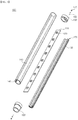
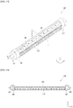
- FIG. 1 , FIG. 2 and FIG. 3 illustrate a tube-shaped LED lighting device according to a first exemplary embodiment of the disclosure.
- FIG. 1 is a part diagram of the tube-shaped LED lighting device according to the first exemplary embodiment of the disclosure.
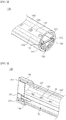
- FIG. 2 is a sectional view of the tube-shaped LED lighting device according to the first exemplary embodiment of the disclosure.
- FIG. 3 is a side sectional view of the tube-shaped LED lighting device according to the first exemplary embodiment of the disclosure.
- the tube-shaped LED lighting device 100 includes a substrate 110, light emitting device 120, a heat sink 130, a cover 140, and a base 150.
- the substrate 110 is a printed circuit board having conductive pattern (not shown) formed thereon.
- the conductive pattern of the substrate 110 is electrically connected to the light emitting device 120.
- the substrate 110 is elongated corresponding to an elongated shape of the cover 140.
- the light emitting device 120 is mounted on one surface of the substrate 110.
- the light emitting device 120 may include an LED chip (not shown) and a phosphor (not shown).
- the light emitting device 120 may generate various colors including white through combination of the LED chip and the phosphor.
- plural light emitting devices 120 are mounted on the substrate 110. However, it should be noted that the number of light emitting device 120 mounted on the substrate 110 may be changed according to user selection, as needed.
- the heat sink 130 serves to dissipate heat from the light emitting device 120 and the substrate 110.
- the heat sink 130 includes a substrate holding portion 131, groove portions 133, and heat dissipation fin 135.
- the substrate holding portion 131 is formed on one surface of the heat sink 130, on which the substrate 110 is seated, to surround opposite sides of the substrate 110 seated on the heat sink.
- the substrate holding portion 131 is elongated in the longitudinal direction of the heat sink 130.
- One surface 132 of the substrate holding portion 131 has a gradually increasing height from an inner side of the heat sink 130, on which the substrate 110 is seated, toward an outer side thereof. That is, the one surface 132 of the substrate holding portion 131 is formed to have a certain angle.
- the one surface 132 of the substrate holding portion 131 is an upper surface with reference to FIG. 1 .
- the certain angle is defined to prevent light emitted from the light emitting device 120 from being shielded by the substrate holding portion 131. With this structure, the substrate holding portion 131 secures high luminous efficacy of the tube-shaped LED lighting device 100.
- the groove portion 133 is formed on opposite side surfaces of the heat sink 130.
- the groove portion 133 is concavely formed in a groove shape on the heat sink 130.
- the groove portion 133 has a shape corresponding to the overhang 141 of the cover 140.
- the groove portion 133 is placed corresponding to the overhang 141 of the cover 140. The overhang 141 of the cover 140 is inserted into the groove portion 133 such that the heat sink 130 is coupled to the cover 140.
- the heat dissipation fin 135 is formed on a lower side of the heat sink 130.
- the heat sink 130 may have a plurality of heat dissipation fins 135. With this structure, the heat dissipation fin 135 increases a contact area between the heat sink 130 and air to improve heat dissipation performance of the heat sink 130.
- the structure of heat dissipation fin 135 may be modified in various ways, as needed.
- a side surface of the heat sink 130 is formed corresponding to an inner wall of the cover 140.
- the cover 140 has a cylindrical shape and thus has a curved inner wall. Accordingly, the side surface of the heat sink 130 has a curved shape.
- Such a structure can minimize a separation distance between the cover 140 and the heat sink 130. As the separation distance between the cover 140 and the heat sink 130 is decreased, the heat sink 130 can more easily dissipate heat from the light emitting device 120 and the substrate 110 through the cover 140. Accordingly, the tube-shaped LED lighting device 100 has improved heat dissipation performance. Further, as shown in the drawings, the heat dissipation fin 135 has one end formed along the inner wall of the cover 140, thereby enabling heat dissipation through the cover 140.
- the cover 140 is configured to surround the heat sink 130, the substrate 110, and the light emitting device 120. That is, the cover 140 receives the heat sink 130, the substrate 110, and the light emitting device 120 therein.
- the overhang 141 is formed on the cover 140.
- the overhang 141 protrudes from the inner wall of the cover 140 toward an interior space of the cover 140.
- the overhang 141 is inserted into the groove portion 133 formed on the opposite side surfaces of the heat sink 130.
- the cover 140 is formed of a transparent resin or glass.
- at least part of the cover 140 is formed of pure polymethyl methacrylate (PMMA).
- PMMA polymethyl methacrylate
- the pure PMMA refers to PMMA free from an impurity or other components. That is, the entirety of the cover 140 is formed of the pure PMMA.
- the cover 140 may be partially formed of the pure PMMA.
- a portion of the cover 140 formed of the pure PMMA includes a region through which light emitted from the light emitting device passes.
- PMMA has higher light transmittance with decreasing content of impurities or other components therein. Accordingly, a portion of the cover 140, through which light emitted from the light emitting device passes, may be formed of the pure PMMA to improve light transmittance.
- the cover 140 is transparent. However, it should be understood that the cover 140 is not limited thereto.
- the cover 140 may be translucent or may have a color.
- the base 150 is coupled to each of opposite ends of the cover 140.
- the base 150 is formed with cover insertion grooves 151 corresponding to the opposite ends of the cover 140.
- the opposite ends of the cover 140 are inserted into the cover insertion grooves 151 of the base 150, so that the cover 140 is coupled to the base 150.
- the cover 140 is secured to the bases 150 in a coupled state using screws 160.
- One end of the screw 160 is placed inside the base 150 and the other end of the screw 160 is placed inside the cover 140.
- the cover 140 may be secured to the bases 150 in a coupled state using adhesives.
- the present disclosure is not limited to use of the screw or adhesives for securing the cover 140 to the bases 150 in a coupled state.
- the cover 140 may be secured to the bases 150 by any method known in the art.
- a sealing member 170 is inserted into a space between the screw 160 and an outer surface of the tube-shaped LED lighting device 100.
- the sealing member 170 prevents moisture from entering the tube-shaped LED lighting device 100.
- the sealing member 170 may be formed of a resilient material and may be a rubber packing.
- the sealing member 170 may be omitted as needed.
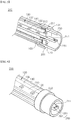
- FIG. 4 to FIG. 6 illustrates a tube-shaped LED lighting device according to a second exemplary embodiment of the disclosure.
- FIG. 4 is a part diagram of a tube-shaped LED lighting device according to a second exemplary embodiment of the disclosure.
- FIG. 5 is a sectional view of the tube-shaped LED lighting device according to the second exemplary embodiment of the disclosure.
- FIG. 6 is a side sectional view of the tube-shaped LED lighting device according to the second exemplary embodiment of the disclosure.
- the tube-shaped LED lighting device 200 includes a substrate 210, light emitting device 120, a heat sink 130, a cover 140, and a base 250.
- the substrate 210, the light emitting device 120 and the heat sink 130 are disposed inside the cover 140.
- the substrate 210 is secured to a substrate holding portion 131 formed on one surface of the heat sink 130.
- the light emitting device 120 is mounted on one surface of the substrate 210.
- the base 250 is coupled to each of opposite ends of the cover 140.
- the base 250 is formed with a cover insertion groove 251. The opposite ends of the cover 140 are inserted into the cover insertion grooves of the bases 250 such that the cover 140 is coupled to the base 250.
- the substrate 210 has one end 211 penetrating the interior of the base 250.
- the base 250 coupled to the one end of the cover 140 is formed with an opening (not shown) penetrating the interior thereof.
- the one end 211 of the substrate 210 is placed inside the base 250 through the opening of the base 250.
- the one end 211 of the substrate 210 placed inside the base 250 is formed with power pad 280.
- the power pad 280 includes a first power pad 281 and a second power pad 282.
- one of the first power pad 281 and the second power pad 282 is connected to a positive electrode of an external power device and the other power pad is connected to a negative electrode thereof.
- both the first power pad 281 and the second power pad 282 are formed on one surface of the substrate 210 to be parallel to each other.
- the power pad 280 is electrically connected to the light emitting device 120 through conductive patterns (not shown) formed on the substrate 210.
- the power pads 280 are connected to an external power device (not shown). That is, the power pad 280 disposed inside the base 250 electrically connect the external power device (not shown) to the light emitting device 120. Connection between the other end of the cover 140 and the base 250 is the same as shown in FIG. 3 .
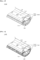
- FIG. 7 to FIG. 9 illustrates tube-shaped LED lighting devices according to third to fifth exemplary embodiments of the disclosure.
- tube-shaped LED lighting devices 300, 400, 500 according to the third to fifth exemplary embodiments of the disclosure from the tube-shaped LED lighting device according to the second exemplary embodiment of the present disclosure.
- the omitted components refer to the description of the tube-shaped LED lighting device according to the second exemplary embodiment of the disclosure.
- FIG. 7 to FIG. 9 a portion of a substrate 210, 510 disposed inside the base 250 is shown.
- the portion of the substrate 210, 510 corresponds to the one end 211 of the substrate 210 described in the second exemplary embodiment with reference to FIG. 4 to FIG. 6 .
- FIG. 7 is a view of a tube-shaped LED lighting device according to a third exemplary embodiment of the disclosure.
- the tube-shaped LED lighting device 300 includes power pad 280 formed on one surface and the other surface of the substrate 110, respectively.
- a first power pad is formed on one surface of the substrate 110 and a second power pad is formed on the other surface of the substrate 110.
- FIG. 8 is a view of the tube-shaped LED lighting device according to the fourth exemplary embodiment of the disclosure.
- the tube-shaped LED lighting device 400 includes power pad 280 formed on one end of the substrate 110. That is, a first power pad 281 and a second power pad 282 are formed on one end of the substrate 110 to be parallel to each other.
- FIG. 9 is a view of a tube-shaped LED lighting device according to a fifth exemplary embodiment of the disclosure.
- the tube-shaped LED lighting device 500 includes a substrate 510, one end of which is formed to have a separation space. That is, the one end of the substrate 510 is bifurcated into two portions.
- the tube-shaped LED device 500 includes power pad 280 formed on the bifurcated portions of the substrate 510, respectively. Specifically, as shown in FIG. 9 , a first power pad 281 and a second power pad 282 are disposed on the bifurcated portions of the substrate 510, respectively.
- FIG. 4 to FIG. 9 Various embodiments of the substrate and the power pad are illustrated with reference to FIG. 4 to FIG. 9 .
- the structures of the substrate and the power pad according to the present disclosure are not limited thereto.
- One end of the substrate may be modified to facilitate connection to the external power device.
- the location and structure of the power pad may be modified to facilitate connection to the external power device.
- FIG. 10 and FIG. 11 illustrate a tube-shaped LED lighting device according to a sixth exemplary embodiment of the disclosure.
- FIG. 10 is a side sectional-view of the tube-shaped LED lighting device according to the sixth exemplary embodiment of the disclosure.
- FIG. 11 is a sectional view of a tube-shaped LED lighting device according to the sixth exemplary embodiment of the disclosure.
- one end 211 and the other end of a substrate 210 are placed inside bases 250.
- only one end of the substrate 210 may be placed inside the base 250, as in the other embodiments.
- the one end 211 of the substrate 210 is formed with power pad 280.
- the tube-shaped LED lighting device 600 includes a connector 690.
- the connector 690 is formed with conductive patterns.
- the entirety of both surfaces of the connector 690 may be formed of a conductive material.
- one surface of the connector 690 is electrically insulated from the other surface thereof.
- conductive patterns may be formed on portions of both surfaces of the connector 690 and on the interior of the connector 690. The conductive patterns formed on portions of both surfaces of the connector 690 are formed on opposite ends of the connector 690, respectively.
- One end of the connector 690 contacts the power pad 280 of the substrate 210.
- the conductive patterns electrically connected to the first power pad 281 and the second power pad 282 is insulated from each other.
- the other end of the connector 690 is exposed outside the base 250.
- the other end of the connector 690 exposed outside the base 250 is connected to an external power device (not shown).
- the substrate 210 is electrically connected to the external power device through the connector 690.
- FIG. 12 to FIG. 14 illustrates tube-shaped LED lighting devices according to seventh to ninth exemplary embodiments of the disclosure.
- tube-shaped LED lighting devices 700, 800, 900 according to the seventh to ninth exemplary embodiments of the disclosure from the tube-shaped LED lighting device according to the sixth exemplary embodiment of the disclosure.
- the omitted components refer to the description of the tube-shaped LED lighting device according to the sixth exemplary embodiment of the disclosure.
- FIG. 12 is a view of a tube-shaped LED lighting device according to a seventh exemplary embodiment of the disclosure.
- the tube-shaped LED lighting device 700 includes a first power pad 281 and a second power pad 282 formed on one surface of the substrate 210.
- a connector 790 includes a first connector 791 and a second connector 792.
- the first connector 791 is brought into contact with the first power pad 281 to be electrically connected thereto.
- the second connector 792 is brought into contact with the second power pad 282 to be electrically connected thereto.
- the first connector 791 and the second connector 792 may be formed of a conductive material.
- the first connector 791 and the second connector 792 may be formed with conductive patterns for electrical connection between the substrate 210 and an external power device.
- FIG. 13 is a view of a tube-shaped LED lighting device according to an eighth exemplary embodiment of the disclosure.
- the tube-shaped LED lighting device 800 includes power pad 280 formed on both surfaces of the substrate 210.
- a first power pad is formed on one surface of the substrate 210 and a second power pad is formed on the other surface thereof.
- a first connector 791 is brought into contact with the first power pad to be electrically connected thereto.
- the second connector 792 is brought into contact with the second power pad to be electrically connected thereto.
- the first connector 791 and the second connector 792 may be formed of a conductive material.
- the first connector 791 and the second connector 792 may be formed with conductive patterns for electrical connection between the substrate 210 and an external power device.
- FIG. 14 is a view of the tube-shaped LED lighting device according to the ninth exemplary embodiment of the disclosure.
- the tube-shaped LED lighting device 900 includes power pad 280 formed on opposite side surfaces of the substrate 210.
- a first power pad is formed on one side surface of the substrate 210 and a second power pad is formed on the other side surface thereof.
- a first connector 791 is brought into contact with the first power pad to be electrically connected thereto.
- the second connector 792 is brought into contact with the second power pad to be electrically connected thereto.
- the first connector 791 and the second connector 792 may be formed of a conductive material.
- the first connector 791 and the second connector 792 may be formed with conductive patterns for electrical connection between the substrate 210 and an external power device.
- the power pad may have various structures and may be disposed at various locations on one end of the substrate disposed inside the base. Accordingly, the connector may also have various structures and may be disposed at various locations.
- FIG. 15 is a view of a tube-shaped LED lighting device according to a tenth exemplary embodiment of the disclosure.
- the cover 140 (see FIG. 1 to FIG. 14 ) of the lighting device is illustrated as being formed of a transparent material.
- the present disclosure is not limited to the structure wherein the entirety of the cover 140 (see FIG. 1 to FIG. 14 ) is formed of a transparent material.
- the tube-shaped LED lighting device 1000 includes a cover 1040 formed of a mixture of a transparent material and a non-transparent material.
- the cover 1040 is divided into a first cover 1041 and a second cover 1042.
- the first cover 1041 is a portion of the cover 1040 disposed above the overhang 141. That is, the first cover 1041 includes a portion of the cover through which light emitted from the light emitting device 120 passes.
- the first cover 1041 is formed of a transparent material.
- the first cover 1041 is formed of pure PMMA.
- the second cover 1042 is the overhang 141 of the cover 1040 and a portion of the cover 1040 disposed under the overhang 141. That is, the second cover 1042 is a portion of the cover 1040 excluding the first cover 1041.
- the second cover 1042 is formed of a non-transparent material.
- the first cover 1041 and the second cover 1042 are divided with reference to the overhang 141.
- the reference for dividing the first cover 1041 and the second cover 1042 is not limited to the overhang 141. That is, the reference for dividing the first cover 1041 and the second cover 1042 may be changed by those skilled in the art, as needed, so long as the first cover 1041 allows light emitted from the light emitting device 120 to pass therethrough.
- first cover 1041 and the second cover 1042 may be achieved by any method known in the art.
- first cover 1041 may be integrally formed with the second cover 1042, and the portion of the cover 1040 corresponding to the second cover 1042 may be coated with a non-transparent material.
- FIG. 16 is a view of a tube-shaped LED lighting device according to an eleventh exemplary embodiment of the disclosure.
- the cover 140 (see FIG. 1 to FIG. 14 ) of the LED lighting device is illustrated as being transparent, translucent or colored.
- the present disclosure is not limited to the structure wherein the entirety of the cover 140 (see FIG. 1 to FIG. 14 ) has a single color.
- the cover 1140 may have a mixture of two or more of transparent, translucent, and a colored.
- the cover 1140 is divided into a first cover 1141 and a second cover 1142.
- the first cover 1141 is a portion of the cover 1140 disposed above the overhang 141.
- the second cover 1142 is a portion of the cover 1140 excluding the first cover 1141.
- the first cover 1141 is transparent and the second cover 1142 is translucent or colored.
- the first cover 1141 and the second cover 1142 are not limited thereto.
- the first cover 1141 may be translucent or colored and the second cover 1142 may be transparent.
- the first cover 1141 may be translucent and the second cover 1142 may be colored.
- the first cover 1141 may be colored and the second cover 1142 may be translucent.
- Such a translucent or colored cover 1140 may be formed by coating first transparent cover 1141 and second transparent cover 1142 with a translucent or colored material.
- the translucent or colored cover 1140 may be formed including a material for translucency or coloring.
- first cover 1141 and the second cover 1142 are divided with reference to the overhang 141.
- the reference for dividing the first cover 1141 and the second cover 1142 is not limited to the overhang 141. That is, the reference for dividing the first cover 1141 and the second cover 1142 may be changed by those skilled in the art, as needed.
- the first cover 1141 and the second cover 1142 are divided from each other with reference to color.
- the first cover 1141 is not required to be physically divided from the second cover 1142. That is, the first cover 1141 may be integrally formed with the second cover 1142.
- the cover 1140 may have a mixed color by coating a translucent or colored material on a predetermined portion thereof. Further, the cover 1140 is not required to have a mixed color of two colors. The cover 1140 may have a mixed color of three colors.
- each of the first cover 1041 (see FIG. 15 ), which is transparent, and the second cover 1042, which is non-transparent, (see FIG. 15 ) according to the tenth exemplary embodiment may include at least one of transparent, translucent, and a color ed.
- FIG. 17 is a view of a UV lamp 2100 according to an exemplary embodiment of the disclosure.
- FIG. 18 is a side sectional-view of the UV lamp 2100 shown in FIG. 17 .
- the UV lamp 2100 includes a lamp tube 2110, a printed circuit board 2120, at least one UV light emitting device 2130, bases 2141, 2142, and at least one power pin 2151.
- the lamp tube 2110 includes an upper cover and a lower cover integrally formed with the upper cover.
- the lamp tube 2110 extends in the X direction and defines an interior space of the UV lamp 2100.
- the lamp tube 2110 has a height in the Z direction.
- the lamp tube 2110 may have a cylindrical shape, as shown in FIG. 17 .
- the upper cover 2111 is formed of a transparent material.
- the upper cover 2111 includes polymethyl methacrylate (PMMA) and/or quartz.
- the lower cover 2112 may be formed of an opaque material in order to shield a space corresponding to the lower cover inside the lamp tube 2110.
- the lower cover 2112 may include polymethyl methacrylate and/or quartz.
- the lower cover 2112 may further include at least one of a pigment, a filler, and a similar material thereto.
- the printed circuit board 2120 extends in the X direction and has a width in the Y direction.
- the printed circuit board 2120 is secured inside the lamp tube 2110.
- the printed circuit board 2120 drives at least one UV light emitting device 2130 with power received through the power pin 2151.
- the at least one UV light emitting device 2130 is disposed on the printed circuit board 2120.
- ten UV light emitting devices are arranged on the printed circuit board 2120 in the X direction.
- the UV light emitting device 2130 is disposed to face the upper cover 2111.
- the UV light emitting device 2130 is adapted to emit UV light under control of the printed circuit board.
- the UV light emitting device 2130 may be secured such that UV light emitted therefrom is directed toward the transparent upper cover.
- the UV light emitting device 2130 may be a UV LED.
- the bases 2141, 2142 are secured to opposite distal ends of the lamp tube 2110.
- the bases 2141, 2142 may block the interior of the lamp tube 2110 from the exterior.
- At least one power pin 2151 is secured to the bases 2141, 2142.
- the power pin 2151 is connected to an external connector (not shown) to receive power for operation of the printed circuit board 2120.
- the printed circuit board 2120 may receive DC power through the power pin 2151.
- the UV lamp 2100 may further include a power supply adapted to convert AC power received through the power pin 2151 into DC power. The power supply supplies the converted DC power to the printed circuit board 2120.
- the bases 2141, 2142 may include polycarbonate (PC).
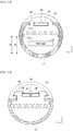
- FIG. 19 is a cross-sectional view of the UV lamp 2100 taken along line I-I' of FIG. 17 .
- the UV lamp 2100 further includes a heat sink 2160.
- the heat sink 2160 is adapted to dissipate heat generated from the printed circuit board 2120 upon operation of the printed circuit board.
- the heat sink 2160 may include a plurality of concavo-convex shapes formed on a lower surface thereof, as shown in FIG. 19 .
- the plurality of concavo-convex shapes increases a surface area of the lower surface of the heat sink 2160, whereby the heat sink 2160 can achieve efficient heat dissipation.
- the heat sink 2160 is secured to the lamp tube 2110.
- the upper cover 2111 and the lower cover 2112 include an overhang 2111_1 and an overhang 2112_1 protruding into the interior space of the UV lamp, and the heat sink 2160 may be secured by the overhangs 2111_1, 2112_1.
- the heat sink 2160 may have a groove 2161 formed on an upper surface thereof. With the structure wherein the printed circuit board 2120 is placed in the groove 2161, the heat sink 2160 can support the printed circuit board 2120.
- the heat sink 2160 may include at least one protrusion 2162 protruding from an upper portion of the groove 2161 in the Y direction or in an opposite direction to the Y direction. The protrusion 2162 allows the printed circuit board 2120 to be effectively secured to the heat sink 2160.
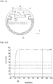
- FIG. 20a is a graph depicting variation in transmittance of the upper cover 2111 including polymethyl methacrylate according to wavelength of light.
- the horizontal axis indicates wavelengths in nanometers (nm) and the vertical axis indicates transmittance.
- the upper cover 2111 including polymethyl methacrylate has a transmittance of 0% at a wavelength of 200 nm.
- the transmittance of the upper cover 2111 rapidly increases at about 300 nm.
- the transmittance of the upper cover 2111 is 90% or greater at a wavelength of about 340 nm and is stably maintained at a value greater than 90% at a wavelength of 360 nm or more.
- the transmittance of the upper cover 2111 is greater than 90% at wavelengths of 400 nm, 500 nm, 600 nm, 700 nm, 800 nm, 900 nm, 1000 nm, and 1100 nm. From this result, it can be understood that polymethyl methacrylate has a critical significance at a wavelength of about 360 nm.
- the UV light emitting device 2130 emits UV light having a wavelength of 360 nm or more toward the upper cover 2111 and the upper cover 2111 includes polymethyl methacrylate.
- the upper cover 2111 allows the UV light to pass therethrough with high transmittance.
- UV light generally has a wavelength of about 100 nm to 400 nm.
- the UV light emitting device 2130 may emit UV light having a predetermined wavelength in the wavelength range of 360 nm to 400 nm.
- the polymethyl methacrylate may have material properties to be deformed at a relatively low temperature.
- UV light having a wavelength of 360 nm or more passes through the upper cover 2111 including polymethyl methacrylate, there can be a problem of deformation of the upper cover 2111 due to heat.
- FIG. 20b is a graph depicting time-dependent variation in transmittance of the upper cover 2111 including polymethyl methacrylate when UV light having a wavelength of 360 nm passes through the upper cover 2111.
- FIG. 21 is a graph depicting variation in transmittance of the upper cover 2111 containing a diffusion agent according to wavelength of light.
- the horizontal axis indicates time and the transverse axis indicates transmittance.
- the transmittance of the upper cover 2111 is maintained at about 90%.
- the transmittance of the upper cover 2111 is about 90%.
- the transmittance of the upper cover 2111 may be changed by about 5% to 10% according to experimental error.
- Retention of high transmittance even upon continuous exposure of the upper cover 2111 to UV light having a wavelength of 360 nm may mean that the upper cover 2111 is not deformed even by continuous exposure to the UV light. For example, even when the upper cover 2111 is continuously exposed to the UV light, the upper cover 2111 does not suffer from discoloration or cracking. This means that use of the UV light cannot easily cause generation of heat from the upper cover 2111. It can be understood that this is because the upper cover 2111 efficiently transmits the UV light instead of absorbing the UV light.
- the upper cover 2111 including polymethyl methacrylate is prevented from being deformed by the provision of the UV light emitting device adapted to emit UV light having a wavelength of 360 nm or more.
- the upper cover 2111 allows UV light having a wavelength of 360 nm or more to pass therethrough with high transmittance without being deformed even if exposed to the UV light for a long time.
- the upper cover 2111 may be free from a diffusion agent for light diffusion or may contain a small amount of the diffusion agent.
- the diffusion agent may be contained in the tube of the lamp emitting visible light.
- the diffusion agent improves uniformity of visible light through diffuse the visible light passing through the tube.
- UV light having a wavelength of 360 nm or more is absorbed and scattered by the diffusion agent, thereby may be reducing transmittance of the upper cover 2111.
- the upper cover 2111 has a transmittance of less than 10% at 360 nm and a transmittance of 90% at 400 nm or more.
- the upper cover 2111 containing the diffusion agent has high transmittance with respect to visible light, and low transmittance with respect to UV light having a wavelength of 360 nm to 400 nm.
- the upper cover 2111 may be free from the diffusion agent or may contain a small amount of the diffusion agent. Accordingly, as described with reference to FIG. 20b , the upper cover 2111 can maintain high transmittance with respect to UV light having a wavelength of 360 nm or more. Furthermore, the upper cover 2111 does not cause absorption and refraction of UV light by the diffusion agent, so the possibility of deformation of the upper cover 2111 by heat can be reduced.
- the upper cover 2111 may be free from an impact reinforcing agent or may contain a small amount of the impact reinforcing agent, for example, acrylic rubbers. As described with reference to FIG. 20b , the upper cover 2111 can maintain high transmittance with respect to UV light having a wavelength of 360 nm or more without absorption of UV light by the impact reinforcing agent.
- the upper cover 2111 may include pure polymethyl methacrylate.
- FIG. 22 is a sectional view of a UV lamp 2100 according to another exemplary embodiment of the disclosure.
- a printed circuit board 2220, a UV light emitting device 2230, a heat sink 2260, and a power supply 2270 are disposed inside an upper cover 2211 and a lower cover 2212.
- the upper cover 2211 has high transmittance with respect to UV light having a wavelength of 360 nm without being deformed thereby. Accordingly, the internal structure of the lamp tube can be modified by placing the heat sink 2260 at a high height HI such that the distance between the UV light emitting device 2230 and the upper cover 2211 is reduced, as compared with the lamp tube according to the exemplary embodiment shown in FIG. 19 .
- the heat sink 2260 may be placed at a location higher than or equal to the height HI thereof.
- the height HI may be greater than a height H2 corresponding to a radius of the lamp tube (2110 of FIG. 17 ). Accordingly, it is possible to secure a region in which the power supply 2270 is placed between the heat sink 2260 and the lower cover 2212.
- the upper cover 2211 may include polymethyl methacrylate and/or quartz, and may be formed to be transparent.
- the lower cover 2212 may include polymethyl methacrylate and/or quartz, and may be formed to be opaque.
- the heat sink 2260 may be secured to the lamp tube in various ways.
- the lower cover 2212 may include first overhang 2212_1 and second overhang 2212_2 protruding toward the interior region of the lamp tube and the heat sink 2260 may be secured to the first overhang 2212_1 and second overhang 2212_2.
- the power supply 2270 is adapted to convert external AC power into DC power and to supply the converted DC power to the printed circuit board 2220.
- the power supply 2270 may be a switched mode power supply (SMPS).
- SMPS switched mode power supply
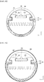
- FIG. 23 is a sectional view of a UV lamp 2100 according to a further exemplary embodiment of the disclosure.
- FIG. 24 is an exploded perspective view showing a printed circuit board 2320, UV light emitting devices 2330, a heat sink 2360, and a flame retardant layer 2380.
- the printed circuit board 2320, the UV light emitting device 2330, the heat sink 2360, and a flame retardant layer 2380 are disposed inside the upper cover 2311 and the lower cover 2312.
- Polymethyl methacrylate contained in the upper cover 2311 may be deformed at a relatively low temperature.
- the printed circuit board 2320 can generate a spark and a flame during operation.
- the flame retardant layer 2380 is disposed between the printed circuit board 2320 and the upper cover 2311.
- the flame retardant layer 2380 may be disposed on the printed circuit board 2320.
- the flame retardant layer 2380 may include a flame retardant substance.
- the flame retardant layer 2380 can protect the upper cover 2311 from the spark and flame generated from the printed circuit board 2320.
- a groove 2361 may be formed on the heat sink 2360.
- the heat sink 2360 may include at least one protrusion 2362 protruding from an upper portion of the groove 2361 in the Y direction or in an opposite direction to the Y direction.
- the printed circuit board 2320 and the flame retardant layer 2380 may be received in the groove 2361 and may be secured by the protrusion 2362.
- the flame retardant layer 2380 includes one or more holes 381. Each of the holes 381 corresponding to each of the UV light emitting devices 2330 on the printed circuit board 2320.
- the flame retardant layer 2380 is attached to the printed circuit board 2320, the UV light emitting device 2330 pass through the hole 381. After attachment of the flame retardant layer 2380, the UV light emitting device 2330 protrudes toward the upper cover 2311 through the flame retardant layer 2380.
- the printed circuit board 2320 and the flame retardant layer 2380 are secured in the groove 2361.
- FIG. 25 is a sectional view of a UV lamp 2100 according to a further exemplary embodiment of the disclosure.
- a printed circuit board 2420, UV light emitting device 2430, a heat sink 2460, and a flame retardant layer 2480 are disposed inside an upper cover 2411 and a lower cover 2412.
- the printed circuit board 2420 is disposed in a groove 2461 formed on the heat sink 2460.
- the flame retardant layer 2480 may be provided to cover an upper side of the heat sink 2460 and the printed circuit board 2420.
- the flame retardant layer 2480 may be secured to the upper side of the heat sink 2460 and the printed circuit board 2420 using adhesives.
- FIG. 26 is a sectional view of the UV lamp taken along line II-II' of FIG. 17 .
- the printed circuit board 2120, the UV light emitting device 2130 and the heat sink 2160 are disposed inside the upper cover 2111 and the lower cover 2112.
- the base 2141 is secured to one end of the lamp tube (2110 of FIG. 17 ).
- the base 2141 may include grooves to receive the upper cover 2111 and the lower cover 2112.
- the base 2141 may include a support 2141_1 protruding in the X direction to support the heat sink 2160.
- the UV light emitting device 2130 may have a predetermined beam range RG.
- the UV light emitting device 2130 may emit UV light within a beam angle of 120°.
- the UV light emitting device 2130 may be disposed such that the base 2141 is placed outside the beam range RG.
- the UV light emitting device 2130 may be separated from the base 2141 such that the base 2141 is placed outside the beam range RG.
- the base 2141 may contain a UV stabilizer.
- the UV stabilizer serves to maintain the properties of the base in a stable state even when the base 2141 is irradiated with UV light.
- the UV stabilizer may include at least one of an absorbent, a quencher, a hindered amine light stabilizer (HALS), and similar materials thereto.
- HALS hindered amine light stabilizer
- FIG. 27 is a view of a modified embodiment 2500 of the UV lamp 2100 shown in FIG. 17 .
- FIG. 28 is a sectional view of the UV lamp 2500 shown in FIG. 27 .
- a portion of the UV lamp 2500 is shown in FIG. 27 and FIG. 28 .
- the lamp tube 2510 includes an upper cover 2511 and a lower cover 2512.
- the upper cover 2511 and the lower cover 2512 have the same configurations as the upper cover 2111 and the lower cover 2112 described with reference to FIG. 17 and FIG. 18 . Repeated descriptions of the same components are omitted in the following.
- a base 2541 is secured to a distal end of the lamp tube 2510.
- the base 2541 may include a support 2541_1 adapted to support a heat sink 2560.
- the UV light emitting device 2530 is disposed on the printed circuit board 2520.
- the printed circuit board 2520 is disposed on the heat sink 2560 and may include a protrusion 2521 protruding therefrom to extend into an interior space of the lamp tube 2510 and penetrating the base 2541.
- the protrusion 2521 may be configured to receive an external connector through which power is supplied to the UV lamp.
- the UV lamp 2500 may receive power through the protrusion 2521.
- the printed circuit board 2520 may receive the DC power through the protrusion 2521.
- the UV lamp 2500 may further include a power supply (2270 of FIG. 22 ) adapted to convert the AC power received through the protrusion 2521 into DC power. The power supply supplies the converted DC power to the printed circuit board 2520.
- FIG. 29 is a sectional view of a UV lamp 2100 according to yet another exemplary embodiment of the disclosure.
- the UV lamp 2100 further includes a flame retardant layer 2180.
- the flame retardant layer 2180 is disposed on an inner surface of the lamp tube 2110.
- the printed circuit board 2120, the UV light emitting device 2130 and/or the heat sink 2160 may generate and/or transfer heat, the heat may be transferred to the lamp tube 2110.
- the lamp tube 2110 further includes the flame retardant layer 2180 attached to at least a portion of the inner surface thereof. Accordingly, the lamp tube 2110 and/or the UV lamp 2100 can be prevented from being deformed or burnt.
- the flame retardant layer 2180 may be disposed over the entirety of the inner surface of the lamp tube 2110. In an alternative embodiment, the flame retardant layer 2180 may be disposed on a portion of the inner surface of the lamp tube 2110.
- the flame retardant layer 2180 may contain fluorine.
- FIG. 30 is a sectional view of the UV lamp 2100 according to yet another exemplary embodiment of the disclosure.
- the flame retardant layer 2190 may surround at least a portion of an outer surface of the lamp tube 2110.
- the flame retardant layer 2190 may be disposed over the entirety of the outer surface of the lamp tube 2110.
- the flame retardant layer 2190 may be disposed on a portion of the outer surface of the lamp tube 2110. Accordingly, the lamp tube 2110 and/or the UV lamp 2100 can be prevented from being deformed or burnt.
- the flame retardant layer 2190 supports the lamp tube 2110 by surrounding the lamp tube 2110, thereby preventing the lamp tube 2110 from being broken and scattered by external impact. For example, such an advantage becomes more apparent when the lamp tube 2110 includes, for example, quartz which can be easily broken.
- FIG. 31 is a flowchart of a method of manufacturing the lamp tube 2100 shown in FIG. 17 .
- a first raw material corresponding to an upper cover (2111 of FIG. 18 ) and a second raw material corresponding to a lower cover (2112 of FIG. 18 ) are prepared.
- the first raw material and the second raw material may be provided to different hoppers, respectively.
- the first raw material includes polymethyl methacrylate and/or quartz.
- the first raw material may be free from a diffusion agent for light diffusion or may contain a small amount of the diffusion agent.
- the first raw material may be free from an impact reinforcing agent or may contain a small amount of the impact reinforcing agent.
- the second raw material may include polymethyl methacrylate and/or quartz, and materials for imparting a color to the lower cover 2112, for example, a pigment, a filler, or a similar material thereto.
- the first raw material is melted to form a first molten material and the second raw material is melted to form a second molten material.
- the first molten material and the second molten material may be generated in different cylinders, respectively.
- the corresponding raw materials may be supplied to the cylinders through the corresponding hoppers. In each of the cylinder, the raw material is delivered, melted and compressed under a suitable pressure to generate the molten material.
- the first molten material and the second molten material are formed to pass through a single mold.
- the first molten material and the second molten material delivered through different cylinders will pass through a single mold.
- the upper cover and the lower cover may be molded by a profile extrusion process.
- the mold may have one of various shapes.
- the mold may have a shape corresponding to the upper cover 2111 and the lower cover 2112 shown in FIG. 19 .
- the mold may have a shape corresponding to the upper cover 211 and the lower cover 212 shown in FIG. 22 .
- the first molten material and the second molten material are forced to pass through a single mold, whereby a transparent upper cover 2111 and a translucent lower cover 2112 can be integrally formed with each other.
- the upper cover 2111 and the lower cover 2112 are cooled to provide a lamp tube 2110.
- the upper cover 2111 and the lower cover 2112 may be cooled by cooling water so as to maintain a molded shape.
- the lamp tube 2110 may be cut to have a suitable length.
- a printed circuit board (2120 of FIG. 19 ), UV light emitting device (2130 of FIG. 19 ), and a heat sink (2160 of FIG. 19 ) are disposed inside the lamp tube 2110.
- the UV lamp includes UV light emitting device emitting UV light having a wavelength of 360 nm or more toward the upper cover, which includes polymethyl methacrylate.
- the upper cover is not deformed when exposed to the UV light for a long period of time while allowing the UV light to pass therethrough. Accordingly, it is possible to provide a UV lamp having improved performance and reliability.
- the tube-shaped LED lighting device has a short distance between the heat sink and the cover, thereby improving heat dissipation. Further, one end of the substrate having the electrode formed thereon is placed inside the base, whereby the tube-shaped LED lighting device can be electrically connected to an external power device without wire bonding. Accordingly, the tube-shaped LED lighting device can be manufactured by a simple process through omission of wire bonding and can prevent failure due to open circuit and short circuit due to wire bonding.
Landscapes
- Engineering & Computer Science (AREA)
- General Engineering & Computer Science (AREA)
- Physics & Mathematics (AREA)
- Microelectronics & Electronic Packaging (AREA)
- Optics & Photonics (AREA)
- Power Engineering (AREA)
- Non-Portable Lighting Devices Or Systems Thereof (AREA)
- Arrangement Of Elements, Cooling, Sealing, Or The Like Of Lighting Devices (AREA)
- Fastening Of Light Sources Or Lamp Holders (AREA)
Abstract
Description
- Exemplary embodiments of the disclosure relate to a tube-shaped LED lighting device.
- Generally, a light emitting diode (LED) refers to a semiconductor device configured to emit light upon application of electric current thereto. The LED is a solid device with various advantages of environmentally friendliness due to no use of mercury, long lifespan and low power consumption and has attracted attention as a new light source.
- Various lighting devices using such an LED as a light source have been developed and an LED lighting device provided with a light bulb type power connector capable of being mounted on a receptacle of a light bulb is spotlighted in the art.
- LEDs have a problem of heat generation in operation. Inefficient heat dissipation of the LEDs can cause deterioration in lifespan and intensity of illumination. An upper temperature limit for efficient turn-on of the LEDs is about 60°C and it is believed that performance of an LED lighting device is directly related to heat dissipation.
- Ultraviolet (UV) light generally refers to light in the wavelength band of 100 nm to 400 nm and has higher energy than visible light. UV light emitted from the sun is divided into ultraviolet-A, ultraviolet-B, and ultraviolet-C, and it is known in the art that most UV-C is absorbed by the ozone layer and UV-A and UV-B reach the ground.
- UV light can be utilized in various fields. A UV lamp includes a lamp tube and a lighting device disposed in the lamp tube and emitting UV light. The lamp tube is required to have high transmittance with respect to UV light and not to be deformed when exposed to UV light for a long period of time.
- Exemplary embodiments of the disclosure provide a tube-shaped LED lighting device with improved heat dissipation.
- Exemplary embodiments of the disclosure provide a tube-shaped LED lighting device free from wire bonding to prevent failure due to open circuit and short circuit.
- Exemplary embodiments of the disclosure provide a UV lamp having improved performance and reliability and a method of manufacturing the same.
- In accordance with one aspect of the present disclosure, a tube-shaped LED lighting device includes: a substrate; a light emitting device mounted on the substrate; a heat sink having one surface on which the substrate is seated, the heat sink including a groove portion formed on opposite side surfaces thereof; a cover receiving the heat sink, the substrate and the light emitting device therein and including an overhang protruding from an inner wall thereof to be inserted into the groove portion; and a base coupled to each of opposite ends of the cover, wherein the opposite side surfaces of the heat sink have a shape corresponding to the inner wall of the cover.
- In accordance with another aspect of the present disclosure, a tube-shaped LED lighting device includes: a substrate; a light emitting device mounted on the substrate; a heat sink having one surface on which the substrate is seated, the heat sing including a groove portion formed on opposite side surfaces thereof; a cover receiving the heat sink, the substrate and the light emitting device therein, and including an overhang protruding from an inner wall thereof to be inserted into the groove portion; and a base coupled to each of opposite ends of the cover, wherein the substrate has one end placed inside the base after passing through the base.
- In accordance with a further aspect of the present disclosure, a UV lamp includes: a lamp tube including an upper cover and a lower cover integrally formed with the upper cover; a printed circuit board secured inside the lamp tube; and at least one UV light emitting device disposed on the printed circuit board to face the upper cover and operated under control of the printed circuit board, wherein the at least one UV light emitting device emits UV light having a wavelength of 360 nm or more toward the upper cover, the upper cover comprising polymethyl methacrylate.
- In one embodiment, the UV lamp may further include a flame retardant layer disposed between the printed circuit board and the upper cover.
- In one embodiment, the UV lamp may further include a heat sink secured inside the lamp tube and adapted to dissipate heat generated from the printed circuit board. The heat sink may be formed at an upper portion thereof with a groove, the printed circuit board and the flame retardant layer may be placed in the groove, and the flame retardant layer may cover the printed circuit board.
- In one embodiment, the UV lamp may further include a heat sink secured inside the lamp tube and adapted to dissipate heat generated from the printed circuit board. The heat sink may be formed at an upper side thereof with a groove, the printed circuit board may be placed in the groove, and the flame retardant layer may cover the upper side of the heat sink and the printed circuit board.
- In one embodiment, the UV lamp may further include: a heat sink adapted to support the printed circuit board and to dissipate heat generated from the printed circuit board; and a power supply disposed between the heat sink and the lower cover and adapted to convert external AC power into DC power and to supply the converted DC power to the printed circuit board. The lower cover may include polymethyl methacrylate and be opaque.
- In one embodiment, the UV lamp may further include a base secured to a distal end of the lamp tube. The at least one UV light emitting device may be disposed on the printed circuit board such that UV light is emitted therefrom in a certain beam orientation range and the base is disposed outside the certain beam orientation range.
- In one embodiment, the UV lamp may further include a base secured to a distal end of the lamp tube. Here, the base may include a UV stabilizer.
- In accordance with yet another aspect of the present disclosure, a UV lamp includes: a lamp tube including an upper cover and a lower cover integrally formed with the upper cover; a printed circuit board secured inside the lamp tube; at least one UV light emitting device disposed on the printed circuit board to face the upper cover and emitting UV light toward the upper cover under control of the printed circuit board; and a flame retardant layer disposed between the printed circuit board and the upper cover. The upper cover may include polymethyl methacrylate.
- In one embodiment, the at least one UV light emitting device may emit UV light having a wavelength of 360 nm or more.
- In one embodiment, the lower cover may include polymethyl methacrylate and may be opaque.
- In accordance with yet another aspect of the present disclosure, a method of manufacturing a UV lamp is provided. The method of manufacturing a UV lamp includes: melting a first raw material and a second raw material to form a first molten material and a second molten material; supplying the first molten material and the second molten material to one mold to integrally form an upper cover and a lower cover; cooling the upper cover and the lower cover; placing a printed circuit board and at least one UV light emitting device operated under control of the printed circuit board inside the upper cover and the lower cover. The at least one UV light emitting device may be disposed to face the upper cover; the at least one UV light emitting device emits UV light having a wavelength of 360 nm toward the upper cover; and the upper cover includes polymethyl methacrylatepolymethyl methacrylate.
- In accordance with yet another aspect of the present disclosure, a UV lamp includes: a lamp tube including an upper cover and a lower cover integrally formed with the upper cover; a printed circuit board secured inside the lamp tube; at least one UV light emitting device disposed on the printed circuit board to face the upper cover and operated to emit UV light toward the upper cover under control of the printed circuit board; and a flame retardant layer disposed between the printed circuit board and the upper cover and surrounding at least part of an outer surface of the lamp tube.
- In one embodiment, the upper cover may include polymethyl methacrylatepolymethyl methacrylate or quartz.
- In one embodiment, the lower cover may include polymethyl methacrylatepolymethyl methacrylate or quartz and may be opaque.
- In one embodiment, the flame retardant layer may be attached to at least part of an inner surface of the lamp tube.
- According to exemplary embodiments of the disclosure, the tube-shaped LED lighting device has a short distance between the heat sink and the cover, thereby improving a heat dissipation function.
- According to the exemplary embodiments of the disclosure, in the tube-shaped LED lighting device, the substrate including electrodes formed thereon has one end disposed inside the base such that the LED lighting device can be electrically connected to an external power device without wire bonding. Accordingly, the tube-shaped LED lighting device can be manufactured by a simple process through omission of wire bonding and can prevent failure due to open circuit and short circuit by wire bonding.
- According to exemplary embodiments of the disclosure, a UV lamp having improved performance and reliability and a method of manufacturing the same are provided.
-
-
FIG. 1 is a parts diagram of a tube-shaped LED lighting device according to a first exemplary embodiment of the disclosure. -
FIG. 2 is a sectional view of the tube-shaped LED lighting device according to the first exemplary embodiment of the disclosure. -
FIG. 3 is a side sectional view of the tube-shaped LED lighting device according to the first exemplary embodiment of the disclosure. -
FIG. 4 is a parts diagram of a tube-shaped LED lighting device according to a second exemplary embodiment of the disclosure. -
FIG. 5 is a sectional view of the tube-shaped LED lighting device according to the second exemplary embodiment of the disclosure. -
FIG. 6 is a side sectional view of the tube-shaped LED lighting device according to the second exemplary embodiment of the disclosure. -
FIG. 7 is a view of a tube-shaped LED lighting device according to a third exemplary embodiment of the disclosure. -
FIG. 8 is a view of a tube-shaped LED lighting device according to a fourth exemplary embodiment of the disclosure. -
FIG. 9 is a view of a tube-shaped LED lighting device according to a fifth exemplary embodiment of the disclosure. -
FIG. 10 is a side sectional-view of a tube-shaped LED lighting device according to a sixth exemplary embodiment of the disclosure. -
FIG. 11 is a sectional view of a tube-shaped LED lighting device according to the sixth exemplary embodiment of the disclosure. -
FIG. 12 is a view of a tube-shaped LED lighting device according to a seventh exemplary embodiment of the disclosure. -
FIG. 13 is a view of a tube-shaped LED lighting device according to an eighth exemplary embodiment of the disclosure. -
FIG. 14 is a view of a tube-shaped LED lighting device according to a ninth exemplary embodiment of the disclosure. -
FIG. 15 is a view of a tube-shaped LED lighting device according to a tenth exemplary embodiment of the disclosure. -
FIG. 16 is a view of a tube-shaped LED lighting device according to an eleventh exemplary embodiment of the disclosure. -
FIG. 17 is a view of a UV lamp according to an exemplary embodiment of the disclosure. -
FIG. 18 is a side sectional-view of the UV lamp shown inFIG. 17 . -
FIG. 19 is a cross-sectional view of the UV lamp taken along line I-I' ofFIG. 17 . -
FIG. 20a is a graph depicting variation in transmittance of an upper cover including polymethyl methacrylatepolymethyl methacrylate according to wavelength of light. -
FIG. 20b is a graph depicting time-dependent variation in transmittance of the upper cover including polymethyl methacrylatepolymethyl methacrylate when UV light having a wavelength of 360 nm passes through the upper cover. -
FIG. 21 is a graph depicting variation in transmittance of the upper cover containing a diffusion agent according to wavelength of light. -
FIG. 22 is a sectional view of a UV lamp according to another exemplary embodiment of the disclosure. -
FIG. 23 is a sectional view of a UV lamp according to a further exemplary embodiment of the disclosure. -
FIG. 24 is an exploded perspective view showing a printed circuit board, UV light emitting devices, a heat sink, and a flame retardant layer. -
FIG. 25 is a sectional view of a UV lamp according to a further exemplary embodiment of the disclosure. -
FIG. 26 is a sectional view of the UV lamp taken along line II-II' ofFIG. 17 . -
FIG. 27 is a view of a modified embodiment of the UV lamp shown inFIG. 17 . -
FIG. 28 is a sectional view of the UV lamp shown inFIG. 27 . -
FIG. 29 is a sectional view of a UV lamp according to yet another exemplary embodiment of the disclosure. -
FIG. 30 is a sectional view of the UV lamp according to yet another exemplary embodiment of the disclosure. -
FIG. 31 is a flowchart of a method of manufacturing the lamp tube shown inFIG. 17 . - It should be understood that the description in Background Art is only for understanding of the background technique of the present disclosure and is not to be construed as corresponding to the prior art known to those skilled in the art.
- In the following description, for the purposes of description, numerous specific details are set forth in order to provide a thorough understanding of various embodiments. It is apparent, however, that various embodiments may be practiced without these specific details or with one or more equivalent arrangements. In other instances, well-known structures and devices are shown in block diagram form in order to avoid unnecessarily obscuring various embodiments.
- In the accompanying figures, the size and relative sizes of layers, films, panels, regions, etc., may be exaggerated for clarity and descriptive purposes. Also, like reference numerals denote like elements.
- When an element or layer is referred to as being "on," "connected to," or "coupled to" another element or layer, it may be directly on, connected to, or coupled to the other element or layer or intervening elements or layers may be present. When, however, an element or layer is referred to as being "directly on," "directly connected to," or "directly coupled to" another element or layer, there are no intervening elements or layers present. For the purposes of this disclosure, "at least one of X, Y, and Z" and "at least one selected from the group consisting of X, Y, and Z" may be construed as X only, Y only, Z only, or any combination of two or more of X, Y, and Z, such as, for instance, XYZ, XYY, YZ, and ZZ. Like numbers refer to like elements throughout. As used herein, the term "and/or" includes any and all combinations of one or more of the associated listed items.
- Although the terms first, second, etc. may be used herein to describe various elements, components, regions, layers, and/or sections, these elements, components, regions, layers, and/or sections should not be limited by these terms. These terms are used to distinguish one element, component, region, layer, and/or section from another element, component, region, layer, and/or section. Thus, a first element, component, region, layer, and/or section discussed below could be termed a second element, component, region, layer, and/or section without departing from the teachings of the present disclosure.
- Spatially relative terms, such as "beneath," "below," "lower," "above," "upper," and the like, may be used herein for descriptive purposes, and, thereby, to describe one element or feature's relationship to another element(s) or feature(s) as illustrated in the drawings. Spatially relative terms are intended to encompass different orientations of an apparatus in use, operation, and/or manufacture in addition to the orientation depicted in the drawings. For example, if the apparatus in the drawings is turned over, elements described as "below" or "beneath" other elements or features would then be oriented "above" the other elements or features. Thus, the exemplary term "below" can encompass both an orientation of above and below. Furthermore, the apparatus may be otherwise oriented (e.g., rotated 90 degrees or at other orientations), and, as such, the spatially relative descriptors used herein should be interpreted accordingly.
- The terminology used herein is for the purpose of describing particular embodiments and is not intended to be limiting. As used herein, the singular forms, "a," "an," and "the" are intended to include the plural forms as well, unless the context clearly indicates otherwise. Moreover, the terms "comprises," "comprising," "includes," and/or "including," when used in this specification, specify the presence of stated features, integers, steps, operations, elements, components, and/or groups thereof, but do not preclude the presence or addition of one or more other features, integers, steps, operations, elements, components, and/or groups thereof.
- A tube-shaped LED lighting device according to one exemplary embodiment of the present disclosure includes: a substrate, a light emitting device mounted on the substrate, a heat sink having one surface on which the substrate is seated, the heat sink including a groove portion formed on opposite side surfaces thereof, a cover receiving the heat sink, the substrate and the light emitting device therein, the cover including an overhang protruding from an inner wall thereof to be inserted into the groove portion, and a base coupled to each of opposite ends of the cover. Here, opposite side surfaces of the heat sink have a shape corresponding to an inner wall of the cover. For example, the inner wall of the cover includes a curved surface. In addition, the opposite side surfaces of the heat sink include curved surfaces. This structure can minimize a distance between the cover and the heat sink. Accordingly, the heat sink facilitates transfer of heat from the light emitting device to the cover, thereby improving heat dissipation of the tube-shaped LED lighting device.
- The heat sink further includes a substrate holding portion surrounding opposite sides of the substrate. One surface of the substrate holding portion has a gradually increasing height from an inner side of the heat sink, on which the substrate is seated, toward an outer side thereof. That is, the one surface of the substrate holding portion is formed to have a certain angle. This structure can prevent light emitted from the light emitting device from colliding with the substrate holding portion, thereby improving luminous efficacy of the tube-shaped LED lighting device.
- The heat sink further includes a heat dissipation fin formed on the other surface thereof facing the one surface thereof. The heat dissipation fin increase a contact area between the heat sink and air, thereby further improving heat dissipation of the tube-shaped LED lighting device.
- The cover is formed of a transparent material. Alternatively, some portion of the cover may be formed of a transparent material and the other portion of the cover may be formed of a non-transparent material. At least part of the cover is formed of pure polymethyl methacrylate (PMMA). That is, a portion of the cover through which light emitted from the light emitting device passes may be formed of pure PMMA. As such, a light transmitting portion of the cover is formed of pure PMMA, thereby improving light transmittance.
- The cover may be formed of a color including at least one of transparent, translucent, and colored.
- The substrate has one end placed inside the base after passing through the base. In addition, power pads are formed on the one end of the substrate placed inside the base. The power pads are connected to an external power device. Due to the substrate and the power pads with this structure, the LED lighting device can omit base heat dissipation fin and a wire for electric connection between the external power device and the substrate in the art. Thus, it is possible to omit a process for inserting the base heat dissipation fin into the base and a wire bonding process. In addition, the LED lighting device can prevent open circuit and short circuit due to failure of the base heat dissipation fin and the wire.
- The power pads may be formed on one surface of the one end of the substrate. Alternatively, the power pads may be formed on one surface and the other surface of the one end of the substrate, respectively. Alternatively, the power pads may be formed on opposite side surfaces of the one end of the substrate, respectively.
- The tube-shaped LED lighting device may further include a connector having one end protruding to outside of the base and the other end contacting the power pads formed on the one end of the substrate.
- A tube-shaped LED lighting device according to another exemplary embodiment of the present disclosure includes: a substrate, a light emitting device mounted on the substrate, a heat sink having one surface on which the substrate is seated, the heat sink including a groove portion formed on opposite side surfaces thereof, a cover receiving the heat sink, the substrate and the light emitting device therein, the cover including an overhang protruding from an inner wall thereof to be inserted into the groove portion, and a base coupled to each of opposite ends of the cover, wherein the substrate has one end placed inside the base after passing through the base.
-
FIG. 1 ,FIG. 2 and FIG. 3 illustrate a tube-shaped LED lighting device according to a first exemplary embodiment of the disclosure.FIG. 1 is a part diagram of the tube-shaped LED lighting device according to the first exemplary embodiment of the disclosure. In addition,FIG. 2 is a sectional view of the tube-shaped LED lighting device according to the first exemplary embodiment of the disclosure. Further,FIG. 3 is a side sectional view of the tube-shaped LED lighting device according to the first exemplary embodiment of the disclosure. - Referring to
FIG. 1 to FIG. 3 , the tube-shapedLED lighting device 100 according to the first exemplary embodiment includes asubstrate 110, light emittingdevice 120, aheat sink 130, acover 140, and abase 150. - The
substrate 110 is a printed circuit board having conductive pattern (not shown) formed thereon. The conductive pattern of thesubstrate 110 is electrically connected to thelight emitting device 120. According to this embodiment, thesubstrate 110 is elongated corresponding to an elongated shape of thecover 140. - The
light emitting device 120 is mounted on one surface of thesubstrate 110. Thelight emitting device 120 may include an LED chip (not shown) and a phosphor (not shown). Thelight emitting device 120 may generate various colors including white through combination of the LED chip and the phosphor. InFIG. 1 to FIG. 3 , plurallight emitting devices 120 are mounted on thesubstrate 110. However, it should be noted that the number of light emittingdevice 120 mounted on thesubstrate 110 may be changed according to user selection, as needed. - The
heat sink 130 serves to dissipate heat from thelight emitting device 120 and thesubstrate 110. Theheat sink 130 includes asubstrate holding portion 131,groove portions 133, andheat dissipation fin 135. - The
substrate holding portion 131 is formed on one surface of theheat sink 130, on which thesubstrate 110 is seated, to surround opposite sides of thesubstrate 110 seated on the heat sink. Thesubstrate holding portion 131 is elongated in the longitudinal direction of theheat sink 130. - One
surface 132 of thesubstrate holding portion 131 has a gradually increasing height from an inner side of theheat sink 130, on which thesubstrate 110 is seated, toward an outer side thereof. That is, the onesurface 132 of thesubstrate holding portion 131 is formed to have a certain angle. Here, the onesurface 132 of thesubstrate holding portion 131 is an upper surface with reference toFIG. 1 . In addition, the certain angle is defined to prevent light emitted from thelight emitting device 120 from being shielded by thesubstrate holding portion 131. With this structure, thesubstrate holding portion 131 secures high luminous efficacy of the tube-shapedLED lighting device 100. - The
groove portion 133 is formed on opposite side surfaces of theheat sink 130. Thegroove portion 133 is concavely formed in a groove shape on theheat sink 130. Here, thegroove portion 133 has a shape corresponding to theoverhang 141 of thecover 140. In addition, thegroove portion 133 is placed corresponding to theoverhang 141 of thecover 140. Theoverhang 141 of thecover 140 is inserted into thegroove portion 133 such that theheat sink 130 is coupled to thecover 140. - The
heat dissipation fin 135 is formed on a lower side of theheat sink 130. Theheat sink 130 may have a plurality ofheat dissipation fins 135. With this structure, theheat dissipation fin 135 increases a contact area between theheat sink 130 and air to improve heat dissipation performance of theheat sink 130. The structure ofheat dissipation fin 135 may be modified in various ways, as needed. - A side surface of the
heat sink 130 is formed corresponding to an inner wall of thecover 140. Referring toFIG. 1 to FIG. 3 , thecover 140 has a cylindrical shape and thus has a curved inner wall. Accordingly, the side surface of theheat sink 130 has a curved shape. Such a structure can minimize a separation distance between thecover 140 and theheat sink 130. As the separation distance between thecover 140 and theheat sink 130 is decreased, theheat sink 130 can more easily dissipate heat from thelight emitting device 120 and thesubstrate 110 through thecover 140. Accordingly, the tube-shapedLED lighting device 100 has improved heat dissipation performance. Further, as shown in the drawings, theheat dissipation fin 135 has one end formed along the inner wall of thecover 140, thereby enabling heat dissipation through thecover 140. - The
cover 140 is configured to surround theheat sink 130, thesubstrate 110, and thelight emitting device 120. That is, thecover 140 receives theheat sink 130, thesubstrate 110, and thelight emitting device 120 therein. Theoverhang 141 is formed on thecover 140. Theoverhang 141 protrudes from the inner wall of thecover 140 toward an interior space of thecover 140. Theoverhang 141 is inserted into thegroove portion 133 formed on the opposite side surfaces of theheat sink 130. - The
cover 140 is formed of a transparent resin or glass. For example, at least part of thecover 140 is formed of pure polymethyl methacrylate (PMMA). Here, the pure PMMA refers to PMMA free from an impurity or other components. That is, the entirety of thecover 140 is formed of the pure PMMA. Alternatively, thecover 140 may be partially formed of the pure PMMA. Here, a portion of thecover 140 formed of the pure PMMA includes a region through which light emitted from the light emitting device passes. PMMA has higher light transmittance with decreasing content of impurities or other components therein. Accordingly, a portion of thecover 140, through which light emitted from the light emitting device passes, may be formed of the pure PMMA to improve light transmittance. - According to this embodiment, the
cover 140 is transparent. However, it should be understood that thecover 140 is not limited thereto. Thecover 140 may be translucent or may have a color. - The
base 150 is coupled to each of opposite ends of thecover 140. For example, thebase 150 is formed withcover insertion grooves 151 corresponding to the opposite ends of thecover 140. The opposite ends of thecover 140 are inserted into thecover insertion grooves 151 of thebase 150, so that thecover 140 is coupled to thebase 150. In addition, thecover 140 is secured to thebases 150 in a coupled state using screws 160. One end of thescrew 160 is placed inside thebase 150 and the other end of thescrew 160 is placed inside thecover 140. Alternatively, thecover 140 may be secured to thebases 150 in a coupled state using adhesives. However, it should be understood that the present disclosure is not limited to use of the screw or adhesives for securing thecover 140 to thebases 150 in a coupled state. Thecover 140 may be secured to thebases 150 by any method known in the art. - A sealing
member 170 is inserted into a space between thescrew 160 and an outer surface of the tube-shapedLED lighting device 100. The sealingmember 170 prevents moisture from entering the tube-shapedLED lighting device 100. For example, the sealingmember 170 may be formed of a resilient material and may be a rubber packing. The sealingmember 170 may be omitted as needed. -
FIG. 4 to FIG. 6 illustrates a tube-shaped LED lighting device according to a second exemplary embodiment of the disclosure.FIG. 4 is a part diagram of a tube-shaped LED lighting device according to a second exemplary embodiment of the disclosure.FIG. 5 is a sectional view of the tube-shaped LED lighting device according to the second exemplary embodiment of the disclosure.FIG. 6 is a side sectional view of the tube-shaped LED lighting device according to the second exemplary embodiment of the disclosure. - Descriptions of components of the tube-shaped
LED lighting device 200 according to the second exemplary embodiment having the same configuration as those of the tube-shaped LED lighting device according to the first exemplary embodiment will be omitted. For the omitted components, refer to the description of the tube-shaped LED lighting device according to the first exemplary embodiment of the disclosure. - Referring to
FIG. 4 to FIG. 6 , the tube-shapedLED lighting device 200 includes asubstrate 210, light emittingdevice 120, aheat sink 130, acover 140, and abase 250. - The
substrate 210, thelight emitting device 120 and theheat sink 130 are disposed inside thecover 140. Here, thesubstrate 210 is secured to asubstrate holding portion 131 formed on one surface of theheat sink 130. In addition, thelight emitting device 120 is mounted on one surface of thesubstrate 210. Further, thebase 250 is coupled to each of opposite ends of thecover 140. For example, thebase 250 is formed with acover insertion groove 251. The opposite ends of thecover 140 are inserted into the cover insertion grooves of thebases 250 such that thecover 140 is coupled to thebase 250. - According to this embodiment, the
substrate 210 has oneend 211 penetrating the interior of thebase 250. The base 250 coupled to the one end of thecover 140 is formed with an opening (not shown) penetrating the interior thereof. The oneend 211 of thesubstrate 210 is placed inside the base 250 through the opening of thebase 250. - The one
end 211 of thesubstrate 210 placed inside thebase 250 is formed withpower pad 280. For example, thepower pad 280 includes afirst power pad 281 and asecond power pad 282. Here, one of thefirst power pad 281 and thesecond power pad 282 is connected to a positive electrode of an external power device and the other power pad is connected to a negative electrode thereof. InFIG. 4 to FIG. 6 , both thefirst power pad 281 and thesecond power pad 282 are formed on one surface of thesubstrate 210 to be parallel to each other. - The
power pad 280 is electrically connected to thelight emitting device 120 through conductive patterns (not shown) formed on thesubstrate 210. In addition, thepower pads 280 are connected to an external power device (not shown). That is, thepower pad 280 disposed inside the base 250 electrically connect the external power device (not shown) to thelight emitting device 120. Connection between the other end of thecover 140 and thebase 250 is the same as shown inFIG. 3 . - Conventionally, electrical connection between the external power device and the substrate on which the light emitting device is mounted requires insertion of a base heat dissipation fin and a wire bonding process. However, such a process is performed in a narrow inner space of the base, thereby causing a failure such as electrical open circuit or short circuit.
- However, according to the exemplary embodiments of the disclosure, it is possible to omit insertion of the base heat dissipation fin and the wire bonding process, thereby simplifying the manufacturing process. In addition, it is possible to prevent occurrence of a failure such as electrical open circuit and short circuit.
-
FIG. 7 to FIG. 9 illustrates tube-shaped LED lighting devices according to third to fifth exemplary embodiments of the disclosure. - The following description will focus on different features of tube-shaped
LED lighting devices - In
FIG. 7 to FIG. 9 , a portion of asubstrate base 250 is shown. The portion of thesubstrate end 211 of thesubstrate 210 described in the second exemplary embodiment with reference toFIG. 4 to FIG. 6 . -
FIG. 7 is a view of a tube-shaped LED lighting device according to a third exemplary embodiment of the disclosure. - Referring to
FIG. 7 , the tube-shapedLED lighting device 300 according to the third exemplary embodiment includespower pad 280 formed on one surface and the other surface of thesubstrate 110, respectively. For example, a first power pad is formed on one surface of thesubstrate 110 and a second power pad is formed on the other surface of thesubstrate 110. -
FIG. 8 is a view of the tube-shaped LED lighting device according to the fourth exemplary embodiment of the disclosure. - Referring to
FIG. 8 , the tube-shapedLED lighting device 400 according to the fourth exemplary embodiment includespower pad 280 formed on one end of thesubstrate 110. That is, afirst power pad 281 and asecond power pad 282 are formed on one end of thesubstrate 110 to be parallel to each other. -
FIG. 9 is a view of a tube-shaped LED lighting device according to a fifth exemplary embodiment of the disclosure. - Referring to
FIG. 9 , the tube-shapedLED lighting device 500 according to the fifth exemplary embodiment includes asubstrate 510, one end of which is formed to have a separation space. That is, the one end of thesubstrate 510 is bifurcated into two portions. The tube-shapedLED device 500 includespower pad 280 formed on the bifurcated portions of thesubstrate 510, respectively. Specifically, as shown inFIG. 9 , afirst power pad 281 and asecond power pad 282 are disposed on the bifurcated portions of thesubstrate 510, respectively. - Various embodiments of the substrate and the power pad are illustrated with reference to
FIG. 4 to FIG. 9 . However, it should be understood that the structures of the substrate and the power pad according to the present disclosure are not limited thereto. One end of the substrate may be modified to facilitate connection to the external power device. Further, the location and structure of the power pad may be modified to facilitate connection to the external power device. -
FIG. 10 andFIG. 11 illustrate a tube-shaped LED lighting device according to a sixth exemplary embodiment of the disclosure.FIG. 10 is a side sectional-view of the tube-shaped LED lighting device according to the sixth exemplary embodiment of the disclosure.FIG. 11 is a sectional view of a tube-shaped LED lighting device according to the sixth exemplary embodiment of the disclosure. - The following description will focus on different features of the tube-shaped
LED lighting device 600 according to the sixth exemplary embodiment of the disclosure from the tube-shaped LED lighting device according to the second exemplary embodiment of the disclosure. For the omitted components, refer to the description of the tube-shaped LED lighting device according to the second exemplary embodiment of the disclosure. - According to this embodiment, one
end 211 and the other end of asubstrate 210 are placed insidebases 250. However, only one end of thesubstrate 210 may be placed inside thebase 250, as in the other embodiments. The oneend 211 of thesubstrate 210 is formed withpower pad 280. - In addition, according to this embodiment, the tube-shaped
LED lighting device 600 includes aconnector 690. Although not shown in the drawings, theconnector 690 is formed with conductive patterns. For example, the entirety of both surfaces of theconnector 690 may be formed of a conductive material. Here, one surface of theconnector 690 is electrically insulated from the other surface thereof. Alternatively, conductive patterns may be formed on portions of both surfaces of theconnector 690 and on the interior of theconnector 690. The conductive patterns formed on portions of both surfaces of theconnector 690 are formed on opposite ends of theconnector 690, respectively. - One end of the
connector 690 contacts thepower pad 280 of thesubstrate 210. Here, the conductive patterns electrically connected to thefirst power pad 281 and thesecond power pad 282 is insulated from each other. The other end of theconnector 690 is exposed outside thebase 250. The other end of theconnector 690 exposed outside thebase 250 is connected to an external power device (not shown). As such, thesubstrate 210 is electrically connected to the external power device through theconnector 690. -
FIG. 12 to FIG. 14 illustrates tube-shaped LED lighting devices according to seventh to ninth exemplary embodiments of the disclosure. - The following description will focus on different features of tube-shaped
LED lighting devices -
FIG. 12 is a view of a tube-shaped LED lighting device according to a seventh exemplary embodiment of the disclosure. - Referring to
FIG. 12 , the tube-shapedLED lighting device 700 according to the seventh exemplary embodiment includes afirst power pad 281 and asecond power pad 282 formed on one surface of thesubstrate 210. In addition, aconnector 790 includes afirst connector 791 and asecond connector 792. Thefirst connector 791 is brought into contact with thefirst power pad 281 to be electrically connected thereto. In addition, thesecond connector 792 is brought into contact with thesecond power pad 282 to be electrically connected thereto. For example, thefirst connector 791 and thesecond connector 792 may be formed of a conductive material. Alternatively, thefirst connector 791 and thesecond connector 792 may be formed with conductive patterns for electrical connection between thesubstrate 210 and an external power device. -
FIG. 13 is a view of a tube-shaped LED lighting device according to an eighth exemplary embodiment of the disclosure. - Referring to
FIG. 13 , the tube-shapedLED lighting device 800 according to the eighth exemplary embodiment includespower pad 280 formed on both surfaces of thesubstrate 210. For example, a first power pad is formed on one surface of thesubstrate 210 and a second power pad is formed on the other surface thereof. Here, afirst connector 791 is brought into contact with the first power pad to be electrically connected thereto. In addition, thesecond connector 792 is brought into contact with the second power pad to be electrically connected thereto. For example, thefirst connector 791 and thesecond connector 792 may be formed of a conductive material. Alternatively, thefirst connector 791 and thesecond connector 792 may be formed with conductive patterns for electrical connection between thesubstrate 210 and an external power device. -
FIG. 14 is a view of the tube-shaped LED lighting device according to the ninth exemplary embodiment of the disclosure. - Referring to
FIG. 14 , the tube-shapedLED lighting device 900 according to the ninth exemplary embodiment includespower pad 280 formed on opposite side surfaces of thesubstrate 210. For example, a first power pad is formed on one side surface of thesubstrate 210 and a second power pad is formed on the other side surface thereof. Here, afirst connector 791 is brought into contact with the first power pad to be electrically connected thereto. In addition, thesecond connector 792 is brought into contact with the second power pad to be electrically connected thereto. For example, thefirst connector 791 and thesecond connector 792 may be formed of a conductive material. Alternatively, thefirst connector 791 and thesecond connector 792 may be formed with conductive patterns for electrical connection between thesubstrate 210 and an external power device. - In this way, the power pad may have various structures and may be disposed at various locations on one end of the substrate disposed inside the base. Accordingly, the connector may also have various structures and may be disposed at various locations.
-
FIG. 15 is a view of a tube-shaped LED lighting device according to a tenth exemplary embodiment of the disclosure. - According to the first to ninth embodiment, the cover 140 (see
FIG. 1 to FIG. 14 ) of the lighting device is illustrated as being formed of a transparent material. However, the present disclosure is not limited to the structure wherein the entirety of the cover 140 (seeFIG. 1 to FIG. 14 ) is formed of a transparent material. - Referring to
FIG. 15 , the tube-shapedLED lighting device 1000 includes a cover 1040 formed of a mixture of a transparent material and a non-transparent material. - The cover 1040 is divided into a first cover 1041 and a second cover 1042.
- Referring to
FIG. 15 , the first cover 1041 is a portion of the cover 1040 disposed above theoverhang 141. That is, the first cover 1041 includes a portion of the cover through which light emitted from thelight emitting device 120 passes. The first cover 1041 is formed of a transparent material. For example, the first cover 1041 is formed of pure PMMA. - Referring again to
FIG. 15 , the second cover 1042 is theoverhang 141 of the cover 1040 and a portion of the cover 1040 disposed under theoverhang 141. That is, the second cover 1042 is a portion of the cover 1040 excluding the first cover 1041. The second cover 1042 is formed of a non-transparent material. - In this embodiment, the first cover 1041 and the second cover 1042 are divided with reference to the
overhang 141. However, it should be understood that the reference for dividing the first cover 1041 and the second cover 1042 is not limited to theoverhang 141. That is, the reference for dividing the first cover 1041 and the second cover 1042 may be changed by those skilled in the art, as needed, so long as the first cover 1041 allows light emitted from thelight emitting device 120 to pass therethrough. - Coupling of the first cover 1041 and the second cover 1042 may be achieved by any method known in the art. Alternatively, the first cover 1041 may be integrally formed with the second cover 1042, and the portion of the cover 1040 corresponding to the second cover 1042 may be coated with a non-transparent material.
-
FIG. 16 is a view of a tube-shaped LED lighting device according to an eleventh exemplary embodiment of the disclosure. - According to the first to ninth embodiments, the cover 140 (see
FIG. 1 to FIG. 14 ) of the LED lighting device is illustrated as being transparent, translucent or colored. However, it is should be understood that the present disclosure is not limited to the structure wherein the entirety of the cover 140 (seeFIG. 1 to FIG. 14 ) has a single color. - Referring to
FIG. 16 , thecover 1140 may have a mixture of two or more of transparent, translucent, and a colored. - The
cover 1140 is divided into afirst cover 1141 and asecond cover 1142. - Referring to
FIG. 16 , thefirst cover 1141 is a portion of thecover 1140 disposed above theoverhang 141. Thesecond cover 1142 is a portion of thecover 1140 excluding thefirst cover 1141. - According to this embodiment, the
first cover 1141 is transparent and thesecond cover 1142 is translucent or colored. However, it should be understood that thefirst cover 1141 and thesecond cover 1142 are not limited thereto. For example, thefirst cover 1141 may be translucent or colored and thesecond cover 1142 may be transparent. Alternatively, thefirst cover 1141 may be translucent and thesecond cover 1142 may be colored. Alternatively, thefirst cover 1141 may be colored and thesecond cover 1142 may be translucent. Such a translucent orcolored cover 1140 may be formed by coating firsttransparent cover 1141 and secondtransparent cover 1142 with a translucent or colored material. Alternatively, the translucent orcolored cover 1140 may be formed including a material for translucency or coloring. - In this embodiment, the
first cover 1141 and thesecond cover 1142 are divided with reference to theoverhang 141. However, it should be understood that the reference for dividing thefirst cover 1141 and thesecond cover 1142 is not limited to theoverhang 141. That is, the reference for dividing thefirst cover 1141 and thesecond cover 1142 may be changed by those skilled in the art, as needed. - In this embodiment, the
first cover 1141 and thesecond cover 1142 are divided from each other with reference to color. However, it should be understood that thefirst cover 1141 is not required to be physically divided from thesecond cover 1142. That is, thefirst cover 1141 may be integrally formed with thesecond cover 1142. In addition, thecover 1140 may have a mixed color by coating a translucent or colored material on a predetermined portion thereof. Further, thecover 1140 is not required to have a mixed color of two colors. Thecover 1140 may have a mixed color of three colors. - Although not shown in the drawings, the cover 1040 according to the tenth exemplary embodiment (see
FIG. 15 ) and thecover 1140 according to the eleventh exemplary embodiment (seeFIG. 16 ) may be combined. That is, each of the first cover 1041 (seeFIG. 15 ), which is transparent, and the second cover 1042, which is non-transparent, (seeFIG. 15 ) according to the tenth exemplary embodiment may include at least one of transparent, translucent, and a color ed. -
FIG. 17 is a view of a UV lamp 2100 according to an exemplary embodiment of the disclosure.FIG. 18 is a side sectional-view of the UV lamp 2100 shown inFIG. 17 . - Referring to
FIG. 17 , the UV lamp 2100 includes a lamp tube 2110, a printed circuit board 2120, at least one UV light emitting device 2130, bases 2141, 2142, and at least one power pin 2151. - The lamp tube 2110 includes an upper cover and a lower cover integrally formed with the upper cover. The lamp tube 2110 extends in the X direction and defines an interior space of the UV lamp 2100. The lamp tube 2110 has a height in the Z direction. The lamp tube 2110 may have a cylindrical shape, as shown in
FIG. 17 . - Referring to
FIG. 18 , the upper cover 2111 is formed of a transparent material. According to this embodiment, the upper cover 2111 includes polymethyl methacrylate (PMMA) and/or quartz. The lower cover 2112 may be formed of an opaque material in order to shield a space corresponding to the lower cover inside the lamp tube 2110. The lower cover 2112 may include polymethyl methacrylate and/or quartz. In one embodiment, the lower cover 2112 may further include at least one of a pigment, a filler, and a similar material thereto. - Referring again to
FIG. 17 , the printed circuit board 2120 extends in the X direction and has a width in the Y direction. The printed circuit board 2120 is secured inside the lamp tube 2110. The printed circuit board 2120 drives at least one UV light emitting device 2130 with power received through the power pin 2151. - The at least one UV light emitting device 2130 is disposed on the printed circuit board 2120. In
FIG. 17 , ten UV light emitting devices are arranged on the printed circuit board 2120 in the X direction. The UV light emitting device 2130 is disposed to face the upper cover 2111. The UV light emitting device 2130 is adapted to emit UV light under control of the printed circuit board. The UV light emitting device 2130 may be secured such that UV light emitted therefrom is directed toward the transparent upper cover. In one embodiment, the UV light emitting device 2130 may be a UV LED. - The bases 2141, 2142 are secured to opposite distal ends of the lamp tube 2110. The bases 2141, 2142 may block the interior of the lamp tube 2110 from the exterior. At least one power pin 2151 is secured to the bases 2141, 2142. The power pin 2151 is connected to an external connector (not shown) to receive power for operation of the printed circuit board 2120. In one embodiment, when DC power is supplied through the external connector, the printed circuit board 2120 may receive DC power through the power pin 2151. In one embodiment, when AC power is supplied through the external connector, the UV lamp 2100 may further include a power supply adapted to convert AC power received through the power pin 2151 into DC power. The power supply supplies the converted DC power to the printed circuit board 2120.
- In one embodiment, the bases 2141, 2142 may include polycarbonate (PC).
-
FIG. 19 is a cross-sectional view of the UV lamp 2100 taken along line I-I' ofFIG. 17 . - Referring to
FIG. 19 , the UV lamp 2100 further includes a heat sink 2160. The heat sink 2160 is adapted to dissipate heat generated from the printed circuit board 2120 upon operation of the printed circuit board. For example, the heat sink 2160 may include a plurality of concavo-convex shapes formed on a lower surface thereof, as shown inFIG. 19 . The plurality of concavo-convex shapes increases a surface area of the lower surface of the heat sink 2160, whereby the heat sink 2160 can achieve efficient heat dissipation. - The heat sink 2160 is secured to the lamp tube 2110. For example, the upper cover 2111 and the lower cover 2112 include an overhang 2111_1 and an overhang 2112_1 protruding into the interior space of the UV lamp, and the heat sink 2160 may be secured by the overhangs 2111_1, 2112_1.
- The heat sink 2160 may have a groove 2161 formed on an upper surface thereof. With the structure wherein the printed circuit board 2120 is placed in the groove 2161, the heat sink 2160 can support the printed circuit board 2120. The heat sink 2160 may include at least one protrusion 2162 protruding from an upper portion of the groove 2161 in the Y direction or in an opposite direction to the Y direction. The protrusion 2162 allows the printed circuit board 2120 to be effectively secured to the heat sink 2160.
-
FIG. 20a is a graph depicting variation in transmittance of the upper cover 2111 including polymethyl methacrylate according to wavelength of light. InFIG. 20a , the horizontal axis indicates wavelengths in nanometers (nm) and the vertical axis indicates transmittance. - Referring to
FIG. 20a , the upper cover 2111 including polymethyl methacrylate has a transmittance of 0% at a wavelength of 200 nm. The transmittance of the upper cover 2111 rapidly increases at about 300 nm. The transmittance of the upper cover 2111 is 90% or greater at a wavelength of about 340 nm and is stably maintained at a value greater than 90% at a wavelength of 360 nm or more. For example, the transmittance of the upper cover 2111 is greater than 90% at wavelengths of 400 nm, 500 nm, 600 nm, 700 nm, 800 nm, 900 nm, 1000 nm, and 1100 nm. From this result, it can be understood that polymethyl methacrylate has a critical significance at a wavelength of about 360 nm. - According to the exemplary embodiments of the disclosure, the UV light emitting device 2130 emits UV light having a wavelength of 360 nm or more toward the upper cover 2111 and the upper cover 2111 includes polymethyl methacrylate. The upper cover 2111 allows the UV light to pass therethrough with high transmittance.
- UV light generally has a wavelength of about 100 nm to 400 nm. The UV light emitting device 2130 may emit UV light having a predetermined wavelength in the wavelength range of 360 nm to 400 nm.
- The polymethyl methacrylate may have material properties to be deformed at a relatively low temperature. When UV light having a wavelength of 360 nm or more passes through the upper cover 2111 including polymethyl methacrylate, there can be a problem of deformation of the upper cover 2111 due to heat.
-
FIG. 20b is a graph depicting time-dependent variation in transmittance of the upper cover 2111 including polymethyl methacrylate when UV light having a wavelength of 360 nm passes through the upper cover 2111.FIG. 21 is a graph depicting variation in transmittance of the upper cover 2111 containing a diffusion agent according to wavelength of light. InFIG. 20b and FIG. 21 , the horizontal axis indicates time and the transverse axis indicates transmittance. - Referring to
FIG. 20b , despite increase in exposure time of the upper cover 2111 to UV light having a wavelength of 360 nm, the transmittance of the upper cover 2111 is maintained at about 90%. For example, when the exposure time of the upper cover 2111 to the UV light is 0, 250 hours, 500 hours, 750 hours, 1000 hours, 2000 hours, and 3,000 hours, the transmittance of the upper cover 2111 is about 90%. The transmittance of the upper cover 2111 may be changed by about 5% to 10% according to experimental error. - Retention of high transmittance even upon continuous exposure of the upper cover 2111 to UV light having a wavelength of 360 nm may mean that the upper cover 2111 is not deformed even by continuous exposure to the UV light. For example, even when the upper cover 2111 is continuously exposed to the UV light, the upper cover 2111 does not suffer from discoloration or cracking. This means that use of the UV light cannot easily cause generation of heat from the upper cover 2111. It can be understood that this is because the upper cover 2111 efficiently transmits the UV light instead of absorbing the UV light. Accordingly, despite the properties of polymethyl methacrylate that can be deformed at a relatively low temperature, the upper cover 2111 including polymethyl methacrylate is prevented from being deformed by the provision of the UV light emitting device adapted to emit UV light having a wavelength of 360 nm or more.
- As a result, the upper cover 2111 allows UV light having a wavelength of 360 nm or more to pass therethrough with high transmittance without being deformed even if exposed to the UV light for a long time.
- In one embodiment, the upper cover 2111 may be free from a diffusion agent for light diffusion or may contain a small amount of the diffusion agent. The diffusion agent may be contained in the tube of the lamp emitting visible light. The diffusion agent improves uniformity of visible light through diffuse the visible light passing through the tube. Assuming that the upper cover 2111 contains the diffusion agent, UV light having a wavelength of 360 nm or more is absorbed and scattered by the diffusion agent, thereby may be reducing transmittance of the upper cover 2111. Referring to
FIG. 21 , the upper cover 2111 has a transmittance of less than 10% at 360 nm and a transmittance of 90% at 400 nm or more. This means that the upper cover 2111 containing the diffusion agent has high transmittance with respect to visible light, and low transmittance with respect to UV light having a wavelength of 360 nm to 400 nm. According to this embodiment, the upper cover 2111 may be free from the diffusion agent or may contain a small amount of the diffusion agent. Accordingly, as described with reference toFIG. 20b , the upper cover 2111 can maintain high transmittance with respect to UV light having a wavelength of 360 nm or more. Furthermore, the upper cover 2111 does not cause absorption and refraction of UV light by the diffusion agent, so the possibility of deformation of the upper cover 2111 by heat can be reduced. - In one embodiment, the upper cover 2111 may be free from an impact reinforcing agent or may contain a small amount of the impact reinforcing agent, for example, acrylic rubbers. As described with reference to
FIG. 20b , the upper cover 2111 can maintain high transmittance with respect to UV light having a wavelength of 360 nm or more without absorption of UV light by the impact reinforcing agent. - For example, the upper cover 2111 may include pure polymethyl methacrylate.
-
FIG. 22 is a sectional view of a UV lamp 2100 according to another exemplary embodiment of the disclosure. - Referring to
FIG. 22 , a printed circuit board 2220, a UV light emitting device 2230, a heat sink 2260, and a power supply 2270 are disposed inside an upper cover 2211 and a lower cover 2212. - As described with reference to
FIG. 20a andFIG. 20b , the upper cover 2211 has high transmittance with respect to UV light having a wavelength of 360 nm without being deformed thereby. Accordingly, the internal structure of the lamp tube can be modified by placing the heat sink 2260 at a high height HI such that the distance between the UV light emitting device 2230 and the upper cover 2211 is reduced, as compared with the lamp tube according to the exemplary embodiment shown inFIG. 19 . - The heat sink 2260 may be placed at a location higher than or equal to the height HI thereof. The height HI may be greater than a height H2 corresponding to a radius of the lamp tube (2110 of
FIG. 17 ). Accordingly, it is possible to secure a region in which the power supply 2270 is placed between the heat sink 2260 and the lower cover 2212. Here, the upper cover 2211 may include polymethyl methacrylate and/or quartz, and may be formed to be transparent. Furthermore, the lower cover 2212 may include polymethyl methacrylate and/or quartz, and may be formed to be opaque. - The heat sink 2260 may be secured to the lamp tube in various ways. For example, as shown in
FIG. 22 , the lower cover 2212 may include first overhang 2212_1 and second overhang 2212_2 protruding toward the interior region of the lamp tube and the heat sink 2260 may be secured to the first overhang 2212_1 and second overhang 2212_2. - The power supply 2270 is adapted to convert external AC power into DC power and to supply the converted DC power to the printed circuit board 2220. In one embodiment, the power supply 2270 may be a switched mode power supply (SMPS).
-
FIG. 23 is a sectional view of a UV lamp 2100 according to a further exemplary embodiment of the disclosure.FIG. 24 is an exploded perspective view showing a printed circuit board 2320, UV light emitting devices 2330, a heat sink 2360, and a flame retardant layer 2380. - Referring to
FIG. 23 , the printed circuit board 2320, the UV light emitting device 2330, the heat sink 2360, and a flame retardant layer 2380 are disposed inside the upper cover 2311 and the lower cover 2312. - Polymethyl methacrylate contained in the upper cover 2311 may be deformed at a relatively low temperature. The printed circuit board 2320 can generate a spark and a flame during operation.
- According to the embodiment, the flame retardant layer 2380 is disposed between the printed circuit board 2320 and the upper cover 2311. The flame retardant layer 2380 may be disposed on the printed circuit board 2320. The flame retardant layer 2380 may include a flame retardant substance. The flame retardant layer 2380 can protect the upper cover 2311 from the spark and flame generated from the printed circuit board 2320.
- A groove 2361 may be formed on the heat sink 2360. The heat sink 2360 may include at least one protrusion 2362 protruding from an upper portion of the groove 2361 in the Y direction or in an opposite direction to the Y direction. The printed circuit board 2320 and the flame retardant layer 2380 may be received in the groove 2361 and may be secured by the protrusion 2362.
- Referring to
FIG. 24 , the flame retardant layer 2380 includes one ormore holes 381. Each of theholes 381 corresponding to each of the UV light emitting devices 2330 on the printed circuit board 2320. When the flame retardant layer 2380 is attached to the printed circuit board 2320, the UV light emitting device 2330 pass through thehole 381. After attachment of the flame retardant layer 2380, the UV light emitting device 2330 protrudes toward the upper cover 2311 through the flame retardant layer 2380. The printed circuit board 2320 and the flame retardant layer 2380 are secured in the groove 2361. -
FIG. 25 is a sectional view of a UV lamp 2100 according to a further exemplary embodiment of the disclosure. - Referring to
FIG. 25 , a printed circuit board 2420, UV light emitting device 2430, a heat sink 2460, and a flame retardant layer 2480 are disposed inside an upper cover 2411 and a lower cover 2412. - The printed circuit board 2420 is disposed in a groove 2461 formed on the heat sink 2460. The flame retardant layer 2480 may be provided to cover an upper side of the heat sink 2460 and the printed circuit board 2420. For example, the flame retardant layer 2480 may be secured to the upper side of the heat sink 2460 and the printed circuit board 2420 using adhesives.
-
FIG. 26 is a sectional view of the UV lamp taken along line II-II' ofFIG. 17 . - Referring to
FIG. 26 , the printed circuit board 2120, the UV light emitting device 2130 and the heat sink 2160 are disposed inside the upper cover 2111 and the lower cover 2112. The base 2141 is secured to one end of the lamp tube (2110 ofFIG. 17 ). As shown inFIG. 26 , the base 2141 may include grooves to receive the upper cover 2111 and the lower cover 2112. The base 2141 may include a support 2141_1 protruding in the X direction to support the heat sink 2160. - The UV light emitting device 2130 may have a predetermined beam range RG. For example, the UV light emitting device 2130 may emit UV light within a beam angle of 120°. According to the embodiment, the UV light emitting device 2130 may be disposed such that the base 2141 is placed outside the beam range RG. The UV light emitting device 2130 may be separated from the base 2141 such that the base 2141 is placed outside the beam range RG.
- In one embodiment, the base 2141 may contain a UV stabilizer. The UV stabilizer serves to maintain the properties of the base in a stable state even when the base 2141 is irradiated with UV light. For example, the UV stabilizer may include at least one of an absorbent, a quencher, a hindered amine light stabilizer (HALS), and similar materials thereto.
-
FIG. 27 is a view of a modified embodiment 2500 of the UV lamp 2100 shown inFIG. 17 .FIG. 28 is a sectional view of the UV lamp 2500 shown inFIG. 27 . For convenience of description, a portion of the UV lamp 2500 is shown inFIG. 27 and FIG. 28 . - Referring to
FIG. 27 and FIG. 28 , the lamp tube 2510 includes an upper cover 2511 and a lower cover 2512. The upper cover 2511 and the lower cover 2512 have the same configurations as the upper cover 2111 and the lower cover 2112 described with reference toFIG. 17 and FIG. 18 . Repeated descriptions of the same components are omitted in the following. - A base 2541 is secured to a distal end of the lamp tube 2510. The base 2541 may include a support 2541_1 adapted to support a heat sink 2560.
- The UV light emitting device 2530 is disposed on the printed circuit board 2520. The printed circuit board 2520 is disposed on the heat sink 2560 and may include a protrusion 2521 protruding therefrom to extend into an interior space of the lamp tube 2510 and penetrating the base 2541. The protrusion 2521 may be configured to receive an external connector through which power is supplied to the UV lamp. The UV lamp 2500 may receive power through the protrusion 2521.
- When an external connector supplies DC power, the printed circuit board 2520 may receive the DC power through the protrusion 2521. When an external connector supplies AC power, the UV lamp 2500 may further include a power supply (2270 of
FIG. 22 ) adapted to convert the AC power received through the protrusion 2521 into DC power. The power supply supplies the converted DC power to the printed circuit board 2520. -
FIG. 29 is a sectional view of a UV lamp 2100 according to yet another exemplary embodiment of the disclosure. - Referring to
FIG. 29 , the UV lamp 2100 further includes a flame retardant layer 2180. The flame retardant layer 2180 is disposed on an inner surface of the lamp tube 2110. - The printed circuit board 2120, the UV light emitting device 2130 and/or the heat sink 2160 may generate and/or transfer heat, the heat may be transferred to the lamp tube 2110. According to this embodiment, the lamp tube 2110 further includes the flame retardant layer 2180 attached to at least a portion of the inner surface thereof. Accordingly, the lamp tube 2110 and/or the UV lamp 2100 can be prevented from being deformed or burnt.
- In one embodiment, the flame retardant layer 2180 may be disposed over the entirety of the inner surface of the lamp tube 2110. In an alternative embodiment, the flame retardant layer 2180 may be disposed on a portion of the inner surface of the lamp tube 2110.
- In one embodiment, the flame retardant layer 2180 may contain fluorine.
-
FIG. 30 is a sectional view of the UV lamp 2100 according to yet another exemplary embodiment of the disclosure. - Referring to
FIG. 30 , the flame retardant layer 2190 may surround at least a portion of an outer surface of the lamp tube 2110. In one embodiment, the flame retardant layer 2190 may be disposed over the entirety of the outer surface of the lamp tube 2110. In an alternative embodiment, the flame retardant layer 2190 may be disposed on a portion of the outer surface of the lamp tube 2110. Accordingly, the lamp tube 2110 and/or the UV lamp 2100 can be prevented from being deformed or burnt. Furthermore, the flame retardant layer 2190 supports the lamp tube 2110 by surrounding the lamp tube 2110, thereby preventing the lamp tube 2110 from being broken and scattered by external impact. For example, such an advantage becomes more apparent when the lamp tube 2110 includes, for example, quartz which can be easily broken. -
FIG. 31 is a flowchart of a method of manufacturing the lamp tube 2100 shown inFIG. 17 . - Referring to
FIG. 31 , in S110, a first raw material corresponding to an upper cover (2111 ofFIG. 18 ) and a second raw material corresponding to a lower cover (2112 ofFIG. 18 ) are prepared. For example, the first raw material and the second raw material may be provided to different hoppers, respectively. - The first raw material includes polymethyl methacrylate and/or quartz. In one embodiment, the first raw material may be free from a diffusion agent for light diffusion or may contain a small amount of the diffusion agent. In one embodiment, the first raw material may be free from an impact reinforcing agent or may contain a small amount of the impact reinforcing agent.
- The second raw material may include polymethyl methacrylate and/or quartz, and materials for imparting a color to the lower cover 2112, for example, a pigment, a filler, or a similar material thereto.
- In S120, the first raw material is melted to form a first molten material and the second raw material is melted to form a second molten material.
- For example, the first molten material and the second molten material may be generated in different cylinders, respectively. The corresponding raw materials may be supplied to the cylinders through the corresponding hoppers. In each of the cylinder, the raw material is delivered, melted and compressed under a suitable pressure to generate the molten material.
- In S130, the first molten material and the second molten material are formed to pass through a single mold. For example, the first molten material and the second molten material delivered through different cylinders will pass through a single mold. For example, the upper cover and the lower cover may be molded by a profile extrusion process.
- It will be understood that the mold may have one of various shapes. For example, the mold may have a shape corresponding to the upper cover 2111 and the lower cover 2112 shown in
FIG. 19 . Alternatively, the mold may have a shape corresponding to theupper cover 211 and thelower cover 212 shown inFIG. 22 . - According to embodiments, the first molten material and the second molten material are forced to pass through a single mold, whereby a transparent upper cover 2111 and a translucent lower cover 2112 can be integrally formed with each other.
- In S140, the upper cover 2111 and the lower cover 2112 are cooled to provide a lamp tube 2110. For example, the upper cover 2111 and the lower cover 2112 may be cooled by cooling water so as to maintain a molded shape. For example, the lamp tube 2110 may be cut to have a suitable length.
- Thereafter, a printed circuit board (2120 of
FIG. 19 ), UV light emitting device (2130 ofFIG. 19 ), and a heat sink (2160 ofFIG. 19 ) are disposed inside the lamp tube 2110. - According to the exemplary embodiments of the disclosure, the UV lamp includes UV light emitting device emitting UV light having a wavelength of 360 nm or more toward the upper cover, which includes polymethyl methacrylate. The upper cover is not deformed when exposed to the UV light for a long period of time while allowing the UV light to pass therethrough. Accordingly, it is possible to provide a UV lamp having improved performance and reliability.
- Although some embodiments have been described herein, it should be understood that these embodiments are provided for illustration only and are not to be construed in any way as limiting the inventive concept of the present disclosure, and that various modifications, changes, alterations, and equivalent embodiments can be made by those skilled in the art.
- Accordingly, the inventive concept is not limited to such embodiments, but rather to the broader scope of the presented claims and various obvious modifications and equivalent arrangements.
- As such, the tube-shaped LED lighting device according to the exemplary embodiments of the disclosure has a short distance between the heat sink and the cover, thereby improving heat dissipation. Further, one end of the substrate having the electrode formed thereon is placed inside the base, whereby the tube-shaped LED lighting device can be electrically connected to an external power device without wire bonding. Accordingly, the tube-shaped LED lighting device can be manufactured by a simple process through omission of wire bonding and can prevent failure due to open circuit and short circuit due to wire bonding.
Claims (44)
- A tube-shaped LED lighting device comprising:a substrate;a light emitting device mounted on the substrate;a heat sink having one surface on which the substrate is seated, the heat sink comprising a groove portion formed on opposite side surfaces thereof;a cover receiving the heat sink, the substrate and the light emitting device therein and including an overhang protruding from an inner wall thereof to be inserted into the groove portion; anda base coupled to each of opposite ends of the cover,wherein the opposite side surfaces of the heat sink have a shape corresponding to the inner wall of the cover.
- The tube-shaped LED lighting device according to claim 1, wherein the heat sink further comprises a substrate holding portion surrounding opposite sides of the substrate.
- The tube-shaped LED lighting device according to claim 2, wherein one surface of the substrate holding portion has a gradually increasing height from an inner side of the heat sink, on which the substrate is seated, toward an outer side thereof.
- The tube-shaped LED lighting device according to claim 1, wherein the heat sink further comprises a heat dissipation fin formed on the other surface thereof facing the one surface thereof.
- The tube-shaped LED lighting device according to claim 1, wherein the substrate has one end placed inside the base after passing through the base.
- The tube-shaped LED lighting device according to claim 5, wherein power pads are formed on the one end of the substrate.
- The tube-shaped LED lighting device according to claim 6, wherein the power pads are formed on one surface of the one end of the substrate.
- The tube-shaped LED lighting device according to claim 6, wherein the power pads are formed on one surface and the other surface of the one end of the substrate, respectively.
- The tube-shaped LED lighting device according to claim 6, wherein the power pads are formed on opposite side surfaces of the one end of the substrate.
- The tube-shaped LED lighting device according to claim 6, further comprising:
a connector having one end protruding to outside of the base and the other end contacting the power pads formed on the one end of the substrate. - The tube-shaped LED lighting device according to claim 1, wherein the inner wall of the cover includes a curved surface.
- The tube-shaped LED lighting device according to claim 11, wherein the opposite side surfaces of the heat sink includes curved surfaces.
- The tube-shaped LED lighting device according to claim 1, wherein the cover is formed of a transparentt material.
- The tube-shaped LED lighting device according to claim 1, wherein some portion of the cover is formed of a transparent material and the other portion of the cover is formed of a non-transparent material.
- The tube-shaped LED lighting device according to claim 1, wherein the cover is formed a color including at least one of transparent, translucent, and colored.
- The tube-shaped LED lighting device according to claim 1, wherein at least part of the cover is formed of pure polymethyl methacrylate (PMMA).
- The tube-shaped LED lighting device according to claim 16, wherein a portion of the cover through which light emitted from the light emitting device passes is formed of pure PMMA.
- A tube-shaped LED lighting device comprising:a substrate;a light emitting device mounted on the substrate;a heat sink having one surface on which the substrate is seated, the heat sink comprising a groove portion formed on opposite side surfaces thereof;a cover receiving the heat sink, the substrate and the light emitting device therein, the cover comprising an overhang protruding from an inner wall thereof to be inserted into the groove portion; anda base coupled to each of opposite ends of the cover,wherein the substrate has one end placed inside the base after passing through the base.
- The tube-shaped LED lighting device according to claim 18, wherein the heat sink further comprises a substrate holding portion surrounding opposite sides of the substrate.
- The tube-shaped LED lighting device according to claim 19, wherein one surface of the substrate holding portion has a gradually increasing height from an inner side of the heat sink, on which the substrate is seated, toward an outer side thereof.
- The tube-shaped LED lighting device according to claim 18, wherein the heat sink further comprises a heat dissipation fin formed on the other surface thereof facing the one surface thereof.
- The tube-shaped LED lighting device according to claim 18, wherein power pads are formed on the one end of the substrate placed inside the base.
- The tube-shaped LED lighting device according to claim 22, wherein the power pads are formed on one surface of the one end of the substrate.
- The tube-shaped LED lighting device according to claim 22, wherein the power pads are formed on one surface and the other surface of the one end of the substrate, respectively.
- The tube-shaped LED lighting device according to claim 22, wherein the power pads are formed on opposite side surfaces of the one end of the substrate.
- The tube-shaped LED lighting device according to claim 22, further comprising:
a connector having one end protruding to outside of the base and the other end contacting the power pads formed on the one end of the substrate. - The tube-shaped LED lighting device according to claim 18, wherein the opposite side surfaces of the heat sink have a shape corresponding to the inner wall of the cover.
- The tube-shaped LED lighting device according to claim 27, wherein the inner wall of the cover includes a curved surface.
- The tube-shaped LED lighting device according to claim 28, wherein the opposite side surfaces of the heat sink include curved surfaces.
- The tube-shaped LED lighting device according to claim 18, wherein the cover is formed of a transparent material.
- The tube-shaped LED lighting device according to claim 18, wherein some portion of the cover is formed of a transparent material and the other portion of the cover is formed of a non-transparent material.
- The tube-shaped LED lighting device according to claim 18, wherein the cover is formed of a color including at least one of transparent, translucent, and colored.
- The tube-shaped LED lighting device according to claim 18, wherein at least part of the cover is formed of pure polymethyl methacrylate (PMMA).
- The tube-shaped LED lighting device according to claim 13, wherein a portion of the cover through which light emitted from the light emitting device passes is formed of pure PMMA.
- A UV lamp comprising:a lamp tube comprising an upper cover and a lower cover integrally formed with the upper cover;a printed circuit board secured inside the lamp tube;at least one UV light emitting device disposed on the printed circuit board to face the upper cover and operated under control of the printed circuit board; anda flame retardant layer disposed between the printed circuit board and the upper cover or covering at least part of an outer surface of the lamp tube.
- The UV lamp according to claim 35, wherein the upper cover comprises polymethyl methacrylate or quartz.
- The UV lamp according to claim 35, wherein the at least one UV light emitting device emits UV light having a wavelength of 360 nm or more.
- The UV lamp according to claim 35, wherein the lower cover comprises polymethyl methacrylate or quartz and is opaque.
- The UV lamp according to claim 35, further comprising:a heat sink secured inside the lamp tube and adapted to dissipate heat generated from the printed circuit board,wherein the heat sink is formed at an upper side thereof with a groove,the printed circuit board and the flame retardant layer being placed in the groove,the flame retardant layer covering the printed circuit board.
- The UV lamp according to claim 35, further comprising:a heat sink secured inside the lamp tube and adapted to dissipate heat generated from the printed circuit board,wherein the heat sink is formed at an upper side thereof with a groove,the printed circuit board being placed in the groove,the flame retardant layer covering the upper side of the heat sink and the printed circuit board.
- The UV lamp according to claim 35, wherein the flame retardant layer is attached to at least part of an inner surface of the lamp tube.
- The UV lamp according to claim 35, further comprising:a heat sink adapted to support the printed circuit board and to dissipate heat generated from the printed circuit board; anda power supply disposed between the heat sink and the lower cover and adapted to convert external AC power into DC power and to supply the converted DC power to the printed circuit board,wherein the lower cover comprises polymethyl methacrylate or quartz and is opaque.
- The UV lamp according to claim 35, further comprising:a base secured to a distal end of the lamp tube,wherein the at least one UV light emitting device is disposed on the printed circuit board such that UV light is emitted therefrom in a certain beam orientation range and the base is disposed outside the certain beam orientation range.
- The UV lamp according to claim 35, further comprising:
a base secured to a distal end of the lamp tube and containing a UV stabilizer.
Applications Claiming Priority (4)
| Application Number | Priority Date | Filing Date | Title |
|---|---|---|---|
| KR1020160093511A KR102632227B1 (en) | 2016-07-22 | 2016-07-22 | Tube type led lighting apparatus |
| KR20160094503 | 2016-07-26 | ||
| KR1020170092219A KR102494939B1 (en) | 2016-07-26 | 2017-07-20 | Ultraviolet lamp |
| PCT/KR2017/007897 WO2018016918A1 (en) | 2016-07-22 | 2017-07-21 | Tube-shaped led lighting device |
Publications (2)
| Publication Number | Publication Date |
|---|---|
| EP3489570A1 true EP3489570A1 (en) | 2019-05-29 |
| EP3489570A4 EP3489570A4 (en) | 2020-07-29 |
Family
ID=62376673
Family Applications (1)
| Application Number | Title | Priority Date | Filing Date |
|---|---|---|---|
| EP17831390.4A Pending EP3489570A4 (en) | 2016-07-22 | 2017-07-21 | TUBULAR LED LIGHTING DEVICE |
Country Status (3)
| Country | Link |
|---|---|
| US (1) | US10935192B2 (en) |
| EP (1) | EP3489570A4 (en) |
| CN (2) | CN109496256A (en) |
Families Citing this family (5)
| Publication number | Priority date | Publication date | Assignee | Title |
|---|---|---|---|---|
| WO2018190684A2 (en) | 2017-04-14 | 2018-10-18 | 서울바이오시스 주식회사 | Sterilization module and water purifying device including same |
| KR102533593B1 (en) * | 2017-04-14 | 2023-05-18 | 서울바이오시스 주식회사 | sterilization module, water purifying device and system comprising the water purifying device |
| US11242976B2 (en) * | 2018-08-28 | 2022-02-08 | Mary Elle Fashions, Inc. | Laser nightlight |
| US11032887B2 (en) * | 2018-12-18 | 2021-06-08 | Rgf Environmental Group, Inc. | Systems and methods for applying ultraviolet light |
| US12292168B2 (en) * | 2022-08-19 | 2025-05-06 | Shinegrow (Xiamen) Lighting Technology Co., LTD. | Modularized lighting device |
Family Cites Families (22)
| Publication number | Priority date | Publication date | Assignee | Title |
|---|---|---|---|---|
| JP3394029B2 (en) * | 2000-03-21 | 2003-04-07 | 大塚化学株式会社 | Flame-retardant epoxy resin composition, molded product thereof, and electronic component |
| KR200435173Y1 (en) * | 2006-05-27 | 2007-01-10 | 젠-웨이 미이 | Brightness-enhancing structure of the light emitting assembly having a light source capable of emitting blue light / ultraviolet light |
| JP2008218141A (en) * | 2007-03-02 | 2008-09-18 | Mori Noriko | Led lamp |
| US7815338B2 (en) * | 2008-03-02 | 2010-10-19 | Altair Engineering, Inc. | LED lighting unit including elongated heat sink and elongated lens |
| US20100220469A1 (en) * | 2008-05-23 | 2010-09-02 | Altair Engineering, Inc. | D-shaped cross section l.e.d. based light |
| US20100102729A1 (en) * | 2008-10-10 | 2010-04-29 | Rethink Environmental | Light emitting diode assembly |
| KR100919840B1 (en) | 2009-03-23 | 2009-09-30 | 주식회사 포지티브 | Tube type led lighting device |
| CN201621491U (en) * | 2009-06-26 | 2010-11-03 | 南通菱安电子科技有限公司 | LED tubular lamp |
| WO2011074884A2 (en) | 2009-12-16 | 2011-06-23 | 주식회사 아모럭스 | Led panel and bar-type led lighting device using same |
| KR20110089613A (en) * | 2010-02-01 | 2011-08-09 | 동우 화인켐 주식회사 | Translucent member for LED lighting |
| CN201636615U (en) * | 2010-03-23 | 2010-11-17 | 深圳市全彩光电科技有限公司 | High-power LED fluorescent tube |
| US20110309745A1 (en) * | 2010-06-21 | 2011-12-22 | Westermarck Joel C | LED Light Tube and Replacement Method |
| EP2525131A1 (en) * | 2011-05-16 | 2012-11-21 | Chiu-Min Lin | LED lamp and LED holder cap thereof |
| CN103727424B (en) * | 2012-10-16 | 2016-08-03 | 深圳长城开发科技股份有限公司 | A kind of LED daylight lamp |
| WO2014125765A1 (en) * | 2013-02-12 | 2014-08-21 | パナソニック株式会社 | Light source for lighting and lighting device |
| TW201506313A (en) * | 2013-08-15 | 2015-02-16 | Luxul Technology Inc | LED lamp tube |
| JP2015106473A (en) * | 2013-11-29 | 2015-06-08 | 東芝ライテック株式会社 | Light-emitting unit, straight-tube lamp, and lighting device |
| CN104033754A (en) * | 2013-12-06 | 2014-09-10 | 深圳嘉信高能源技术股份有限公司 | LED (light emitting diode) lamp tube high in luminous efficacy |
| KR101573032B1 (en) * | 2014-02-14 | 2015-11-30 | 주식회사 린노 | Double-side emitting type led lamp |
| US20150292688A1 (en) * | 2014-04-11 | 2015-10-15 | Kenall Manufacturing Company | Lighting Assembly and Method |
| CN104712939B (en) * | 2015-04-01 | 2018-04-24 | 安徽康佳绿色照明技术有限公司 | L ED lamp tube with insulating plug |
| US11168872B2 (en) * | 2017-11-15 | 2021-11-09 | Michael W. May | Mounting clip for networked LED lighting system |
-
2017
- 2017-07-21 CN CN201780045533.3A patent/CN109496256A/en active Pending
- 2017-07-21 EP EP17831390.4A patent/EP3489570A4/en active Pending
- 2017-07-24 CN CN201720902964.4U patent/CN207334276U/en not_active Expired - Fee Related
-
2019
- 2019-01-21 US US16/253,080 patent/US10935192B2/en active Active
Also Published As
| Publication number | Publication date |
|---|---|
| CN207334276U (en) | 2018-05-08 |
| US20190234564A1 (en) | 2019-08-01 |
| US10935192B2 (en) | 2021-03-02 |
| CN109496256A (en) | 2019-03-19 |
| EP3489570A4 (en) | 2020-07-29 |
Similar Documents
| Publication | Publication Date | Title |
|---|---|---|
| US10935192B2 (en) | Tube-shaped LED lighting device | |
| US10024515B2 (en) | Lighting device having separable light source and circuitry | |
| KR100919840B1 (en) | Tube type led lighting device | |
| JP6089309B2 (en) | Lamp and lighting device | |
| KR20130033555A (en) | LED lighting device | |
| US20080211429A1 (en) | LED lamp | |
| KR20140126526A (en) | Lighting device | |
| KR101093073B1 (en) | LED lighting | |
| KR20160092761A (en) | Illumination device | |
| KR20100012952A (en) | High efficiency led lamp apparatus and its method there of | |
| KR200451022Y1 (en) | Led lamp structure for improving radiation heat and illumination efficiency | |
| KR200457758Y1 (en) | Fluorescent lamp using light emitting diode equipped with power PC in socket | |
| KR200450478Y1 (en) | LED lamp | |
| KR101064222B1 (en) | LED lighting device | |
| CN205014068U (en) | Lamp | |
| KR101289700B1 (en) | Light Emitting Diode Module And Light Emitting Diode Streetlight Using The Same | |
| KR101438729B1 (en) | Tube type led lamp | |
| KR20170063393A (en) | Boltless-type illuminating device | |
| JP2011204845A (en) | Light emitting device | |
| KR101412749B1 (en) | Led lighting fixture with blocking alien substance | |
| TWI650885B (en) | Light-emitting module and lighting device | |
| KR101040691B1 (en) | Fluorescent lamp using light emitting diode | |
| KR100948169B1 (en) | Lighting apparatus using light emitting diode | |
| KR101380956B1 (en) | Light Emitting Diode Module | |
| KR102632227B1 (en) | Tube type led lighting apparatus |
Legal Events
| Date | Code | Title | Description |
|---|---|---|---|
| STAA | Information on the status of an ep patent application or granted ep patent |
Free format text: STATUS: THE INTERNATIONAL PUBLICATION HAS BEEN MADE |
|
| PUAI | Public reference made under article 153(3) epc to a published international application that has entered the european phase |
Free format text: ORIGINAL CODE: 0009012 |
|
| STAA | Information on the status of an ep patent application or granted ep patent |
Free format text: STATUS: REQUEST FOR EXAMINATION WAS MADE |
|
| 17P | Request for examination filed |
Effective date: 20190222 |
|
| AK | Designated contracting states |
Kind code of ref document: A1 Designated state(s): AL AT BE BG CH CY CZ DE DK EE ES FI FR GB GR HR HU IE IS IT LI LT LU LV MC MK MT NL NO PL PT RO RS SE SI SK SM TR |
|
| AX | Request for extension of the european patent |
Extension state: BA ME |
|
| DAV | Request for validation of the european patent (deleted) | ||
| DAX | Request for extension of the european patent (deleted) | ||
| RIC1 | Information provided on ipc code assigned before grant |
Ipc: F21K 9/65 20160101ALI20200220BHEP Ipc: F21Y 115/10 20160101ALI20200220BHEP Ipc: F21V 3/04 20180101ALI20200220BHEP Ipc: F21V 23/00 20150101ALI20200220BHEP Ipc: F21K 9/27 20160101ALI20200220BHEP Ipc: F21V 29/70 20150101ALI20200220BHEP Ipc: F21V 29/74 20150101ALI20200220BHEP Ipc: F21Y 101/00 20160101ALI20200220BHEP Ipc: F21Y 105/10 20160101ALI20200220BHEP Ipc: F21K 9/20 20160101AFI20200220BHEP |
|
| A4 | Supplementary search report drawn up and despatched |
Effective date: 20200625 |
|
| RIC1 | Information provided on ipc code assigned before grant |
Ipc: F21V 29/70 20150101ALI20200619BHEP Ipc: F21V 29/74 20150101ALI20200619BHEP Ipc: F21K 9/65 20160101ALI20200619BHEP Ipc: F21Y 115/10 20160101ALI20200619BHEP Ipc: F21K 9/27 20160101ALI20200619BHEP Ipc: F21V 3/04 20180101ALI20200619BHEP Ipc: F21V 23/00 20150101ALI20200619BHEP Ipc: F21Y 105/10 20160101ALI20200619BHEP Ipc: F21Y 101/00 20160101ALI20200619BHEP Ipc: F21K 9/20 20160101AFI20200619BHEP |
|
| STAA | Information on the status of an ep patent application or granted ep patent |
Free format text: STATUS: EXAMINATION IS IN PROGRESS |
|
| 17Q | First examination report despatched |
Effective date: 20210723 |