EP3484052B1 - Stromquellenkalibrierung mit verfolgung von temperatur und vorspannungsstrom - Google Patents
Stromquellenkalibrierung mit verfolgung von temperatur und vorspannungsstrom Download PDFInfo
- Publication number
- EP3484052B1 EP3484052B1 EP18211740.8A EP18211740A EP3484052B1 EP 3484052 B1 EP3484052 B1 EP 3484052B1 EP 18211740 A EP18211740 A EP 18211740A EP 3484052 B1 EP3484052 B1 EP 3484052B1
- Authority
- EP
- European Patent Office
- Prior art keywords
- current
- cal
- circuit
- bias
- output
- Prior art date
- Legal status (The legal status is an assumption and is not a legal conclusion. Google has not performed a legal analysis and makes no representation as to the accuracy of the status listed.)
- Active
Links
Images





Classifications
-
- G—PHYSICS
- G05—CONTROLLING; REGULATING
- G05F—SYSTEMS FOR REGULATING ELECTRIC OR MAGNETIC VARIABLES
- G05F3/00—Non-retroactive systems for regulating electric variables by using an uncontrolled element, or an uncontrolled combination of elements, such element or such combination having self-regulating properties
- G05F3/02—Regulating voltage or current
-
- H—ELECTRICITY
- H03—ELECTRONIC CIRCUITRY
- H03F—AMPLIFIERS
- H03F1/00—Details of amplifiers with only discharge tubes, only semiconductor devices or only unspecified devices as amplifying elements
- H03F1/30—Modifications of amplifiers to reduce influence of variations of temperature or supply voltage or other physical parameters
-
- H—ELECTRICITY
- H03—ELECTRONIC CIRCUITRY
- H03F—AMPLIFIERS
- H03F3/00—Amplifiers with only discharge tubes or only semiconductor devices as amplifying elements
- H03F3/45—Differential amplifiers
- H03F3/45071—Differential amplifiers with semiconductor devices only
- H03F3/45076—Differential amplifiers with semiconductor devices only characterised by the way of implementation of the active amplifying circuit in the differential amplifier
- H03F3/45179—Differential amplifiers with semiconductor devices only characterised by the way of implementation of the active amplifying circuit in the differential amplifier using MOSFET transistors as the active amplifying circuit
- H03F3/45183—Long tailed pairs
-
- H—ELECTRICITY
- H03—ELECTRONIC CIRCUITRY
- H03M—CODING; DECODING; CODE CONVERSION IN GENERAL
- H03M1/00—Analogue/digital conversion; Digital/analogue conversion
- H03M1/10—Calibration or testing
- H03M1/1009—Calibration
-
- H—ELECTRICITY
- H03—ELECTRONIC CIRCUITRY
- H03M—CODING; DECODING; CODE CONVERSION IN GENERAL
- H03M1/00—Analogue/digital conversion; Digital/analogue conversion
- H03M1/10—Calibration or testing
- H03M1/1009—Calibration
- H03M1/1014—Calibration at one point of the transfer characteristic, i.e. by adjusting a single reference value, e.g. bias or gain error
- H03M1/1019—Calibration at one point of the transfer characteristic, i.e. by adjusting a single reference value, e.g. bias or gain error by storing a corrected or correction value in a digital look-up table
-
- H—ELECTRICITY
- H03—ELECTRONIC CIRCUITRY
- H03M—CODING; DECODING; CODE CONVERSION IN GENERAL
- H03M1/00—Analogue/digital conversion; Digital/analogue conversion
- H03M1/66—Digital/analogue converters
- H03M1/74—Simultaneous conversion
- H03M1/742—Simultaneous conversion using current sources as quantisation value generators
Definitions
- the present disclosure relates generally to electrical circuits and, more particularly, to a method and apparatus for current source calibration tracking temperature and bias current.
- a current steering digital to analog converter includes a plurality of current sources.
- the relative mismatches between the current sources with varying operating conditions can directly affect linearity of the DAC.
- a "current source” comprises an electrical circuit that delivers current (e.g., electric current), which is ideally independent of the voltage across it (i.e., the current source).
- current sources have non-idealities, such as finite internal resistance, which can cause the current source to deviate from ideal behavior.
- active current sources may be implemented using active electronic components (e.g., transistors) having current-stable nonlinear output characteristics when driven by steady input current or voltage.
- Mechanisms to decrease the mismatch between the various current sources can include a calibration technique that trims (e.g., calibrates, adjusts, regulates, etc.) all current sources to a reference current source using a trim circuit.
- the trim circuit includes a calibration DAC (CAL DAC), which injects a small correction current in parallel with the current source under calibration (or correction). The total current of the current source and the trim circuit is measured against a master reference current and the difference is forced to approach zero through a successive approximation register (SAR) logic circuit.
- CAL DAC calibration DAC
- Bias current refers to a direct current (DC) that is made to flow between two points of an active electronic component for purposes of controlling its behavior.
- the current source comprises a metal oxide semiconductor field effect transistor (MOSFET), which can be either of NMOS type, or PMOS type.
- ⁇ the electron or hole mobility (depending on the transistor type)
- C ox is gate capacitance of the transistors
- W and L are width and length, respectively, of the gate
- V GS the voltage between the gate and source of the transistor
- V TH the threshold voltage
- transconductance is a ratio of a current change at an output port of the transistor (e.g., MOSFET) to a voltage change at an input port of the transistor.
- ⁇ ⁇ , ⁇ V TH , I, and g m determine the current mismatch, where ⁇ ⁇ and ⁇ V TH are device mismatches (e.g., caused due to processing and other factors) between the current source under calibration and the reference current source.
- the full scale current (e.g., maximum value of current) of currently existing CAL DACs is only proportional to bias current I .
- the output of the CAL DAC is a portion of the full scale current based on a fixed (e.g., constant) scale factor.
- the current source is calibrated under a certain environment, including a specific temperature and bias current. When the environment such as the bias current and temperature change, the output current of the CAL-DAC trim circuit does not track the current source mismatch.
- the current source may be calibrated to match the master reference current, the calibration can become erroneous with changes in temperature or bias current; consequently, the current sources fail to maintain stable and fixed current output relative to one another. Recalibration of each current source would be required in the changed environment.
- CMOS digital-analog converter designed for high static and dynamic linearity.
- the static linearity corresponding to the 14-b specification is obtained by means of a true background self-trimming circuit which does not use additional current sources to replace the current source being measured during self-trimming.
- 169-172 presents an on-chip low-power self-calibration apparatus implemented in a 12-bit current-steering 250nm CMOS DAC.
- the DAC core consists of a noncalibrated binary LSB part and a calibrated thermometer MSB part.
- thermometer currents are generated by combining a coarse 10-bit accurate current with a fine calibrating current provided by a small calibrating DAC (CALDAC).
- CALDAC calibrating DAC
- Patent application EP0561099 relates to a circuit device for suppressing the dependence from temperature and production process variables of the transconductance of a differential transconductor stage incorporating a polarization circuit, particularly concerned with continuous-time monolithic filters.
- Patent application EP0766385 relates continuous time integrated circuits, and is particularly directed to an improved on-chip filter circuit, comprised of at least one transconductance stage and an associated (passive) load component therefor (e.g.
- the transconductance stage containing a sampled data resistor (switched capacitor) component for defining the transconductance, so that the transfer function (in particular the corner frequency) of the filter is dependent only upon a readily controllable parameter - the switching frequency of the sampled data resistor - rather than a processed component (absolute capacitance), thereby making the behavior of the filter insensitive to processing variations.
- Patent application US2006176106 relates to a transconductor tuning device, and more particularly, to a tuning device which tunes a transconductance of a transconductor using a current.
- Patent application EP0818884 relates to an apparatus for stabilizing cut-off frequency using a transconductance, more specifically, to an apparatus for stabilizing cut-off frequency using a transconductance, capable of maintaining constant frequency characteristics regardless of changes in temperature, changes in power supply voltage and errors in fabrication.
- the present disclosure relates generally to a trim circuit and a calibration method to facilitate current source calibration with changing temperatures and bias currents.
- a trim circuit is provided whose output current changes with the bias current and temperature, tracking current mismatch between two current sources (e.g., a reference current source and a current source under calibration) under varying environmental conditions (e.g., bias current and temperature).
- the trim circuit may include a single CAL DAC whose output changes with bias current and temperature and tracks the current mismatch.
- the trim circuit can include multiple CAL DACs whose outputs change with bias current and temperature and tracks the current mismatch.
- the calibration method includes determining calibration settings of the CAL DACs through multiple measurements under different bias current and/or temperature conditions. Some embodiments may also include a circuit that generates current proportional to a product of transconductance of the current sources and a reference (e.g., internally generated) voltage.
- the CAL DAC may include a plurality of cells, wherein each cell can be switched on or off, wherein current from the cell is aggregated into the output current of the trim circuit when the cell is switched on, wherein current from the cell is diverted away from the output current of the trim circuit when the cell is switched off.
- the current generator may include an operational amplifier driving a voltage across a third resistor to be a bandgap voltage, wherein current across the another resistor is proportional to the bandgap voltage, wherein the third resistor has a substantially similar temperature coefficient to the two resistors.
- the bias circuit may generate a gate voltage of yet another current source in the trim circuit, wherein the gate voltage causes a full scale current to the CAL DAC to be proportional to the transconductance.
- the trim circuit may include a current mirror, wherein the current mirror is connected to a drain of the first current source and an output of the CAL DAC.
- the trim circuit may include a voltage DAC connected to a gate of another current source, wherein the voltage DAC comprises a resistor string, wherein the voltage DAC generates a voltage proportional to a bandgap voltage, wherein an output current of the current source generates a current proportional to the transconductance and the bandgap voltage.
- the voltage DAC may be driven by a current generator, wherein the current generator generates current proportional to the bandgap voltage.
- the trim circuit may include a plurality of CAL DACs, wherein the output current of each CAL DAC changes with transconductance of the current source, wherein a sum of the output currents of the plurality of CAL DACs tracks the current mismatch under varying bias currents and temperatures.
- Output pins of the plurality of CAL DACs may be connected to a drain of the current source.
- Output pins of the plurality of CAL DACs may be connected to a drain of the current source through a current mirror.
- the trim circuit may include at least a first CAL DAC and a second CAL DAC, wherein a first output current of the first CAL DAC varies with bias current only, and a second output current of the second CAL DAC varies with bias current and temperature.
- Multiple measurements with varying calibration settings of the first CAL DAC and the second CAL DAC may provide increased accuracy to track the current mismatch between the two current sources under disparate bias currents and temperatures.
- Varying the calibration settings may comprise: setting the second output current to zero; varying calibration settings of the first CAL DAC to force the output current of the trim circuit to match the current mismatch; changing bias current; holding calibration settings of the first CAL DAC at the previously set values while varying calibration settings of the second CAL DAC to force the output current of the trim circuit to match the current mismatch; and sequentially varying calibration settings of the first CAL DAC and the second CAL DAC at different bias currents until the output current of the trim circuit substantially accurately tracks the current mismatch under varying bias currents and temperatures.
- the method may further include changing the temperature substantially simultaneously with the bias current.
- the method may further include varying calibration settings of the first CAL DAC and the second CAL DAC under different temperatures until the output current of the trim circuit substantially accurately tracks the current mismatch between two current sources under disparate bias currents and temperatures.
- the second output current may vary with transconductance of the current sources.
- Clause 6 The circuit of Clause 3, wherein the bias circuit generates a gate voltage of yet another current source in the trim circuit, wherein the gate voltage causes a full scale current to the CAL DAC to be proportional to the transconductance.
- Clause 7 The circuit of Clause 1, wherein the trim circuit includes a voltage DAC connected to a gate of another current source, wherein the voltage DAC comprises a resistor string, wherein the voltage DAC generates a voltage proportional to a bandgap voltage, wherein an output current of the current source generates a current proportional to the transconductance and the bandgap voltage.
- Clause 8 The circuit of Clause 7, wherein the voltage DAC is driven by a current generator, wherein the current generator generates current proportional to the bandgap voltage.
- a method for calibrating a trim circuit comprising at least a first CAL DAC and a second CAL DAC, the method comprising: varying calibration settings of the first CAL DAC and the second CAL DAC under different bias currents until an output current of the trim circuit substantially accurately tracks a current mismatch between two current sources under disparate bias currents and temperatures, wherein a first output current of the first CAL DAC varies with bias current only, and a second output current of the second CAL DAC varies with bias current and temperature, wherein the output current of the trim circuit is a sum of the first output current and the second output current.
- Clause 14 The method of Clause 13, further comprising changing the temperature substantially simultaneously with the bias current.
- Clause 15 The method of Clause 11, further comprising varying calibration settings of the first CAL DAC and the second CAL DAC under different temperatures until the output current of the trim circuit substantially accurately tracks the current mismatch between two current sources under disparate bias currents and temperatures.
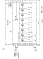
- FIGURE 1A is a simplified block diagram illustrating a system 10 comprising a trim circuit 12 to facilitate current source calibration tracking temperature and bias current.
- Trim circuit 12 can generate an output current that tracks and compensates for current mismatch between current sources 14(1) and a reference current source (not included in the figure) under varying environmental conditions.
- current source 14(1) may represent a current source under calibration, which can comprise a cascode device 14(2).
- Trim circuit 12 can include a current source 16 comprising an active electronic component (e.g., transistor).
- the gate voltage of current source 16 is not tied to the gate voltage of one of the external current sources (e.g., 14(1)).
- a bias circuit 18 generates the gate voltage of current source 16 such that the full scale current of trim circuit 12 is proportional to the product of transconductance (g m ) of current source 16 and an internally generated reference voltage V ref (e.g., g m (I, T)V ref ).
- V ref may be a constant factor of a bandgap voltage reference (e.g., temperature and load independent voltage, typically 1.25V).
- Each cell 20 of trim circuit 12 may include a portion of a current splitter and a switch configured according to SAR logic (or other suitable logic) to direct the current from current source 16 to either the drain of current source 14(1) (thereby increasing the output current of trim circuit 12) or discarded to a common return current node 22 (e.g., which may be common to substantially all calibration DACs in system 10).
- Cells 20 and current source 16 may collectively comprise a CAL DAC 24.
- a "CAL DAC” is any suitable digital to analog converter circuit that can be used to calibrate other circuits for various outputs (e.g., current mismatch between two current sources).
- each cell 20 can be switched on or off; current from each cell 20 is aggregated into the output current of trim circuit 12 when the cell is switched on, and current from the cell is diverted away from the output current of trim circuit 12 to return 22 when cell 20 is switched off.
- SAR logic may be used to configure each cell to be turned on or off. The on or off position of each cell 20 may be collectively saved to a digital value, called the 'CAL DAC value.' An output of CAL DAC 24 may be proportional to the CAL DAC value.
- trim circuit 12 may behave like a single DAC with its output current tracking transconductance (e.g., g m (I, T) ⁇ V TH ), which is proportional to bias current and temperature. As temperature T and/or bias current I changes, the current mismatch between current sources 14(1) and the reference current source may change. The output current of trim circuit 12 tracks the transconductance, which varies with temperature T and/or bias current I, and therefore the output current also changes accordingly. Thus, the output current can compensate for increased (or decreased) current mismatch between current sources 14(1) and the reference current source due to varying temperature and/or bias current.
- g m (I, T) ⁇ V TH output current tracking transconductance
- embodiments of system 10 include current source 14(1) with calibrated trim circuit 12, where an output current of trim circuit 12 varying with transconductance of current source 14(1) and tracking a current mismatch between current source 14(1) and another (e.g., reference) current source under varying bias currents and temperatures.
- trim circuit 12 comprises CAL DAC 24 whose output current changes with transconductance of current source 14(1) and tracks the current mismatch under varying bias currents and temperatures.
- the bias circuit 18 comprises a current generator generating current proportional to a bandgap voltage; two substantially identical resistors causing a voltage drop proportional to the current; and a differential transistor pair coupled to the current generator and the two resistors, where gate voltages of the differential transistor pair differ by twice the voltage drop, and an output current of the differential transistor pair (which is a difference between the drain current of the differential transistor pair) is proportional to the transconductance.
- the current generator may comprise an operational amplifier driving a voltage across a resistor to be a bandgap voltage, such that current across the resistor is proportional to the bandgap voltage.
- the resistor of the current generator may be substantially similar in type to the two resistors of bias circuit 18.
- bias circuit 18 may generate a gate voltage of current source 16 in trim circuit 12 that can cause a full scale current of CAL DAC 24 to be proportional to the transconductance.
- trim circuit 12 includes CAL DAC 24 connected to a current mirror, which may be connected to a drain of current source 14(1).
- the "current mirror” is a circuit configured to copy a current through one active device by controlling the current in another active device, keeping the output current constant regardless of loading.
- trim circuit 12 may include a voltage DAC connected to a gate of current source 16. The voltage DAC may comprise a plurality of resistors; the output of the voltage DAC may be based on an input digital code.
- trim circuit 12 may comprise a plurality of CAL DACs, where the output current of each CAL DAC changes with transconductance of the current source, where a sum of the output currents of the plurality of CAL DACs tracks the current mismatch under varying bias currents and temperatures.
- the output pins of the plurality of CAL DACs may be connected to a drain of current source 14(1).
- the plurality of CAL DACs may be connected to a drain of current source 14(1) through a current mirror.
- trim circuit 12 may comprise a plurality of CAL DACs, where a portion of the plurality of CAL DACs may provide output currents varying only with bias current; and a remaining portion of the plurality of CAL DACs may provide output currents varying with the transconductance of the current source (e.g., varying with both bias current and temperature), where a sum of the output currents of the plurality of CAL DACs tracks the current mismatch under varying bias currents and temperatures.
- trim circuit 12 comprises at least a first CAL DAC and a second CAL DAC, where a first output current of the first CAL DAC varies with bias current only, and a second output current of the second CAL DAC varies with bias current and temperature.
- the CAL DAC values of the first and second CAL DACs can be determined through multiple measurements under different bias currents and or temperature.
- a method for calibrating such a trim circuit comprises repeatedly varying calibration settings (e.g., settings of switches in the CAL DAC circuit, for example, that specifies whether the switch is turned on or off) of the first CAL DAC and the second CAL DAC under varying bias currents until an output current of the trim circuit substantially accurately tracks a current mismatch between two current sources under varying bias currents and temperatures.
- calibration settings e.g., settings of switches in the CAL DAC circuit, for example, that specifies whether the switch is turned on or off
- the method may include setting the second output current to zero, varying calibration settings of the first CAL DAC to force the output current of the trim circuit to match the current mismatch, changing bias current, holding calibration settings of the first CAL DAC at the previously set values while varying calibration settings of the second CAL DAC to force the output current of the trim circuit to match the current mismatch, and sequentially varying calibration settings of the first CAL DAC and the second CAL DAC at different bias currents until the output current of the trim circuit substantially accurately tracks the current mismatch under varying bias currents and temperatures.
- the method may further comprise changing the temperature substantially simultaneously with the bias current and varying calibration settings of the first CAL DAC and the second CAL DAC under varying temperatures until the output current of the trim circuit substantially accurately tracks the current mismatch between two current sources under varying bias currents and temperatures.
- SAR logic may be used to vary the calibration settings in some embodiments.
- FIGURE 1B is a simplified block diagram illustrating another embodiment of system 10, wherein transistors, including current source 14(1), cascode device 14(2) and current source 16 comprise PMOS transistors.
- the operations of trim circuit 12 according to the embodiment are virtually identical when the transistors comprise NMOS transistors, as illustrated in the previous FIGURE 1A .
- FIGURE 2 is a simplified block diagram illustrating example details of trim circuit 12 according to another embodiment of system 10.
- Trim circuit 12 includes CAL DAC 24 (e.g., comprising switches and trim circuits that can be turned on according to SAR logic).
- CAL DAC 24 may be driven by a bias circuit (not shown) which can generate current proportional to transconductance (e.g., g m V ref ) of current source 14(1).
- a bias circuit not shown
- Trim circuit 12 also includes a current mirror 26.
- Current mirror 26 is not limited to the simple circuit shown in the figure and can be any type of current mirror according to the broad scope of the embodiments.
- the CAL DAC value of CAL DAC 24 can be determined through generally known methods to be a suitable fraction of the full scale current.
- the transistors of current mirror 26 can be configured (e.g., designed) to affect the current output from current source 16 within CAL DAC 24, for example, based on the CAL DAC value.
- FIGURE 3 is a simplified block diagram illustrating example details of trim circuit 12 according to another embodiment of system 10.
- Trim circuit 12 can include a plurality of CAL DACs 24(1)-24(N), with each CAL DAC having a different environmental dependence.
- CAL DAC 24(1) may be driven by a bias circuit (not shown) which can generate current proportional to transconductance (e.g., g m V ref ) of current source 14(1).
- the full scale output current of CAL DAC 24(1) may be proportional to transconductance.
- output current of CAL DAC 24(2) may also vary with transconductance.
- output current of CAL DAC 24(2) may vary only with bias current.
- Various other environmental dependencies may be included within the broad scope of the embodiments.
- FIGURE 4 is a simplified block diagram illustrating example details of trim circuit 12 according to another embodiment of system 10.
- Trim circuit 12 can include two CAL DACs 24(1) and 24(2), and current mirror 26.
- the full scale current of CAL DAC 24(1) may be proportional to bias current I , for example, to track ⁇ ⁇ I
- the full scale current of CAL DAC 24(2) may be proportional to g m V ref , for example, to track g m ⁇ V TH .
- CAL DAC 24(2) may be driven by bias circuit 18 (not shown) that generates current proportional to the transconductance.
- Current mirror 26 may feed a sum of output currents of CAL DACs 24(1) and 24(2) to current source 16.
- Current mirror 26 is not limited to the simple circuit shown in the figure and can be any type of current mirror according to the broad scope of the embodiments.
- FIGURE 5 is a simplified block diagram illustrating example details of a current generator 28 according to an embodiment of system 10.
- V BC is the bandgap voltage generated by external circuitry (not shown).
- Voltage across resistor 32 (whose resistance is R I ) is fixed to V BC by op amp 30. Therefore, I R , current through resistor 32, is V BG / R I .
- I R current through resistor 32
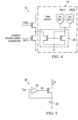
- FIGURE 6 is a simplified block diagram illustrating a circuit 36 configured to generate output current proportional to g m V ref according to an embodiment of system 10.
- Current generator 28 generating current I R can be copied by a current mirror suitably, with a bias voltage V b applied between the two current generators 28.
- Resistors 38(1) and 38(2) may comprise a same type of resistor, having resistance R.
- resistors 38(1) and 38(2) may comprise the same type of resistor as resistor 32, which is used in current generator 28.
- a ratio of resistances, namely R / R I may be invariant with temperature and a constant in various environments.
- a differential transistor pair comprising transistors 40(1) and 40(2), along with an appropriate current mirror biasing stage 42 may be included in circuit 36.
- the differential transistor pair with its current-mirror biasing stage may be made from matched-pair devices to minimize imbalances from one side of the differential transistor pair to the other.
- the gate voltages of differential transistor pair 40(1) and 40(2) may be V b - I R R and V b + I R R, respectively, where V b is the bias voltage.
- the output current which may be accessed at current mirror 42, is a difference between the drain current of the differential pair 40(1) and 40(2).
- the difference in drain current is g m V ref , where g m is the transconductance of transistor 40(1).
- FIGURE 7 is a simplified block diagram illustrating details of an example bias circuit 18 according to an embodiment of system 10.
- Circuit 36 configured to generate output current proportional to g m V ref may be connected to a diode 44 to generate a voltage (e.g., V cal ) that can force the output current of CAL DAC 24 to be proportional to transconductance and V ref (e.g., g m V ref ).
- V cal a voltage
- V ref e.g., g m V ref
- a body diode comprising a MOSFET is used for diode 44 in the figure; however, any suitable generic diode or other component that blocks current in one direction can be used within the broad scope of the embodiments.
- Current generator 28 may be included in circuit 36 with appropriate current mirrors 42 and other transistors suitably to supply current I R to differential transistor pair 40(1) and 40(2). Note that current proportional to g m V ref flows out of bias circuit 18 according to the example embodiment shown herein. Various other combinations of components can also be used to achieve the functionalities described herein within the broad scope of the embodiments.
- FIGURE 8 is a simplified block diagram illustrating details of another example bias circuit 18 according to another embodiment of system 10.
- Circuit 36 configured to generate output current proportional to g m V ref may be connected to a diode 44 to generate a voltage (e.g., V cal ) that can force the output current of trim circuit 12 to be proportional to transconductance and V ref (e.g., g m V ref ), for example, when CAL DAC 24 is connected to current source 16 within trim circuit 12, and the output therefrom is directly connected to the drain of current source 14(1).
- a body diode comprising a MOSFET is used for diode 44 in the figure; however, any suitable generic diode or other component that blocks current in one direction can be used within the broad scope of the embodiments.
- Current generator 28 may be included in circuit 36 with appropriate current mirrors 42 and other transistors suitably to supply current I R to differential transistor pair 40(1) and 40(2). Note that the gate voltages of transistors 40(1) and 40(2) are swapped when compared to the embodiment described with reference to the previous figure. Note that current proportional to g m V ref flows into bias circuit 18 according to the example embodiment shown herein. Various other combinations of components can also be used to achieve the functionalities described herein within the broad scope of the embodiments.
- FIGURE 9 is a simplified diagram illustrating an example CAL DAC 24 (and other details) according to an embodiment of system 10.
- Trim circuit 12 may comprise a voltage DAC 48 driven by current generator 28.
- the gate of transistor 16 may be connected to voltage DAC 48 whose output is a voltage based on a digital input.
- Voltage DAC 48 may comprise a resistor string including switches 50 and resistors 52. Current generated by current generator 28 flowing through the resistor string may generates different voltages at each internal resistor's nodes. Therefore the voltage drop across the resistors may be proportional to the bandgap voltage ( V ref ) and may be constant.
- a digital input may control switch 50, select a voltage and output the voltage (proportional to V ref ) .
- the current of transistor 16 may be g m V voltage DAC .
- g m (where g m is transconductance of transistor 16, and V voltageDAC is the output voltage of voltage DAC 48) is designed to be proportional to gm of current source 14(1); thus trim circuit may generate a current proportional to g m V ref .
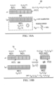
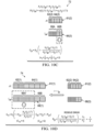
- FIGURES 10A-10D are simplified diagrams illustrating certain operational details of calibrating trim circuit 12 according to an embodiment of system 10. If m CAL DAC values are to be determined, at least m data points may be required. At least m measurements may be performed under m different environments such as different temperature or bias current to obtain at least m data points. Changing temperature can be time consuming, costly and probably impractical for production test. Changing bias currents is more preferable for testing. Thus, the m CAL DAC values can be extracted from the m measurements.
- trim circuit 12 comprises at least two CAL DACs 24(1) and 24(2).
- the output current of CAL DAC 24(1) varies with the bias current I
- the output current of CAL DAC 24(2) varies with g m V ref (and thus varies with both temperature and bias current).
- a unit current of CAL DAC 24(1) is U 1 ⁇ I
- a unit current of CAL DAC 24(2) is U 2 ⁇ g m V ref .
- ⁇ I I T ⁇ ⁇ I ⁇ g m I T ⁇ V TH , where ⁇ ⁇ I is 1.2uA and -g m (I, T) ⁇ V TH is 2uA.
- C 20 is set to be 0 and only CAL DAC 24(1) is calibrated to generate an output current equal to a target current mismatch.
- C 20 is set to 0 merely for convenience; C 20 can be set to any suitable value based on particular needs.
- An example embodiment may implement SAR logic as a possible way for measurement.
- R 20 is 100% after the initial cycle.
- CAL DAC 24(1)'s contribution to current mismatch ⁇ I 61(1) between current sources 14(1) and 14(2) is denoted as current contribution 62(1) and CAL DAC 24(2)'s contribution to current mismatch ⁇ I is denoted as current contribution 64(1).
- the output current of trim circuit 12 may be denoted as I cal 66(1).
- I cal 66(1) would be equal to current mismatch ⁇ I 61(1), and when both CAL DAC 24(1) and CAL DAC 24(2) are calibrated appropriately to varying bias current and temperature, I cal 66(1) may include appropriate contributions from CAL DAC 24(1) and CAL DAC 24(2).
- the CAL DAC value of CAL DAC 24(1) namely, C 10
- the CAL DAC value of CAL DAC 24(1) may be set (e.g., configured, determined, established, estimated, approximated, etc., based on SAR logic or other suitable logic) to obtain I cal 66(1) while holding the output current of CAL DAC 24(2) (C 20 ) at 0.
- the current source bias current may change from I to I m and the temperature may be kept constant or ignored (e.g., temperature can vary without affecting the results).
- U 1 ( I ) and U 2 ( I , T ) can change differently (e.g., because of their different dependencies on bias current).
- CAL DAC 24(1)'s contribution to current mismatch ⁇ I 61(2) between current sources 14(1) and 14(2) may be changed to current contribution 62(2) and CAL DAC 24(2)'s contribution to current mismatch ⁇ I 61(2) may be changed to current contribution 64(2);
- I cal 66(2) may also be reduced to C 10 U 1 ( I M ) and the may no longer be equal to I cal 66(1).
- CAL DAC value of CAL DAC 24(1) may be held to be C 10 .
- contribution of CAL DAC 24(1) to I cal 66(3) may be indicated as 66A, and may remain equal to I cal 66(2) from previous step 70.
- Only CAL DAC 24(2) may be used in the calibration measurement to force I cal 66(3) to equal current mismatch ⁇ I 61(2).
- CAL DAC value of CAL DAC 24(2) may be determined through SAR logic (or other suitable logic) to get an output current 66B, which when added to 66A, results in I cal 66(3) being equal to current mismatch ⁇ I 61(2).
- next step 74 as shown in Figure 10D , the current source current may be restored to I .
- current mismatch ⁇ I 61(2) may revert back to current mismatch ⁇ I 61(1);
- CAL DAC 24(1)'s contribution to current mismatch ⁇ I 61(1) may revert back to current contribution 62(1);
- CAL DAC 24(2)'s contribution to current mismatch ⁇ I 61(1) may revert back to current contribution 64(1).
- CAL DAC value of CAL DAC 24(2) may be held to be C 21 , thereby fixing contribution of CAL DAC 24(2) to I cal 66(1) at 66B, from previous step 72.
- Configuration settings of CAL DAC 24(1) may be changed appropriately to obtain a CAL DAC value of 66A', which when added to 66B, results in I cal 66(1) being equal to current mismatch ⁇ I 61(1).
- R 21 is reduced and C 11 and C 21 are closer to X 1 and X 2 .
- CAL DAC 24(1) and CAL DAC 24(2) may be swapped in all steps.
- the bias current I may be held at a constant value and only temperature T may be changed.
- both bias current and temperature may be changes substantially simultaneously.
- FIGURE 11 is a simplified flow diagram illustrating example operations 100 that may be associated with a calibration method according to embodiments of system 10.
- trim circuit 12 comprises at least two CAL DACs 24(1) and 24(2).
- the output current of CAL DAC 24(1) varies with the bias current I
- the output current of CAL DAC 24(2) varies with g m V ref (and thus varies with both temperature and bias current).
- the operations may start at 102.
- the CAL DAC value of CAL DAC 24(2) may be set to zero.
- the CAL DAC value of CAL DAC 24(1) may be determined (e.g., according to SAR logic, or other suitable logic) to force trim circuit output current ( I cal ) to equal current mismatch ( ⁇ I ) between current sources 14(1) and 14(2).
- current source bias current (and/or temperature in some embodiments) may be changed.
- the CAL DAC value of CAL DAC 24(1) may be held at the previously determined value (at 106).
- the CAL DAC value of CAL DAC 24(2) may be determined (e.g., according to SAR logic, or other suitable logic) to force trim circuit output current ( I cal ) to equal current mismatch ( ⁇ I ) between current sources 14(1) and 14(2).
- the current source bias current (and/or temperature) may be restored to original values.
- the CAL DAC value of CAL DAC 24(2) may be held at the previously determined value (at 112).
- the CAL DAC value of CAL DAC 24(1) may be determined (e.g., according to SAR logic, or other suitable logic) to force trim circuit output current ( I ca / ) to equal current mismatch ( ⁇ I ) between current sources 14(1) and 14(2).
- the bias current (and/or temperature) may be changed.
- a determination may be made at 122 if a predetermined number of iterations is over. If the predetermined number of iterations is over, the operations may end at 124. Otherwise, the operations may loop back to 110, and continue thereafter.
- references to various features e.g., elements, structures, modules, components, steps, operations, characteristics, etc.
- references to various features e.g., elements, structures, modules, components, steps, operations, characteristics, etc.
- references to various features are intended to mean that any such features are included in one or more embodiments of the present disclosure, but may or may not necessarily be combined in the same embodiments.
- capacitors, clocks, DFFs, dividers, inductors, resistors, amplifiers, switches, digital core, transistors, and/or other components can readily be replaced, substituted, or otherwise modified in order to accommodate particular circuitry needs.
- the use of complementary electronic chips, hardware, software, etc. offer an equally viable option for implementing the teachings of the present disclosure.
- any number of electrical circuits of the FIGURES may be implemented on a board of an associated electronic chip.
- the board can be a general circuit board that can hold various components of the internal electronic system of the electronic chip and, further, provide connectors for other peripherals. More specifically, the board can provide the electrical connections by which the other components of the system can communicate electrically.
- Any suitable processors (inclusive of digital signal processors, microprocessors, supporting chipsets, etc.), memory elements, etc. can be suitably coupled to the board based on particular configuration needs, processing demands, computer designs, etc.
- Other components such as external storage, additional sensors, controllers for audio/video display, and other peripheral chips may be attached to the board as plug-in cards, via cables, or integrated into the board itself.
- the electrical circuits of the FIGURES may be implemented as stand-alone modules (e.g., a chip with associated components and circuitry configured to perform a specific application or function) or implemented as plug-in modules into application specific hardware of electronic chips.
- stand-alone modules e.g., a chip with associated components and circuitry configured to perform a specific application or function
- plug-in modules into application specific hardware of electronic chips.
- SOC system on chip
- An SOC represents an IC that integrates components of a computer or other electronic system into a single chip. It may contain digital, analog, mixed-signal, and often radio frequency functions: all of which may be provided on a single chip substrate.
- MCM multi-chip-module
- ASICs Application Specific Integrated Circuits
- FPGAs Field Programmable Gate Arrays
- the activities discussed above with reference to the FIGURES are applicable to any integrated circuits that involve signal processing, particularly those that rely on synchronization signals to execute specialized software programs, or algorithms, some of which may be associated with processing digitized real-time data.
- Certain embodiments can relate to multi-DSP signal processing, floating point processing, signal/control processing, fixed-function processing, microcontroller applications, etc.
- the features discussed herein can be applicable to medical systems, scientific instrumentation, wireless and wired communications, radar, industrial process control, audio and video equipment, current sensing, instrumentation (which can be highly precise), and other digital-processing-based systems.
- certain embodiments discussed above can be provisioned in digital signal processing technologies for medical imaging, patient monitoring, medical instrumentation, and home healthcare. This could include pulmonary monitors, accelerometers, heart rate monitors, pacemakers, etc. Other applications can involve automotive technologies for safety systems (e.g., stability control systems, driver assistance systems, braking systems, infotainment and interior applications of any kind). Furthermore, powertrain systems (for example, in hybrid and electric vehicles) can apply the functionalities described herein in high-precision data conversion products in battery monitoring, control systems, reporting controls, maintenance activities, etc.
- the teachings of the present disclosure can be applicable in the industrial markets that include process control systems that help drive productivity, energy efficiency, and reliability.
- the teachings of the electrical circuits discussed above can be used for image processing, auto focus, and image stabilization (e.g., for digital still cameras, camcorders, etc.).
- Other consumer applications can include audio and video processors for home theater systems, DVD recorders, and high-definition televisions.
- Yet other consumer applications can involve advanced touch screen controllers (e.g., for any type of portable media chip).
- such technologies could readily part of smartphones, tablets, security systems, PCs, gaming technologies, virtual reality, simulation training, etc.
- a system that can include any suitable circuitry, dividers, capacitors, resistors, inductors, ADCs, DFFs, logic gates, software, hardware, links, etc.
- any suitable circuitry e.g., dividers, capacitors, resistors, inductors, ADCs, DFFs, logic gates, software, hardware, links, etc.
- ADCs analog to digital converters
- DFFs digital to analog converters
- logic gates software, hardware, links, etc.
- the system can include means for calibrating a trim circuit comprising at least a first CAL DAC and a second CAL DAC, including means for varying calibration settings of the first CAL DAC and the second CAL DAC under varying bias currents until an output current of the trim circuit substantially accurately tracks a current mismatch between two current sources under varying bias currents and temperatures, wherein a first output current of the first CAL DAC varies with bias current only, and a second output current of the second CAL DAC varies with bias current and temperature, wherein the output current of the trim circuit is a sum of the first output current and the second output current.
- the system can also include means for setting the second output current to zero; means for varying calibration settings of the first CAL DAC to force the output current of the trim circuit to match the current mismatch; means for changing bias current; means for holding calibration settings of the first CAL DAC at the previously set values while varying calibration settings of the second CAL DAC to force the output current of the trim circuit to match the current mismatch; and means for sequentially varying calibration settings of the first CAL DAC and the second CAL DAC at different bias currents until the output current of the trim circuit substantially accurately tracks the current mismatch under varying bias currents and temperatures.
- the system can also include means for changing the temperature substantially simultaneously with the bias current; and means for varying calibration settings of the first CAL DAC and the second CAL DAC under varying temperatures until the output current of the trim circuit substantially accurately tracks the current mismatch between two current sources under varying bias currents and temperatures.
- the 'means for' in these instances can include (but is not limited to) using any suitable component discussed herein, along with any suitable software, circuitry, hub, computer code, logic, algorithms, hardware, controller, interface, link, bus, communication pathway, etc.
- the system includes memory that further comprises machine-readable instructions that when executed cause the system to perform any of the activities discussed above.
Landscapes
- Engineering & Computer Science (AREA)
- Theoretical Computer Science (AREA)
- Physics & Mathematics (AREA)
- Electromagnetism (AREA)
- General Physics & Mathematics (AREA)
- Radar, Positioning & Navigation (AREA)
- Automation & Control Theory (AREA)
- Power Engineering (AREA)
- Amplifiers (AREA)
- Control Of Electrical Variables (AREA)
- Semiconductor Integrated Circuits (AREA)
Claims (10)
- Schaltung, die konfiguriert ist, eine Änderung der Stromfehlanpassung zwischen einer ersten Stromquelle und einer Bezugsstromquelle unter verschiedenen Temperaturen zu verfolgen, wobei die Schaltung Folgendes umfasst:die erste Stromquelle (14(1)), wobei die erste Stromquelle einen ersten Transistor umfasst, der eine erste Transkonduktanz aufweist, die mit der Temperatur variiert, und die erste Stromquelle durch eine erste Vorspannung angesteuert wird, undeine Abgleichschaltung (12), die an die erste Stromquelle gekoppelt ist, um einen Ausgangsstrom zum Kalibrieren der ersten Stromquelle zur ersten Stromquelle zu liefern, wobei die Abgleichschaltung Folgendes umfasst:eine Vorspannungsschaltung (18), die konfiguriert ist, einen Vorspannungsstrom zu erzeugen, der mit der Temperatur variiert, wobei die Vorspannungsschaltung ein Differenzialtransistorpaar, das eine zweite Transkonduktanz aufweist, die mit der Temperatur variiert, umfasst, die Schwankung der zweiten Transkonduktanz mit der Temperatur proportional zur Schwankung der ersten Transkonduktanz mit der Temperatur ist und der Vorspannungsstrom eine Differenz zwischen den Drain-Strömen des Differenzialtransistorpaars ist und zur zweiten Transkonduktanz des Differenzialtransistorpaars proportional ist, wobei die Vorspannungsschaltung ferner einen Stromgenerator, der einen Strom erzeugt, der zu einer Bandlückenspannung proportional ist, und zwei im Wesentlichen identische Widerstände, die einen zum Strom proportionalen Spannungsabfall verursachen, umfasst, das Differenzialtransistorpaar an den Stromgenerator und die zwei Widerstände gekoppelt ist und Gate-Spannungen des Differenzialtransistorpaars sich um das Zweifache des Spannungsabfalls unterscheiden; undeinen Kalibrierungs-Digital/Analog-Umsetzer, CAL DAC (24), der konfiguriert ist, den Ausgangsstrom der Abgleichschaltung zu setzen, wobei eine zweite Vorspannung des CAL DAC unabhängig von der ersten Vorspannung ist und aus dem Vorspannungsstrom hergeleitet wird, derart, dass der Ausgangsstrom der Abgleichschaltung mit der Temperatur variiert, um die Änderung der Stromfehlanpassung zwischen der ersten Stromquelle und der Bezugsstromquelle unter verschiedenen Temperaturen zu verfolgen.
- Schaltung nach Anspruch 1, wobei der Stromgenerator einen Operationsverstärker umfasst, der eine Spannung über einem dritten Widerstand derart ansteuert, dass sie eine Bandlückenspannung ist, wobei der Strom durch den dritten Widerstand zur Bandlückenspannung proportional ist und der dritte Widerstand einen Temperaturkoeffizienten aufweist, der zu jenem der zwei im Wesentlichen identischen Widerstände im Wesentlichen ähnlich ist.
- Schaltung nach Anspruch 1 oder 2, wobei der CAL DAC mehrere Zellen zum Leiten des Vorspannungsstroms in den Ausgangsstrom oder weg vom Ausgangsstrom umfasst, wobei jede Zelle ein- oder ausgeschaltet werden kann, der Vorspannungsstrom durch eine Zelle geleitet wird, um in den Ausgangsstrom der Abgleichschaltung zusammengefasst zu werden, wenn die Zelle eingeschaltet ist, und Strom aus einer Zelle vom Ausgangsstrom der Abgleichschaltung weg umgeleitet wird, wenn die Zelle ausgeschaltet ist.
- Schaltung nach einem vorhergehenden Anspruch, wobei die Abgleichschaltung einen Stromspiegel (26) enthält und der Stromspiegel mit einem Drain der ersten Stromquelle und einem Ausgang des CAL DAC verbunden ist.
- Schaltung nach einem vorhergehenden Anspruch, wobei die Abgleichschaltung ferner eine zweite Stromquelle (16) umfasst, die zweite Vorspannung an eine Gate-Spannung der zweiten Stromquelle angelegt ist und die Gate-Spannung der zweiten Stromquelle verursacht, dass ein vollausgesteuerter Strom zum CAL DAC mit der Temperatur variiert.
- Schaltung nach einem vorhergehenden Anspruch, wobei der Ausgangsstrom der Abgleichschaltung die Stromfehlanpassung zwischen der ersten Stromquelle und der Bezugsstromquelle unter verschiedenen Vorspannungsströmen verfolgt.
- Schaltung nach einem vorhergehenden Anspruch, wobeidie Abgleichschaltung mehrere CAL DACs umfasst,der Ausgangsstrom jedes CAL DAC sich mit der Temperatur ändert undeine Summe der Ausgangsströme der mehreren CAL DACs die Stromfehlanpassung zwischen der ersten Stromquelle und der Bezugsstromquelle unter verschiedenen Vorspannungsströmen und Temperaturen verfolgt.
- Schaltung nach einem der Ansprüche 1 bis 6, wobeidie Abgleichschaltung einen weiteren CAL DAC umfasst undein Ausgangsstrom des weiteren CAL DAC lediglich mit dem Vorspannungsstrom variiert und ein Ausgangsstrom des CAL DAC mit dem Vorspannungsstrom und der Temperatur variiert.
- Schaltung nach Anspruch 7 oder Anspruch 8, wobei Ausgangskontakte der mehreren CAL DACs, die die Ausgangsströme der mehreren CAL DACs ausgeben, mit einem Drain der ersten Stromquelle verbunden sind.
- Schaltung nach einem der Ansprüche 7 bis 9, wobei Ausgangskontakte der mehreren CAL DACs, die die Ausgangsströme der mehreren CAL DACs ausgeben, durch einen Stromspiegel (26) mit einem Drain der ersten Stromquelle verbunden sind.
Applications Claiming Priority (2)
| Application Number | Priority Date | Filing Date | Title |
|---|---|---|---|
| US14/169,986 US10048714B2 (en) | 2014-01-31 | 2014-01-31 | Current source calibration tracking temperature and bias current |
| EP15151969.1A EP2911301A1 (de) | 2014-01-31 | 2015-01-21 | Stromquellenkalibrierung mit Verfolgung von Temperatur und Vorspannungsstrom |
Related Parent Applications (1)
| Application Number | Title | Priority Date | Filing Date |
|---|---|---|---|
| EP15151969.1A Division EP2911301A1 (de) | 2014-01-31 | 2015-01-21 | Stromquellenkalibrierung mit Verfolgung von Temperatur und Vorspannungsstrom |
Publications (2)
| Publication Number | Publication Date |
|---|---|
| EP3484052A1 EP3484052A1 (de) | 2019-05-15 |
| EP3484052B1 true EP3484052B1 (de) | 2024-09-04 |
Family
ID=52354878
Family Applications (2)
| Application Number | Title | Priority Date | Filing Date |
|---|---|---|---|
| EP18211740.8A Active EP3484052B1 (de) | 2014-01-31 | 2015-01-21 | Stromquellenkalibrierung mit verfolgung von temperatur und vorspannungsstrom |
| EP15151969.1A Withdrawn EP2911301A1 (de) | 2014-01-31 | 2015-01-21 | Stromquellenkalibrierung mit Verfolgung von Temperatur und Vorspannungsstrom |
Family Applications After (1)
| Application Number | Title | Priority Date | Filing Date |
|---|---|---|---|
| EP15151969.1A Withdrawn EP2911301A1 (de) | 2014-01-31 | 2015-01-21 | Stromquellenkalibrierung mit Verfolgung von Temperatur und Vorspannungsstrom |
Country Status (3)
| Country | Link |
|---|---|
| US (2) | US10048714B2 (de) |
| EP (2) | EP3484052B1 (de) |
| CN (1) | CN104820456B (de) |
Families Citing this family (21)
| Publication number | Priority date | Publication date | Assignee | Title |
|---|---|---|---|---|
| US8633873B2 (en) * | 2009-11-12 | 2014-01-21 | Ignis Innovation Inc. | Stable fast programming scheme for displays |
| CN104183353B (zh) * | 2013-05-28 | 2016-12-28 | 北京北方微电子基地设备工艺研究中心有限责任公司 | 电磁铁线圈组件、半导体加工设备及其控制方法 |
| CN108702158B (zh) * | 2016-02-25 | 2022-04-05 | ams有限公司 | 数模转换器和数模转换方法 |
| US10038431B1 (en) * | 2017-06-01 | 2018-07-31 | Nuvoton Technology Corporation | Current mirror array for high-frequency clock generator |
| CN107124148B (zh) * | 2017-06-08 | 2024-06-28 | 尚睿微电子(上海)有限公司 | 一种控制电路、偏置电路及控制方法 |
| US10305361B2 (en) | 2017-06-09 | 2019-05-28 | Qualcomm Incorporated | Low voltage input calibrating digital to analog converter |
| US10333497B1 (en) * | 2018-04-04 | 2019-06-25 | Globalfoundries Inc. | Calibration devices for I/O driver circuits having switches biased differently for different temperatures |
| US10345841B1 (en) * | 2018-06-12 | 2019-07-09 | Nxp Usa, Inc. | Current source with variable resistor circuit |
| CN111065187B (zh) * | 2018-10-17 | 2022-04-26 | 戴洛格半导体(英国)有限公司 | 电流调节器 |
| US10819365B1 (en) * | 2020-02-06 | 2020-10-27 | Analog Devices, Inc. | Utilizing current memory property in current steering digital-to-analog converters |
| TWI719891B (zh) * | 2020-04-22 | 2021-02-21 | 瑞昱半導體股份有限公司 | 偏壓補償裝置及操作偏壓補償裝置的方法 |
| CN113568464B (zh) * | 2020-04-29 | 2023-03-28 | 瑞昱半导体股份有限公司 | 偏压补偿装置及操作偏压补偿装置的方法 |
| CN111800140A (zh) * | 2020-06-22 | 2020-10-20 | 复旦大学 | 一种应用于柔性材料的具有校正功能的8位数模转换器 |
| FR3113777B1 (fr) * | 2020-08-25 | 2024-12-13 | St Microelectronics Rousset | Alimentation de circuit électronique |
| CN116075730A (zh) * | 2020-09-08 | 2023-05-05 | 美国亚德诺半导体公司 | 电池内部温度的估计技术 |
| US11469876B1 (en) * | 2020-09-25 | 2022-10-11 | Raytheon Company | Trigger to data synchronization of gigahertz digital-to-analog converters |
| CN114415770B (zh) * | 2021-12-22 | 2023-11-14 | 深圳航天科技创新研究院 | 用于磁共振设备的匀场电流源装置 |
| CN114911298A (zh) * | 2022-04-28 | 2022-08-16 | 北京集创北方科技股份有限公司 | 过温保护电路及其测试方法 |
| CN114740942A (zh) * | 2022-05-24 | 2022-07-12 | 北京芯通未来科技发展有限公司 | 电流校准电路 |
| CN115494908B (zh) * | 2022-10-17 | 2023-11-17 | 中国电子科技集团公司第二十四研究所 | 跟踪温度的电流源失配前台校准电路及方法 |
| CN121036700B (zh) * | 2025-08-15 | 2026-03-20 | 沈阳工业大学 | 一种多温度系数偏置系统 |
Citations (4)
| Publication number | Priority date | Publication date | Assignee | Title |
|---|---|---|---|---|
| EP0561099B1 (de) * | 1992-03-20 | 1995-09-06 | STMicroelectronics S.r.l. | Schaltungsanordnung zur Abhängigkeitsunterdrückung vom Temperatur und von Herstellungsvariabelen der Steilheit einer differentiellen Transkonduktanzstufe |
| EP0766385B1 (de) * | 1995-09-29 | 2003-03-26 | Harris Corporation | Aktive Vorspannungssteuerung für zeitkontinuierliche integrierte Schaltung |
| EP0818884B1 (de) * | 1996-07-12 | 2004-03-31 | Samsung Electronics Co., Ltd. | Einrichtung zur Stabilisierung der Grenzfrequenz unter Benutzung einer Transkonduktanz |
| US20050073290A1 (en) * | 2003-10-07 | 2005-04-07 | Stefan Marinca | Method and apparatus for compensating for temperature drift in semiconductor processes and circuitry |
Family Cites Families (12)
| Publication number | Priority date | Publication date | Assignee | Title |
|---|---|---|---|---|
| WO1994017590A1 (en) * | 1993-01-27 | 1994-08-04 | Micro Linear Corporation | Circuit technique that sets transconductance |
| US6822505B1 (en) | 1999-12-27 | 2004-11-23 | Texas Instruments Incorporated | Mobility compensation in MOS integrated circuits |
| US6459293B1 (en) | 2000-09-29 | 2002-10-01 | Intel Corporation | Multiple parameter testing with improved sensitivity |
| US6507296B1 (en) * | 2001-08-14 | 2003-01-14 | Xilinx, Inc. | Current source calibration circuit |
| US6583740B2 (en) | 2001-11-21 | 2003-06-24 | Analog Devices, Inc. | Calibrated current source |
| KR100588339B1 (ko) | 2004-01-07 | 2006-06-09 | 삼성전자주식회사 | 오토 튜닝 기능을 갖는 전압-전류 변환회로를 구비한전류원 회로 |
| KR100664305B1 (ko) * | 2005-02-04 | 2007-01-04 | 삼성전자주식회사 | 전류모드 트랜스컨덕터 튜닝 장치 |
| US7443323B2 (en) * | 2007-01-10 | 2008-10-28 | Freescale Semiconductor, Inc. | Calibrating a digital-to-analog converter |
| JP4960216B2 (ja) * | 2007-12-28 | 2012-06-27 | ルネサスエレクトロニクス株式会社 | D/a変換回路 |
| US8031098B1 (en) * | 2010-01-19 | 2011-10-04 | National Semiconductor Corporation | DAC circuit with pseudo-return-to-zero scheme and DAC calibration circuit and method |
| US9275187B2 (en) | 2011-03-21 | 2016-03-01 | Ridgetop Group, Inc. | Programmable test chip, system and method for characterization of integrated circuit fabrication processes |
| US8576101B1 (en) * | 2012-11-05 | 2013-11-05 | Google Inc. | Calibration of an R2R ladder based current digital-to-analog converter (DAC) |
-
2014
- 2014-01-31 US US14/169,986 patent/US10048714B2/en active Active
-
2015
- 2015-01-21 EP EP18211740.8A patent/EP3484052B1/de active Active
- 2015-01-21 EP EP15151969.1A patent/EP2911301A1/de not_active Withdrawn
- 2015-01-30 CN CN201510048292.0A patent/CN104820456B/zh active Active
-
2018
- 2018-08-13 US US16/102,637 patent/US10579086B2/en active Active
Patent Citations (4)
| Publication number | Priority date | Publication date | Assignee | Title |
|---|---|---|---|---|
| EP0561099B1 (de) * | 1992-03-20 | 1995-09-06 | STMicroelectronics S.r.l. | Schaltungsanordnung zur Abhängigkeitsunterdrückung vom Temperatur und von Herstellungsvariabelen der Steilheit einer differentiellen Transkonduktanzstufe |
| EP0766385B1 (de) * | 1995-09-29 | 2003-03-26 | Harris Corporation | Aktive Vorspannungssteuerung für zeitkontinuierliche integrierte Schaltung |
| EP0818884B1 (de) * | 1996-07-12 | 2004-03-31 | Samsung Electronics Co., Ltd. | Einrichtung zur Stabilisierung der Grenzfrequenz unter Benutzung einer Transkonduktanz |
| US20050073290A1 (en) * | 2003-10-07 | 2005-04-07 | Stefan Marinca | Method and apparatus for compensating for temperature drift in semiconductor processes and circuitry |
Non-Patent Citations (1)
| Title |
|---|
| CHAO SU ET AL: "Dynamic calibration of current-steering DAC", 2006 IEEE INTERNATIONAL SYMPOSIUM ON CIRCUITS AND SYSTEMS 21-24 MAY 2006 ISLAND OF KOS, GREECE, IEEE - PISCATAWAY, NJ, USA, 21 May 2006 (2006-05-21), pages 4pp - 120, XP032457659, ISBN: 978-0-7803-9389-9, DOI: 10.1109/ISCAS.2006.1692536 * |
Also Published As
| Publication number | Publication date |
|---|---|
| US20180348806A1 (en) | 2018-12-06 |
| US10579086B2 (en) | 2020-03-03 |
| CN104820456B (zh) | 2018-01-12 |
| US20150220100A1 (en) | 2015-08-06 |
| EP3484052A1 (de) | 2019-05-15 |
| CN104820456A (zh) | 2015-08-05 |
| EP2911301A1 (de) | 2015-08-26 |
| US10048714B2 (en) | 2018-08-14 |
Similar Documents
| Publication | Publication Date | Title |
|---|---|---|
| US10579086B2 (en) | Current source calibration tracking temperature and bias current | |
| US10637495B2 (en) | SAR ADCs with dedicated reference capacitor for each bit capacitor | |
| US10148278B2 (en) | Sigma-delta analog-to-digital converter including loop filter having components for feedback digital-to-analog converter correction | |
| EP2779462B1 (de) | Taktsignalfehlerkorrektur in einem Digital/Analog-Umsetzer | |
| US9970825B2 (en) | Temperature sensing with feedback digital-analog converter (DAC) of delta-sigma modulator | |
| US8536844B1 (en) | Self-calibrating, stable LDO regulator | |
| US11563442B2 (en) | Calibration of continuous-time residue generation systems for analog-to-digital converters | |
| EP3402079B1 (de) | Analog-digital-umsetzer, messanordnung und verfahren zur analog-digital-umsetzung | |
| CN108871633A (zh) | 压力传感器的信号调理电路 | |
| CN114079462A (zh) | 具有自动归零残余放大电路的模数转换器 | |
| US9397682B2 (en) | Reference buffer with wide trim range | |
| US11057047B2 (en) | Ratiometric gain error calibration schemes for delta-sigma ADCs with capacitive gain input stages | |
| EP3070485B1 (de) | Begrenzung von alterungsauswirkungen in analogen differenzschaltungen | |
| US20190227586A1 (en) | Resistance calibration | |
| CN115420334B (zh) | 监测装置、电子设备和监测方法 | |
| US9444405B1 (en) | Methods and structures for dynamically reducing DC offset | |
| EP1632779B1 (de) | Hall-Sensor-Modul und integrierte Schaltung zur Benutzung mit einem externen Hall-Sensor | |
| US9768794B1 (en) | Analog-to-digital converter having a switched capacitor circuit | |
| US20250080064A1 (en) | Method, device and apparatus for biasing a power amplifier operative over wide supply range | |
| CN118444740A (zh) | 温漂校准电路、芯片及电子设备 | |
| Nankoo et al. | A digitally-assisted error compensation grouping method for element matching improvement in data converters | |
| JP2025125450A (ja) | オフセット調整システムおよびオフセット調整装置 | |
| CN120675508A (zh) | 用于具有由输出负载设置的增益的高准确性开环跨导放大器的系统和方法 | |
| Palani et al. | ADC | |
| Ohnhäuser | ADCs Based on Successive Approximation |
Legal Events
| Date | Code | Title | Description |
|---|---|---|---|
| PUAI | Public reference made under article 153(3) epc to a published international application that has entered the european phase |
Free format text: ORIGINAL CODE: 0009012 |
|
| STAA | Information on the status of an ep patent application or granted ep patent |
Free format text: STATUS: THE APPLICATION HAS BEEN PUBLISHED |
|
| AC | Divisional application: reference to earlier application |
Ref document number: 2911301 Country of ref document: EP Kind code of ref document: P |
|
| AK | Designated contracting states |
Kind code of ref document: A1 Designated state(s): AL AT BE BG CH CY CZ DE DK EE ES FI FR GB GR HR HU IE IS IT LI LT LU LV MC MK MT NL NO PL PT RO RS SE SI SK SM TR |
|
| RIN1 | Information on inventor provided before grant (corrected) |
Inventor name: YANG, WENHUA Inventor name: EGAN, NATHAN Inventor name: ZHU, HAIYANG |
|
| STAA | Information on the status of an ep patent application or granted ep patent |
Free format text: STATUS: REQUEST FOR EXAMINATION WAS MADE |
|
| 17P | Request for examination filed |
Effective date: 20191112 |
|
| RBV | Designated contracting states (corrected) |
Designated state(s): AL AT BE BG CH CY CZ DE DK EE ES FI FR GB GR HR HU IE IS IT LI LT LU LV MC MK MT NL NO PL PT RO RS SE SI SK SM TR |
|
| STAA | Information on the status of an ep patent application or granted ep patent |
Free format text: STATUS: EXAMINATION IS IN PROGRESS |
|
| 17Q | First examination report despatched |
Effective date: 20210520 |
|
| RAP3 | Party data changed (applicant data changed or rights of an application transferred) |
Owner name: ANALOG DEVICES, INC. |
|
| RIC1 | Information provided on ipc code assigned before grant |
Ipc: H03M 1/74 20060101ALN20231009BHEP Ipc: G05F 3/02 20060101ALI20231009BHEP Ipc: H03M 1/10 20060101AFI20231009BHEP |
|
| GRAP | Despatch of communication of intention to grant a patent |
Free format text: ORIGINAL CODE: EPIDOSNIGR1 |
|
| STAA | Information on the status of an ep patent application or granted ep patent |
Free format text: STATUS: GRANT OF PATENT IS INTENDED |
|
| RIC1 | Information provided on ipc code assigned before grant |
Ipc: H03M 1/74 20060101ALN20231114BHEP Ipc: G05F 3/02 20060101ALI20231114BHEP Ipc: H03M 1/10 20060101AFI20231114BHEP |
|
| INTG | Intention to grant announced |
Effective date: 20231130 |
|
| GRAJ | Information related to disapproval of communication of intention to grant by the applicant or resumption of examination proceedings by the epo deleted |
Free format text: ORIGINAL CODE: EPIDOSDIGR1 |
|
| STAA | Information on the status of an ep patent application or granted ep patent |
Free format text: STATUS: EXAMINATION IS IN PROGRESS |
|
| INTC | Intention to grant announced (deleted) | ||
| GRAP | Despatch of communication of intention to grant a patent |
Free format text: ORIGINAL CODE: EPIDOSNIGR1 |
|
| STAA | Information on the status of an ep patent application or granted ep patent |
Free format text: STATUS: GRANT OF PATENT IS INTENDED |
|
| RIC1 | Information provided on ipc code assigned before grant |
Ipc: H03M 1/74 20060101ALN20240313BHEP Ipc: G05F 3/02 20060101ALI20240313BHEP Ipc: H03M 1/10 20060101AFI20240313BHEP |
|
| INTG | Intention to grant announced |
Effective date: 20240402 |
|
| GRAS | Grant fee paid |
Free format text: ORIGINAL CODE: EPIDOSNIGR3 |
|
| GRAA | (expected) grant |
Free format text: ORIGINAL CODE: 0009210 |
|
| STAA | Information on the status of an ep patent application or granted ep patent |
Free format text: STATUS: THE PATENT HAS BEEN GRANTED |
|
| AC | Divisional application: reference to earlier application |
Ref document number: 2911301 Country of ref document: EP Kind code of ref document: P |
|
| AK | Designated contracting states |
Kind code of ref document: B1 Designated state(s): AL AT BE BG CH CY CZ DE DK EE ES FI FR GB GR HR HU IE IS IT LI LT LU LV MC MK MT NL NO PL PT RO RS SE SI SK SM TR |
|
| REG | Reference to a national code |
Ref country code: GB Ref legal event code: FG4D |
|
| REG | Reference to a national code |
Ref country code: CH Ref legal event code: EP |
|
| REG | Reference to a national code |
Ref country code: IE Ref legal event code: FG4D |
|
| REG | Reference to a national code |
Ref country code: DE Ref legal event code: R096 Ref document number: 602015089821 Country of ref document: DE |
|
| REG | Reference to a national code |
Ref country code: LT Ref legal event code: MG9D |
|
| REG | Reference to a national code |
Ref country code: NL Ref legal event code: MP Effective date: 20240904 |
|
| PG25 | Lapsed in a contracting state [announced via postgrant information from national office to epo] |
Ref country code: NO Free format text: LAPSE BECAUSE OF FAILURE TO SUBMIT A TRANSLATION OF THE DESCRIPTION OR TO PAY THE FEE WITHIN THE PRESCRIBED TIME-LIMIT Effective date: 20241204 |
|
| PG25 | Lapsed in a contracting state [announced via postgrant information from national office to epo] |
Ref country code: PL Free format text: LAPSE BECAUSE OF FAILURE TO SUBMIT A TRANSLATION OF THE DESCRIPTION OR TO PAY THE FEE WITHIN THE PRESCRIBED TIME-LIMIT Effective date: 20240904 Ref country code: FI Free format text: LAPSE BECAUSE OF FAILURE TO SUBMIT A TRANSLATION OF THE DESCRIPTION OR TO PAY THE FEE WITHIN THE PRESCRIBED TIME-LIMIT Effective date: 20240904 Ref country code: GR Free format text: LAPSE BECAUSE OF FAILURE TO SUBMIT A TRANSLATION OF THE DESCRIPTION OR TO PAY THE FEE WITHIN THE PRESCRIBED TIME-LIMIT Effective date: 20241205 |
|
| PG25 | Lapsed in a contracting state [announced via postgrant information from national office to epo] |
Ref country code: BG Free format text: LAPSE BECAUSE OF FAILURE TO SUBMIT A TRANSLATION OF THE DESCRIPTION OR TO PAY THE FEE WITHIN THE PRESCRIBED TIME-LIMIT Effective date: 20240904 |
|
| PG25 | Lapsed in a contracting state [announced via postgrant information from national office to epo] |
Ref country code: LV Free format text: LAPSE BECAUSE OF FAILURE TO SUBMIT A TRANSLATION OF THE DESCRIPTION OR TO PAY THE FEE WITHIN THE PRESCRIBED TIME-LIMIT Effective date: 20240904 |
|
| PG25 | Lapsed in a contracting state [announced via postgrant information from national office to epo] |
Ref country code: HR Free format text: LAPSE BECAUSE OF FAILURE TO SUBMIT A TRANSLATION OF THE DESCRIPTION OR TO PAY THE FEE WITHIN THE PRESCRIBED TIME-LIMIT Effective date: 20240904 |
|
| PG25 | Lapsed in a contracting state [announced via postgrant information from national office to epo] |
Ref country code: ES Free format text: LAPSE BECAUSE OF FAILURE TO SUBMIT A TRANSLATION OF THE DESCRIPTION OR TO PAY THE FEE WITHIN THE PRESCRIBED TIME-LIMIT Effective date: 20240904 Ref country code: RS Free format text: LAPSE BECAUSE OF FAILURE TO SUBMIT A TRANSLATION OF THE DESCRIPTION OR TO PAY THE FEE WITHIN THE PRESCRIBED TIME-LIMIT Effective date: 20241204 |
|
| PG25 | Lapsed in a contracting state [announced via postgrant information from national office to epo] |
Ref country code: RS Free format text: LAPSE BECAUSE OF FAILURE TO SUBMIT A TRANSLATION OF THE DESCRIPTION OR TO PAY THE FEE WITHIN THE PRESCRIBED TIME-LIMIT Effective date: 20241204 Ref country code: PL Free format text: LAPSE BECAUSE OF FAILURE TO SUBMIT A TRANSLATION OF THE DESCRIPTION OR TO PAY THE FEE WITHIN THE PRESCRIBED TIME-LIMIT Effective date: 20240904 Ref country code: NO Free format text: LAPSE BECAUSE OF FAILURE TO SUBMIT A TRANSLATION OF THE DESCRIPTION OR TO PAY THE FEE WITHIN THE PRESCRIBED TIME-LIMIT Effective date: 20241204 Ref country code: LV Free format text: LAPSE BECAUSE OF FAILURE TO SUBMIT A TRANSLATION OF THE DESCRIPTION OR TO PAY THE FEE WITHIN THE PRESCRIBED TIME-LIMIT Effective date: 20240904 Ref country code: HR Free format text: LAPSE BECAUSE OF FAILURE TO SUBMIT A TRANSLATION OF THE DESCRIPTION OR TO PAY THE FEE WITHIN THE PRESCRIBED TIME-LIMIT Effective date: 20240904 Ref country code: GR Free format text: LAPSE BECAUSE OF FAILURE TO SUBMIT A TRANSLATION OF THE DESCRIPTION OR TO PAY THE FEE WITHIN THE PRESCRIBED TIME-LIMIT Effective date: 20241205 Ref country code: FI Free format text: LAPSE BECAUSE OF FAILURE TO SUBMIT A TRANSLATION OF THE DESCRIPTION OR TO PAY THE FEE WITHIN THE PRESCRIBED TIME-LIMIT Effective date: 20240904 Ref country code: ES Free format text: LAPSE BECAUSE OF FAILURE TO SUBMIT A TRANSLATION OF THE DESCRIPTION OR TO PAY THE FEE WITHIN THE PRESCRIBED TIME-LIMIT Effective date: 20240904 Ref country code: BG Free format text: LAPSE BECAUSE OF FAILURE TO SUBMIT A TRANSLATION OF THE DESCRIPTION OR TO PAY THE FEE WITHIN THE PRESCRIBED TIME-LIMIT Effective date: 20240904 |
|
| REG | Reference to a national code |
Ref country code: AT Ref legal event code: MK05 Ref document number: 1721469 Country of ref document: AT Kind code of ref document: T Effective date: 20240904 |
|
| PG25 | Lapsed in a contracting state [announced via postgrant information from national office to epo] |
Ref country code: NL Free format text: LAPSE BECAUSE OF FAILURE TO SUBMIT A TRANSLATION OF THE DESCRIPTION OR TO PAY THE FEE WITHIN THE PRESCRIBED TIME-LIMIT Effective date: 20240904 |
|
| PG25 | Lapsed in a contracting state [announced via postgrant information from national office to epo] |
Ref country code: IS Free format text: LAPSE BECAUSE OF FAILURE TO SUBMIT A TRANSLATION OF THE DESCRIPTION OR TO PAY THE FEE WITHIN THE PRESCRIBED TIME-LIMIT Effective date: 20250104 Ref country code: PT Free format text: LAPSE BECAUSE OF FAILURE TO SUBMIT A TRANSLATION OF THE DESCRIPTION OR TO PAY THE FEE WITHIN THE PRESCRIBED TIME-LIMIT Effective date: 20250106 |
|
| PG25 | Lapsed in a contracting state [announced via postgrant information from national office to epo] |
Ref country code: RO Free format text: LAPSE BECAUSE OF FAILURE TO SUBMIT A TRANSLATION OF THE DESCRIPTION OR TO PAY THE FEE WITHIN THE PRESCRIBED TIME-LIMIT Effective date: 20240904 Ref country code: SM Free format text: LAPSE BECAUSE OF FAILURE TO SUBMIT A TRANSLATION OF THE DESCRIPTION OR TO PAY THE FEE WITHIN THE PRESCRIBED TIME-LIMIT Effective date: 20240904 |
|
| PG25 | Lapsed in a contracting state [announced via postgrant information from national office to epo] |
Ref country code: EE Free format text: LAPSE BECAUSE OF FAILURE TO SUBMIT A TRANSLATION OF THE DESCRIPTION OR TO PAY THE FEE WITHIN THE PRESCRIBED TIME-LIMIT Effective date: 20240904 Ref country code: AT Free format text: LAPSE BECAUSE OF FAILURE TO SUBMIT A TRANSLATION OF THE DESCRIPTION OR TO PAY THE FEE WITHIN THE PRESCRIBED TIME-LIMIT Effective date: 20240904 |
|
| PG25 | Lapsed in a contracting state [announced via postgrant information from national office to epo] |
Ref country code: CZ Free format text: LAPSE BECAUSE OF FAILURE TO SUBMIT A TRANSLATION OF THE DESCRIPTION OR TO PAY THE FEE WITHIN THE PRESCRIBED TIME-LIMIT Effective date: 20240904 |
|
| PG25 | Lapsed in a contracting state [announced via postgrant information from national office to epo] |
Ref country code: IT Free format text: LAPSE BECAUSE OF FAILURE TO SUBMIT A TRANSLATION OF THE DESCRIPTION OR TO PAY THE FEE WITHIN THE PRESCRIBED TIME-LIMIT Effective date: 20240904 Ref country code: SK Free format text: LAPSE BECAUSE OF FAILURE TO SUBMIT A TRANSLATION OF THE DESCRIPTION OR TO PAY THE FEE WITHIN THE PRESCRIBED TIME-LIMIT Effective date: 20240904 |
|
| REG | Reference to a national code |
Ref country code: DE Ref legal event code: R097 Ref document number: 602015089821 Country of ref document: DE |
|
| PG25 | Lapsed in a contracting state [announced via postgrant information from national office to epo] |
Ref country code: DK Free format text: LAPSE BECAUSE OF FAILURE TO SUBMIT A TRANSLATION OF THE DESCRIPTION OR TO PAY THE FEE WITHIN THE PRESCRIBED TIME-LIMIT Effective date: 20240904 |
|
| PLBE | No opposition filed within time limit |
Free format text: ORIGINAL CODE: 0009261 |
|
| STAA | Information on the status of an ep patent application or granted ep patent |
Free format text: STATUS: NO OPPOSITION FILED WITHIN TIME LIMIT |
|
| 26N | No opposition filed |
Effective date: 20250605 |
|
| REG | Reference to a national code |
Ref country code: CH Ref legal event code: PL |
|
| PG25 | Lapsed in a contracting state [announced via postgrant information from national office to epo] |
Ref country code: SE Free format text: LAPSE BECAUSE OF FAILURE TO SUBMIT A TRANSLATION OF THE DESCRIPTION OR TO PAY THE FEE WITHIN THE PRESCRIBED TIME-LIMIT Effective date: 20240904 |
|
| PG25 | Lapsed in a contracting state [announced via postgrant information from national office to epo] |
Ref country code: MC Free format text: LAPSE BECAUSE OF FAILURE TO SUBMIT A TRANSLATION OF THE DESCRIPTION OR TO PAY THE FEE WITHIN THE PRESCRIBED TIME-LIMIT Effective date: 20240904 Ref country code: LU Free format text: LAPSE BECAUSE OF NON-PAYMENT OF DUE FEES Effective date: 20250121 |
|
| PG25 | Lapsed in a contracting state [announced via postgrant information from national office to epo] |
Ref country code: BE Free format text: LAPSE BECAUSE OF NON-PAYMENT OF DUE FEES Effective date: 20250131 |
|
| PG25 | Lapsed in a contracting state [announced via postgrant information from national office to epo] |
Ref country code: FR Free format text: LAPSE BECAUSE OF NON-PAYMENT OF DUE FEES Effective date: 20250131 |
|
| PG25 | Lapsed in a contracting state [announced via postgrant information from national office to epo] |
Ref country code: CH Free format text: LAPSE BECAUSE OF NON-PAYMENT OF DUE FEES Effective date: 20250131 |
|
| REG | Reference to a national code |
Ref country code: BE Ref legal event code: MM Effective date: 20250131 |
|
| PGFP | Annual fee paid to national office [announced via postgrant information from national office to epo] |
Ref country code: GB Payment date: 20251220 Year of fee payment: 12 |
|
| PG25 | Lapsed in a contracting state [announced via postgrant information from national office to epo] |
Ref country code: IE Free format text: LAPSE BECAUSE OF NON-PAYMENT OF DUE FEES Effective date: 20250121 |
|
| PGFP | Annual fee paid to national office [announced via postgrant information from national office to epo] |
Ref country code: DE Payment date: 20251217 Year of fee payment: 12 |