EP3477700A1 - Silicon controlled rectifier dynamic triggering and shutdown via control signal amplification - Google Patents
Silicon controlled rectifier dynamic triggering and shutdown via control signal amplification Download PDFInfo
- Publication number
- EP3477700A1 EP3477700A1 EP18200942.3A EP18200942A EP3477700A1 EP 3477700 A1 EP3477700 A1 EP 3477700A1 EP 18200942 A EP18200942 A EP 18200942A EP 3477700 A1 EP3477700 A1 EP 3477700A1
- Authority
- EP
- European Patent Office
- Prior art keywords
- scr
- pad
- circuit
- interface
- trigger signal
- Prior art date
- Legal status (The legal status is an assumption and is not a legal conclusion. Google has not performed a legal analysis and makes no representation as to the accuracy of the status listed.)
- Granted
Links
Images






Classifications
-
- H—ELECTRICITY
- H02—GENERATION; CONVERSION OR DISTRIBUTION OF ELECTRIC POWER
- H02H—EMERGENCY PROTECTIVE CIRCUIT ARRANGEMENTS
- H02H9/00—Emergency protective circuit arrangements for limiting excess current or voltage without disconnection
- H02H9/04—Emergency protective circuit arrangements for limiting excess current or voltage without disconnection responsive to excess voltage
- H02H9/045—Emergency protective circuit arrangements for limiting excess current or voltage without disconnection responsive to excess voltage adapted to a particular application and not provided for elsewhere
- H02H9/046—Emergency protective circuit arrangements for limiting excess current or voltage without disconnection responsive to excess voltage adapted to a particular application and not provided for elsewhere responsive to excess voltage appearing at terminals of integrated circuits
-
- G—PHYSICS
- G07—CHECKING-DEVICES
- G07C—TIME OR ATTENDANCE REGISTERS; REGISTERING OR INDICATING THE WORKING OF MACHINES; GENERATING RANDOM NUMBERS; VOTING OR LOTTERY APPARATUS; ARRANGEMENTS, SYSTEMS OR APPARATUS FOR CHECKING NOT PROVIDED FOR ELSEWHERE
- G07C5/00—Registering or indicating the working of vehicles
-
- H—ELECTRICITY
- H10—SEMICONDUCTOR DEVICES; ELECTRIC SOLID-STATE DEVICES NOT OTHERWISE PROVIDED FOR
- H10D—INORGANIC ELECTRIC SEMICONDUCTOR DEVICES
- H10D18/00—Thyristors
- H10D18/221—Thyristors having amplifying gate structures, e.g. cascade configurations
-
- H—ELECTRICITY
- H10—SEMICONDUCTOR DEVICES; ELECTRIC SOLID-STATE DEVICES NOT OTHERWISE PROVIDED FOR
- H10D—INORGANIC ELECTRIC SEMICONDUCTOR DEVICES
- H10D84/00—Integrated devices formed in or on semiconductor substrates that comprise only semiconducting layers, e.g. on Si wafers or on GaAs-on-Si wafers
- H10D84/101—Integrated devices comprising main components and built-in components, e.g. IGBT having built-in freewheel diode
- H10D84/131—Thyristors having built-in components
- H10D84/133—Thyristors having built-in components the built-in components being capacitors or resistors
-
- H—ELECTRICITY
- H10—SEMICONDUCTOR DEVICES; ELECTRIC SOLID-STATE DEVICES NOT OTHERWISE PROVIDED FOR
- H10D—INORGANIC ELECTRIC SEMICONDUCTOR DEVICES
- H10D84/00—Integrated devices formed in or on semiconductor substrates that comprise only semiconducting layers, e.g. on Si wafers or on GaAs-on-Si wafers
- H10D84/101—Integrated devices comprising main components and built-in components, e.g. IGBT having built-in freewheel diode
- H10D84/131—Thyristors having built-in components
- H10D84/138—Thyristors having built-in components the built-in components being FETs
-
- H—ELECTRICITY
- H10—SEMICONDUCTOR DEVICES; ELECTRIC SOLID-STATE DEVICES NOT OTHERWISE PROVIDED FOR
- H10D—INORGANIC ELECTRIC SEMICONDUCTOR DEVICES
- H10D89/00—Aspects of integrated devices not covered by groups H10D84/00 - H10D88/00
- H10D89/60—Integrated devices comprising arrangements for electrical or thermal protection, e.g. protection circuits against electrostatic discharge [ESD]
- H10D89/601—Integrated devices comprising arrangements for electrical or thermal protection, e.g. protection circuits against electrostatic discharge [ESD] for devices having insulated gate electrodes, e.g. for IGFETs or IGBTs
- H10D89/711—Integrated devices comprising arrangements for electrical or thermal protection, e.g. protection circuits against electrostatic discharge [ESD] for devices having insulated gate electrodes, e.g. for IGFETs or IGBTs using bipolar transistors as protective elements
- H10D89/713—Integrated devices comprising arrangements for electrical or thermal protection, e.g. protection circuits against electrostatic discharge [ESD] for devices having insulated gate electrodes, e.g. for IGFETs or IGBTs using bipolar transistors as protective elements including a PNP transistor and a NPN transistor, wherein each of said transistors has its base region coupled to the collector region of the other transistor, e.g. silicon controlled rectifier [SCR] devices
-
- H—ELECTRICITY
- H10—SEMICONDUCTOR DEVICES; ELECTRIC SOLID-STATE DEVICES NOT OTHERWISE PROVIDED FOR
- H10W—GENERIC PACKAGES, INTERCONNECTIONS, CONNECTORS OR OTHER CONSTRUCTIONAL DETAILS OF DEVICES COVERED BY CLASS H10
- H10W20/00—Interconnections in chips, wafers or substrates
- H10W20/40—Interconnections external to wafers or substrates, e.g. back-end-of-line [BEOL] metallisations or vias connecting to gate electrodes
- H10W20/41—Interconnections external to wafers or substrates, e.g. back-end-of-line [BEOL] metallisations or vias connecting to gate electrodes characterised by their conductive parts
- H10W20/427—Power or ground buses
-
- H—ELECTRICITY
- H10—SEMICONDUCTOR DEVICES; ELECTRIC SOLID-STATE DEVICES NOT OTHERWISE PROVIDED FOR
- H10D—INORGANIC ELECTRIC SEMICONDUCTOR DEVICES
- H10D62/00—Semiconductor bodies, or regions thereof, of devices having potential barriers
- H10D62/10—Shapes, relative sizes or dispositions of the regions of the semiconductor bodies; Shapes of the semiconductor bodies
- H10D62/113—Isolations within a component, i.e. internal isolations
- H10D62/115—Dielectric isolations, e.g. air gaps
- H10D62/116—Dielectric isolations, e.g. air gaps adjoining the input or output regions of field-effect devices, e.g. adjoining source or drain regions
Definitions
- Embodiments of the invention relate to electronic systems, and more particularly, to systems and devices for electrical overstress protection and latch-up prevention.
- Electrical overstress events can include, for example, electrostatic discharge (ESD) events arising from the abrupt release of charge from an object or person to an electronic system.
- ESD electrostatic discharge
- Electrical overstress events can damage or destroy integrated circuits (ICs) by generating overvoltage conditions and high levels of power dissipation in relatively small areas of the ICs.
- High power dissipation can increase IC temperature, and can lead to numerous problems, such as gate oxide punch-through, junction damage, metal damage, and surface charge accumulation.
- a semiconductor chip includes a control circuit that activates a discharge circuit to protect the chip from damage when an overstress event is detected.
- the discharge circuit includes a smaller but faster first silicon controlled rectifier (SCR) that turns on a larger but slower second SCR.
- a semiconductor die includes a first pad, a second pad, a control circuit configured to activate at least one trigger signal in response to detecting an electrical overstress event between the first pad and the second pad, and a discharge circuit electrically connected between the first pad and the second pad and including a first SCR and a second SCR.
- the first SCR is configured to turn on the second SCR in response to activation of the at least one trigger signal to thereby discharge the electrical overstress event.
- the second SCR has a larger device area than the first SCR.
- an anode of the first SCR is electrically connected to a first control input of the second SCR, and a cathode of the first SCR is electrically connected to a second control input of the second SCR.
- the first SCR comprises an NPN bipolar transistor and a PNP bipolar transistor that are cross-coupled, wherein the at least one trigger signal comprises at least one of a first trigger signal provided to a base of the NPN bipolar transistor or a second trigger signal provided to a base of the PNP bipolar transistor.
- the at least one of a first resistor or a first field-effect transistor (FET) may be electrically connected between an anode of the first SCR and the first pad, and at least one of a second resistor or a second FET electrically connected between a cathode of the first SCR and the second pad.
- FET field-effect transistor
- the first pad comprises a power supply rail and the second pad comprises a ground rail.
- the control circuit may comprise a detection circuit configured to activate a detection signal in response to detecting presence of the electrical overstress event, a delay control circuit configured to generate a controlling signal based on the detection signal, the controlling signal being active for a longer duration than the detection signal, and a driver circuit configured to generate the at least one trigger signal based on the controlling signal.
- control circuit may further comprise an overshoot protection circuit electrically connected between the first pad and the second pad, wherein the detection circuit is further configured to turn on the overshoot protection circuit in response to detecting presence of the electrical overstress event.
- a method of electrical overstress protection includes detecting for presence of an electrical overstress event between a first pad and a second pad of an electronic interface, activating at least one trigger signal in response to detecting the electrical overstress event, turning on a first SCR in response to activation of the least one trigger signal, and turning on a second SCR to clamp the first pad and the second pad using the first SCR.
- the method may further comprise amplifying a first trigger signal of the at least one trigger signal using a PNP bipolar transistor of the first SCR, and amplifying a second trigger signal of the at least one trigger signal using an NPN bipolar transistor of the first SCR.
- the detecting for presence of the electrical overstress event may comprise activating a detection signal in response to detecting the electrical overstress event, generating a controlling signal based on the detection signal, the controlling signal being active for a longer duration than the detection signal, and buffering the controlling signal to generate the at least one trigger signal.
- the method may also further comprise limiting voltage overshoot by activating a secondary discharge path between the first pad and the second pad through an overshoot protection circuit before activating a primary discharge path through the second SCR.
- an interface for a semiconductor chip includes a first interface pad, a second interface pad, a control circuit configured to detect for presence of an electrical overstress event between the first interface pad and the second interface pad, and to activate at least one trigger signal in response to detecting the electrical overstress event, and a discharge circuit.
- the discharge circuit includes a first SCR configured to receive the at least one trigger signal and to turn on in response to activation of the at least one trigger signal, and a second SCR electrically connected between the first interface pad and the second interface pad. The first SCR is configured to selectively turn on or turn off the second SCR based on amplifying the at least one trigger signal.
- the second SCR has a larger device area than the first SCR.
- an anode of the first SCR is electrically connected to a first control input of the second SCR, and a cathode of the first SCR is electrically connected to a second control input of the second SCR.
- the first SCR comprises an NPN bipolar transistor and a PNP bipolar transistor that are cross-coupled, wherein the at least one trigger signal comprises at least one of a first trigger signal provided to a base of the NPN bipolar transistor or a second trigger signal provided to a base of the PNP bipolar transistor.
- a further example of the interface may further comprise a first resistor electrically connected between an anode of the first SCR and the first interface pad, and a second resistor electrically connected between a cathode of the first SCR and the second interface pad.
- Another example of the interface may further comprise a first field-effect transistor (FET) electrically connected between an anode of the first SCR and the first interface pad, and a second FET electrically connected between a cathode of the first SCR and the second interface pad.
- FET field-effect transistor
- the first interface pad comprises a power supply rail and the second interface pad comprises a ground rail.
- control circuit further comprises an overshoot protection circuit electrically connected between the first interface pad and the second interface pad, wherein the detection circuit is further configured to limit voltage overshoot by activating a secondary discharge path through the overshoot protection circuit before activating a primary discharge path through the second SCR.
- JEDEC Joint Electronic Device Engineering Council
- IEC International Electrotechnical Commission
- AEC Automotive Engineering Council
- JEDEC Joint Electronic Device Engineering Council
- IEC International Electrotechnical Commission
- AEC Automotive Engineering Council
- the standards can cover a wide multitude of transient electrical overstress events, including electrostatic discharge (ESD) events.
- ESD electrostatic discharge
- the IC's interface can include electrical overstress protection circuits.
- An IC is also referred to herein as a semiconductor die or chip.
- overstress protection circuit is a power supply clamp, which during an overstress event provides a high current discharge path and voltage clamping between a pair of power rails, such as a supply voltage rail and a ground rail.
- the performance of a power supply clamp aids in meeting or exceeding specifications with respect to IC-level stress conditions and/or system-level stress conditions.
- Such clamps are used to not only help in minimizing electrically-induced-physical-damage arising from electrical overstress, but also in preventing unintended latch-up triggering conditions. Latch-up can be triggered, for instance, by elevated transient overvoltage between the power rails due to limitations in the ESD clamping response time of the power supply clamp.
- electrical overstress events cause transient high current injection into an IC's substrate, which can lead to current-induced triggering of parasitic bipolar devices present in circuit layouts.
- a resistor-capacitor (RC) network can serve as a detector for activating a large current handling capability device.
- the detector can generate a controlling signal to turn on the large current handling capability device in response to detecting transient overstress between the power rails.
- the large current handling capability device can provide a low-resistance current path until subsequent deactivation.
- NMOS n-type metal oxide semiconductor
- CMOS and BCDMOS process technologies a large n-type metal oxide semiconductor (NMOS) transistor can be used as a large current handling capability device in CMOS and BCDMOS process technologies.
- the large NMOS transistor operates in active mode and has a gate voltage controlled by a controlling circuit.
- a large NMOS transistor can suffer from relatively low current density in active mode, which creates a desire for large transistor area utilization to compensate for the transistor's low current handling capability efficiency.
- the large NMOS transistor occupies more layout area as compared to other devices that can operate in bipolar mode, for instance, a silicon controlled rectifier (SCR).
- SCR silicon controlled rectifier
- devices that operate in bipolar mode provide high current handling capability
- devices that operate in bipolar mode typically operate using a much higher driving current for control relative to large NMOS transistors.
- a controlling circuit may have difficulty in effectively activating and shutting down a device that operates in bipolar mode.
- an overstress protection circuit includes a control circuit for detecting presence of an overstress event between a first pad and a second pad of an interface, and a discharge circuit electrically connected between the first pad and the second pad and selectively activated by the control circuit.
- the first pad and the second pad correspond to a pair of power supply rails, for instance, a supply voltage rail and a ground rail, respectively.
- the discharge circuit includes a first or smaller SCR and a second or larger SCR. In response to detecting an overstress event, the control circuit activates the smaller SCR, which in turn activates the larger SCR to provide clamping between the first pad and the second pad.
- the control circuit operates to actively control the SCR-based discharge circuit to initiate and interrupt regenerative feedback, thereby controlling turn-on and turn-off of the discharge circuit.
- one or more trigger signals can be provided to one or more bases of a coupled pair of PNP and NPN bipolar transistors of the smaller SCR to thereby control carrier multiplication and/or recombination processes associated with regenerative feedback of the coupled pair.
- the smaller SCR in turn controls one or more bases of a coupled pair of PNP and NPN bipolar transistors of the larger SCR.
- the smaller SCR serves to amplify the trigger signal(s) received from the control circuit, and thus can more efficiently drive the larger SCR between on and off states.
- implementing the discharge circuit using multiple SCRs provides more robust control over activating and shutting down the discharge circuit. Accordingly, faster turn-on time, lower voltage overshoot, and/or quicker turn-off time can be achieved while maintaining the benefits of high current handling capability provided by a bipolar mode discharge circuit.
- multiple SCR-based discharge circuits are distributed throughout different regions of the IC. When activated during high transient electrical overstress, the SCR-based discharge circuits assist in providing a temporary low impedance discharge path and voltage clamping function.
- the teachings herein can be used in a wide variety of applications, including, but not limited to, industrial, instrumentation, energy, healthcare, automation, automotive communication, and diagnostic applications.
- emerging mission critical applications can be specified to tolerate stress conditions that are much higher than typical overstress characterization.
- the overstress protection circuits herein can be used not only to provide protection during power-off conditions (for instance, during handling or ESD testing), but also during power-on conditions in which the IC receives power.
- certain system level applications such as automotive interfaces, industrial LVDS drivers, satellite automotive sensors, and wired communication interface circuits, can be subject to stress conditions during normal operation.
- the interface can correspond to an electronic interface of an IC, a System on a Chip (SoC), or System in-a-Package (SiP).
- the overstress protection circuit is fabricated on a semiconductor die or chip and provides protection to circuitry fabricated on-chip with the overstress protection circuit.
- the overstress protection circuit is fabricated on a first chip and provides protection to circuitry on a second chip, which can be in a common package or module with the first chip.
- the overstress protection circuit is fabricated on a chip and provides protection to off-chip components, such as surface mount devices.
- FIG. 1A is a schematic diagram of one example of a vehicle 1000 including various electronic vehicle systems that are connectable via one or more vehicle systems interfaces.
- the vehicle 1000 includes a throttle actuator system 1001, a steering actuator system 1002, a brake actuator system 1003, a laser range finder system 1004, a forward-looking radar system 1005, a camera system 1006, a steering sensor system 1007, a vehicle control computer system 1009, a vision computer system 1010, a drive by wire (DBW) controller system 1011, a display computer system 1012, and a side-looking radar system 1013.
- DBW drive by wire
- the vehicle systems shown in Figure 1A are connectable to one or more vehicle systems interfaces, such as a local interconnect network (LIN) interface, a controller area network (CAN) interface, an automotive audio bus (A2B) interface, a Fieldbus interface, and/or a wide variety of other communication interfaces or buses.
- vehicle systems interfaces are used to provide communication between various vehicle systems, thereby facilitating electronic control and management of the vehicle 1000.
- a vehicle can include a wide range of electronic vehicle systems.
- Vehicle systems interfaces can be exposed to a wide range of electrical overstress events.
- electrical overstress events can include not only ESD events, but also voltage spikes resulting from delivering a varying current to an inductive load, overstress events arising from electromagnetic inductive coupling, electrical overstress received by way of load dump from starting an automotive engine, and/or other electrical overstress events.
- the overstress protection circuits herein can be used to provide protection to electronic components, such as semiconductor chips, that are exposed to electrical overstress events via an interface, such a vehicle systems interface.
- an overstress protection circuit implemented in accordance with the teachings herein can serve as a power clamp between a supply voltage and a ground voltage received over a vehicle systems interface.
- teachings herein can be used to provide protection to electronic circuitry of a vehicle systems interface, other applications of the technology are possible.
- the overstress protection circuits herein can be used not only for automotive applications, but also to provide protection to chip interfaces used in industrial, instrumentation, energy, healthcare, control, diagnostic, and/or a wide range of other applications.
- FIG. 1B is a schematic diagram of one embodiment of an integrated circuit (IC) or semiconductor die 1020 that is connectable to a vehicle systems interface or other communication interface.
- the semiconductor die 1020 includes sensors 1021, an analog input circuit 1022, a first digital input/output (I/O) circuit 1023, a controller (for instance, a secure microcontroller) 1024, an analog output circuit 1025, a second digital I/O circuit 1026, actuators 1027, a Fieldbus circuit 1028, an isolated power supply circuit 1029, and a power clamp 1030.
- the IC 1020 can be used for communication interfaces associated with distributed remote nodes including sensors and/or actuators.
- the IC 1020 is connectable to a Fieldbus interface or bus via the Fieldbus circuit 1028.
- the IC 1020 can communicate with programmable logic controllers (PLCs) via the Fieldbus circuit 1028, thereby aiding in providing real-time distributed control and communication.
- PLCs programmable logic controllers
- the IC 1020 includes the power clamp 1030 to provide clamping between a supply voltage and a ground voltage received via the Fieldbus interface.
- the power clamp 1030 can be implemented with one or more features in accordance with the teachings herein.
- overstress protection circuits Although example applications for overstress protection circuits are illustrated in Figures 1A and 1B , the teachings herein are applicable to a wide range of applications, including, but not limited to, chip interfaces for automotive, industrial, instrumentation, energy, healthcare, automation, and/or diagnostic applications.
- FIG. 2A is a schematic diagram of a portion of an IC interface 10 including overstress protection according to one embodiment.
- the IC interface 10 includes a first interface pad 1, a second interface pad 2, and an overstress protection circuit including a control circuit 3 and a discharge circuit 4.
- the IC interface 10 can include a wide variety of additional structures and circuity.
- the IC interface 10 can include additional pins or pads.
- the IC interface 10 can include digital circuitry, analog circuitry, radio frequency circuitry, and/or mixed-signal circuitry that is connected to the first interface pad 1 and/or the second interface pad 2 and protected by the overstress protection circuitry shown in Figure 2A .
- the first interface pad 1 and the second interface pad 2 can correspond to a variety of types of pads.
- an IC can include any suitable number of input pads, output pads, bidirectional pads, supply voltage pads, and/or ground pads, with one or more of these pads protected using overstress protection circuits as described herein.
- a pad of an IC can also be referred to herein as a pin.
- a power supply pad is also referred to herein as a power supply rail.
- the IC interface 10 is illustrated as including one control circuit and one discharge circuit, additional control circuits and/or discharge circuits can be included.
- overstress protection circuitry can be replicated to provide overstress protection to each power domain.
- a control circuit can be provided for each power domain of concern, and used to control one or more associated discharge circuits.
- control circuit 3 is connected between the first interface pad 1 and the second interface pad 2, and operates to turn on or off the discharge circuit 4 to selectively provide clamping.
- control circuit 3 monitors voltage conditions of the first interface pad 1 and the second interface pad 2 to identify a fast transient rise time associated with an electrical overstress event.
- the control circuit 3 activates one or more trigger signals to turn on the discharge circuit 4 to clamp the first interface pad 1 and the second interface pad 2 to one another.
- the control circuit 3 deactivates the trigger signal(s) to turn off the discharge circuit 4 and deactivate clamping.
- the discharge circuit 4 is electrically connected between the first interface pad 1 and the second interface pad 2.
- the discharge circuit 4 receives trigger signal(s) from the control circuit 3 to control turn on and turn off of the discharge circuit 4.
- the discharge circuit 4 includes a first or smaller SCR 7 and a second or larger SCR 8.
- An SCR is also referred to herein as a thyristor or semiconductor-controlled rectifier.
- the larger SCR 8 has a larger device layout area than the smaller SCR 7 to achieve greater current handling capability. For instance, the larger SCR 8 can have a wider device width and/or a greater number of device fingers relative to the smaller SCR 7. Although the larger SCR 8 has a larger discharge current handling capability, the larger SCR 8 also operates using a higher driving current for control.
- the control circuit 3 activates one or more trigger signals to turn on the smaller SCR 7, which in turn activates the larger SCR 8.
- the control circuit 3 actively controls the smaller SCR 7 to initiate and interrupt regenerative feedback, thereby controlling turn-on and turn-off of the discharge circuit 4.
- one or more trigger signals can be provided to one or more bases of a cross-coupled pair of PNP and NPN bipolar transistors of the smaller SCR 7, thereby controlling carrier multiplication and/or recombination processes associated with regenerative feedback of the coupled pair.
- the smaller SCR 7 in turn controls one or more bases of a coupled pair of PNP and NPN bipolar transistors of the larger SCR 8.
- the smaller SCR 7 serves to amplify the trigger signal(s) received from the control circuit 3, and thus can more efficiently drive the larger SCR 8 between on and off states.
- implementing the discharge circuit 4 using multiple SCRs provides more robust control over both activation and shutdown. Accordingly, faster turn-on time, lower voltage overshoot, and/or quicker turn-off time can be achieved while maintain the benefits of high current handling capability provided by SCR clamping.
- the smaller SCR 7 can also be referred to herein as SCR-trigger amplification control (TAC) circuitry.
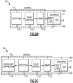
- FIG. 2B is a schematic diagram of a portion of an IC interface 30 including overstress protection according to another embodiment.
- the IC interface 30 includes a supply voltage rail VDD, a ground rail VSS, and an overstress protection circuit including a control circuit 13 and a discharge circuit 4.
- the first interface pad corresponds to a supply voltage rail VDD
- the second interface pad corresponds to a ground rail VSS.
- teachings herein can be used to provide overstress protection to other IC interface pads, including, but not limited to, pads associated with other power domains. Accordingly, other implementations are possible.
- control circuit 13 includes a detection circuit 21, a delay control circuit 22, and a driver circuit 23.
- detection circuit 21 a detection circuit
- delay control circuit 22 a delay control circuit
- driver circuit 23 a driver circuit
- the detection circuit 21 operates to monitor for presence of electrical overstress between the supply voltage rail VDD and the ground rail VSS, and generates a detection signal indicating whether or not presence of an electrical overstress event is detected.
- the detection circuit 21 observes a rate of voltage change between the supply voltage rail VDD and the ground rail VSS, and controls the detection signal based on the observed rate of voltage change.
- the detection circuit 21 can detect for presence of an electrical overstress event based on a multitude of detection conditions indicative of potential damage to sensitive electronics, including, but not limited to, observations of power, voltage, current, and/or charge.
- the detection circuit 21 determines that an electrical overstress event is present in response to detecting a rapidly changing voltage for a sufficient period of time between the supply voltage rail VDD and the ground rail VSS. For instance, in one embodiment the detection circuit 21 activates the detection signal for transient electrical events having a rate of voltage change in the range of about 0.1 V/ns to about 100 V/ns for a length of time in the range of about 1ns to about 1000ns. When an electrical overstress event is not detected, the detection circuit 21 controls the detection signal DET to a signal level associated with no detection of overstress.
- the detection circuit 21 provides the detection signal to the delay control circuit 22.
- the detection circuit 21 Upon detection of an electrical overstress event, the detection circuit 21 activates the detection signal, which the delay control circuit 22 processes to generate a controlling signal.
- the controlling signal is active while the detection signal indicates presence of overstress and for a certain amount of time thereafter.
- the controlling signal can be activated for a time period sufficient for the discharge circuit 4 to discharge the overstress, including a trailing edge of the electrical overstress event.
- the driver circuit 23 operates to buffer, invert, and/or otherwise process the controlling signal to generate at least one trigger signal for the smaller SCR 7 of the discharge circuit 4.
- the control circuit 13 operates to activate trigger signal(s) in response to detecting an electrical overstress event between the supply voltage rail VDD and the ground rail VSS. Additionally, after the overstress is discharged, active control terminates and the discharge circuit 4 is released.
- FIG. 2C is a schematic diagram of a portion of an IC interface 40 including overstress protection according to another embodiment.
- the IC interface 40 includes a supply voltage rail VDD, a ground rail VSS, and an overstress protection circuit including a control circuit 33 and a discharge circuit 4.
- the IC interface 40 of Figure 2C is similar to the IC interface 30 of Figure 2B , except that the control circuit 33 of Figure 2C further includes an overshoot suppression circuit 24.
- Including the overshoot suppression circuit 24 aids in limiting or suppressing an amount of voltage overshoot that occurs before the control circuit 33 is able to activate the discharge circuit 4.
- the discharge circuit 4 has a finite turn-on time, and thus voltage can build-up during a time period before the control circuit 33 activates the discharge circuit 4.
- a secondary discharge path can be activated between the supply voltage rail VDD and the ground rail VSS before a primary discharge path through the discharge circuit 4 is activated.
- the detection circuit 21 provides a detection signal to the overshoot suppression circuit 24.
- the detection signal serves to turn on or off the overshoot suppression circuit 24 to selectively provide a secondary discharge path at the start of an overstress event to discharge a portion of the overstress and limit voltage build-up.
- Figure 2C illustrates the detection circuit 21 as providing separate detection signals to the delay control circuit 22 and the overshoot suppression circuit 24, in certain implementations a common detection signal is provided to the delay control circuit 22 and the overshoot suppression circuit 24.
- Figure 3A is an annotated cross-section of an SCR 100 according to one embodiment.
- the SCR 100 illustrates one example implementation of an SCR that can be included in a discharge circuit.
- one or more instantiations of the SCR 100 can be used to implement the smaller SCR 7 and/or larger SCR 8 of Figures 2A-2C .
- the SCR 100 can have a geometry (for instance, device width) selected to achieved desired current handling capability.
- an SCR Although one specific implementation of an SCR is shown in Figure 3A , the teachings herein are applicable to discharge circuits that include SCRs implemented in a wide variety of ways.
- an SCR can include different configurations of semiconductor wells and/or active regions.
- the SCR 100 of Figure 3A is fabricated in a p-type substrate (P-SUB) 80, and includes an n-type well (NW) 81, a p-type well (PW) 82, an anode p-type active (P+) region 91, a cathode P+ region 92, a trigger P+ region 93, an anode n-type active (N+) region 95, a cathode N+ region 96, a trigger N+ region 97, and shallow trench isolation (STI) regions 98.
- NW n-type well
- PW p-type well
- P+ anode p-type active
- a cathode P+ region 92 a cathode P+ region 92
- a trigger P+ region 93 an anode n-type active (N+) region 95, a cathode N+ region 96, a trigger N+ region 97, and shallow trench isolation (STI) regions 98
- the NW 81 and the PW 82 are formed in the P-SUB 80 adjacent to one another. Additionally, the anode N+ region 95, the anode P+ region 91, and the trigger N+ region 97 are formed in the NW 81, with the anode P+ region 91 positioned between the anode N+ region 95 and the trigger N+ region 97. Additionally, the anode N+ region 95 and the anode P+ region 91 are electrically connected to an anode terminal (ANODE) of the SCR 100 via metallization. Furthermore, the trigger N+ region 97 is electrically connected to a first trigger terminal (TN) via metallization. A trigger terminal is also referred to herein as a control terminal or a control input.
- the trigger P+ region 93, the cathode N+ region 96, and the cathode P+ region 92 are formed in the PW 82.
- the cathode N+ region 96 is positioned between the trigger P+ region 93 and the cathode P+ region 92.
- the cathode N+ region 96 and the cathode P+ region 92 are electrically connected to a cathode terminal (CATHODE) of the SCR 100 via metallization.
- the trigger P+ region 93 is electrically connected to a second trigger terminal (TP) via metallization.
- the electrical connections to the SCR's terminals are schematically depicted in Figure 3A , and can correspond to electrical connections made using contacts and metallization during back end processing.
- the P-SUB 80 includes other devices formed therein.
- the illustrated embodiment includes STI regions 98. Formation of the STI regions 98 can include etching trenches in the P-SUB 80, filling the trenches with a dielectric, such as silicon dioxide (SiO 2 ), and removing the excess dielectric using any suitable method, such as chemical-mechanical planarization.
- a dielectric such as silicon dioxide (SiO 2 )
- the NW 81 and the PW 82 have a depth into the P-SUB 80 that is greater than a depth into the P-SUB 80 than both the STI regions 98 and the P+ and N+ active regions. Additionally, the STI regions 98 have a depth into the P-SUB 80 that is greater than that of the N+ and P+ regions. Furthermore, the N+ active regions have a higher n-type doping concentration than the NW 81. Additionally, the P+ active regions have a higher p-type doping concentration than the PW 82, which in turn has a higher doping concentration than the P-SUB 80.
- the SCR 100 has been further annotated to show certain circuit devices present in the cross-section, including a PNP bipolar device Q1, an NPN bipolar device Q2, an NW resistor R nw and a PW resistor R pw.
- the PNP bipolar device Q1 includes an emitter formed from the anode P+ region 91, a base formed from the NW 81, and a collector formed from the PW 82.
- the NPN bipolar device Q2 includes an emitter formed from the cathode N+ region 96, a base formed from the PW 82, and a collector formed from the NW 81.
- the NW resistor R nw is formed from a resistance of the NW 81 between the collector of the NPN bipolar transistor Q2 and the anode terminal.
- the PW resistor R pw is formed from a resistance of the PW 82 between the collector of the PNP bipolar transistor Q1 and the cathode terminal.
- the first trigger terminal (TN) and/or the second trigger terminal (TP) can receive a trigger signal for activating the SCR 100.
- the trigger signal(s) can be provided by a control circuit, such as any of the control circuits of Figures 2A , 2B , 2C , or 5 .
- the control circuit controls the trigger signal(s) to turn off the SCR 100.
- the control circuit detects an electrical overstress event, the control circuit turns on the SCR 100 to clamp the anode terminal and the cathode terminal to reduce overvoltage conditions. After the overstress is discharged, the trigger signal(s) are deactivated to turn off the SCR 100.
- the trigger N+ region 97 and the trigger P+ region 93 are located in a central region of the SCR 100, and between the active regions associated with the SCR's anode and cathode terminals.
- trigger control at the center of the SCR 100 By providing trigger control at the center of the SCR 100, reduced input resistance to the base terminals of the NPN and PNP bipolar transistors is provided, thereby contributing to rapid SCR turn on time. Moreover, triggering is provided in a region of the SCR 100 in which carrier multiplication and/or recombination processes associated with regenerative feedback of the coupled PNP bipolar transistor Q1 and NPN bipolar transistor Q2 occurs. Thus, low-resistance trigger control at the center of the SCR 100 facilitates activation and deactivation of SCR conduction in a region in which regenerative feedback takes place, with a relatively small impact on SCR on-state resistance.
- Figure 3B is a circuit diagram 110 of the SCR 100 of Figure 3A .
- the circuit diagram 110 includes the PNP bipolar device Q1, the NPN bipolar device Q2, the NW resistor R nw , and the PW resistor R pw.
- the emitter of the PNP bipolar transistor Q1 is electrically connected to the anode terminal, and the collector of the PNP bipolar transistor Q1 is electrically connected to the cathode terminal via the PW resistor R pw. Additionally, the base of the PNP bipolar transistor Q1 is electrically connected to the collector of the NPN bipolar transistor Q2. Furthermore, the first trigger terminal TN is electrically connected to the base of the PNP bipolar transistor Q1.
- the emitter of the NPN bipolar transistor Q2 is electrically connected to the cathode terminal, and the collector of the NPN bipolar transistor Q2 is electrically connected to the anode terminal via the NW resistor R nw . Additionally, the base of the NPN bipolar transistor Q2 is electrically connected to the collector of the PNP bipolar transistor Q1. Furthermore, the second trigger terminal TP is electrically connected to the base of the NPN bipolar transistor Q2.
- Figure 4A is an annotated cross-section of an SCR 120 according to another embodiment.
- the SCR 120 of Figure 4A is similar to the SCR 100 of Figure 3A , except that the SCR 120 of Figure 4A further includes a first SCR-characteristic adjustment circuit 111 and a second SCR-characteristic adjustment circuit 112.
- the first SCR-characteristic adjustment circuit 111 is connected between the anode terminal and the anode N+ region 95
- the second SCR-characteristic adjustment circuit 112 is connected between the cathode terminal and the cathode P+ region 92.
- Including the first SCR-characteristic adjustment circuit 111 and/or the second SCR-characteristic adjustment circuit 112 can aid in providing control over various characteristics of the SCR 120, such as the SCR's trigger voltage.
- the NPN bipolar transistor Q1 operates with a breakdown voltage collector-emitter open (BVCEO) characteristic, which can lower the SCR's trigger voltage but also increase off-state leakage current.
- BVCEO breakdown voltage collector-emitter open
- the first SCR-characteristic adjustment circuit 111 and/or the second SCR-characteristic adjustment circuit 112 can be included to provide fine-tuned controlled over various parameters or characteristics of the SCR 120, thereby providing performance adjustment suitable for a particular implementation and/or application.
- An SCR-characteristic adjustment circuit can be implemented in a wide variety of ways, including, for example, using passive and/or active circuit components. In certain implementations, all or part of an SCR-characteristic adjustment circuit is implemented in a portion of the P-SUB 80, for instance, adjacent to a layout of the SCR's bipolar transistors.
- Figure 4A illustrates an embodiment including both the first SCR-characteristic adjustment circuit 111 and the second SCR-characteristic adjustment circuit 112
- teachings herein are also applicable to implementations including the first SCR-characteristic adjustment circuit 111 and omitting the second SCR-characteristic adjustment circuit 112 and to implementations including the second SCR-characteristic adjustment circuit 112 and omitting the first SCR-characteristic adjustment circuit 111.
- Figure 4B is a circuit diagram 130 of the SCR 120 of Figure 4A .
- the circuit diagram 130 of Figure 4B is similar to the circuit diagram 110 of Figure 3B , except that the first SCR-characteristic adjustment circuit 111 and the second SCR-characteristic adjustment circuit 112 are included.
- the first SCR-characteristic adjustment circuit 111 is connected between the NW resistor R nw and the anode terminal
- the second SCR-characteristic adjustment circuit 112 is connected between the PW resistor R pw and the cathode terminal.
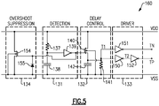
- FIG. 5 is a circuit diagram of another embodiment of a control circuit 160 for controlling activation and shutdown of a discharge circuit.
- the control circuit 160 is electrically connected between a supply voltage rail VDD and a ground rail VSS, and includes a detection circuit 131, a delay control circuit 132, a driver circuit 133, and an overshoot suppression circuit 134.
- a control circuit can be implemented in a wide variety of ways.
- a control circuit can include components and/or sub-circuits implemented in a wide variety of ways to meet performance specifications associated with a particular implementation and/or application.
- the detection circuit 131 includes a detection resistor 137 and a detection capacitor 138 electrically connected in series between the supply voltage rail VDD and the ground rail VSS. Additionally, the detection circuit 131 includes a detection inverter 139 including an input connected to a node between the detection resistor 137 and the detection capacitor 138, and an output that generates a detection signal indicating whether or not an overstress event has been detected. In this example, a logically high value of the detection signal indicates that overstress is present. In another implementation, a logically low value of the detection signal is used to indicate presence of overstress.
- the detection signal generated by the detection inverter 139 is logically low.
- the voltage drop across the detection resistor 137 turns on a PMOS transistor of the detection inverter 139, thereby controlling the detection signal to a logically high value.
- the resistance of the detection resistor 137 and the capacitance of the detection capacitor 138 can be sized to activate in response to a transient signal associated with overstress (for instance, an ESD event), while not falsely activating in response to chip power-on and/or normal operating conditions associated with slow transient voltage change (dV/dt) between the power rails.
- the delay control circuit 132 includes an NMOS transistor 140, a delay control resistor 141, and a delay control capacitor 142.
- the NMOS transistor 140 includes a gate that receives the detection signal from the detection circuit 131. When the detection signal is logically high, the NMOS transistor 140 turns on and charges the delay control capacitor 142. After the detection signal falls to a logically low value, the delay control capacitor 142 discharges via the delay control resistor 141.
- the asymmetric resistance values used for charging (a resistance of NMOS transistor 140) and discharging (a resistance of the delay control resistor 141) allow for sample and holding of the logic control level.
- the first controlling signal T1 can be kept logic high for a desired time period (for instance, a few hundred nanoseconds) by selection of a resistor-capacitor (RC) time constant associated with the delay control resistor 141 and the delay control capacitor 142.
- RC resistor-capacitor
- the driver circuit 160 includes an inverter 150, a first driver 151, and a second driver 152.
- the first driver 151 inverts the first controlling signal T1 to generate a first trigger signal TN.
- the inverter 150 inverts the first controlling signal T1 to generate a second controlling signal T2, which is inverted by the second driver 152 to generate a second trigger signal TP.
- the first trigger signal TN and/or the second trigger signal TP can be used to control activation of a discharge circuit.
- the driver circuit 160 also includes an overshoot suppression circuit 134 for mitigating voltage overshoot associated with finite activation time of the discharge circuit controlled by the driver circuit 160.
- the overshoot suppression circuit 134 includes an NMOS transistor 154 connected between the supply voltage rail VDD and the ground rail VSS, and selectively activated by the detection signal from the detection circuit 131.
- the overshoot suppression circuit 134 operates to limit voltage overshoot between the supply voltage rail VDD and the ground rail VSS before the primary discharge circuit is turned on by the trigger signals TN and/or TP.
- the overshoot protection circuit 134 also includes the diode 155, which serves to protect the NMOS transistor 154 from damage by limiting the transistor's gate-to-source voltage.
- FIG 6A is a circuit diagram of one embodiment of a discharge circuit 200.
- the discharge circuit 200 includes a smaller SCR 207 and a larger SCR 208.
- the smaller SCR 207 and/or the larger SCR 208 can be implemented in a wide variety of ways, including, but not limited to, using the SCR configurations shown in Figures 3A and/or 4A with appropriately selected geometries. However, the smaller SCR 207 and/or the larger SCR 208 can be implemented in other ways.
- the smaller SCR 207 includes a first trigger terminal that receives a first trigger signal TN and a second trigger terminal that receives a second trigger signal TP.
- the first trigger signal TN and the second trigger signal TP can be generated in a wide variety of ways, including, but not limited to, using the discharge circuit 160 of Figure 5 .
- the illustrated embodiment illustrates a configuration in which two trigger signals are used, the teachings herein are also applicable to implementations using more or fewer trigger signals.
- the smaller SCR 207 also includes an anode terminal connected to a first trigger terminal of the larger SCR 208, and to the supply voltage rail VDD via an anode resistor R n .
- the small SCR 207 further includes a cathode terminal connected to a second trigger terminal of the larger SCR 208, and to the ground rail VSS via a cathode resistor R p .
- the larger SCR 208 includes an anode terminal connected to the supply voltage rail VDD, and a cathode terminal connected to the ground rail VSS.
- the anode resistor R n and the cathode resistor R p are explicit resistors provided in addition to parasitic well resistances of the SCRs 207, 208.
- the anode resistor R n and the cathode resistor R p are implemented as diffusion resistors.
- the anode resistor R n and the cathode resistor R p are implemented as thin film resistors and/or polysilicon resistors with high current handling capability.
- a diffusing resistor is implemented with substrate isolation to avoid breakdown between the supply voltage rail VDD and substrate.
- the smaller SCR 207 serves to amplify the trigger signals TN and TP, thereby expediting turn-on time of the larger SCR 208. Accordingly, the benefits of both fast turn-on time and high on-state current handling capability can be achieved.
- FIG. 6B is a circuit diagram of another embodiment of a discharge circuit 220.
- the discharge circuit 220 of Figure 6B is similar to the discharge circuit 200 of Figure 6A , except that the discharge circuit 220 illustrates a specific implementation in which the smaller SCR 217 and the larger SCR 218 are each implemented with an instantiation of the SCR of Figures 3A and 3B .
- the SCRs are implemented with different device areas, such as different device widths and/or number of device fingers.
- the smaller SCR 217 includes a PNP bipolar transistor Q1, an NPN bipolar transistor Q2, an NW resistor R nw , and a PW resistor R pw .
- the larger SCR 218 includes a PNP bipolar transistor Q1', an NPN bipolar transistor Q2', an NW resistor R nw ', and a PW resistor R pw '.
- FIG. 6C is a circuit diagram of another embodiment of a discharge circuit 230.
- the discharge circuit 230 of Figure 6C is similar to the discharge circuit 200 of Figure 6A , except that the discharge circuit 230 of Figure 6C illustrates an implementation in which the anode resistor R n and the cathode resistor R p are omitted in favor of including a PMOS transistor 221 and an NMOS transistor 222, respectively.
- the PMOS transistor 221 has a gate controlled by a first controlling signal T1, which can be generated, for example, using the control circuit 160 of Figure 5 .
- the NMOS transistor 222 has a gate controlled by a second controlling signal T2, which can be generated, for example, using the control circuit 160 of Figure 5 .
- the first SCR 207 is connected to the supply voltage rail VDD and/or the ground rail VSS using both resistors and transistors.
- a resistor and a transistor are included between the anode of the first SCR and the supply voltage rail VDD and/or between the cathode of the first SCR and the ground rail VSS.
- a resistor is included between the anode of the first SCR and the supply voltage rail VDD and a transistor is included between the cathode of the second SCR and the ground rail VSS.
- a transistor is included between the anode of the first SCR and the supply voltage rail VDD and a resistor is included between the cathode of the second SCR and the ground rail VSS.
- Figure 7A is an annotated circuit diagram of one embodiment of a discharge circuit 280 during turn-on.
- Figure 7B is an annotated circuit diagram of one embodiment of a discharge circuit 280 during turn-off.
- Figure 7C is one example of a graph of voltage versus current for an SCR.
- the discharge circuit 280 of Figures 7A and 7B is similar to the discharge circuit 220 of Figure 6B , except that the discharge circuit 280 has been illustrated with various annotations describing one example of turn-on and turn-off operation.
- NPN bipolar transistor Q1 and resistor R n operate as a first emitter follower
- PNP bipolar transistor Q2 and resistor R n operate as a second emitter follower
- the first and second emitter followers operate to amplify current of the first trigger signal TN and the second trigger signal TP, respectively.
- the amplified output currents from the emitter followers operate to turn on NPN bipolar transistor Q1' and PNP bipolar transistor Q2' associated with the larger SCR.
- the parameters for the SCR devices can be selected in a wide variety of ways. Directions of currents for turn-on are annotated in Figure 7A . During turn-on, the smaller SCR can conduct before the larger SCR.
- the current I n through NW resistor R nw ' flows into the smaller SCR, since initially I p and I SCR2 currents are close to zero because the larger SCR has not yet turned on.
- the voltage drops on both resistor R n and NW resistor R nw ' are roughly the forward bias of a p-n junction (for instance, V d or about 0.6V ⁇ 0.8V).
- Equation 1 is constrained by Equation 2 below, in which I t 2 ,SCR 1 and I h,SCR 1 are the smaller SCR's failure current and holding current, respectively.
- Equation 2 the variables of Equation 2 are replaced using normalized (to width) values, yielding Equation 3 below.
- a 1 and A 2 represent the widths of the smaller SCR and the larger SCR, respectively.
- I h ⁇ , I t 2 ⁇ and R nw ⁇ values can be obtained from testing or simulation of one or more SCRs.
- the voltage increases linearly with current.
- the slope is defined by on resistance R on , and for specified current I SCR , the voltage drop is given by Equation 4 below.
- V SCR 2 V d + I SCR R on
- the smaller SCR has an on-state resistance R1 and the larger SCR has an on-state resistance of R2.
- the current through R n and R nw can be given by Equation 5 below, where I h,SCR 2 is the holding current of the larger SCR.
- I R + I n V d R n / / R nw ⁇ I h , SCR 2
- the larger SCR is implemented such that at holding point, the voltage V DD between power rail and ground rail is given by Equation 6 below.
- Equation 6 Implementing the overstress protection circuit in this manner aids in mitigating latch-up risks. 2 V d + I h . SCR 2 R 2 > V DD
- Equation 1 is combined with Equation 6 to yield Equation 7 below. 2 V d + V d R n / / R nw R 2 > V DD
- one or more of the Equations provided above are used to obtain values for A 1 , A 2 , and/or R n .
- FIG. 8 is a schematic diagram of one embodiment of an IC 300 implemented with overstress protection.
- the IC 300 includes a first conductor 301, a second conductor 302, core circuitry 209, and overstress protection circuitry including a control circuit 303, first to third trigger distribution circuits 315a-315c, first to third smaller SCRs 207a-207c, first to third larger SCRs 208a-208c, first to third anode resistors R na , R nb , R nc , and first to third cathode resistors R pa , R pb , R pc .
- IC 300 Although one specific embodiment of an IC 300 is shown in Figure 8 , the teachings herein are applicable to ICs implemented in a wide variety of ways, including, but not limited to, ICs implemented with more or fewer control circuits and/or discharge circuits. Furthermore, ICs can include different configurations of circuitry protected by an overstress protection circuit. Accordingly, although Figure 8 illustrates one specific implementation of an IC, other IC implementations are possible.
- the first conductor 301 carries a supply voltage VDD received from one or more supply voltage pads (not shown in Figure 8 ), and the second conductor 301 carries a ground voltage VSS received from one or more ground pads (not shown in Figure 8 ).
- VDD supply voltage
- VSS ground voltage
- teachings here can be used to provide overstress protection to other power domains. Accordingly, other implementations are possible.
- the first conductor 301 and the second conductor 302 are schematically depicted as rings for providing power supply distribution about the IC 300, including to core circuitry 209.
- the core circuitry 209 can include a wide variety of circuitry, such as digital circuitry, analog circuitry, radio frequency circuitry, and/or mixed-signal circuitry.
- the conductors are illustrated as rings, supply distribution conductors can be implemented in a wide variety of ways.
- a conductive network for distributing a power supply can include conductors on multiple metallization layers of an IC. In Figure 9 , the conductors are depicted as including parasitic resistors.
- the control circuit 303 includes a detection circuit 311 that generates a detection signal based on monitoring a voltage difference between the first conductor 301 and the second conductor 302. Additionally, the control circuit 303 includes a delay control circuit 312 for generating a controlling signal based on the detection signal. Furthermore, the control circuit 303 further includes a driver circuit 313 which generates a first trigger signal and a second trigger signal based on the controlling signal. The first and second trigger signals are provided to the trigger distribution circuits 315a-315c, which serve to distribute the triggers signals to the smaller SCRs 207a-207c. The smaller SCRs 207a-207c in turn controls selective activation of the larger SCRs 208a-208c, respectively.
- multiple discharge circuits are provided. Including multiple discharge circuits can aid in limiting overvoltage across different regions of the IC 300. For example, resistive and/or inductive effects associated with conductors used for power supply distribution can lead to voltage drops and different electrical potentials at different positions along the conductors.
- FIGS 9A-9C illustrate various examples of simulated waveforms for various overstress protection circuits. The results correspond to data generated using mixed-mode simulation using Synopsys Sentaurus.
- Overstress protection circuits Four types are simulated.
- each figure includes a first plot ("SCR") of a single SCR providing protection without using a control circuit, a second plot ("Control+SCR") of a single SCR controlled by a control circuit, a third plot (“Control+MOS”) of a single NMOS transistor with a width of 1200 ⁇ m controlled by a control circuit, and a fourth plot ("Control+Dual-SCR”) of an overstress protection circuit using one implementation of the discharge circuit 200 of Figure 6A and the control circuit 160 of Figure 5 .
- Figure 9A is one example of simulated waveforms of voltage versus time for the overstress protection circuits described above for an IC in a power-on state.
- Figure 9B is another example of simulated waveforms of voltage versus time for the overstress protection circuits described above for an IC in a power-on state.
- Figures 9A and 9B correspond to the same simulation, but with different time scales.
- the power-on state simulation emulates overstress when the IC is biased and fully operational.
- VDD is initially set to 5V.
- TLP transmission line pulse
- the pulse simulates one example of an electrical overstress event.
- the single SCR has the highest overshoot voltage. Additionally, the single SCR undesirably remains in a latch-up condition after the pulse is removed at about 220ns.
- the overshoot is improved.
- the NMOS transistor can be turned-off by the control circuit, as shown by the voltage of VDD eventually recovering to 5V.
- the big NMOS transistor has a relatively high on-resistance, as shown by the clamping voltage approaching 7V at 1A.
- control circuit and dual-SCR has a comparable overshoot voltage to the control circuit and NMOS transistor, and advantageously handles more stress current with a smaller circuit layout.
- the dual-SCR can be turned off by the control circuit, eliminating latch-up concerns.
- Figure 9C is another example of simulated waveforms of voltage versus time for the overstress protection circuits described above for an IC in a power-off state.
- the IC's power supplies are powered-down.
- the initial voltage on VDD is 0 volts.
- a 1 amp TLP pulse with 10ns rising time and 100ns pulse width is applied.
- the overshoot voltage of the single SCR is relative high, for instance, up to about 40 V higher than that of the control circuit and dual-SCR.
- control circuit fails to turn on the single SCR effectively.
- control circuit and large NMOS transistor shows low voltage overshoot, on-resistance of the NMOS is relatively high, resulting in a clamping voltage of about ⁇ 6V.
- control circuit and dual-SCR provides a similar transient performance as the control circuit and large NMOS transistor, but provides a superior clamping voltage (corresponding to lower on-state resistance) and occupies a smaller layout area.
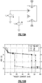
- Figure 10A is a schematic diagram of a simulation setup for an SCR. As shown in Figure 10A , a first current source I_tn and a second current source I_tp drive a first trigger terminal TN and a second trigger terminal TP, respectively, of an SCR.
- Figure 10B is one example of simulated trigger current versus voltage for the simulation setup of Figure 10A .
- using both a first trigger signal to control the first trigger terminal TN and a second trigger terminal TP reduces an amount of trigger current to activate the SCR.
- using multiple trigger signals enhances performance relative to implementations using a single trigger signal.
- the teachings herein are also applicable to implementations using one trigger signal.
- simulation results can vary based on a wide range of factors, such as circuit implementation, simulation parameters, models, and/or tools. Accordingly, other waveforms are possible.
- Devices employing the above-described schemes can be implemented into various electronic devices.
- Examples of the electronic devices can include, but are not limited to, consumer electronic products, parts of the consumer electronic products, electronic test equipment, communication infrastructure applications, etc. Further, the electronic device can include unfinished products, including those for communication, industrial, medical and automotive applications.
- p-type regions can include a p-type semiconductor material, such as boron, as a dopant.
- n-type regions can include an n-type semiconductor material, such as phosphorous, as a dopant. Persons having ordinary skill in the art will appreciate various concentrations of dopants in regions described above.
Landscapes
- Engineering & Computer Science (AREA)
- Microelectronics & Electronic Packaging (AREA)
- Physics & Mathematics (AREA)
- General Physics & Mathematics (AREA)
- Semiconductor Integrated Circuits (AREA)
- Power Engineering (AREA)
Abstract
Description
- Embodiments of the invention relate to electronic systems, and more particularly, to systems and devices for electrical overstress protection and latch-up prevention.
- Certain electronic systems can be exposed to electrical overstress events, or electrical signals of short duration having rapidly changing voltage and high power. Electrical overstress events can include, for example, electrostatic discharge (ESD) events arising from the abrupt release of charge from an object or person to an electronic system.
- Electrical overstress events can damage or destroy integrated circuits (ICs) by generating overvoltage conditions and high levels of power dissipation in relatively small areas of the ICs. High power dissipation can increase IC temperature, and can lead to numerous problems, such as gate oxide punch-through, junction damage, metal damage, and surface charge accumulation.
- Overstress protection circuits for providing protection from electrical overstress are provided. In certain implementations, a semiconductor chip includes a control circuit that activates a discharge circuit to protect the chip from damage when an overstress event is detected. To provide both fast protection speed and ability to handle large amounts of overstress, the discharge circuit includes a smaller but faster first silicon controlled rectifier (SCR) that turns on a larger but slower second SCR.
- In one aspect, a semiconductor die includes a first pad, a second pad, a control circuit configured to activate at least one trigger signal in response to detecting an electrical overstress event between the first pad and the second pad, and a discharge circuit electrically connected between the first pad and the second pad and including a first SCR and a second SCR. The first SCR is configured to turn on the second SCR in response to activation of the at least one trigger signal to thereby discharge the electrical overstress event.
- In one example, the second SCR has a larger device area than the first SCR.
- Moreover, in another example, an anode of the first SCR is electrically connected to a first control input of the second SCR, and a cathode of the first SCR is electrically connected to a second control input of the second SCR.
- In one example, the first SCR comprises an NPN bipolar transistor and a PNP bipolar transistor that are cross-coupled, wherein the at least one trigger signal comprises at least one of a first trigger signal provided to a base of the NPN bipolar transistor or a second trigger signal provided to a base of the PNP bipolar transistor. Furthermore, at least one of a first resistor or a first field-effect transistor (FET) may be electrically connected between an anode of the first SCR and the first pad, and at least one of a second resistor or a second FET electrically connected between a cathode of the first SCR and the second pad.
- In some examples, the first pad comprises a power supply rail and the second pad comprises a ground rail. Moreover, in further examples the control circuit may comprise a detection circuit configured to activate a detection signal in response to detecting presence of the electrical overstress event, a delay control circuit configured to generate a controlling signal based on the detection signal, the controlling signal being active for a longer duration than the detection signal, and a driver circuit configured to generate the at least one trigger signal based on the controlling signal.
- In one example the control circuit may further comprise an overshoot protection circuit electrically connected between the first pad and the second pad, wherein the detection circuit is further configured to turn on the overshoot protection circuit in response to detecting presence of the electrical overstress event.
- In another aspect, a method of electrical overstress protection is provided. The method includes detecting for presence of an electrical overstress event between a first pad and a second pad of an electronic interface, activating at least one trigger signal in response to detecting the electrical overstress event, turning on a first SCR in response to activation of the least one trigger signal, and turning on a second SCR to clamp the first pad and the second pad using the first SCR.
- In one example the method may further comprise amplifying a first trigger signal of the at least one trigger signal using a PNP bipolar transistor of the first SCR, and amplifying a second trigger signal of the at least one trigger signal using an NPN bipolar transistor of the first SCR.
- Moreover, in another example the detecting for presence of the electrical overstress event may comprise activating a detection signal in response to detecting the electrical overstress event, generating a controlling signal based on the detection signal, the controlling signal being active for a longer duration than the detection signal, and buffering the controlling signal to generate the at least one trigger signal.
- In a yet further example, the method may also further comprise limiting voltage overshoot by activating a secondary discharge path between the first pad and the second pad through an overshoot protection circuit before activating a primary discharge path through the second SCR.
- In another aspect, an interface for a semiconductor chip is provided. The interface includes a first interface pad, a second interface pad, a control circuit configured to detect for presence of an electrical overstress event between the first interface pad and the second interface pad, and to activate at least one trigger signal in response to detecting the electrical overstress event, and a discharge circuit. The discharge circuit includes a first SCR configured to receive the at least one trigger signal and to turn on in response to activation of the at least one trigger signal, and a second SCR electrically connected between the first interface pad and the second interface pad. The first SCR is configured to selectively turn on or turn off the second SCR based on amplifying the at least one trigger signal.
- In one example of the interface the second SCR has a larger device area than the first SCR.
- Moreover, in one example of the interface, an anode of the first SCR is electrically connected to a first control input of the second SCR, and a cathode of the first SCR is electrically connected to a second control input of the second SCR.
- Furthermore, in one example of the interface the first SCR comprises an NPN bipolar transistor and a PNP bipolar transistor that are cross-coupled, wherein the at least one trigger signal comprises at least one of a first trigger signal provided to a base of the NPN bipolar transistor or a second trigger signal provided to a base of the PNP bipolar transistor.
- A further example of the interface may further comprise a first resistor electrically connected between an anode of the first SCR and the first interface pad, and a second resistor electrically connected between a cathode of the first SCR and the second interface pad.
- Another example of the interface may further comprise a first field-effect transistor (FET) electrically connected between an anode of the first SCR and the first interface pad, and a second FET electrically connected between a cathode of the first SCR and the second interface pad.
- In one example of the interface the first interface pad comprises a power supply rail and the second interface pad comprises a ground rail.
- In one example of the interface the control circuit further comprises an overshoot protection circuit electrically connected between the first interface pad and the second interface pad, wherein the detection circuit is further configured to limit voltage overshoot by activating a secondary discharge path through the overshoot protection circuit before activating a primary discharge path through the second SCR.
-
-
Figure 1A is a schematic diagram of one example of a vehicle including various electronic vehicle systems that are connectable via one or more vehicle systems interfaces. -
Figure 1B is a schematic diagram of one embodiment of an integrated circuit (IC) that is connectable to a vehicle systems interface or other communication interface. -
Figure 2A is a schematic diagram of a portion of an IC interface including overstress protection according to one embodiment. -
Figure 2B is a schematic diagram of a portion of an IC interface including overstress protection according to another embodiment. -
Figure 2C is a schematic diagram of a portion of an IC interface including overstress protection according to another embodiment. -
Figure 3A is an annotated cross-section of a silicon controlled rectifier (SCR) according to one embodiment. -
Figure 3B is a circuit diagram of the SCR ofFigure 3A . -
Figure 4A is an annotated cross-section of an SCR according to another embodiment. -
Figure 4B is a circuit diagram of the SCR ofFigure 4A . -
Figure 5 is a circuit diagram of another embodiment of a control circuit for controlling activation and shutdown of a discharge circuit. -
Figure 6A is a circuit diagram of one embodiment of a discharge circuit. -
Figure 6B is a circuit diagram of another embodiment of a discharge circuit. -
Figure 6C is a circuit diagram of another embodiment of a discharge circuit. -
Figure 7A is an annotated circuit diagram of one embodiment of a discharge circuit during turn-on. -
Figure 7B is an annotated circuit diagram of one embodiment of a discharge circuit during turn-off. -
Figure 7C is one example of a graph of voltage versus current for an SCR. -
Figure 8 is a schematic diagram of one embodiment of an IC implemented with overstress protection. -
Figure 9A is one example of simulated waveforms of voltage versus time for various overstress protection circuits. -
Figure 9B is another example of simulated waveforms of voltage versus time for various overstress protection circuits. -
Figure 9C is another example of simulated waveforms of voltage versus time for various overstress protection circuits. -
Figure 10A is a schematic diagram of a simulation setup for an SCR. -
Figure 10B is one example of simulated trigger current versus voltage for the simulation setup ofFigure 10A . - The following detailed description of certain embodiments presents various descriptions of specific embodiments of the invention. However, the invention can be embodied in a multitude of different ways as defined and covered by the claims. In this description, reference is made to the drawings where like reference numerals may indicate identical or functionally similar elements. It will be understood that elements illustrated in the figures are not necessarily drawn to scale. Moreover, it will be understood that certain embodiments can include more elements than illustrated in a drawing and/or a subset of the elements illustrated in a drawing. Further, some embodiments can incorporate any suitable combination of features from two or more drawings.
- To help guarantee that an integrated circuit (IC) is reliable, manufacturers can test the IC under defined stress conditions, which can be described by standards set by various organizations, such as the Joint Electronic Device Engineering Council (JEDEC), the International Electrotechnical Commission (IEC), and the Automotive Engineering Council (AEC). The standards can cover a wide multitude of transient electrical overstress events, including electrostatic discharge (ESD) events. To provide protection from electrical overstress, the IC's interface can include electrical overstress protection circuits. An IC is also referred to herein as a semiconductor die or chip.
- One type of overstress protection circuit is a power supply clamp, which during an overstress event provides a high current discharge path and voltage clamping between a pair of power rails, such as a supply voltage rail and a ground rail. The performance of a power supply clamp aids in meeting or exceeding specifications with respect to IC-level stress conditions and/or system-level stress conditions. Such clamps are used to not only help in minimizing electrically-induced-physical-damage arising from electrical overstress, but also in preventing unintended latch-up triggering conditions. Latch-up can be triggered, for instance, by elevated transient overvoltage between the power rails due to limitations in the ESD clamping response time of the power supply clamp. For example, electrical overstress events cause transient high current injection into an IC's substrate, which can lead to current-induced triggering of parasitic bipolar devices present in circuit layouts.
- Different combination of devices and circuits can be used to implement a power supply clamp. For example, a resistor-capacitor (RC) network can serve as a detector for activating a large current handling capability device. For instance, the detector can generate a controlling signal to turn on the large current handling capability device in response to detecting transient overstress between the power rails. After activation, the large current handling capability device can provide a low-resistance current path until subsequent deactivation.
- To reduce leakage, a large n-type metal oxide semiconductor (NMOS) transistor can be used as a large current handling capability device in CMOS and BCDMOS process technologies. The large NMOS transistor operates in active mode and has a gate voltage controlled by a controlling circuit. However, a large NMOS transistor can suffer from relatively low current density in active mode, which creates a desire for large transistor area utilization to compensate for the transistor's low current handling capability efficiency.
- To achieve both high current handling capability and low on-state resistance, the large NMOS transistor occupies more layout area as compared to other devices that can operate in bipolar mode, for instance, a silicon controlled rectifier (SCR). Although devices that operate in bipolar mode provide high current handling capability, devices that operate in bipolar mode typically operate using a much higher driving current for control relative to large NMOS transistors. Thus, a controlling circuit may have difficulty in effectively activating and shutting down a device that operates in bipolar mode.
- Apparatus and methods for electrical overstress protection are provided herein. In certain configurations, an overstress protection circuit includes a control circuit for detecting presence of an overstress event between a first pad and a second pad of an interface, and a discharge circuit electrically connected between the first pad and the second pad and selectively activated by the control circuit. In certain implementations, the first pad and the second pad correspond to a pair of power supply rails, for instance, a supply voltage rail and a ground rail, respectively. The discharge circuit includes a first or smaller SCR and a second or larger SCR. In response to detecting an overstress event, the control circuit activates the smaller SCR, which in turn activates the larger SCR to provide clamping between the first pad and the second pad.
- The control circuit operates to actively control the SCR-based discharge circuit to initiate and interrupt regenerative feedback, thereby controlling turn-on and turn-off of the discharge circuit. For example, one or more trigger signals can be provided to one or more bases of a coupled pair of PNP and NPN bipolar transistors of the smaller SCR to thereby control carrier multiplication and/or recombination processes associated with regenerative feedback of the coupled pair. The smaller SCR in turn controls one or more bases of a coupled pair of PNP and NPN bipolar transistors of the larger SCR.
- The smaller SCR serves to amplify the trigger signal(s) received from the control circuit, and thus can more efficiently drive the larger SCR between on and off states. Thus, implementing the discharge circuit using multiple SCRs provides more robust control over activating and shutting down the discharge circuit. Accordingly, faster turn-on time, lower voltage overshoot, and/or quicker turn-off time can be achieved while maintaining the benefits of high current handling capability provided by a bipolar mode discharge circuit.
- In certain implementations, multiple SCR-based discharge circuits are distributed throughout different regions of the IC. When activated during high transient electrical overstress, the SCR-based discharge circuits assist in providing a temporary low impedance discharge path and voltage clamping function.
- The teachings herein can be used in a wide variety of applications, including, but not limited to, industrial, instrumentation, energy, healthcare, automation, automotive communication, and diagnostic applications. For example, emerging mission critical applications can be specified to tolerate stress conditions that are much higher than typical overstress characterization. The overstress protection circuits herein can be used not only to provide protection during power-off conditions (for instance, during handling or ESD testing), but also during power-on conditions in which the IC receives power. For instance, certain system level applications, such as automotive interfaces, industrial LVDS drivers, satellite automotive sensors, and wired communication interface circuits, can be subject to stress conditions during normal operation.
- The interface can correspond to an electronic interface of an IC, a System on a Chip (SoC), or System in-a-Package (SiP). In certain implementations, the overstress protection circuit is fabricated on a semiconductor die or chip and provides protection to circuitry fabricated on-chip with the overstress protection circuit. However, other configurations are possible. In a first example, the overstress protection circuit is fabricated on a first chip and provides protection to circuitry on a second chip, which can be in a common package or module with the first chip. In a second example, the overstress protection circuit is fabricated on a chip and provides protection to off-chip components, such as surface mount devices.
-
Figure 1A is a schematic diagram of one example of avehicle 1000 including various electronic vehicle systems that are connectable via one or more vehicle systems interfaces. In the illustrated example, thevehicle 1000 includes athrottle actuator system 1001, asteering actuator system 1002, abrake actuator system 1003, a laserrange finder system 1004, a forward-lookingradar system 1005, acamera system 1006, asteering sensor system 1007, a vehiclecontrol computer system 1009, avision computer system 1010, a drive by wire (DBW)controller system 1011, adisplay computer system 1012, and a side-lookingradar system 1013. - The vehicle systems shown in
Figure 1A are connectable to one or more vehicle systems interfaces, such as a local interconnect network (LIN) interface, a controller area network (CAN) interface, an automotive audio bus (A2B) interface, a Fieldbus interface, and/or a wide variety of other communication interfaces or buses. The vehicle systems interfaces are used to provide communication between various vehicle systems, thereby facilitating electronic control and management of thevehicle 1000. Although one example of vehicle systems is depicted inFigure 1A , a vehicle can include a wide range of electronic vehicle systems. - Vehicle systems interfaces can be exposed to a wide range of electrical overstress events. Such electrical overstress events can include not only ESD events, but also voltage spikes resulting from delivering a varying current to an inductive load, overstress events arising from electromagnetic inductive coupling, electrical overstress received by way of load dump from starting an automotive engine, and/or other electrical overstress events.
- The overstress protection circuits herein can be used to provide protection to electronic components, such as semiconductor chips, that are exposed to electrical overstress events via an interface, such a vehicle systems interface. For example, an overstress protection circuit implemented in accordance with the teachings herein can serve as a power clamp between a supply voltage and a ground voltage received over a vehicle systems interface. Although the teachings herein can be used to provide protection to electronic circuitry of a vehicle systems interface, other applications of the technology are possible. For example, the overstress protection circuits herein can be used not only for automotive applications, but also to provide protection to chip interfaces used in industrial, instrumentation, energy, healthcare, control, diagnostic, and/or a wide range of other applications.
-
Figure 1B is a schematic diagram of one embodiment of an integrated circuit (IC) or semiconductor die 1020 that is connectable to a vehicle systems interface or other communication interface. The semiconductor die 1020 includes sensors 1021, ananalog input circuit 1022, a first digital input/output (I/O)circuit 1023, a controller (for instance, a secure microcontroller) 1024, ananalog output circuit 1025, a second digital I/O circuit 1026,actuators 1027, aFieldbus circuit 1028, an isolatedpower supply circuit 1029, and apower clamp 1030. TheIC 1020 can be used for communication interfaces associated with distributed remote nodes including sensors and/or actuators. - In the illustrated embodiment, the
IC 1020 is connectable to a Fieldbus interface or bus via theFieldbus circuit 1028. For example, theIC 1020 can communicate with programmable logic controllers (PLCs) via theFieldbus circuit 1028, thereby aiding in providing real-time distributed control and communication. In the illustrated embodiment, theIC 1020 includes thepower clamp 1030 to provide clamping between a supply voltage and a ground voltage received via the Fieldbus interface. Thepower clamp 1030 can be implemented with one or more features in accordance with the teachings herein. - Although example applications for overstress protection circuits are illustrated in
Figures 1A and 1B , the teachings herein are applicable to a wide range of applications, including, but not limited to, chip interfaces for automotive, industrial, instrumentation, energy, healthcare, automation, and/or diagnostic applications. -
Figure 2A is a schematic diagram of a portion of anIC interface 10 including overstress protection according to one embodiment. TheIC interface 10 includes afirst interface pad 1, asecond interface pad 2, and an overstress protection circuit including acontrol circuit 3 and adischarge circuit 4. - Although not shown in
Figure 2A for clarity of the figures, theIC interface 10 can include a wide variety of additional structures and circuity. For example, theIC interface 10 can include additional pins or pads. Furthermore, theIC interface 10 can include digital circuitry, analog circuitry, radio frequency circuitry, and/or mixed-signal circuitry that is connected to thefirst interface pad 1 and/or thesecond interface pad 2 and protected by the overstress protection circuitry shown inFigure 2A . - The
first interface pad 1 and thesecond interface pad 2 can correspond to a variety of types of pads. For example, an IC can include any suitable number of input pads, output pads, bidirectional pads, supply voltage pads, and/or ground pads, with one or more of these pads protected using overstress protection circuits as described herein. A pad of an IC can also be referred to herein as a pin. Furthermore, a power supply pad is also referred to herein as a power supply rail. - Although the
IC interface 10 is illustrated as including one control circuit and one discharge circuit, additional control circuits and/or discharge circuits can be included. Moreover, in implementations in which an IC includes multiple power domains, overstress protection circuitry can be replicated to provide overstress protection to each power domain. For example, a control circuit can be provided for each power domain of concern, and used to control one or more associated discharge circuits. - In the illustrated embodiment, the
control circuit 3 is connected between thefirst interface pad 1 and thesecond interface pad 2, and operates to turn on or off thedischarge circuit 4 to selectively provide clamping. In certain implementations, thecontrol circuit 3 monitors voltage conditions of thefirst interface pad 1 and thesecond interface pad 2 to identify a fast transient rise time associated with an electrical overstress event. In response to detection of an electrical overstress event, thecontrol circuit 3 activates one or more trigger signals to turn on thedischarge circuit 4 to clamp thefirst interface pad 1 and thesecond interface pad 2 to one another. After passage of the electrical overstress event, thecontrol circuit 3 deactivates the trigger signal(s) to turn off thedischarge circuit 4 and deactivate clamping. - As shown in
Figure 2A , thedischarge circuit 4 is electrically connected between thefirst interface pad 1 and thesecond interface pad 2. Thedischarge circuit 4 receives trigger signal(s) from thecontrol circuit 3 to control turn on and turn off of thedischarge circuit 4. In the illustrated embodiment, thedischarge circuit 4 includes a first or smaller SCR 7 and a second orlarger SCR 8. An SCR is also referred to herein as a thyristor or semiconductor-controlled rectifier. - The
larger SCR 8 has a larger device layout area than the smaller SCR 7 to achieve greater current handling capability. For instance, thelarger SCR 8 can have a wider device width and/or a greater number of device fingers relative to the smaller SCR 7. Although thelarger SCR 8 has a larger discharge current handling capability, thelarger SCR 8 also operates using a higher driving current for control. - In response to detecting an electrical overstress event, the
control circuit 3 activates one or more trigger signals to turn on the smaller SCR 7, which in turn activates thelarger SCR 8. Thus, thecontrol circuit 3 actively controls the smaller SCR 7 to initiate and interrupt regenerative feedback, thereby controlling turn-on and turn-off of thedischarge circuit 4. For example, one or more trigger signals can be provided to one or more bases of a cross-coupled pair of PNP and NPN bipolar transistors of the smaller SCR 7, thereby controlling carrier multiplication and/or recombination processes associated with regenerative feedback of the coupled pair. The smaller SCR 7 in turn controls one or more bases of a coupled pair of PNP and NPN bipolar transistors of thelarger SCR 8. - The smaller SCR 7 serves to amplify the trigger signal(s) received from the
control circuit 3, and thus can more efficiently drive thelarger SCR 8 between on and off states. Thus, implementing thedischarge circuit 4 using multiple SCRs provides more robust control over both activation and shutdown. Accordingly, faster turn-on time, lower voltage overshoot, and/or quicker turn-off time can be achieved while maintain the benefits of high current handling capability provided by SCR clamping. The smaller SCR 7 can also be referred to herein as SCR-trigger amplification control (TAC) circuitry. -
Figure 2B is a schematic diagram of a portion of anIC interface 30 including overstress protection according to another embodiment. TheIC interface 30 includes a supply voltage rail VDD, a ground rail VSS, and an overstress protection circuit including a control circuit 13 and adischarge circuit 4. - In the illustrated embodiment, the first interface pad corresponds to a supply voltage rail VDD, and the second interface pad corresponds to a ground rail VSS. However, the teachings herein can be used to provide overstress protection to other IC interface pads, including, but not limited to, pads associated with other power domains. Accordingly, other implementations are possible.
- In the illustrated embodiment, the control circuit 13 includes a
detection circuit 21, adelay control circuit 22, and adriver circuit 23. Although one embodiment of a control circuit is shown inFigure 2B , the teachings herein are applicable to control circuits implemented in a wide variety of ways. - The
detection circuit 21 operates to monitor for presence of electrical overstress between the supply voltage rail VDD and the ground rail VSS, and generates a detection signal indicating whether or not presence of an electrical overstress event is detected. - In certain configurations, the
detection circuit 21 observes a rate of voltage change between the supply voltage rail VDD and the ground rail VSS, and controls the detection signal based on the observed rate of voltage change. However, thedetection circuit 21 can detect for presence of an electrical overstress event based on a multitude of detection conditions indicative of potential damage to sensitive electronics, including, but not limited to, observations of power, voltage, current, and/or charge. - In certain implementations, the
detection circuit 21 determines that an electrical overstress event is present in response to detecting a rapidly changing voltage for a sufficient period of time between the supply voltage rail VDD and the ground rail VSS. For instance, in one embodiment thedetection circuit 21 activates the detection signal for transient electrical events having a rate of voltage change in the range of about 0.1 V/ns to about 100 V/ns for a length of time in the range of about 1ns to about 1000ns. When an electrical overstress event is not detected, thedetection circuit 21 controls the detection signal DET to a signal level associated with no detection of overstress. - As shown in
Figure 2B , thedetection circuit 21 provides the detection signal to thedelay control circuit 22. Upon detection of an electrical overstress event, thedetection circuit 21 activates the detection signal, which thedelay control circuit 22 processes to generate a controlling signal. In certain implementations, the controlling signal is active while the detection signal indicates presence of overstress and for a certain amount of time thereafter. For example, the controlling signal can be activated for a time period sufficient for thedischarge circuit 4 to discharge the overstress, including a trailing edge of the electrical overstress event. - The
driver circuit 23 operates to buffer, invert, and/or otherwise process the controlling signal to generate at least one trigger signal for the smaller SCR 7 of thedischarge circuit 4. Thus, the control circuit 13 operates to activate trigger signal(s) in response to detecting an electrical overstress event between the supply voltage rail VDD and the ground rail VSS. Additionally, after the overstress is discharged, active control terminates and thedischarge circuit 4 is released. -
Figure 2C is a schematic diagram of a portion of anIC interface 40 including overstress protection according to another embodiment. TheIC interface 40 includes a supply voltage rail VDD, a ground rail VSS, and an overstress protection circuit including a control circuit 33 and adischarge circuit 4. - The
IC interface 40 ofFigure 2C is similar to theIC interface 30 ofFigure 2B , except that the control circuit 33 ofFigure 2C further includes anovershoot suppression circuit 24. - Including the
overshoot suppression circuit 24 aids in limiting or suppressing an amount of voltage overshoot that occurs before the control circuit 33 is able to activate thedischarge circuit 4. For example, thedischarge circuit 4 has a finite turn-on time, and thus voltage can build-up during a time period before the control circuit 33 activates thedischarge circuit 4. By including theovershoot suppression circuit 24, a secondary discharge path can be activated between the supply voltage rail VDD and the ground rail VSS before a primary discharge path through thedischarge circuit 4 is activated. - As shown in
Figure 2C , thedetection circuit 21 provides a detection signal to theovershoot suppression circuit 24. The detection signal serves to turn on or off theovershoot suppression circuit 24 to selectively provide a secondary discharge path at the start of an overstress event to discharge a portion of the overstress and limit voltage build-up. AlthoughFigure 2C illustrates thedetection circuit 21 as providing separate detection signals to thedelay control circuit 22 and theovershoot suppression circuit 24, in certain implementations a common detection signal is provided to thedelay control circuit 22 and theovershoot suppression circuit 24. -
Figure 3A is an annotated cross-section of anSCR 100 according to one embodiment. TheSCR 100 illustrates one example implementation of an SCR that can be included in a discharge circuit. For example, one or more instantiations of theSCR 100 can be used to implement the smaller SCR 7 and/orlarger SCR 8 ofFigures 2A-2C . TheSCR 100 can have a geometry (for instance, device width) selected to achieved desired current handling capability. - Although one specific implementation of an SCR is shown in
Figure 3A , the teachings herein are applicable to discharge circuits that include SCRs implemented in a wide variety of ways. In one example, an SCR can include different configurations of semiconductor wells and/or active regions. - The
SCR 100 ofFigure 3A is fabricated in a p-type substrate (P-SUB) 80, and includes an n-type well (NW) 81, a p-type well (PW) 82, an anode p-type active (P+)region 91, acathode P+ region 92, a trigger P+ region 93, an anode n-type active (N+)region 95, acathode N+ region 96, atrigger N+ region 97, and shallow trench isolation (STI)regions 98. - As shown in
Figure 3A , theNW 81 and thePW 82 are formed in the P-SUB 80 adjacent to one another. Additionally, theanode N+ region 95, theanode P+ region 91, and thetrigger N+ region 97 are formed in theNW 81, with theanode P+ region 91 positioned between theanode N+ region 95 and thetrigger N+ region 97. Additionally, theanode N+ region 95 and theanode P+ region 91 are electrically connected to an anode terminal (ANODE) of theSCR 100 via metallization. Furthermore, thetrigger N+ region 97 is electrically connected to a first trigger terminal (TN) via metallization. A trigger terminal is also referred to herein as a control terminal or a control input. - In the illustrated embodiment, the trigger P+ region 93, the
cathode N+ region 96, and thecathode P+ region 92 are formed in thePW 82. As shown inFigure 3A , thecathode N+ region 96 is positioned between the trigger P+ region 93 and thecathode P+ region 92. Thecathode N+ region 96 and thecathode P+ region 92 are electrically connected to a cathode terminal (CATHODE) of theSCR 100 via metallization. Additionally, the trigger P+ region 93 is electrically connected to a second trigger terminal (TP) via metallization. - The electrical connections to the SCR's terminals (ANODE, CATHODE, TP, and TN) are schematically depicted in
Figure 3A , and can correspond to electrical connections made using contacts and metallization during back end processing. - Although not illustrated in
Figure 3A , the P-SUB 80 includes other devices formed therein. - The illustrated embodiment includes
STI regions 98. Formation of theSTI regions 98 can include etching trenches in the P-SUB 80, filling the trenches with a dielectric, such as silicon dioxide (SiO2), and removing the excess dielectric using any suitable method, such as chemical-mechanical planarization. - As shown in
Figure 3A , theNW 81 and thePW 82 have a depth into the P-SUB 80 that is greater than a depth into the P-SUB 80 than both theSTI regions 98 and the P+ and N+ active regions. Additionally, theSTI regions 98 have a depth into the P-SUB 80 that is greater than that of the N+ and P+ regions. Furthermore, the N+ active regions have a higher n-type doping concentration than theNW 81. Additionally, the P+ active regions have a higher p-type doping concentration than thePW 82, which in turn has a higher doping concentration than the P-SUB 80. - The
SCR 100 has been further annotated to show certain circuit devices present in the cross-section, including a PNP bipolar device Q1, an NPN bipolar device Q2, an NW resistor Rnw and a PW resistor Rpw. - The PNP bipolar device Q1 includes an emitter formed from the
anode P+ region 91, a base formed from theNW 81, and a collector formed from thePW 82. The NPN bipolar device Q2 includes an emitter formed from thecathode N+ region 96, a base formed from thePW 82, and a collector formed from theNW 81. The NW resistor Rnw is formed from a resistance of theNW 81 between the collector of the NPN bipolar transistor Q2 and the anode terminal. Additionally, the PW resistor Rpw is formed from a resistance of thePW 82 between the collector of the PNP bipolar transistor Q1 and the cathode terminal. - The first trigger terminal (TN) and/or the second trigger terminal (TP) can receive a trigger signal for activating the
SCR 100. The trigger signal(s) can be provided by a control circuit, such as any of the control circuits ofFigures 2A ,2B ,2C , or5 . - During normal operating conditions when no electrical overstress event is present, the control circuit controls the trigger signal(s) to turn off the
SCR 100. However, when the control circuit detects an electrical overstress event, the control circuit turns on theSCR 100 to clamp the anode terminal and the cathode terminal to reduce overvoltage conditions. After the overstress is discharged, the trigger signal(s) are deactivated to turn off theSCR 100. - In the illustrated embodiment, the
trigger N+ region 97 and the trigger P+ region 93 are located in a central region of theSCR 100, and between the active regions associated with the SCR's anode and cathode terminals. - By providing trigger control at the center of the
SCR 100, reduced input resistance to the base terminals of the NPN and PNP bipolar transistors is provided, thereby contributing to rapid SCR turn on time. Moreover, triggering is provided in a region of theSCR 100 in which carrier multiplication and/or recombination processes associated with regenerative feedback of the coupled PNP bipolar transistor Q1 and NPN bipolar transistor Q2 occurs. Thus, low-resistance trigger control at the center of theSCR 100 facilitates activation and deactivation of SCR conduction in a region in which regenerative feedback takes place, with a relatively small impact on SCR on-state resistance. -
Figure 3B is a circuit diagram 110 of theSCR 100 ofFigure 3A . The circuit diagram 110 includes the PNP bipolar device Q1, the NPN bipolar device Q2, the NW resistor Rnw, and the PW resistor Rpw. - As shown in
Figure 3B , the emitter of the PNP bipolar transistor Q1 is electrically connected to the anode terminal, and the collector of the PNP bipolar transistor Q1 is electrically connected to the cathode terminal via the PW resistor Rpw. Additionally, the base of the PNP bipolar transistor Q1 is electrically connected to the collector of the NPN bipolar transistor Q2. Furthermore, the first trigger terminal TN is electrically connected to the base of the PNP bipolar transistor Q1. - The emitter of the NPN bipolar transistor Q2 is electrically connected to the cathode terminal, and the collector of the NPN bipolar transistor Q2 is electrically connected to the anode terminal via the NW resistor Rnw. Additionally, the base of the NPN bipolar transistor Q2 is electrically connected to the collector of the PNP bipolar transistor Q1. Furthermore, the second trigger terminal TP is electrically connected to the base of the NPN bipolar transistor Q2.
-
Figure 4A is an annotated cross-section of anSCR 120 according to another embodiment. TheSCR 120 ofFigure 4A is similar to theSCR 100 ofFigure 3A , except that theSCR 120 ofFigure 4A further includes a first SCR-characteristic adjustment circuit 111 and a second SCR-characteristic adjustment circuit 112. As shown inFigure 4A , the first SCR-characteristic adjustment circuit 111 is connected between the anode terminal and theanode N+ region 95, and the second SCR-characteristic adjustment circuit 112 is connected between the cathode terminal and thecathode P+ region 92. - Including the first SCR-
characteristic adjustment circuit 111 and/or the second SCR-characteristic adjustment circuit 112 can aid in providing control over various characteristics of theSCR 120, such as the SCR's trigger voltage. For example, as the impedance of the first SCR-characteristic adjustment circuit 111 is increased, the NPN bipolar transistor Q1 operates with a breakdown voltage collector-emitter open (BVCEO) characteristic, which can lower the SCR's trigger voltage but also increase off-state leakage current. - Thus, the first SCR-
characteristic adjustment circuit 111 and/or the second SCR-characteristic adjustment circuit 112 can be included to provide fine-tuned controlled over various parameters or characteristics of theSCR 120, thereby providing performance adjustment suitable for a particular implementation and/or application. - An SCR-characteristic adjustment circuit can be implemented in a wide variety of ways, including, for example, using passive and/or active circuit components. In certain implementations, all or part of an SCR-characteristic adjustment circuit is implemented in a portion of the P-
SUB 80, for instance, adjacent to a layout of the SCR's bipolar transistors. - Although
Figure 4A illustrates an embodiment including both the first SCR-characteristic adjustment circuit 111 and the second SCR-characteristic adjustment circuit 112, the teachings herein are also applicable to implementations including the first SCR-characteristic adjustment circuit 111 and omitting the second SCR-characteristic adjustment circuit 112, and to implementations including the second SCR-characteristic adjustment circuit 112 and omitting the first SCR-characteristic adjustment circuit 111. -
Figure 4B is a circuit diagram 130 of theSCR 120 ofFigure 4A . The circuit diagram 130 ofFigure 4B is similar to the circuit diagram 110 ofFigure 3B , except that the first SCR-characteristic adjustment circuit 111 and the second SCR-characteristic adjustment circuit 112 are included. As shown inFigure 4B , the first SCR-characteristic adjustment circuit 111 is connected between the NW resistor Rnw and the anode terminal, and the second SCR-characteristic adjustment circuit 112 is connected between the PW resistor Rpw and the cathode terminal. -
Figure 5 is a circuit diagram of another embodiment of acontrol circuit 160 for controlling activation and shutdown of a discharge circuit. Thecontrol circuit 160 is electrically connected between a supply voltage rail VDD and a ground rail VSS, and includes adetection circuit 131, adelay control circuit 132, adriver circuit 133, and anovershoot suppression circuit 134. - Although one specific implementation of a control circuit is shown, a control circuit can be implemented in a wide variety of ways. For example, a control circuit can include components and/or sub-circuits implemented in a wide variety of ways to meet performance specifications associated with a particular implementation and/or application.
- The
detection circuit 131 includes adetection resistor 137 and adetection capacitor 138 electrically connected in series between the supply voltage rail VDD and the ground rail VSS. Additionally, thedetection circuit 131 includes adetection inverter 139 including an input connected to a node between thedetection resistor 137 and thedetection capacitor 138, and an output that generates a detection signal indicating whether or not an overstress event has been detected. In this example, a logically high value of the detection signal indicates that overstress is present. In another implementation, a logically low value of the detection signal is used to indicate presence of overstress. - During normal operating conditions on the supply voltage rail VDD and the ground rail VSS, the detection signal generated by the
detection inverter 139 is logically low. However, when a voltage difference between the supply voltage rail VDD and the ground rail VSS increases relatively quickly, the voltage drop across thedetection resistor 137 turns on a PMOS transistor of thedetection inverter 139, thereby controlling the detection signal to a logically high value. The resistance of thedetection resistor 137 and the capacitance of thedetection capacitor 138 can be sized to activate in response to a transient signal associated with overstress (for instance, an ESD event), while not falsely activating in response to chip power-on and/or normal operating conditions associated with slow transient voltage change (dV/dt) between the power rails. - The
delay control circuit 132 includes anNMOS transistor 140, adelay control resistor 141, and adelay control capacitor 142. TheNMOS transistor 140 includes a gate that receives the detection signal from thedetection circuit 131. When the detection signal is logically high, theNMOS transistor 140 turns on and charges thedelay control capacitor 142. After the detection signal falls to a logically low value, thedelay control capacitor 142 discharges via thedelay control resistor 141. The asymmetric resistance values used for charging (a resistance of NMOS transistor 140) and discharging (a resistance of the delay control resistor 141) allow for sample and holding of the logic control level. Thus, the first controlling signal T1 can be kept logic high for a desired time period (for instance, a few hundred nanoseconds) by selection of a resistor-capacitor (RC) time constant associated with thedelay control resistor 141 and thedelay control capacitor 142. - The
driver circuit 160 includes aninverter 150, afirst driver 151, and asecond driver 152. Thefirst driver 151 inverts the first controlling signal T1 to generate a first trigger signal TN. Additionally, theinverter 150 inverts the first controlling signal T1 to generate a second controlling signal T2, which is inverted by thesecond driver 152 to generate a second trigger signal TP. - The first trigger signal TN and/or the second trigger signal TP can be used to control activation of a discharge circuit.
- The
driver circuit 160 also includes anovershoot suppression circuit 134 for mitigating voltage overshoot associated with finite activation time of the discharge circuit controlled by thedriver circuit 160. Theovershoot suppression circuit 134 includes anNMOS transistor 154 connected between the supply voltage rail VDD and the ground rail VSS, and selectively activated by the detection signal from thedetection circuit 131. Theovershoot suppression circuit 134 operates to limit voltage overshoot between the supply voltage rail VDD and the ground rail VSS before the primary discharge circuit is turned on by the trigger signals TN and/or TP. - The
overshoot protection circuit 134 also includes thediode 155, which serves to protect theNMOS transistor 154 from damage by limiting the transistor's gate-to-source voltage. -
Figure 6A is a circuit diagram of one embodiment of adischarge circuit 200. Thedischarge circuit 200 includes asmaller SCR 207 and alarger SCR 208. Thesmaller SCR 207 and/or thelarger SCR 208 can be implemented in a wide variety of ways, including, but not limited to, using the SCR configurations shown inFigures 3A and/or 4A with appropriately selected geometries. However, thesmaller SCR 207 and/or thelarger SCR 208 can be implemented in other ways. - As shown in
Figure 6A , thesmaller SCR 207 includes a first trigger terminal that receives a first trigger signal TN and a second trigger terminal that receives a second trigger signal TP. The first trigger signal TN and the second trigger signal TP can be generated in a wide variety of ways, including, but not limited to, using thedischarge circuit 160 ofFigure 5 . Although the illustrated embodiment illustrates a configuration in which two trigger signals are used, the teachings herein are also applicable to implementations using more or fewer trigger signals. - The
smaller SCR 207 also includes an anode terminal connected to a first trigger terminal of thelarger SCR 208, and to the supply voltage rail VDD via an anode resistor Rn. Thesmall SCR 207 further includes a cathode terminal connected to a second trigger terminal of thelarger SCR 208, and to the ground rail VSS via a cathode resistor Rp. As shown inFigure 6A , thelarger SCR 208 includes an anode terminal connected to the supply voltage rail VDD, and a cathode terminal connected to the ground rail VSS. - In the illustrated embodiment, the anode resistor Rn and the cathode resistor Rp are explicit resistors provided in addition to parasitic well resistances of the
SCRs - The
smaller SCR 207 serves to amplify the trigger signals TN and TP, thereby expediting turn-on time of thelarger SCR 208. Accordingly, the benefits of both fast turn-on time and high on-state current handling capability can be achieved. -
Figure 6B is a circuit diagram of another embodiment of adischarge circuit 220. Thedischarge circuit 220 ofFigure 6B is similar to thedischarge circuit 200 ofFigure 6A , except that thedischarge circuit 220 illustrates a specific implementation in which the smaller SCR 217 and thelarger SCR 218 are each implemented with an instantiation of the SCR ofFigures 3A and 3B . To achieve different size between the smaller SCR 217 and thelarger SCR 218, the SCRs are implemented with different device areas, such as different device widths and/or number of device fingers. - As shown in
Figure 6B , the smaller SCR 217 includes a PNP bipolar transistor Q1, an NPN bipolar transistor Q2, an NW resistor Rnw, and a PW resistor Rpw. Additionally, thelarger SCR 218 includes a PNP bipolar transistor Q1', an NPN bipolar transistor Q2', an NW resistor Rnw', and a PW resistor Rpw'. -
Figure 6C is a circuit diagram of another embodiment of adischarge circuit 230. Thedischarge circuit 230 ofFigure 6C is similar to thedischarge circuit 200 ofFigure 6A , except that thedischarge circuit 230 ofFigure 6C illustrates an implementation in which the anode resistor Rn and the cathode resistor Rp are omitted in favor of including a PMOS transistor 221 and anNMOS transistor 222, respectively. As shown inFigure 6C , the PMOS transistor 221 has a gate controlled by a first controlling signal T1, which can be generated, for example, using thecontrol circuit 160 ofFigure 5 . Additionally, theNMOS transistor 222 has a gate controlled by a second controlling signal T2, which can be generated, for example, using thecontrol circuit 160 ofFigure 5 . - In certain embodiments, the
first SCR 207 is connected to the supply voltage rail VDD and/or the ground rail VSS using both resistors and transistors. In a first example, a resistor and a transistor (in parallel or series) are included between the anode of the first SCR and the supply voltage rail VDD and/or between the cathode of the first SCR and the ground rail VSS. In a second example, a resistor is included between the anode of the first SCR and the supply voltage rail VDD and a transistor is included between the cathode of the second SCR and the ground rail VSS. In a third example, a transistor is included between the anode of the first SCR and the supply voltage rail VDD and a resistor is included between the cathode of the second SCR and the ground rail VSS. -
Figure 7A is an annotated circuit diagram of one embodiment of adischarge circuit 280 during turn-on.Figure 7B is an annotated circuit diagram of one embodiment of adischarge circuit 280 during turn-off.Figure 7C is one example of a graph of voltage versus current for an SCR. - The
discharge circuit 280 ofFigures 7A and 7B is similar to thedischarge circuit 220 ofFigure 6B , except that thedischarge circuit 280 has been illustrated with various annotations describing one example of turn-on and turn-off operation. - With reference to
Figure 7A , NPN bipolar transistor Q1 and resistor Rn operate as a first emitter follower, and PNP bipolar transistor Q2 and resistor Rn operate as a second emitter follower. The first and second emitter followers operate to amplify current of the first trigger signal TN and the second trigger signal TP, respectively. The amplified output currents from the emitter followers operate to turn on NPN bipolar transistor Q1' and PNP bipolar transistor Q2' associated with the larger SCR. - The parameters for the SCR devices can be selected in a wide variety of ways. Directions of currents for turn-on are annotated in
Figure 7A . During turn-on, the smaller SCR can conduct before the larger SCR. - In one embodiment, during turn-on, the current In through NW resistor Rnw' flows into the smaller SCR, since initially Ip and ISCR2 currents are close to zero because the larger SCR has not yet turned on. Once the larger SCR starts to turn on, the voltage drops on both resistor Rn and NW resistor Rnw' are roughly the forward bias of a p-n junction (for instance, Vd or about 0.6V∼0.8V). Under such conditions, the current ISCR1 through the smaller SCR can be given by
Equation 1 below.
- In certain implementations,
Equation 1 is constrained byEquation 2 below, in which I t2,SCR1 and I h,SCR1 are the smaller SCR's failure current and holding current, respectively.
- In one embodiment, the variables of
Equation 2 are replaced using normalized (to width) values, yieldingEquation 3 below. InEquation 3, A 1 and A 2 represent the widths of the smaller SCR and the larger SCR, respectively. Additionally,


- In one embodiment, once the current exceeds the holding current Ih , the voltage increases linearly with current. In such an implementation, the slope is defined by on resistance Ron , and for specified current ISCR , the voltage drop is given by
Equation 4 below.
- In one embodiment, the smaller SCR has an on-state resistance R1 and the larger SCR has an on-state resistance of R2. With respect to the turn-off process shown in
Figure 7B , the current through Rn and Rnw can be given byEquation 5 below, where I h,SCR2 is the holding current of the larger SCR.
- In one embodiment, the larger SCR is implemented such that at holding point, the voltage VDD between power rail and ground rail is given by Equation 6 below. Implementing the overstress protection circuit in this manner aids in mitigating latch-up risks.

- In one embodiment,
Equation 1 is combined with Equation 6 to yield Equation 7 below.
- In certain implementations, one or more of the Equations provided above are used to obtain values for A 1, A 2, and/or Rn .
-
Figure 8 is a schematic diagram of one embodiment of anIC 300 implemented with overstress protection. TheIC 300 includes afirst conductor 301, asecond conductor 302,core circuitry 209, and overstress protection circuitry including acontrol circuit 303, first to thirdtrigger distribution circuits 315a-315c, first to thirdsmaller SCRs 207a-207c, first to thirdlarger SCRs 208a-208c, first to third anode resistors Rna, Rnb, Rnc, and first to third cathode resistors Rpa, Rpb, Rpc. - Although one specific embodiment of an
IC 300 is shown inFigure 8 , the teachings herein are applicable to ICs implemented in a wide variety of ways, including, but not limited to, ICs implemented with more or fewer control circuits and/or discharge circuits. Furthermore, ICs can include different configurations of circuitry protected by an overstress protection circuit. Accordingly, althoughFigure 8 illustrates one specific implementation of an IC, other IC implementations are possible. - With reference to
Figure 8 , thefirst conductor 301 carries a supply voltage VDD received from one or more supply voltage pads (not shown inFigure 8 ), and thesecond conductor 301 carries a ground voltage VSS received from one or more ground pads (not shown inFigure 8 ). However, the teachings here can be used to provide overstress protection to other power domains. Accordingly, other implementations are possible. - In the illustrated embodiment, the
first conductor 301 and thesecond conductor 302 are schematically depicted as rings for providing power supply distribution about theIC 300, including tocore circuitry 209. Thecore circuitry 209 can include a wide variety of circuitry, such as digital circuitry, analog circuitry, radio frequency circuitry, and/or mixed-signal circuitry. Although the conductors are illustrated as rings, supply distribution conductors can be implemented in a wide variety of ways. Moreover, a conductive network for distributing a power supply can include conductors on multiple metallization layers of an IC. InFigure 9 , the conductors are depicted as including parasitic resistors. - With continuing reference to
Figure 8 , thecontrol circuit 303 includes adetection circuit 311 that generates a detection signal based on monitoring a voltage difference between thefirst conductor 301 and thesecond conductor 302. Additionally, thecontrol circuit 303 includes adelay control circuit 312 for generating a controlling signal based on the detection signal. Furthermore, thecontrol circuit 303 further includes adriver circuit 313 which generates a first trigger signal and a second trigger signal based on the controlling signal. The first and second trigger signals are provided to thetrigger distribution circuits 315a-315c, which serve to distribute the triggers signals to thesmaller SCRs 207a-207c. Thesmaller SCRs 207a-207c in turn controls selective activation of thelarger SCRs 208a-208c, respectively. - In the illustrated embodiment, multiple discharge circuits are provided. Including multiple discharge circuits can aid in limiting overvoltage across different regions of the
IC 300. For example, resistive and/or inductive effects associated with conductors used for power supply distribution can lead to voltage drops and different electrical potentials at different positions along the conductors. -
Figures 9A-9C illustrate various examples of simulated waveforms for various overstress protection circuits. The results correspond to data generated using mixed-mode simulation using Synopsys Sentaurus. Four types of overstress protection circuits are simulated. In particular, each figure includes a first plot ("SCR") of a single SCR providing protection without using a control circuit, a second plot ("Control+SCR") of a single SCR controlled by a control circuit, a third plot ("Control+MOS") of a single NMOS transistor with a width of 1200µm controlled by a control circuit, and a fourth plot ("Control+Dual-SCR") of an overstress protection circuit using one implementation of thedischarge circuit 200 ofFigure 6A and thecontrol circuit 160 ofFigure 5 . -
Figure 9A is one example of simulated waveforms of voltage versus time for the overstress protection circuits described above for an IC in a power-on state.Figure 9B is another example of simulated waveforms of voltage versus time for the overstress protection circuits described above for an IC in a power-on state.Figures 9A and 9B correspond to the same simulation, but with different time scales. - The power-on state simulation emulates overstress when the IC is biased and fully operational. In this simulation, VDD is initially set to 5V. At 100ns, a 1 amp transmission line pulse (TLP) with 10ns rising time and 100ns pulse width is applied to VDD. The pulse simulates one example of an electrical overstress event. As shown in
Figures 9A and 9B , the single SCR has the highest overshoot voltage. Additionally, the single SCR undesirably remains in a latch-up condition after the pulse is removed at about 220ns. - For the case of a control circuit and single SCR, turn-on speed is improved relative to a stand-alone SCR, but the clamping voltage is still higher than 10V. After the TLP pulse ends, the control circuit is unable to turn-off the SCR, and the SCR undesirably remains in a latch-up condition.
- For the case of a control circuit controlling a big NMOS transistor, the overshoot is improved. Additionally, the NMOS transistor can be turned-off by the control circuit, as shown by the voltage of VDD eventually recovering to 5V. However, the big NMOS transistor has a relatively high on-resistance, as shown by the clamping voltage approaching 7V at 1A.
- As shown in
Figures 9A and 9B , the control circuit and dual-SCR has a comparable overshoot voltage to the control circuit and NMOS transistor, and advantageously handles more stress current with a smaller circuit layout. The dual-SCR can be turned off by the control circuit, eliminating latch-up concerns. -
Figure 9C is another example of simulated waveforms of voltage versus time for the overstress protection circuits described above for an IC in a power-off state. For the power-off state, the IC's power supplies are powered-down. In this simulation, the initial voltage on VDD is 0 volts. At 100ns, a 1 amp TLP pulse with 10ns rising time and 100ns pulse width is applied. Although not visible in the plot ofFigure 9C , the overshoot voltage of the single SCR is relative high, for instance, up to about 40 V higher than that of the control circuit and dual-SCR. - As shown in
Figure 9C , the control circuit fails to turn on the single SCR effectively. Although the control circuit and large NMOS transistor shows low voltage overshoot, on-resistance of the NMOS is relatively high, resulting in a clamping voltage of about ∼ 6V. - With continuing reference to
Figure 9C , the control circuit and dual-SCR provides a similar transient performance as the control circuit and large NMOS transistor, but provides a superior clamping voltage (corresponding to lower on-state resistance) and occupies a smaller layout area. -
Figure 10A is a schematic diagram of a simulation setup for an SCR. As shown inFigure 10A , a first current source I_tn and a second current source I_tp drive a first trigger terminal TN and a second trigger terminal TP, respectively, of an SCR. -
Figure 10B is one example of simulated trigger current versus voltage for the simulation setup ofFigure 10A . As shown inFigure 10B , using both a first trigger signal to control the first trigger terminal TN and a second trigger terminal TP reduces an amount of trigger current to activate the SCR. Thus, using multiple trigger signals enhances performance relative to implementations using a single trigger signal. Although using multiple trigger signals can enhance performance, the teachings herein are also applicable to implementations using one trigger signal. - Although one example of simulation results are shown in
Figures 9A-10B , simulation results can vary based on a wide range of factors, such as circuit implementation, simulation parameters, models, and/or tools. Accordingly, other waveforms are possible. - Devices employing the above-described schemes can be implemented into various electronic devices. Examples of the electronic devices can include, but are not limited to, consumer electronic products, parts of the consumer electronic products, electronic test equipment, communication infrastructure applications, etc. Further, the electronic device can include unfinished products, including those for communication, industrial, medical and automotive applications.
- Terms such as above, below, over and so on refer to a device orientated as shown in the figures and should be construed accordingly. It should also be appreciated that because regions within a semiconductor device are defined by doping different parts of a semiconductor material with differing impurities or differing concentrations of impurities, discrete physical boundaries between different regions may not actually exist in the completed device but instead regions may transition from one to another. Some boundaries of this type and are illustrated as abrupt structures merely for the assistance of the reader. As persons having ordinary skill in the art will appreciate, p-type regions can include a p-type semiconductor material, such as boron, as a dopant. Furthermore, n-type regions can include an n-type semiconductor material, such as phosphorous, as a dopant. Persons having ordinary skill in the art will appreciate various concentrations of dopants in regions described above.
- The foregoing description and claims may refer to elements or features as being "connected" or "coupled" together. As used herein, unless expressly stated otherwise, "connected" means that one element/feature is directly or indirectly connected to another element/feature, and not necessarily mechanically. Likewise, unless expressly stated otherwise, "coupled" means that one element/feature is directly or indirectly coupled to another element/feature, and not necessarily mechanically. Thus, although the various schematics shown in the figures depict example arrangements of elements and components, additional intervening elements, devices, features, or components may be present in an actual embodiment (assuming that the functionality of the depicted circuits is not adversely affected).
- Although this invention has been described in terms of certain embodiments, other embodiments that are apparent to those of ordinary skill in the art, including embodiments that do not provide all of the features and advantages set forth herein, are also within the scope of this invention. Moreover, the various embodiments described above can be combined to provide further embodiments. In addition, certain features shown in the context of one embodiment can be incorporated into other embodiments as well. Accordingly, the scope of the present invention is defined only by reference to the appended claims.
Claims (14)
- A semiconductor die comprising:i. a first pad;ii. a second pad;iii. a control circuit configured to activate at least one trigger signal in response to detecting an electrical overstress event between the first pad and the second pad; andiv. a discharge circuit electrically connected between the first pad and the second pad and comprising a first silicon controlled rectifier (SCR) and a second SCR, wherein the first SCR is configured to turn on the second SCR in response to activation of the at least one trigger signal to thereby discharge the electrical overstress event.
- The semiconductor die of Claim 1, wherein the second SCR has a larger device area than the first SCR.
- The semiconductor die of Claims 1 or 2, wherein an anode of the first SCR is electrically connected to a first control input of the second SCR, and a cathode of the first SCR is electrically connected to a second control input of the second SCR.
- The semiconductor die of Claim 3, wherein the first SCR comprises an NPN bipolar transistor and a PNP bipolar transistor that are cross-coupled, wherein the at least one trigger signal comprises at least one of a first trigger signal provided to a base of the NPN bipolar transistor or a second trigger signal provided to a base of the PNP bipolar transistor.
- The semiconductor die of Claim 3, further comprising at least one of a first resistor or a first field-effect transistor (FET) electrically connected between an anode of the first SCR and the first pad, and at least one of a second resistor or a second FET electrically connected between a cathode of the first SCR and the second pad.
- The semiconductor die of any of the preceding claims, wherein the first pad comprises a power supply rail and the second pad comprises a ground rail.
- The semiconductor die of any of the preceding claims, wherein the control circuit comprises:i. a detection circuit configured to activate a detection signal in response to detecting presence of the electrical overstress event;ii. a delay control circuit configured to generate a controlling signal based on the detection signal, the controlling signal being active for a longer duration than the detection signal; andiii. a driver circuit configured to generate the at least one trigger signal based on the controlling signal.
- The semiconductor die of Claim 7, wherein the control circuit further comprises an overshoot protection circuit electrically connected between the first pad and the second pad, wherein the detection circuit is further configured to turn on the overshoot protection circuit in response to detecting presence of the electrical overstress event.
- A method of electrical overstress protection, the method comprising:i. detecting for presence of an electrical overstress event between a first pad and a second pad of an electronic interface;ii. activating at least one trigger signal in response to detecting the electrical overstress event;iii. turning on a first silicon controlled rectifier (SCR) in response to activation of the least one trigger signal; andiv. turning on a second SCR to clamp the first pad and the second pad using the first SCR.
- The method of Claim 9, further comprising amplifying a first trigger signal of the at least one trigger signal using a PNP bipolar transistor of the first SCR, and amplifying a second trigger signal of the at least one trigger signal using an NPN bipolar transistor of the first SCR.
- The method of Claims 9 or 10, wherein detecting for presence of the electrical overstress event comprises activating a detection signal in response to detecting the electrical overstress event, generating a controlling signal based on the detection signal, the controlling signal being active for a longer duration than the detection signal, and buffering the controlling signal to generate the at least one trigger signal.
- The method of any of Claims 9 to 11, further comprising limiting voltage overshoot by activating a secondary discharge path between the first pad and the second pad through an overshoot protection circuit before activating a primary discharge path through the second SCR.
- An interface for a semiconductor chip, the interface comprising a semiconductor die according to any of claims 1 to 8, wherein the first pad is a first interface pad and the second pad is a second interface pad, and wherein the first SCR is configured to selectively turn on or turn off the second SCR based on amplifying the at least one trigger signal.
- The interface of Claim 13, wherein the control circuit further comprises an overshoot protection circuit electrically connected between the first interface pad and the second interface pad, wherein the detection circuit is further configured to limit voltage overshoot by activating a secondary discharge path through the overshoot protection circuit before activating a primary discharge path through the second SCR.
Applications Claiming Priority (1)
| Application Number | Priority Date | Filing Date | Title |
|---|---|---|---|
| US15/794,394 US10608431B2 (en) | 2017-10-26 | 2017-10-26 | Silicon controlled rectifier dynamic triggering and shutdown via control signal amplification |
Publications (2)
| Publication Number | Publication Date |
|---|---|
| EP3477700A1 true EP3477700A1 (en) | 2019-05-01 |
| EP3477700B1 EP3477700B1 (en) | 2022-01-05 |
Family
ID=63878517
Family Applications (1)
| Application Number | Title | Priority Date | Filing Date |
|---|---|---|---|
| EP18200942.3A Active EP3477700B1 (en) | 2017-10-26 | 2018-10-17 | Silicon controlled rectifier dynamic triggering and shutdown via control signal amplification |
Country Status (3)
| Country | Link |
|---|---|
| US (1) | US10608431B2 (en) |
| EP (1) | EP3477700B1 (en) |
| CN (1) | CN109713916B (en) |
Cited By (2)
| Publication number | Priority date | Publication date | Assignee | Title |
|---|---|---|---|---|
| US20230402448A1 (en) * | 2022-06-14 | 2023-12-14 | Analog Devices, Inc. | Electrostatic discharge protection for high speed transceiver interface |
| KR20240000369A (en) * | 2022-06-23 | 2024-01-02 | 글로벌파운드리즈 유.에스. 인크. | Operating voltage-triggered semiconductor controlled rectifier |
Families Citing this family (23)
| Publication number | Priority date | Publication date | Assignee | Title |
|---|---|---|---|---|
| US10734806B2 (en) | 2016-07-21 | 2020-08-04 | Analog Devices, Inc. | High voltage clamps with transient activation and activation release control |
| US10861845B2 (en) | 2016-12-06 | 2020-12-08 | Analog Devices, Inc. | Active interface resistance modulation switch |
| US10062682B1 (en) * | 2017-05-25 | 2018-08-28 | Alpha And Omega Semiconductor (Cayman) Ltd. | Low capacitance bidirectional transient voltage suppressor |
| US10700056B2 (en) | 2018-09-07 | 2020-06-30 | Analog Devices, Inc. | Apparatus for automotive and communication systems transceiver interfaces |
| US11177654B1 (en) * | 2018-10-04 | 2021-11-16 | Xilinx, Inc. | Electro-static discharge (ESD) damage self-test |
| US11031778B2 (en) * | 2018-11-26 | 2021-06-08 | Silicon Laboratories Inc. | High-voltage tolerant bi-directional electrostatic discharge protection circuit |
| US11387648B2 (en) | 2019-01-10 | 2022-07-12 | Analog Devices International Unlimited Company | Electrical overstress protection with low leakage current for high voltage tolerant high speed interfaces |
| FR3092699B1 (en) * | 2019-02-12 | 2023-01-06 | St Microelectronics Crolles 2 Sas | Thyristor semiconductor device and manufacturing method thereof |
| US11004849B2 (en) | 2019-03-06 | 2021-05-11 | Analog Devices, Inc. | Distributed electrical overstress protection for large density and high data rate communication applications |
| US11469717B2 (en) | 2019-05-03 | 2022-10-11 | Analog Devices International Unlimited Company | Microwave amplifiers tolerant to electrical overstress |
| DE102020111863B4 (en) | 2019-05-03 | 2026-02-05 | Analog Devices International Unlimited Company | Monolithically integrated microwave circuit with integrated electrical overload protection, method for electrical overload protection in such a circuit and semiconductor component |
| US11342323B2 (en) * | 2019-05-30 | 2022-05-24 | Analog Devices, Inc. | High voltage tolerant circuit architecture for applications subject to electrical overstress fault conditions |
| US11362203B2 (en) | 2019-09-26 | 2022-06-14 | Analog Devices, Inc. | Electrical overstress protection for electronic systems subject to electromagnetic compatibility fault conditions |
| US11595036B2 (en) | 2020-04-30 | 2023-02-28 | Analog Devices, Inc. | FinFET thyristors for protecting high-speed communication interfaces |
| CN111627902B (en) * | 2020-06-04 | 2022-06-24 | 电子科技大学 | Programmable overvoltage protection device with SGT and thyristor |
| US11581723B2 (en) * | 2020-06-30 | 2023-02-14 | Texas Instruments Incorporated | High voltage tolerant analog-digital output |
| US11967363B2 (en) * | 2020-11-25 | 2024-04-23 | Ap Memory Technology Corporation | Display controller having a surge protection unit and display system thereof |
| US11916376B2 (en) * | 2021-04-29 | 2024-02-27 | Mediatek Inc. | Overdrive electrostatic discharge clamp |
| US20230318341A1 (en) * | 2022-04-01 | 2023-10-05 | Schweitzer Engineering Laboratories, Inc. | Capacitor discharge tool |
| CN114597204B (en) * | 2022-05-10 | 2022-08-23 | 芯翼信息科技(上海)有限公司 | protect the circuit |
| US20240290775A1 (en) * | 2023-02-23 | 2024-08-29 | Mediatek Inc. | Electrostatic discharge protection device |
| US12550453B2 (en) | 2023-04-25 | 2026-02-10 | Analog Devices, Inc. | Low capacitance poly-bounded silicon controlled rectifiers |
| US12477836B2 (en) * | 2023-12-08 | 2025-11-18 | Analog Devices, Inc. | Low capacitance silicon controlled rectifier topology for overvoltage protection |
Citations (4)
| Publication number | Priority date | Publication date | Assignee | Title |
|---|---|---|---|---|
| US5574618A (en) * | 1994-02-17 | 1996-11-12 | Harris Corporation | ESD protection using SCR clamping |
| US20030076636A1 (en) * | 2001-10-23 | 2003-04-24 | Ming-Dou Ker | On-chip ESD protection circuit with a substrate-triggered SCR device |
| US20090309129A1 (en) * | 2008-06-12 | 2009-12-17 | Krzysztof Domanski | Semiconductor ESD Device and Method of Making Same |
| WO2017048240A1 (en) * | 2015-09-15 | 2017-03-23 | Intel Corporation | Silicon controlled rectifier with propagating trigger |
Family Cites Families (56)
| Publication number | Priority date | Publication date | Assignee | Title |
|---|---|---|---|---|
| US7202114B2 (en) | 2004-01-13 | 2007-04-10 | Intersil Americas Inc. | On-chip structure for electrostatic discharge (ESD) protection |
| KR100914790B1 (en) | 2004-02-13 | 2009-09-02 | 오스트리아마이크로시스템즈 아게 | Circuit arrangement and method for protecting an integrated semiconductor circuit |
| US7285828B2 (en) | 2005-01-12 | 2007-10-23 | Intersail Americas Inc. | Electrostatic discharge protection device for digital circuits and for applications with input/output bipolar voltage much higher than the core circuit power supply |
| US7643258B2 (en) | 2005-05-31 | 2010-01-05 | Macronix International Co., Ltd. | Methods and apparatus for electrostatic discharge protection in a semiconductor circuit |
| US7566914B2 (en) | 2005-07-07 | 2009-07-28 | Intersil Americas Inc. | Devices with adjustable dual-polarity trigger- and holding-voltage/current for high level of electrostatic discharge protection in sub-micron mixed signal CMOS/BiCMOS integrated circuits |
| US7538997B2 (en) | 2006-05-31 | 2009-05-26 | Alpha & Omega Semiconductor, Ltd. | Circuit configurations to reduce snapback of a transient voltage suppressor |
| US7773356B2 (en) | 2008-03-19 | 2010-08-10 | Fairchild Korea Semiconductor Ltd | Stacked SCR with high holding voltage |
| US8044457B2 (en) | 2009-06-29 | 2011-10-25 | Analog Devices, Inc. | Transient over-voltage clamp |
| US8222698B2 (en) | 2009-06-29 | 2012-07-17 | Analog Devices, Inc. | Bond pad with integrated transient over-voltage protection |
| US8320091B2 (en) | 2010-03-25 | 2012-11-27 | Analog Devices, Inc. | Apparatus and method for electronic circuit protection |
| US8368116B2 (en) | 2010-06-09 | 2013-02-05 | Analog Devices, Inc. | Apparatus and method for protecting electronic circuits |
| US8665571B2 (en) | 2011-05-18 | 2014-03-04 | Analog Devices, Inc. | Apparatus and method for integrated circuit protection |
| US8432651B2 (en) | 2010-06-09 | 2013-04-30 | Analog Devices, Inc. | Apparatus and method for electronic systems reliability |
| US8422187B2 (en) | 2010-07-02 | 2013-04-16 | Analog Devices, Inc. | Apparatus and method for electronic circuit protection |
| US8416543B2 (en) | 2010-07-08 | 2013-04-09 | Analog Devices, Inc. | Apparatus and method for electronic circuit protection |
| US8553380B2 (en) | 2010-07-08 | 2013-10-08 | Analog Devices, Inc. | Apparatus and method for electronic circuit protection |
| US8503140B2 (en) | 2010-10-05 | 2013-08-06 | International Business Machines Corporation | Bi-directional back-to-back stacked SCR for high-voltage pin ESD protection, methods of manufacture and design structures |
| US8466489B2 (en) | 2011-02-04 | 2013-06-18 | Analog Devices, Inc. | Apparatus and method for transient electrical overstress protection |
| US8592860B2 (en) | 2011-02-11 | 2013-11-26 | Analog Devices, Inc. | Apparatus and method for protection of electronic circuits operating under high stress conditions |
| US8564065B2 (en) | 2011-06-03 | 2013-10-22 | Analog Devices, Inc. | Circuit architecture for metal oxide semiconductor (MOS) output driver electrical overstress self-protection |
| US8680620B2 (en) | 2011-08-04 | 2014-03-25 | Analog Devices, Inc. | Bi-directional blocking voltage protection devices and methods of forming the same |
| US8947841B2 (en) | 2012-02-13 | 2015-02-03 | Analog Devices, Inc. | Protection systems for integrated circuits and methods of forming the same |
| US8946822B2 (en) | 2012-03-19 | 2015-02-03 | Analog Devices, Inc. | Apparatus and method for protection of precision mixed-signal electronic circuits |
| US9224724B2 (en) | 2012-05-30 | 2015-12-29 | Texas Instruments Incorporated | Mutual ballasting multi-finger bidirectional ESD device |
| US8610251B1 (en) | 2012-06-01 | 2013-12-17 | Analog Devices, Inc. | Low voltage protection devices for precision transceivers and methods of forming the same |
| US8637899B2 (en) | 2012-06-08 | 2014-01-28 | Analog Devices, Inc. | Method and apparatus for protection and high voltage isolation of low voltage communication interface terminals |
| US9088256B2 (en) | 2012-08-08 | 2015-07-21 | Analog Devices, Inc. | Apparatus and methods for amplifier fault protection |
| US8723227B2 (en) | 2012-09-24 | 2014-05-13 | Analog Devices, Inc. | Heterojunction compound semiconductor protection clamps and methods of forming the same |
| US9184098B2 (en) | 2012-09-24 | 2015-11-10 | Analog Devices, Inc. | Bidirectional heterojunction compound semiconductor protection devices and methods of forming the same |
| US8958187B2 (en) | 2012-11-09 | 2015-02-17 | Analog Devices, Inc. | Active detection and protection of sensitive circuits against transient electrical stress events |
| US8796729B2 (en) | 2012-11-20 | 2014-08-05 | Analog Devices, Inc. | Junction-isolated blocking voltage devices with integrated protection structures and methods of forming the same |
| US9123540B2 (en) | 2013-01-30 | 2015-09-01 | Analog Devices, Inc. | Apparatus for high speed signal processing interface |
| US9006781B2 (en) | 2012-12-19 | 2015-04-14 | Analog Devices, Inc. | Devices for monolithic data conversion interface protection and methods of forming the same |
| US8860080B2 (en) | 2012-12-19 | 2014-10-14 | Analog Devices, Inc. | Interface protection device with integrated supply clamp and method of forming the same |
| US9275991B2 (en) | 2013-02-13 | 2016-03-01 | Analog Devices, Inc. | Apparatus for transceiver signal isolation and voltage clamp |
| US9147677B2 (en) | 2013-05-16 | 2015-09-29 | Analog Devices Global | Dual-tub junction-isolated voltage clamp devices for protecting low voltage circuitry connected between high voltage interface pins and methods of forming the same |
| US9171832B2 (en) | 2013-05-24 | 2015-10-27 | Analog Devices, Inc. | Analog switch with high bipolar blocking voltage in low voltage CMOS process |
| US9293912B2 (en) | 2013-09-11 | 2016-03-22 | Analog Devices, Inc. | High voltage tolerant supply clamp |
| WO2015075495A1 (en) | 2013-11-22 | 2015-05-28 | Freescale Semiconductor, Inc. | Electrostatic discharge protection circuits and structures and methods of manufacture |
| US9634482B2 (en) | 2014-07-18 | 2017-04-25 | Analog Devices, Inc. | Apparatus and methods for transient overstress protection with active feedback |
| US9478608B2 (en) | 2014-11-18 | 2016-10-25 | Analog Devices, Inc. | Apparatus and methods for transceiver interface overvoltage clamping |
| US10068894B2 (en) | 2015-01-12 | 2018-09-04 | Analog Devices, Inc. | Low leakage bidirectional clamps and methods of forming the same |
| US9929142B2 (en) | 2015-03-04 | 2018-03-27 | Analog Devices, Inc. | Apparatus and methods for overvoltage switches with active leakage current compensation |
| US9871373B2 (en) | 2015-03-27 | 2018-01-16 | Analog Devices Global | Electrical overstress recording and/or harvesting |
| US9673187B2 (en) | 2015-04-07 | 2017-06-06 | Analog Devices, Inc. | High speed interface protection apparatus |
| US9954356B2 (en) | 2015-05-15 | 2018-04-24 | Analog Devices, Inc. | Electrostatic discharge protection circuits for radio frequency communication systems |
| EP3116026B1 (en) | 2015-07-07 | 2021-02-17 | Nxp B.V. | Silicon controlled rectifier |
| US10158029B2 (en) | 2016-02-23 | 2018-12-18 | Analog Devices, Inc. | Apparatus and methods for robust overstress protection in compound semiconductor circuit applications |
| US10079227B2 (en) | 2016-02-26 | 2018-09-18 | Texas Instruments Incorporated | Apparatus for rectified RC trigger of back-to-back MOS-SCR ESD protection |
| US10199369B2 (en) | 2016-03-04 | 2019-02-05 | Analog Devices, Inc. | Apparatus and methods for actively-controlled transient overstress protection with false condition shutdown |
| US9831233B2 (en) | 2016-04-29 | 2017-11-28 | Analog Devices Global | Apparatuses for communication systems transceiver interfaces |
| US10177566B2 (en) | 2016-06-21 | 2019-01-08 | Analog Devices, Inc. | Apparatus and methods for actively-controlled trigger and latch release thyristor |
| US10734806B2 (en) | 2016-07-21 | 2020-08-04 | Analog Devices, Inc. | High voltage clamps with transient activation and activation release control |
| US10319714B2 (en) | 2017-01-24 | 2019-06-11 | Analog Devices, Inc. | Drain-extended metal-oxide-semiconductor bipolar switch for electrical overstress protection |
| US10404059B2 (en) | 2017-02-09 | 2019-09-03 | Analog Devices, Inc. | Distributed switches to suppress transient electrical overstress-induced latch-up |
| US10249609B2 (en) | 2017-08-10 | 2019-04-02 | Analog Devices, Inc. | Apparatuses for communication systems transceiver interfaces |
-
2017
- 2017-10-26 US US15/794,394 patent/US10608431B2/en active Active
-
2018
- 2018-10-17 EP EP18200942.3A patent/EP3477700B1/en active Active
- 2018-10-26 CN CN201811256259.7A patent/CN109713916B/en active Active
Patent Citations (4)
| Publication number | Priority date | Publication date | Assignee | Title |
|---|---|---|---|---|
| US5574618A (en) * | 1994-02-17 | 1996-11-12 | Harris Corporation | ESD protection using SCR clamping |
| US20030076636A1 (en) * | 2001-10-23 | 2003-04-24 | Ming-Dou Ker | On-chip ESD protection circuit with a substrate-triggered SCR device |
| US20090309129A1 (en) * | 2008-06-12 | 2009-12-17 | Krzysztof Domanski | Semiconductor ESD Device and Method of Making Same |
| WO2017048240A1 (en) * | 2015-09-15 | 2017-03-23 | Intel Corporation | Silicon controlled rectifier with propagating trigger |
Cited By (3)
| Publication number | Priority date | Publication date | Assignee | Title |
|---|---|---|---|---|
| US20230402448A1 (en) * | 2022-06-14 | 2023-12-14 | Analog Devices, Inc. | Electrostatic discharge protection for high speed transceiver interface |
| US11942473B2 (en) * | 2022-06-14 | 2024-03-26 | Analog Devices, Inc. | Electrostatic discharge protection for high speed transceiver interface |
| KR20240000369A (en) * | 2022-06-23 | 2024-01-02 | 글로벌파운드리즈 유.에스. 인크. | Operating voltage-triggered semiconductor controlled rectifier |
Also Published As
| Publication number | Publication date |
|---|---|
| CN109713916A (en) | 2019-05-03 |
| US20190131787A1 (en) | 2019-05-02 |
| EP3477700B1 (en) | 2022-01-05 |
| CN109713916B (en) | 2022-04-15 |
| US10608431B2 (en) | 2020-03-31 |
Similar Documents
| Publication | Publication Date | Title |
|---|---|---|
| EP3477700B1 (en) | Silicon controlled rectifier dynamic triggering and shutdown via control signal amplification | |
| JP6743096B2 (en) | Device for transceiver interface of communication system | |
| US10404059B2 (en) | Distributed switches to suppress transient electrical overstress-induced latch-up | |
| TWI661655B (en) | Apparatuses for communication systems transceiver interfaces | |
| US11387648B2 (en) | Electrical overstress protection with low leakage current for high voltage tolerant high speed interfaces | |
| TWI485834B (en) | Combined electrostatic discharge protection circuit and method | |
| CN108155636B (en) | Active interface resistance modulation switch | |
| EP0740344B1 (en) | Method and apparatus for coupling multiple independent on-chip Vdd busses to an ESD core clamp | |
| EP2975718B1 (en) | Apparatus and methods for transient overstress protection with active feedback | |
| US8592860B2 (en) | Apparatus and method for protection of electronic circuits operating under high stress conditions | |
| US7738222B2 (en) | Circuit arrangement and method for protecting an integrated semiconductor circuit | |
| US20170278839A1 (en) | Electrostatic discharge protection using a guard region | |
| DE102017111285A1 (en) | DEVICE AND METHOD FOR AN ACTIVELY CONTROLLED SHUT-OFF AND LATCH SOLUTION THYRISTOR | |
| DE102017104522A1 (en) | Device and method for actively controlled protection against transient overload with false-condition shutdown | |
| CN102195280B (en) | Electro-static discharge protection circuit and semiconductor device | |
| US5326994A (en) | Protective circuit for protecting contacts of monolithic integrated circuits by preventing parasitic latch up with other integrated circuit elements | |
| CN104466935B (en) | The BIG FETESD of the first peak robust of system-level pulse are protected | |
| KR101239102B1 (en) | Circuit for protection Electrostatics discharge | |
| WO2008102285A1 (en) | Electrostatic discharge protection circuit and protected device, and a protection method | |
| US20200144814A1 (en) | Electrostatic discharge protection structure | |
| KR100790448B1 (en) | Electrostatic discharge protection device |
Legal Events
| Date | Code | Title | Description |
|---|---|---|---|
| PUAI | Public reference made under article 153(3) epc to a published international application that has entered the european phase |
Free format text: ORIGINAL CODE: 0009012 |
|
| STAA | Information on the status of an ep patent application or granted ep patent |
Free format text: STATUS: THE APPLICATION HAS BEEN PUBLISHED |
|
| AK | Designated contracting states |
Kind code of ref document: A1 Designated state(s): AL AT BE BG CH CY CZ DE DK EE ES FI FR GB GR HR HU IE IS IT LI LT LU LV MC MK MT NL NO PL PT RO RS SE SI SK SM TR |
|
| AX | Request for extension of the european patent |
Extension state: BA ME |
|
| STAA | Information on the status of an ep patent application or granted ep patent |
Free format text: STATUS: REQUEST FOR EXAMINATION WAS MADE |
|
| 17P | Request for examination filed |
Effective date: 20190619 |
|
| RBV | Designated contracting states (corrected) |
Designated state(s): AL AT BE BG CH CY CZ DE DK EE ES FI FR GB GR HR HU IE IS IT LI LT LU LV MC MK MT NL NO PL PT RO RS SE SI SK SM TR |
|
| STAA | Information on the status of an ep patent application or granted ep patent |
Free format text: STATUS: EXAMINATION IS IN PROGRESS |
|
| 17Q | First examination report despatched |
Effective date: 20200526 |
|
| RAP3 | Party data changed (applicant data changed or rights of an application transferred) |
Owner name: ANALOG DEVICES, INC. |
|
| GRAP | Despatch of communication of intention to grant a patent |
Free format text: ORIGINAL CODE: EPIDOSNIGR1 |
|
| STAA | Information on the status of an ep patent application or granted ep patent |
Free format text: STATUS: GRANT OF PATENT IS INTENDED |
|
| INTG | Intention to grant announced |
Effective date: 20210902 |
|
| RIC1 | Information provided on ipc code assigned before grant |
Ipc: H02H 9/04 20060101ALI20210820BHEP Ipc: H01L 29/74 20060101ALI20210820BHEP Ipc: H01L 29/06 20060101ALI20210820BHEP Ipc: H01L 27/02 20060101AFI20210820BHEP |
|
| GRAS | Grant fee paid |
Free format text: ORIGINAL CODE: EPIDOSNIGR3 |
|
| GRAA | (expected) grant |
Free format text: ORIGINAL CODE: 0009210 |
|
| STAA | Information on the status of an ep patent application or granted ep patent |
Free format text: STATUS: THE PATENT HAS BEEN GRANTED |
|
| AK | Designated contracting states |
Kind code of ref document: B1 Designated state(s): AL AT BE BG CH CY CZ DE DK EE ES FI FR GB GR HR HU IE IS IT LI LT LU LV MC MK MT NL NO PL PT RO RS SE SI SK SM TR |
|
| REG | Reference to a national code |
Ref country code: GB Ref legal event code: FG4D |
|
| REG | Reference to a national code |
Ref country code: CH Ref legal event code: EP |
|
| REG | Reference to a national code |
Ref country code: AT Ref legal event code: REF Ref document number: 1461342 Country of ref document: AT Kind code of ref document: T Effective date: 20220115 |
|
| REG | Reference to a national code |
Ref country code: DE Ref legal event code: R096 Ref document number: 602018029033 Country of ref document: DE |
|
| REG | Reference to a national code |
Ref country code: IE Ref legal event code: FG4D |
|
| REG | Reference to a national code |
Ref country code: LT Ref legal event code: MG9D |
|
| REG | Reference to a national code |
Ref country code: NL Ref legal event code: MP Effective date: 20220105 |
|
| REG | Reference to a national code |
Ref country code: AT Ref legal event code: MK05 Ref document number: 1461342 Country of ref document: AT Kind code of ref document: T Effective date: 20220105 |
|
| PG25 | Lapsed in a contracting state [announced via postgrant information from national office to epo] |
Ref country code: NL Free format text: LAPSE BECAUSE OF FAILURE TO SUBMIT A TRANSLATION OF THE DESCRIPTION OR TO PAY THE FEE WITHIN THE PRESCRIBED TIME-LIMIT Effective date: 20220105 |
|
| PG25 | Lapsed in a contracting state [announced via postgrant information from national office to epo] |
Ref country code: SE Free format text: LAPSE BECAUSE OF FAILURE TO SUBMIT A TRANSLATION OF THE DESCRIPTION OR TO PAY THE FEE WITHIN THE PRESCRIBED TIME-LIMIT Effective date: 20220105 Ref country code: RS Free format text: LAPSE BECAUSE OF FAILURE TO SUBMIT A TRANSLATION OF THE DESCRIPTION OR TO PAY THE FEE WITHIN THE PRESCRIBED TIME-LIMIT Effective date: 20220105 Ref country code: PT Free format text: LAPSE BECAUSE OF FAILURE TO SUBMIT A TRANSLATION OF THE DESCRIPTION OR TO PAY THE FEE WITHIN THE PRESCRIBED TIME-LIMIT Effective date: 20220505 Ref country code: NO Free format text: LAPSE BECAUSE OF FAILURE TO SUBMIT A TRANSLATION OF THE DESCRIPTION OR TO PAY THE FEE WITHIN THE PRESCRIBED TIME-LIMIT Effective date: 20220405 Ref country code: LT Free format text: LAPSE BECAUSE OF FAILURE TO SUBMIT A TRANSLATION OF THE DESCRIPTION OR TO PAY THE FEE WITHIN THE PRESCRIBED TIME-LIMIT Effective date: 20220105 Ref country code: HR Free format text: LAPSE BECAUSE OF FAILURE TO SUBMIT A TRANSLATION OF THE DESCRIPTION OR TO PAY THE FEE WITHIN THE PRESCRIBED TIME-LIMIT Effective date: 20220105 Ref country code: ES Free format text: LAPSE BECAUSE OF FAILURE TO SUBMIT A TRANSLATION OF THE DESCRIPTION OR TO PAY THE FEE WITHIN THE PRESCRIBED TIME-LIMIT Effective date: 20220105 Ref country code: BG Free format text: LAPSE BECAUSE OF FAILURE TO SUBMIT A TRANSLATION OF THE DESCRIPTION OR TO PAY THE FEE WITHIN THE PRESCRIBED TIME-LIMIT Effective date: 20220405 |
|
| PG25 | Lapsed in a contracting state [announced via postgrant information from national office to epo] |
Ref country code: PL Free format text: LAPSE BECAUSE OF FAILURE TO SUBMIT A TRANSLATION OF THE DESCRIPTION OR TO PAY THE FEE WITHIN THE PRESCRIBED TIME-LIMIT Effective date: 20220105 Ref country code: LV Free format text: LAPSE BECAUSE OF FAILURE TO SUBMIT A TRANSLATION OF THE DESCRIPTION OR TO PAY THE FEE WITHIN THE PRESCRIBED TIME-LIMIT Effective date: 20220105 Ref country code: GR Free format text: LAPSE BECAUSE OF FAILURE TO SUBMIT A TRANSLATION OF THE DESCRIPTION OR TO PAY THE FEE WITHIN THE PRESCRIBED TIME-LIMIT Effective date: 20220406 Ref country code: FI Free format text: LAPSE BECAUSE OF FAILURE TO SUBMIT A TRANSLATION OF THE DESCRIPTION OR TO PAY THE FEE WITHIN THE PRESCRIBED TIME-LIMIT Effective date: 20220105 Ref country code: AT Free format text: LAPSE BECAUSE OF FAILURE TO SUBMIT A TRANSLATION OF THE DESCRIPTION OR TO PAY THE FEE WITHIN THE PRESCRIBED TIME-LIMIT Effective date: 20220105 |
|
| PG25 | Lapsed in a contracting state [announced via postgrant information from national office to epo] |
Ref country code: IS Free format text: LAPSE BECAUSE OF FAILURE TO SUBMIT A TRANSLATION OF THE DESCRIPTION OR TO PAY THE FEE WITHIN THE PRESCRIBED TIME-LIMIT Effective date: 20220505 |
|
| REG | Reference to a national code |
Ref country code: DE Ref legal event code: R097 Ref document number: 602018029033 Country of ref document: DE |
|
| PG25 | Lapsed in a contracting state [announced via postgrant information from national office to epo] |
Ref country code: SM Free format text: LAPSE BECAUSE OF FAILURE TO SUBMIT A TRANSLATION OF THE DESCRIPTION OR TO PAY THE FEE WITHIN THE PRESCRIBED TIME-LIMIT Effective date: 20220105 Ref country code: SK Free format text: LAPSE BECAUSE OF FAILURE TO SUBMIT A TRANSLATION OF THE DESCRIPTION OR TO PAY THE FEE WITHIN THE PRESCRIBED TIME-LIMIT Effective date: 20220105 Ref country code: RO Free format text: LAPSE BECAUSE OF FAILURE TO SUBMIT A TRANSLATION OF THE DESCRIPTION OR TO PAY THE FEE WITHIN THE PRESCRIBED TIME-LIMIT Effective date: 20220105 Ref country code: EE Free format text: LAPSE BECAUSE OF FAILURE TO SUBMIT A TRANSLATION OF THE DESCRIPTION OR TO PAY THE FEE WITHIN THE PRESCRIBED TIME-LIMIT Effective date: 20220105 Ref country code: DK Free format text: LAPSE BECAUSE OF FAILURE TO SUBMIT A TRANSLATION OF THE DESCRIPTION OR TO PAY THE FEE WITHIN THE PRESCRIBED TIME-LIMIT Effective date: 20220105 Ref country code: CZ Free format text: LAPSE BECAUSE OF FAILURE TO SUBMIT A TRANSLATION OF THE DESCRIPTION OR TO PAY THE FEE WITHIN THE PRESCRIBED TIME-LIMIT Effective date: 20220105 |
|
| PLBE | No opposition filed within time limit |
Free format text: ORIGINAL CODE: 0009261 |
|
| STAA | Information on the status of an ep patent application or granted ep patent |
Free format text: STATUS: NO OPPOSITION FILED WITHIN TIME LIMIT |
|
| PG25 | Lapsed in a contracting state [announced via postgrant information from national office to epo] |
Ref country code: AL Free format text: LAPSE BECAUSE OF FAILURE TO SUBMIT A TRANSLATION OF THE DESCRIPTION OR TO PAY THE FEE WITHIN THE PRESCRIBED TIME-LIMIT Effective date: 20220105 |
|
| 26N | No opposition filed |
Effective date: 20221006 |
|
| PG25 | Lapsed in a contracting state [announced via postgrant information from national office to epo] |
Ref country code: SI Free format text: LAPSE BECAUSE OF FAILURE TO SUBMIT A TRANSLATION OF THE DESCRIPTION OR TO PAY THE FEE WITHIN THE PRESCRIBED TIME-LIMIT Effective date: 20220105 |
|
| PG25 | Lapsed in a contracting state [announced via postgrant information from national office to epo] |
Ref country code: MC Free format text: LAPSE BECAUSE OF FAILURE TO SUBMIT A TRANSLATION OF THE DESCRIPTION OR TO PAY THE FEE WITHIN THE PRESCRIBED TIME-LIMIT Effective date: 20220105 |
|
| REG | Reference to a national code |
Ref country code: CH Ref legal event code: PL |
|
| REG | Reference to a national code |
Ref country code: BE Ref legal event code: MM Effective date: 20221031 |
|
| GBPC | Gb: european patent ceased through non-payment of renewal fee |
Effective date: 20221017 |
|
| PG25 | Lapsed in a contracting state [announced via postgrant information from national office to epo] |
Ref country code: LU Free format text: LAPSE BECAUSE OF NON-PAYMENT OF DUE FEES Effective date: 20221017 |
|
| PG25 | Lapsed in a contracting state [announced via postgrant information from national office to epo] |
Ref country code: LI Free format text: LAPSE BECAUSE OF NON-PAYMENT OF DUE FEES Effective date: 20221031 Ref country code: IT Free format text: LAPSE BECAUSE OF FAILURE TO SUBMIT A TRANSLATION OF THE DESCRIPTION OR TO PAY THE FEE WITHIN THE PRESCRIBED TIME-LIMIT Effective date: 20220105 Ref country code: FR Free format text: LAPSE BECAUSE OF NON-PAYMENT OF DUE FEES Effective date: 20221031 Ref country code: CH Free format text: LAPSE BECAUSE OF NON-PAYMENT OF DUE FEES Effective date: 20221031 |
|
| PG25 | Lapsed in a contracting state [announced via postgrant information from national office to epo] |
Ref country code: BE Free format text: LAPSE BECAUSE OF NON-PAYMENT OF DUE FEES Effective date: 20221031 |
|
| PG25 | Lapsed in a contracting state [announced via postgrant information from national office to epo] |
Ref country code: IE Free format text: LAPSE BECAUSE OF NON-PAYMENT OF DUE FEES Effective date: 20221017 Ref country code: GB Free format text: LAPSE BECAUSE OF NON-PAYMENT OF DUE FEES Effective date: 20221017 |
|
| PG25 | Lapsed in a contracting state [announced via postgrant information from national office to epo] |
Ref country code: HU Free format text: LAPSE BECAUSE OF FAILURE TO SUBMIT A TRANSLATION OF THE DESCRIPTION OR TO PAY THE FEE WITHIN THE PRESCRIBED TIME-LIMIT; INVALID AB INITIO Effective date: 20181017 |
|
| PG25 | Lapsed in a contracting state [announced via postgrant information from national office to epo] |
Ref country code: CY Free format text: LAPSE BECAUSE OF FAILURE TO SUBMIT A TRANSLATION OF THE DESCRIPTION OR TO PAY THE FEE WITHIN THE PRESCRIBED TIME-LIMIT Effective date: 20220105 |
|
| PG25 | Lapsed in a contracting state [announced via postgrant information from national office to epo] |
Ref country code: MK Free format text: LAPSE BECAUSE OF FAILURE TO SUBMIT A TRANSLATION OF THE DESCRIPTION OR TO PAY THE FEE WITHIN THE PRESCRIBED TIME-LIMIT Effective date: 20220105 |
|
| PG25 | Lapsed in a contracting state [announced via postgrant information from national office to epo] |
Ref country code: TR Free format text: LAPSE BECAUSE OF FAILURE TO SUBMIT A TRANSLATION OF THE DESCRIPTION OR TO PAY THE FEE WITHIN THE PRESCRIBED TIME-LIMIT Effective date: 20220105 |
|
| PG25 | Lapsed in a contracting state [announced via postgrant information from national office to epo] |
Ref country code: MT Free format text: LAPSE BECAUSE OF FAILURE TO SUBMIT A TRANSLATION OF THE DESCRIPTION OR TO PAY THE FEE WITHIN THE PRESCRIBED TIME-LIMIT Effective date: 20220105 |
|
| REG | Reference to a national code |
Ref country code: DE Ref legal event code: R079 Ref document number: 602018029033 Country of ref document: DE Free format text: PREVIOUS MAIN CLASS: H01L0027020000 Ipc: H10D0089000000 |
|
| PGFP | Annual fee paid to national office [announced via postgrant information from national office to epo] |
Ref country code: DE Payment date: 20250923 Year of fee payment: 8 |