EP3472647B1 - Improved photon-counting in a spectral radiation detector - Google Patents
Improved photon-counting in a spectral radiation detector Download PDFInfo
- Publication number
- EP3472647B1 EP3472647B1 EP17729512.8A EP17729512A EP3472647B1 EP 3472647 B1 EP3472647 B1 EP 3472647B1 EP 17729512 A EP17729512 A EP 17729512A EP 3472647 B1 EP3472647 B1 EP 3472647B1
- Authority
- EP
- European Patent Office
- Prior art keywords
- output signal
- circuit
- radiation detector
- photons
- photon
- Prior art date
- Legal status (The legal status is an assumption and is not a legal conclusion. Google has not performed a legal analysis and makes no representation as to the accuracy of the status listed.)
- Active
Links
Images
Classifications
-
- G—PHYSICS
- G01—MEASURING; TESTING
- G01T—MEASUREMENT OF NUCLEAR OR X-RADIATION
- G01T1/00—Measuring X-radiation, gamma radiation, corpuscular radiation, or cosmic radiation
- G01T1/16—Measuring radiation intensity
- G01T1/17—Circuit arrangements not adapted to a particular type of detector
-
- G—PHYSICS
- G01—MEASURING; TESTING
- G01T—MEASUREMENT OF NUCLEAR OR X-RADIATION
- G01T1/00—Measuring X-radiation, gamma radiation, corpuscular radiation, or cosmic radiation
- G01T1/16—Measuring radiation intensity
- G01T1/24—Measuring radiation intensity with semiconductor detectors
- G01T1/247—Detector read-out circuitry
-
- G—PHYSICS
- G01—MEASURING; TESTING
- G01T—MEASUREMENT OF NUCLEAR OR X-RADIATION
- G01T1/00—Measuring X-radiation, gamma radiation, corpuscular radiation, or cosmic radiation
- G01T1/16—Measuring radiation intensity
- G01T1/17—Circuit arrangements not adapted to a particular type of detector
- G01T1/171—Compensation of dead-time counting losses
Definitions
- the invention generally relates to spectral radiation detectors. More specifically, the invention relates to a radiation detector for detecting incident photons and to a method for detecting photons using the radiation detector.
- So-called spectral or photon-counting x-ray detectors allow for detecting incident x-ray photons individually and for determining their energies in accordance with predetermined energy bins (corresponding to certain energy ranges).
- the detectors comprises a direct conversion material which produces a pulse-like electric current signal each time a photon enters the material, where the current pulse corresponds to an amount of charge which is indicative of the photon energy.
- the current signals of successively arriving photons are processed in read-out electronics of the detector to produce an output signal comprising a pulse train in which each event (e.g. an incident photon) corresponds to a pulse having a certain width and an amplitude proportional to the energy of the incident photon.
- the pulses within the output signal can be detected and their amplitudes can be compared with threshold values in order to count the incident photons and determine the energy bins for these photons.
- circuitry may be associated with each energy bin, which includes a counter that is incremented when the output signal exceeds a threshold which corresponds to the lower boundary of the respective energy bin. On the basis of the counter outputs it is possible to determine the rate of incident photons per energy bin. This rate information may be provided to a reconstruction unit which generates x-ray images on the basis of this information.
- photon-counting detectors can be used for generating conventional x-ray images independent of the determined energy information in certain applications. Such images may be generated on the basis of the overall photon rate determined for all energy bins (corresponding to the rate of photons producing a pulse in the output signal which is higher than the lowest threshold, i.e. the threshold corresponding to the lower boundary of the lowest energy bin). Also these images are affected by the lost counts.
- WO 2008/146230 A2 discloses a photon-counting x-ray detector which comprises an amplifier/shaper circuit that produces a train of pulses on the basis of the signals produced by a detector element.
- the pulse train is evaluated in one or more photon counters that count pulses indicative of photons within certain energy bins on the basis of the pulse heights.
- a local maximum detector detects local maxima in the pulse train and produces a count value indicative of the total number of photons received in the detector element. On the basis of this count value, the counts determined for the energy bins are adjusted, particularly in order to account for pulse pileup.
- WO 2008/146218 A2 relates to a photon-counting x-ray detector which has a slow shaper that produces pulses in response to incident photons, which are used for energy discrimination with respect to thresholds defining energy bins. Further, the detector comprises a fast shaper which generates pulses for energy discrimination with respect to the lowest energy threshold during a shortened integration interval.
- the signal generated in the fast shaper is processed in a comparator which outputs a signal that includes a rising edge each time the pulse amplitude of the signal from the fast shaper increases and crosses its threshold and a falling edge each time this signal decreases and crosses its threshold.
- the output signal of the comparator is fed to a pulse rejector, which produces a gating signal for gating off counters for counting the pulses associated with the energy bins in case the pulse rejector determines piled-up pulses.
- the invention suggests a radiation detector for registering incident photons, comprising (i) detection circuitry configured to provide an electric output signal in response to incident photons, the output signal being a voltage signal comprising pulses having an amplitude indicative of energies deposited in the radiation detector by the incident photons, (ii) an energy estimating circuit configured to detect that the output signal is larger than at least one threshold corresponding to an energy value in order to determine energies of incident photons.
- the radiation detector further comprises a registration circuit configured to detect incident photons independent of a comparison of the output signal with the at least one threshold.
- the registration circuit comprises a maximum detector configured to detect and/or count local maxima of the output signal.
- the maximum detector comprises a peak detector circuit including a capacitor which is charged substantially to the value of the output signal, when the voltage of the signal increases and which holds its charge when the value of the output signal decreases, and the maximum detector includes a comparator circuit configured to detect a local maximum of the output signal when the value of the output signal falls below the voltage across the capacitor.
- the comparator can detect local maxima of the output signal by detecting such a situation. Since the radiation detector is configured to detect incident photons independent of a comparison with the at least one threshold on the basis of which the photon energies are determined, it is possible to detect incident photons without the drawbacks of the photon detection on the basis of this comparison. This allows for reducing the number of lost counts. By detecting local maxima of the output signal (instead of a crossing of a threshold) it is particularly possible to distinguish between pulses of the output signal, when these pulses overlap such that the output signal does not fall below a certain value between the pulses. Thus, incident photons producing such pulses in the output signal can be detected separately. In particular, each local maximum being detected and/or counted as an incident photon.
- One embodiment comprises that the capacitor is discharged when the value of the output signal falls below the voltage across the capacitor. This means that the capacitor is discharged or "reset” after the occurrence of a local maximum of the output signal. After having been discharged, the capacitor can be charged again as explained above in order to allow for the detection of the next local maximum of the output signal.
- the detection circuitry comprises (i) a conversion element producing a pulse-like current signal in response to a photon incident onto the conversion element, (ii) an integrating amplifier coupled to the conversion element an producing a step-like signal portion in response to the pulse-like current signal and (iii) a shaper circuit configured to process the step-like signal portions to generate the aforementioned output signal.
- the registration circuit may detect incident photons on the basis of the output signal of the shaper circuit and oprtionally also on the basis of the output signal of the amplifier.
- the registration circuit When the registration circuit also detects incident photons on the basis of the output signal the integrating amplifier, the registration circuit may further be configured to detect and/or count step-like portions of the signal produced by the integrating amplifier as an incident photons.
- the output signal of the integration amplifier is used in addition to the aforementioned output signal of the shaper in order to detect incident photons.
- the output signal of the integrating amplifier allows for a faster detection of incident photons. However, it is more affected by noise.
- the radiation detector is configured to output a number and/or rate of incident photons with respect to each of a plurality of predetermined photon energy ranges, the photon energy ranges being defined based on the at least one threshold. In a related embodiment, the radiation detector is configured to additionally output a number and/or rate of photons detected in the registration circuit.
- the radiation detector is configured to determine the number and/or rate of incident photons with respect to each of the plurality of predetermined photon energy ranges on the basis of detections of photons in the registration circuit.
- the radiation detector maybe configured to determine the number and/or rate of incident photons with respect to one predetermined energy range on the basis of number of photons detected in the registration circuit while the output signal is larger than a threshold corresponding to a lower boundary of the energy range.
- the radiation detector is configured to assign a detected local maximum to an energy range pertaining to the highest threshold crossed by the output signal at the time of the detection of the local maximum and to detect a photon having an energy in said range based on the detection of the local maximum. For each threshold and each associated energy range an associated comparator may check whether the output signal exceeds the threshold. Thus, the local maximum may be assigned to the highest energy range associated with a comparator that outputs a signal having a value largher then zero at the time of the occurrence of the local maximum.
- the invention suggests a method for detecting photons using a radiation detector as defined in claim 1.
- the method comprises (i) receiving the electric output signal of the detection circuit, the output signal comprising pulses having an amplitude indicative of energies deposited in the radiation detector by the incident photons, (ii) detecting that the output signal is larger than at least one threshold corresponding to an energy value in order to determine energies of incident photons, and (iii) additionally detecting and/or counting incident photons independent of a comparison of the output signal with the at least one threshold in a registration cirucit, wherein a maximum detector of the registration circuit detects and/or counts local maxima of the output signal.
- the maximum detector comprises a peak detector circuit including a capacitor which is charged substantially to the value of the output signal, when the voltage of the signal increases and which holds its charge when the value of the output signal decreases, and a comparator circuit.
- the comparator circuit detects a local maximum of the output signal when the value of the output signal falls below the voltage across the capacitor.
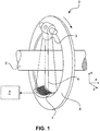
- Fig. 1 schematically and exemplarily illustrates a spectral or photon-counting radiation detector 1 which is capable of detecting individual incident x-ray photons and of determining their energies in accordance with predetermined energy ranges or bins.
- the radiation detector 1 is included in a computed tomography (CT) imaging device 2 for generating three-dimensional images of objects for medical or other purposes.
- CT computed tomography
- the radiation detector 1 may likewise be utilized in other applications than CT imaging.
- the CT imaging device 2 comprises an radiation source 3, such as an x-ray tube, that produces an x-ray beam 4 that traverses an examination region 5 between the radiation source 3 and the radiation detector 1, which comprises the object to be imaged.
- the x-ray radiation having traversed the examination region is collected by the radiation detector 1.
- the radiation detector 1 and the radiation source 3 may be mounted at opposing positions on a rotatable gantry 6 which can be rotated around the object positioned within the examination region 5. Moreover, the object and the gantry 6 can be moved relative to each other in the axial direction of the gantry 6 (z-direction).
- each projection corresponds to one angular position of the radiation source 3 and the radiation detector 1 relative to the object to be imaged, and by moving the object and the gantry 6 relative to each other in the z-direction, different so-called slices of the object can be imaged.
- the radiation detector 1 is coupled to a reconstruction unit 7 which reconstructs three-dimensional CT images on the basis of the measurement data collected by the radiation detector 1 and which may be configured as a computer device which comprises one or more processor units to execute computer programs implementing the routines carried out by the reconstruction unit 7.
- the measurement data provided by the radiation detector 1 are projections of the object, and images can be reconstructed from these projections in a way known to a person skilled in the art as such.
- the reconstruction unit 7 is capable of generating spectral CT images.
- the reconstruction unit 7 may generate sub-images for each energy bin. These sub-images may be further processed or evaluated separately, or the reconstruction unit 7 may combine the sub-images to form a combined image, e.g. on the basis of energy-dependent weighting of the sub-images.
- the reconstruction unit 7 may be configured to generate conventional CT images which do not include information derived from the photon energies.
- the reconstruction unit 7 may generate one or more spectral CT images, a conventional CT image or both spectral and conventional images, particularly depending on the intended further evaluation of the CT image(s).
- the radiation detector 1 is adapted to detect single incident x-ray photons and allows for determining their energies in accordance with a number of predefined energy bins.
- a photon incident into the radiation detector 1 produces an electric charge cloud of charge carriers (electrons and holes) which drift to the detector electrodes, where the amount of charge depends on the energy of the incident x-ray photon.
- the generated charges are collected by read-out electronics of the radiation detector 1, which in turn generate an electrical signal (e.g. a voltage signal) the amplitude of which is proportional to the energy of the impinging x-ray photon.
- the read-out electronics are capable of determining the photon energies.
- the read-out electronics are configured to determine the rate of incident photons as will be explained herein below.
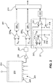
- the radiation detector 1 may comprise a plurality of detector elements 201, which are usually also referred to as tiles and which are preferably arranged in an array that may be flat or concave.
- the detector elements 201 are arranged in the form of rows and columns arranged substantially perpendicular to each other.
- each detector element 201 comprises a converter element 202 for converting X-rays into electrical signals, and read-out electronics coupled to the converter element 202.
- the read-out electronics may be implemented in a CMOS ASIC structure attached to the anode side of the converter element 202, for example
- the converter element 202 is provided between a cathode contact assembly 203 and an anode contact assembly 204 and is made of a semiconductor material.
- Suitable semiconductor materials include, for example, cadmium telluride (CdTe), cadmium zinc telluride (CdZnTe), cadmium tellurium selenide (CdTeSe), CdZnTeSe, cadmium manganese telluride (CdMnTe), silicon (Si), gallium arsenide (GaAs), perovskites and mercury iodide (HgI).
- the cathode contact assembly 203 is generally held on a lower electric potential than the anode contact assembly 204 (i.e.
- a negative bias voltage is applied to the cathode contact assembly 203 with respect to the anode contact assembly 204) so that an electric field is formed between the cathode contact assembly 203 and the anode contact assembly 204 within the converter element 202.
- X-ray photons may enter into the converter element 202 through the cathode contact assembly 203
- the converter element 202 may be configured as a substantially cubic block and its lateral dimensions may be much larger than its thickness.
- the cathode contact assembly 203 and the anode contact assembly 204 may be connected to the large top and bottom sides of the converter element 202 so that the electric field extends along the smaller thickness direction of the converter element 202.
- the cathode contact assembly 203 may be configured as a continuous cathode electrode, which may be formed by a thin metalized film applied onto the converter element 202.
- the anode contact assembly 204 may include pixelated anode electrodes 205, i.e. separated anode electrodes 205 which are arranged in certain distances to each other and which are usually also referred to as anode pixels.
- these anode pixels 205 are also arranged in rows and columns, which are substantially perpendicular to each other, on the surface of the conversion element 202.
- the anode electrodes or pixels 205 collect charge produced by photons incident on the converter element 202 and each anode pixel is connected to read-out electronics which collect the resulting current and determine the measurement data which are subsequently provided to the reconstruction unit 7.
- the read-out electronics may include an amplifier 206, such as a charge sensitive amplifier, which integrates the input current over each pulse (i.e. each incident x-ray photon) and produces a corresponding step-like output voltage signal, where the height of the step corresponds to the integrated charge and, thus, to the photon energy deposited in the converter element 202.
- the amplifier output signal is preferably filtered in a so-called pulse shaper circuit 207 to produce a voltage signal in which each step generated by the amplifier 206 corresponds to a pulse having a certain width and a gradually rounded maximum, the amplitude of which is proportional to the height of the step (i.e.
- the pulse shaper circuit 207 particularly sets the duration of the pulse.
- the pulse shaper circuit 207 limits the decay time of the step like output signal of the amplifier 206, which corresponds to a pulse having a very long decay time.
- the pulse shaper circuit 207 increases the rise time of the step-like amplifier output signal.
- the threshold values S i of these comparators 208 1 , ..., 208 N represent the boundaries of the aforementioned energy bins.
- a pulse in the output signal of the shaper circuit 207 which corresponds to a photon having an energy within a range corresponding to a certain energy bin, has an amplitude between the threshold values corresponding to the upper and lower boundaries for the energy bin.
- the corresponding configuration of the threshold values S i may be provided within the scope of a calibration procedure of the x-ray device 2, which may be carried out in a way known to the person skilled in the art as such.
- each comparator 208 1 , ..., 208 N may be connected to an associated counter 209 1 , ..., 209 N for counting the number of photons registered in the comparator 208 1 , ..., 208 N .
- each counter 209 1 , ..., 209 N may count the rising edges of the output signal of the associated comparator 208 1 , ..., 208 N .
- the read-out electronics may determine the rate of photon registrations (i.e. the number of photon registrations per unit time interval) for each energy bin.
- each detected photon produces a count with respect to the energy bin corresponding to its energy and with respect to the lower energy bins.
- the rate of detected photons within a certain energy bin can be determined on the basis of differences between the rates of photon registrations for the energy bins.
- the photon rate for the highest energy bin correspond to the number of registered photons with an energy in this energy bin.
- the number of registered photons with energies in a lower energy bin can determined on the basis of the differences between the number of photons with an energy in the next-higher bin and the counts for the respective energy bin.
- the detected rate of incident photons per energy bin can be determined. This determination may be made in the read-out electronics, and the determined rate information may be provided to the reconstruction unit 7 via a processing circuit 210 of the read-out electronics. As an alternative, the rates of photon registrations for each energy bin may be provided to the reconstruction unit 7, and the reconstruction unit 7 may determine the rate of photons per energy bin as explained above.
- the reconstruction unit 7 may reconstruct spectral images of the object positioned in the examination region 5 for each of the energy ranges corresponding to the energy bins. These images correspond to the aforementioned sub-images, which may be further evaluated separately or which may be combined to form a single x-ray image. Moreover, the reconstruction unit 7 can also generate conventional images on the basis of the number and/or rate information. For this purpose, the overall photon rate may be determined, which corresponds to the sum of the photon rates for all energy bins and the image is generated on the basis of this overall photon rate.
- the radiation detector 1 with the read-out electronics described above can reliably determine lower incident photon rates. However, photons may not be counted or associated with a wrong energy bin in case of higher incident photon rates. This affects both spectral and conventional CT image generation.
- the radiation detector 1 comprises a registration circuit 211 for registering incident photons independent of their energies and the aforementioned thresholds associated with the comparators 208 1 , ..., 208 N .
- the registration circuit provides an output signal which includes pulses at times at which the registration circuit 211 detects an incident photon.
- these pulses are relative narrow in order to avoid overlapping pulses in case of a high photon rate.
- the pulses are sufficiently broad to be reliable detected in the subsequent processing of the output signal of the registration circuit 211.
- the pulses of the output signal of the registration circuit 211 may be counted by means of a counter 212 in order to determine the overall number or rate of incident photons.
- the overall rate information may be output by the radiation detector 1 and provided to the reconstruction unit 7 in addition to the rate information for the energy bins determined by means of the counters 209 1 , ..., 209 N .
- the reconstruction unit 7 may generate conventional CT images in one embodiment. Spectral CT images may be generated on the basis of the rate information for the energy bins determined in the conventional way as explained above.
- the read-out electronics may determine the photon rate for the energy bins on the basis of the output signal provided by the registration circuit 211.
- the read-out electronics may assign each pulse of the output signal of the registration circuit 211 to one or more energy bins and may determine the photon rates for the energy bins on the basis of the number of pulses assigned to the energy bins.
- the read-out electronics may assign a pulse of the output signal of the registration circuit 211 to the highest energy bin associated with a comparator 208 1 , ..., 208 N that outputs a signal having a value larger than zero at the time at which the pulse occurs.
- this energy bin corresponds to the energy of the photon as determined on the basis of the output signal of the shaper circuit 207.
- the association may be determined in the processing circuit 210 of the read-out electronics on the basis of a corresponding algorithm implemented in the processing circuit 210.
- the read-out electronics can determine the number of incident photons for each energy bin and the corresponding photon rates for each energy bin.
- the counters 209 1 , ..., 209 N can be dispensed with for this determination.
- the determined rate information for the energy bins may be provided to the reconstruction unit 7 so that the reconstruction unit 7 can generate spectral CT images on the basis of this information.
- the radiation detector 1 may provide the overall rate information which may be determined using the counter 212 as explained above.
- the reconstruction unit 7 may generate conventional images.
- the reconstruction unit 7 may determine an overall rate information on the basis of the rate information for the individual energy bins in order to determine conventional images. In this case, the radiation detector 1 may not provide the overall rate information as an output signal in one implementation.
- the rate of photon events can be detected, which can be resolved by the conversion element 202, the amplifier 206 and the shaper circuit 207.
- the incident photon rate may exceed the resolution of the conversion element 202, the amplifier 206 and the shaper circuit 207.
- two or more photons arriving within a short time interval may produce a single pulse corresponding to the overall energy of the photons so that it is not possible to distinguish between distinct pulse peaks with respect to such photons.
- the photon rate determined on the basis of the signal provided by the registration circuit 211 and the counter 212 does not correspond to the true rate of incident photons, which is higher.
- the photon energies cannot be directly derived from ouptut of the comparators 208 1 , ..., 208 N in this case, since the photons produce a single pulse having an amplitude corresponding to a higher energy than the photon energies.
- the true rate of incident photons may be estimated by the read-out electronics of the radiation detector 1 or by the reconstruction unit on the basis of a model describing the response of the radiation detector 1 to an incident (high) photon flux.
- the true overall photon rate may be estimated in order to generate conventional x-ray images on the basis of this estimate and/or the true photon rates may be estimated for each energy bin in order to generate spectral images.
- the energies of the photons are estimated on the basis of the output signals of the comparators 208 1 , ..., 208 N . This estimation is made in addition to the estimation of the true photon rate using a correspondingly extended detector model which also takes the values of the amplitudes of the output signal of the shaper circuit 207 into consideration.
- the applied model may particularly describe the response of the registration circuit 211 and the counter 212 to an incident photon flux. Since the registration circuit registers incident photons independent of their energies, this response is a monotonic function of the incident flux. This allows for using a model with a relatively low complexity.
- One exemplary model, which may be used, is described in the publication E. Roessl et al., "On the analogy between pulse-pile up in energy sensitive, photon counting detectors and level-crossing of shot noise", Proc. SPIE 9783, Medical Imaging 2016: Physics of Medical Imaging, 97831H (25 March 2016); doi: 10.1117/12.2216909 .
- This publication discloses a model for the level crossing of a detector signal in response to an incident photon flux.
- This model can be applied to the response of the registration circuit 211 to an incident photon flux when considering the time derivative of the output signal of the shaper circuit 207 as the relevant detector signal and when considering a downward crossing of the value zero, since the registration circuit 211 effectively registers downward zero-crossings of this time derivative.
- the true incident photon rate may be estimated using the rate information determined on the basis of the signals provided by the registration circuit 211 and the counter 212 for the overall photon rate and/or the photon rates for the individual energy bins as explained above.
- the true energies of the photons may be estimated.
- the output signals of the comparators 208 1 , ..., 208 N may be taken into consideration and the model may be extended to describe the relationship between these output signals and the photon energies which are to be determined.
- the registration circuit 211 is configured as a maximum detector which is configured to detect local maxima of the output signal of the shaper circuit 207, and each detected local maximum is regarded as a photon event.
- the maximum detector may provide an output signal may comprise a narrow pulse at each occurrence of a local maximum of the output signal of the shaper circuit 207.
- the registration circuit 211 may comprises a peak holder circuit 213 which receives the output signal of the shaper circuit 207.
- the peak holder circuit 213 includes a capacitor 214, which is charged to the value of the output signal of the shaper circuit 207 when the voltage of the shaper circuit 207 increases and holds its charge for a certain amount of time when the value of the output signal of the shaper circuit 207 decreases.
- the actual value of the voltage across the capacitor is not evaluated in the registration circuit 211. This particularly means that the resistance of the capacitor 214 and the resulting charge leakage is substantially irrelevant.
- the capacitor 214 can therefore have a small capacitance, e.g. in the range of some femtofarad. Such a capacitor 214 can be charged and discharged quickly so that the capacitor voltage closely follows the value of the output signal of the shaper circuit 207.
- the output signal of the shaper circuit 207 may be fed to the non-inverting input of an operational amplifier 215, and the capacitor may be charged via the output of the operational amplifier and a further component.
- the capacitor voltage may further be provided to the inverting input of the operational amplifier 215 so that a closed loop is established.
- the operational amplifier 215 attempts to control its output such that the difference between voltages at the inputs, i.e. the value of the output signal of the shaper circuit 7 and the capacitor voltage, becomes zero.
- the further component is selected such that the output signal of the operational amplifier 215 effects a charging of the capacitor 214 when the value of the output signal of the shaper circuit 207 is larger than the capacitor voltage and that the output signal of the operational amplifier 215 does not change the capacitor voltage in case the value of the output signal of the shaper circuit 207 is smaller than the capacitor voltage.
- the further component is a transistor 216, particularly a junction gate field-effect transistor (JFET), via which the capacitor 214 is connected to a voltage source (V dd ).
- the output of the operational amplifier is connected to the gate contact of the transistor 216, and the transistor is configured such that the output signal of the operational amplifier 215 in case of a positive voltage difference at its inputs (i.e. in case the output signal of the shaper circuit 207 is larger than the capacitor voltage) controls the transistor 216 to be in a conductive state so that the capacitor 214 is charged and that the output signal of the operational amplifier 215 switches the transistor 216 off (so that it is not conducting) in case of a negative voltage difference at its inputs.
- JFET junction gate field-effect transistor
- the further component can be configured in a different way.
- the further component may be a diode and the output of the operational amplifier 215 may be connected to the capacitor 214 via the diode.
- the capacitor 214 can be charged via the output of the operational amplifier 214 in case of a positive voltage difference at its inputs and the diode can prevent discharging of the capacitor 214 in case of a negative voltage difference at the inputs of the operational amplifier 214.
- the registration circuit 211 of this embodiment comprises a comparator 217, which compares the value of the output signal of the shaper circuit 207 with the voltage across the capacitor 214.
- the comparator 217 may output a zero signal when the capacitor voltage is smaller than the value of the output signal of the shaper circuit 207.
- the comparator 217 outputs a signal larger than zero.
- the output signal of the comparator 217 also controls a switch 218 which can short-circuit the capacitor 214.
- the switch 218 is controlled such that it is closed (i.e. conductive) if the output signal of the comparator 217 is larger then zero and that it is open (i.e. non-conductive) otherwise.
- the capacitor 214 is discharged or "reset" when the output signal of the comparator 217 becomes larger then zero, i.e. when a local maximum of the output signal of the shaper circuit 207 is detected. Thereupon, the capacitor 214 can be charged again until the next local maximum of the output signal of the shaper circuit 207 occurs.
- the output signal of the comparator 217 becomes zero again (due to the discharged capacitor 214).
- the comparator 217 outputs a pulse at each occurrence of a local maximum of output signal of the shaper circuit 207.
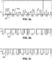
- Fig. 3a illustrates a sequence of 61 incident photons having an energy of 100 keV, where each photon event is illustrated by means of a pulse (one pulse is provided with the numeral 301). Further, Fig. 3a shows the output signal 302 of the shaper circuit 207 generated in response to the incident photons.
- the output signal of the shaper circuit 207 comprises pulses with a certain width, where each pulse corresponds to one incident photon or a number of incident photons which cannot be resolved in the conversion element 202, the integrating amplifier 206 and the shaper circuit 207 (due to the so-called pile-up effect) and, thus, are registered as a single event with a higher energy. Moreover, some of the pulses in the signal 302 overlap such that the signal 302 does not fall to zero between these pulses.
- Fig. 3b illustrates the output signal 303 of one of the comparators 208 1 , ..., 208 N , which compares the voltage of the signal 302 with a threshold value S corresponding to a photon energy of 25 keV.
- the signal 303 does not allow for distinguishing between photons when the signal 302 does not fall below the threshold between the pulses corresponding to such photons.
- Fig. 3c illustrates the output signal 304 of the registration circuit 211 which detects local maxima of the signal 302.
- Fig. 3c it is possible to detect all photons which can be resolved in the conversion element 202, the integrating amplifier 206 and the shaper circuit 207.
- a detector model may be used as explained above.
- the registration circuit 211 does not process the output signal of the shaper circuit 207 in order to determine the number of incident photons. Rather, the registration circuit 211 processes the output signal of the charge sensitive amplifier 206. As said above, this signal comprises a step at each photon event (where the height of the step is indicative of the photon energy). In order to evaluate this signal to detect photon events, the registration circuit 211 may be configured to detect such steps in the output signal of the charge senstive amplifier 206 and to output a narrow pulse (as in the embodiment described above) in case such a step is detected. To this end, the registration circuit 211 of this embodiment may comprise a capacitor, the voltage of which follows the value of the output signal of the integrating amplifier 206 with a certain small delay. A circuit comprising a comparator may compare the capacitor voltage with the value of the output signal of the integrating amplifier 206 in order to detect the steps and may produce a corresponding output signal.
- the output signal of the integrating amplifier 206 is less affected by processing delay compared with the output signal of the shaper circuit 207, the evaluation of the output signal of the integrating amplifier allows for a more accurate (i.e. faster) detection of the times at which the photons enter into the radiation detector 1.
- the output signal of the integrating amplifier 206 is usually more affected by noise so that there is increase of false detection when evaluating the output signal of the integrating amplifier 206.
- a computer program may be stored/distributed on a suitable medium, such as an optical storage medium or a solid-state medium, supplied together with or as part of other hardware, but may also be distributed in other forms, such as via the Internet or other wired or wireless telecommunication systems.
- a suitable medium such as an optical storage medium or a solid-state medium, supplied together with or as part of other hardware, but may also be distributed in other forms, such as via the Internet or other wired or wireless telecommunication systems.
Description
- The invention generally relates to spectral radiation detectors. More specifically, the invention relates to a radiation detector for detecting incident photons and to a method for detecting photons using the radiation detector.
- So-called spectral or photon-counting x-ray detectors allow for detecting incident x-ray photons individually and for determining their energies in accordance with predetermined energy bins (corresponding to certain energy ranges). For this purpose, the detectors comprises a direct conversion material which produces a pulse-like electric current signal each time a photon enters the material, where the current pulse corresponds to an amount of charge which is indicative of the photon energy. The current signals of successively arriving photons are processed in read-out electronics of the detector to produce an output signal comprising a pulse train in which each event (e.g. an incident photon) corresponds to a pulse having a certain width and an amplitude proportional to the energy of the incident photon.
- The pulses within the output signal can be detected and their amplitudes can be compared with threshold values in order to count the incident photons and determine the energy bins for these photons. To this end, circuitry may be associated with each energy bin, which includes a counter that is incremented when the output signal exceeds a threshold which corresponds to the lower boundary of the respective energy bin. On the basis of the counter outputs it is possible to determine the rate of incident photons per energy bin. This rate information may be provided to a reconstruction unit which generates x-ray images on the basis of this information.
- In the evaluation of the aforementioned output signal, a problem occurs when pulses for consecutive photons overlap in the output signal in such a way that the signal does not fall below one or more of the predetermined thresholds between the pulses. This is also known as pile-up. In case of pile-up, the pulses cannot be distinguished from each other and counted as one single pulse. This results in lost counts and corresponding artifacts in the generated images.
- Such artifacts impair the quality of spectral x-ray images, which are generated on the basis of the individual photon rates respectively determined for the energy bins. Moreover, photon-counting detectors can be used for generating conventional x-ray images independent of the determined energy information in certain applications. Such images may be generated on the basis of the overall photon rate determined for all energy bins (corresponding to the rate of photons producing a pulse in the output signal which is higher than the lowest threshold, i.e. the threshold corresponding to the lower boundary of the lowest energy bin). Also these images are affected by the lost counts.
-
WO 2008/146230 A2 discloses a photon-counting x-ray detector which comprises an amplifier/shaper circuit that produces a train of pulses on the basis of the signals produced by a detector element. The pulse train is evaluated in one or more photon counters that count pulses indicative of photons within certain energy bins on the basis of the pulse heights. Moreover, a local maximum detector detects local maxima in the pulse train and produces a count value indicative of the total number of photons received in the detector element. On the basis of this count value, the counts determined for the energy bins are adjusted, particularly in order to account for pulse pileup. -
WO 2008/146218 A2 relates to a photon-counting x-ray detector which has a slow shaper that produces pulses in response to incident photons, which are used for energy discrimination with respect to thresholds defining energy bins. Further, the detector comprises a fast shaper which generates pulses for energy discrimination with respect to the lowest energy threshold during a shortened integration interval. The signal generated in the fast shaper is processed in a comparator which outputs a signal that includes a rising edge each time the pulse amplitude of the signal from the fast shaper increases and crosses its threshold and a falling edge each time this signal decreases and crosses its threshold. The output signal of the comparator is fed to a pulse rejector, which produces a gating signal for gating off counters for counting the pulses associated with the energy bins in case the pulse rejector determines piled-up pulses. - It is an object of the present invention to improve a photon-counting radiation detector such that the number of lost counts is reduced by detecting local maxima of the output signal and to allow for an easy detection of such local maxima.
- In one aspect, the invention suggests a radiation detector for registering incident photons, comprising (i) detection circuitry configured to provide an electric output signal in response to incident photons, the output signal being a voltage signal comprising pulses having an amplitude indicative of energies deposited in the radiation detector by the incident photons, (ii) an energy estimating circuit configured to detect that the output signal is larger than at least one threshold corresponding to an energy value in order to determine energies of incident photons. The radiation detector further comprises a registration circuit configured to detect incident photons independent of a comparison of the output signal with the at least one threshold. The registration circuit comprises a maximum detector configured to detect and/or count local maxima of the output signal. The maximum detector comprises a peak detector circuit including a capacitor which is charged substantially to the value of the output signal, when the voltage of the signal increases and which holds its charge when the value of the output signal decreases, and the maximum detector includes a comparator circuit configured to detect a local maximum of the output signal when the value of the output signal falls below the voltage across the capacitor.
- The situation that the value of the output signal falls below the voltage across the capacitor occurs when the output signal decreases after the occurrence of a local maximum. Thus, the comparator can detect local maxima of the output signal by detecting such a situation. Since the radiation detector is configured to detect incident photons independent of a comparison with the at least one threshold on the basis of which the photon energies are determined, it is possible to detect incident photons without the drawbacks of the photon detection on the basis of this comparison. This allows for reducing the number of lost counts. By detecting local maxima of the output signal (instead of a crossing of a threshold) it is particularly possible to distinguish between pulses of the output signal, when these pulses overlap such that the output signal does not fall below a certain value between the pulses. Thus, incident photons producing such pulses in the output signal can be detected separately. In particular, each local maximum being detected and/or counted as an incident photon.
- One embodiment comprises that the capacitor is discharged when the value of the output signal falls below the voltage across the capacitor. This means that the capacitor is discharged or "reset" after the occurrence of a local maximum of the output signal. After having been discharged, the capacitor can be charged again as explained above in order to allow for the detection of the next local maximum of the output signal.
- In one embodiment, the detection circuitry comprises (i) a conversion element producing a pulse-like current signal in response to a photon incident onto the conversion element, (ii) an integrating amplifier coupled to the conversion element an producing a step-like signal portion in response to the pulse-like current signal and (iii) a shaper circuit configured to process the step-like signal portions to generate the aforementioned output signal. The registration circuit may detect incident photons on the basis of the output signal of the shaper circuit and oprtionally also on the basis of the output signal of the amplifier.
- When the registration circuit also detects incident photons on the basis of the output signal the integrating amplifier, the registration circuit may further be configured to detect and/or count step-like portions of the signal produced by the integrating amplifier as an incident photons. In this implementation, the output signal of the integration amplifier is used in addition to the aforementioned output signal of the shaper in order to detect incident photons. Usually, the output signal of the integrating amplifier allows for a faster detection of incident photons. However, it is more affected by noise.
- In one embodiment, the radiation detector is configured to output a number and/or rate of incident photons with respect to each of a plurality of predetermined photon energy ranges, the photon energy ranges being defined based on the at least one threshold. In a related embodiment, the radiation detector is configured to additionally output a number and/or rate of photons detected in the registration circuit.
- In a further related embodiment, the radiation detector is configured to determine the number and/or rate of incident photons with respect to each of the plurality of predetermined photon energy ranges on the basis of detections of photons in the registration circuit. In particular, the radiation detector maybe configured to determine the number and/or rate of incident photons with respect to one predetermined energy range on the basis of number of photons detected in the registration circuit while the output signal is larger than a threshold corresponding to a lower boundary of the energy range.
- In a further embodiment, the radiation detector is configured to assign a detected local maximum to an energy range pertaining to the highest threshold crossed by the output signal at the time of the detection of the local maximum and to detect a photon having an energy in said range based on the detection of the local maximum. For each threshold and each associated energy range an associated comparator may check whether the output signal exceeds the threshold. Thus, the local maximum may be assigned to the highest energy range associated with a comparator that outputs a signal having a value largher then zero at the time of the occurrence of the local maximum.
- In a further aspect, the invention suggests a method for detecting photons using a radiation detector as defined in
claim 1. The method comprises (i) receiving the electric output signal of the detection circuit, the output signal comprising pulses having an amplitude indicative of energies deposited in the radiation detector by the incident photons, (ii) detecting that the output signal is larger than at least one threshold corresponding to an energy value in order to determine energies of incident photons, and (iii) additionally detecting and/or counting incident photons independent of a comparison of the output signal with the at least one threshold in a registration cirucit, wherein a maximum detector of the registration circuit detects and/or counts local maxima of the output signal. The maximum detector comprises a peak detector circuit including a capacitor which is charged substantially to the value of the output signal, when the voltage of the signal increases and which holds its charge when the value of the output signal decreases, and a comparator circuit. The comparator circuit detects a local maximum of the output signal when the value of the output signal falls below the voltage across the capacitor. - It shall be understood that the radiation detector of
claim 1 and the method of claim 10 have similar and/or identical preferred embodiments, in particular, as defined in the dependent claims. - It shall be understood that a preferred embodiment of the present invention can also be any combination of the dependent claims or above embodiments with the respective independent claim.
- These and other aspects of the invention will be apparent from and elucidated with reference to the embodiments described hereinafter.
- In the following drawings:
-
Fig. 1 schematically and exemplarily shows a computed tomography imaging device comprising a radiation detector according to the invention, -
Fig. 2 schematically and exemplarily illustrates a detector element of radiation detector, and -
Figs. 3a-3c schematically and exemplarily illustrates results of a simulation of the operation of a detector element of the radiation detector. -
Fig. 1 schematically and exemplarily illustrates a spectral or photon-countingradiation detector 1 which is capable of detecting individual incident x-ray photons and of determining their energies in accordance with predetermined energy ranges or bins. In the illustrated embodiment, theradiation detector 1 is included in a computed tomography (CT)imaging device 2 for generating three-dimensional images of objects for medical or other purposes. However, theradiation detector 1 may likewise be utilized in other applications than CT imaging. - In addition to the x-ray-
detector 1, which will be explained in detail further below, theCT imaging device 2 comprises anradiation source 3, such as an x-ray tube, that produces anx-ray beam 4 that traverses anexamination region 5 between theradiation source 3 and theradiation detector 1, which comprises the object to be imaged. The x-ray radiation having traversed the examination region is collected by theradiation detector 1. Theradiation detector 1 and theradiation source 3 may be mounted at opposing positions on arotatable gantry 6 which can be rotated around the object positioned within theexamination region 5. Moreover, the object and thegantry 6 can be moved relative to each other in the axial direction of the gantry 6 (z-direction). Thus, different angular projections can be acquired when thegantry 6 is rotated around the object, where each projection corresponds to one angular position of theradiation source 3 and theradiation detector 1 relative to the object to be imaged, and by moving the object and thegantry 6 relative to each other in the z-direction, different so-called slices of the object can be imaged. - The
radiation detector 1 is coupled to areconstruction unit 7 which reconstructs three-dimensional CT images on the basis of the measurement data collected by theradiation detector 1 and which may be configured as a computer device which comprises one or more processor units to execute computer programs implementing the routines carried out by thereconstruction unit 7. The measurement data provided by theradiation detector 1 are projections of the object, and images can be reconstructed from these projections in a way known to a person skilled in the art as such. - Using the information about the energies of the photons detected by the
radiation detector 1, thereconstruction unit 7 is capable of generating spectral CT images. In so doing, thereconstruction unit 7 may generate sub-images for each energy bin. These sub-images may be further processed or evaluated separately, or thereconstruction unit 7 may combine the sub-images to form a combined image, e.g. on the basis of energy-dependent weighting of the sub-images. In addition, thereconstruction unit 7 may be configured to generate conventional CT images which do not include information derived from the photon energies. For each CT scan carried out with theCT device 2, thereconstruction unit 7 may generate one or more spectral CT images, a conventional CT image or both spectral and conventional images, particularly depending on the intended further evaluation of the CT image(s). - As said, the
radiation detector 1 is adapted to detect single incident x-ray photons and allows for determining their energies in accordance with a number of predefined energy bins. In this regard, a photon incident into theradiation detector 1 produces an electric charge cloud of charge carriers (electrons and holes) which drift to the detector electrodes, where the amount of charge depends on the energy of the incident x-ray photon. The generated charges are collected by read-out electronics of theradiation detector 1, which in turn generate an electrical signal (e.g. a voltage signal) the amplitude of which is proportional to the energy of the impinging x-ray photon. On this basis of this signal, the read-out electronics are capable of determining the photon energies. In addition, the read-out electronics are configured to determine the rate of incident photons as will be explained herein below. - More specifically, the
radiation detector 1 may comprise a plurality ofdetector elements 201, which are usually also referred to as tiles and which are preferably arranged in an array that may be flat or concave. Thus, thedetector elements 201 are arranged in the form of rows and columns arranged substantially perpendicular to each other. As schematically and exemplarily depicted inFig. 2 , eachdetector element 201 comprises aconverter element 202 for converting X-rays into electrical signals, and read-out electronics coupled to theconverter element 202. The read-out electronics may be implemented in a CMOS ASIC structure attached to the anode side of theconverter element 202, for example - The
converter element 202 is provided between acathode contact assembly 203 and ananode contact assembly 204 and is made of a semiconductor material. Suitable semiconductor materials include, for example, cadmium telluride (CdTe), cadmium zinc telluride (CdZnTe), cadmium tellurium selenide (CdTeSe), CdZnTeSe, cadmium manganese telluride (CdMnTe), silicon (Si), gallium arsenide (GaAs), perovskites and mercury iodide (HgI). In operation, thecathode contact assembly 203 is generally held on a lower electric potential than the anode contact assembly 204 (i.e. a negative bias voltage is applied to thecathode contact assembly 203 with respect to the anode contact assembly 204) so that an electric field is formed between thecathode contact assembly 203 and theanode contact assembly 204 within theconverter element 202. X-ray photons may enter into theconverter element 202 through thecathode contact assembly 203 - The
converter element 202 may be configured as a substantially cubic block and its lateral dimensions may be much larger than its thickness. Thecathode contact assembly 203 and theanode contact assembly 204 may be connected to the large top and bottom sides of theconverter element 202 so that the electric field extends along the smaller thickness direction of theconverter element 202. Further, thecathode contact assembly 203 may be configured as a continuous cathode electrode, which may be formed by a thin metalized film applied onto theconverter element 202. - In contrast, the
anode contact assembly 204 may includepixelated anode electrodes 205, i.e. separatedanode electrodes 205 which are arranged in certain distances to each other and which are usually also referred to as anode pixels. In one embodiment, theseanode pixels 205 are also arranged in rows and columns, which are substantially perpendicular to each other, on the surface of theconversion element 202. The anode electrodes orpixels 205 collect charge produced by photons incident on theconverter element 202 and each anode pixel is connected to read-out electronics which collect the resulting current and determine the measurement data which are subsequently provided to thereconstruction unit 7. - When an x-ray photon enters into the
converter element 202, it excites the semiconductor material and thereby generates electric charge carriers (electrons and holes). The negative charge carriers drift to one of theanode electrodes 205 under the influence of the electric field in theconverter element 202 and produce a pulse-like electric signal which is collected by the read-out electronics. - For each
anode electrode 205, the read-out electronics may include anamplifier 206, such as a charge sensitive amplifier, which integrates the input current over each pulse (i.e. each incident x-ray photon) and produces a corresponding step-like output voltage signal, where the height of the step corresponds to the integrated charge and, thus, to the photon energy deposited in theconverter element 202. The amplifier output signal is preferably filtered in a so-calledpulse shaper circuit 207 to produce a voltage signal in which each step generated by theamplifier 206 corresponds to a pulse having a certain width and a gradually rounded maximum, the amplitude of which is proportional to the height of the step (i.e. to the integrated charge of the charge cloud generated by an incident x-ray photon) and, thus, to the energy of the incident photon. For this purpose, thepulse shaper circuit 207 particularly sets the duration of the pulse. Thus, thepulse shaper circuit 207 limits the decay time of the step like output signal of theamplifier 206, which corresponds to a pulse having a very long decay time. In addition, thepulse shaper circuit 207 increases the rise time of the step-like amplifier output signal. - Further, the read-out electronics comprise two or more comparators 2081, ..., 208N, where each comparators 2081, ..., 208N compares the output signal of the
shaper circuit 207 with an associated predetermined threshold value Si (i = 1,...,N) and produces an output signal greater than zero, (only) if the output of theshaper circuit 207 exceeds the threshold value Si. The threshold values Si of these comparators 2081, ..., 208N represent the boundaries of the aforementioned energy bins. They may be selected such that a pulse in the output signal of theshaper circuit 207, which corresponds to a photon having an energy within a range corresponding to a certain energy bin, has an amplitude between the threshold values corresponding to the upper and lower boundaries for the energy bin. The corresponding configuration of the threshold values Si may be provided within the scope of a calibration procedure of thex-ray device 2, which may be carried out in a way known to the person skilled in the art as such. - Conventionally, the output of each comparator 2081, ..., 208N may be connected to an associated
counter 2091, ..., 209N for counting the number of photons registered in the comparator 2081, ..., 208N. To this end, eachcounter 2091, ..., 209N may count the rising edges of the output signal of the associated comparator 2081, ..., 208N. On the basis of the counted number of photons, the read-out electronics may determine the rate of photon registrations (i.e. the number of photon registrations per unit time interval) for each energy bin. - In accordance with this configuration, each detected photon produces a count with respect to the energy bin corresponding to its energy and with respect to the lower energy bins. Thus, the rate of detected photons within a certain energy bin can be determined on the basis of differences between the rates of photon registrations for the energy bins. In particular, the photon rate for the highest energy bin correspond to the number of registered photons with an energy in this energy bin. The number of registered photons with energies in a lower energy bin can determined on the basis of the differences between the number of photons with an energy in the next-higher bin and the counts for the respective energy bin.
- In such a way, the detected rate of incident photons per energy bin can be determined. This determination may be made in the read-out electronics, and the determined rate information may be provided to the
reconstruction unit 7 via aprocessing circuit 210 of the read-out electronics. As an alternative, the rates of photon registrations for each energy bin may be provided to thereconstruction unit 7, and thereconstruction unit 7 may determine the rate of photons per energy bin as explained above. - On the basis of the photon rate per energy bin, the
reconstruction unit 7 may reconstruct spectral images of the object positioned in theexamination region 5 for each of the energy ranges corresponding to the energy bins. These images correspond to the aforementioned sub-images, which may be further evaluated separately or which may be combined to form a single x-ray image. Moreover, thereconstruction unit 7 can also generate conventional images on the basis of the number and/or rate information. For this purpose, the overall photon rate may be determined, which corresponds to the sum of the photon rates for all energy bins and the image is generated on the basis of this overall photon rate. - The
radiation detector 1 with the read-out electronics described above can reliably determine lower incident photon rates. However, photons may not be counted or associated with a wrong energy bin in case of higher incident photon rates. This affects both spectral and conventional CT image generation. - One reason for such lost or incorrectly classified counts is that individual photons are only registered by each of the
counters 2091, ..., 209N when the output signal of theshaper circuit 207 crosses the threshold assigned to the relevant comparator 2081, ..., 208N from a value below the threshold to a value above the threshold. Thus, a registration of a photon in thecounters 2091, ..., 209N (with a correct energy) requires that the output signal of theshaper circuit 207 falls to zero or at least below the lowest threshold between two pulses corresponding to consecutive incident photons. This may not be the case for higher photon rates even if theconversion element 202, theamplifier 206 and theshaper 207 can resolve consecutive photons (i.e. if the output signal of theshaper 207 comprises distinct peaks corresponding to the photons), since the pulses in the output signal of theshaper 207 may overlap such that the signal does not fall below the relevant threshold(s) between the pulses. - In order to solve this problem, the
radiation detector 1 comprises aregistration circuit 211 for registering incident photons independent of their energies and the aforementioned thresholds associated with the comparators 2081, ..., 208N. In one implementation, the registration circuit provides an output signal which includes pulses at times at which theregistration circuit 211 detects an incident photon. Preferably, these pulses are relative narrow in order to avoid overlapping pulses in case of a high photon rate. On the other hand, the pulses are sufficiently broad to be reliable detected in the subsequent processing of the output signal of theregistration circuit 211. - In this regard, the pulses of the output signal of the
registration circuit 211 may be counted by means of acounter 212 in order to determine the overall number or rate of incident photons. In this case, the overall rate information may be output by theradiation detector 1 and provided to thereconstruction unit 7 in addition to the rate information for the energy bins determined by means of thecounters 2091, ..., 209N. Using only the addition overall rate information thereconstruction unit 7 may generate conventional CT images in one embodiment. Spectral CT images may be generated on the basis of the rate information for the energy bins determined in the conventional way as explained above. - In a further embodiment, the read-out electronics may determine the photon rate for the energy bins on the basis of the output signal provided by the
registration circuit 211. In particular, the read-out electronics may assign each pulse of the output signal of theregistration circuit 211 to one or more energy bins and may determine the photon rates for the energy bins on the basis of the number of pulses assigned to the energy bins. In so doing, the read-out electronics may assign a pulse of the output signal of theregistration circuit 211 to the highest energy bin associated with a comparator 2081, ..., 208N that outputs a signal having a value larger than zero at the time at which the pulse occurs. As will be apparent from the description above, this energy bin corresponds to the energy of the photon as determined on the basis of the output signal of theshaper circuit 207. The association may be determined in theprocessing circuit 210 of the read-out electronics on the basis of a corresponding algorithm implemented in theprocessing circuit 210. When the association is made for each pulse of the output signal of the registration circuit 211 (i.e. for each registered photon), the read-out electronics can determine the number of incident photons for each energy bin and the corresponding photon rates for each energy bin. Thecounters 2091, ..., 209N can be dispensed with for this determination. - The determined rate information for the energy bins may be provided to the
reconstruction unit 7 so that thereconstruction unit 7 can generate spectral CT images on the basis of this information. In addition, theradiation detector 1 may provide the overall rate information which may be determined using thecounter 212 as explained above. On the basis of the overall rate information, thereconstruction unit 7 may generate conventional images. Likewise, thereconstruction unit 7 may determine an overall rate information on the basis of the rate information for the individual energy bins in order to determine conventional images. In this case, theradiation detector 1 may not provide the overall rate information as an output signal in one implementation. - Using the rate information determined on the basis of the signals provided by the
registration circuit 211 and thecounter 212, the rate of photon events can be detected, which can be resolved by theconversion element 202, theamplifier 206 and theshaper circuit 207. However, the incident photon rate may exceed the resolution of theconversion element 202, theamplifier 206 and theshaper circuit 207. In particular, two or more photons arriving within a short time interval may produce a single pulse corresponding to the overall energy of the photons so that it is not possible to distinguish between distinct pulse peaks with respect to such photons. In this case, the photon rate determined on the basis of the signal provided by theregistration circuit 211 and thecounter 212 does not correspond to the true rate of incident photons, which is higher. Moreover, the photon energies cannot be directly derived from ouptut of the comparators 2081, ..., 208N in this case, since the photons produce a single pulse having an amplitude corresponding to a higher energy than the photon energies. - In order to be able to generate accurate conventional and/or spectral images in this case, the true rate of incident photons may be estimated by the read-out electronics of the
radiation detector 1 or by the reconstruction unit on the basis of a model describing the response of theradiation detector 1 to an incident (high) photon flux. Using such a detector model, the true overall photon rate may be estimated in order to generate conventional x-ray images on the basis of this estimate and/or the true photon rates may be estimated for each energy bin in order to generate spectral images. In order to estimate the true photon rates for the energy bins, the energies of the photons are estimated on the basis of the output signals of the comparators 2081, ..., 208N. This estimation is made in addition to the estimation of the true photon rate using a correspondingly extended detector model which also takes the values of the amplitudes of the output signal of theshaper circuit 207 into consideration. - In order to determine the true photon rate, the applied model may particularly describe the response of the
registration circuit 211 and thecounter 212 to an incident photon flux. Since the registration circuit registers incident photons independent of their energies, this response is a monotonic function of the incident flux. This allows for using a model with a relatively low complexity. One exemplary model, which may be used, is described in the publication E. Roessl et al., "On the analogy between pulse-pile up in energy sensitive, photon counting detectors and level-crossing of shot noise", Proc. SPIE 9783, Medical Imaging 2016: Physics of Medical Imaging, 97831H (25 March 2016); doi: 10.1117/12.2216909. This publication discloses a model for the level crossing of a detector signal in response to an incident photon flux. This model can be applied to the response of theregistration circuit 211 to an incident photon flux when considering the time derivative of the output signal of theshaper circuit 207 as the relevant detector signal and when considering a downward crossing of the value zero, since theregistration circuit 211 effectively registers downward zero-crossings of this time derivative. - Using such a model, the true incident photon rate may be estimated using the rate information determined on the basis of the signals provided by the
registration circuit 211 and thecounter 212 for the overall photon rate and/or the photon rates for the individual energy bins as explained above. In addition the true energies of the photons may be estimated. For this purpose, the output signals of the comparators 2081, ..., 208N may be taken into consideration and the model may be extended to describe the relationship between these output signals and the photon energies which are to be determined. - In one embodiment, the
registration circuit 211 is configured as a maximum detector which is configured to detect local maxima of the output signal of theshaper circuit 207, and each detected local maximum is regarded as a photon event. In order to further evaluate the detection of maxima as explained above, the maximum detector may provide an output signal may comprise a narrow pulse at each occurrence of a local maximum of the output signal of theshaper circuit 207. - In one implementation of this embodiment, which is schematically and exemplarily illustrated in
Fig. 2 , theregistration circuit 211 may comprises apeak holder circuit 213 which receives the output signal of theshaper circuit 207. Thepeak holder circuit 213 includes acapacitor 214, which is charged to the value of the output signal of theshaper circuit 207 when the voltage of theshaper circuit 207 increases and holds its charge for a certain amount of time when the value of the output signal of theshaper circuit 207 decreases. As will become apparent from the following description, the actual value of the voltage across the capacitor is not evaluated in theregistration circuit 211. This particularly means that the resistance of thecapacitor 214 and the resulting charge leakage is substantially irrelevant. Thecapacitor 214 can therefore have a small capacitance, e.g. in the range of some femtofarad. Such acapacitor 214 can be charged and discharged quickly so that the capacitor voltage closely follows the value of the output signal of theshaper circuit 207. - In order to charge the
capacitor 214, the output signal of theshaper circuit 207 may be fed to the non-inverting input of anoperational amplifier 215, and the capacitor may be charged via the output of the operational amplifier and a further component. The capacitor voltage may further be provided to the inverting input of theoperational amplifier 215 so that a closed loop is established. In such a configuration, theoperational amplifier 215 attempts to control its output such that the difference between voltages at the inputs, i.e. the value of the output signal of theshaper circuit 7 and the capacitor voltage, becomes zero. The further component is selected such that the output signal of theoperational amplifier 215 effects a charging of thecapacitor 214 when the value of the output signal of theshaper circuit 207 is larger than the capacitor voltage and that the output signal of theoperational amplifier 215 does not change the capacitor voltage in case the value of the output signal of theshaper circuit 207 is smaller than the capacitor voltage. - In the implementation illustrated in
Fig. 2 , the further component is a transistor 216, particularly a junction gate field-effect transistor (JFET), via which thecapacitor 214 is connected to a voltage source (Vdd). The output of the operational amplifier is connected to the gate contact of the transistor 216, and the transistor is configured such that the output signal of theoperational amplifier 215 in case of a positive voltage difference at its inputs (i.e. in case the output signal of theshaper circuit 207 is larger than the capacitor voltage) controls the transistor 216 to be in a conductive state so that thecapacitor 214 is charged and that the output signal of theoperational amplifier 215 switches the transistor 216 off (so that it is not conducting) in case of a negative voltage difference at its inputs. - In further possible implementations, the further component can be configured in a different way. For instance, the further component may be a diode and the output of the
operational amplifier 215 may be connected to thecapacitor 214 via the diode. Thus, thecapacitor 214 can be charged via the output of theoperational amplifier 214 in case of a positive voltage difference at its inputs and the diode can prevent discharging of thecapacitor 214 in case of a negative voltage difference at the inputs of theoperational amplifier 214. - In addition, the
registration circuit 211 of this embodiment comprises acomparator 217, which compares the value of the output signal of theshaper circuit 207 with the voltage across thecapacitor 214. Thecomparator 217 may output a zero signal when the capacitor voltage is smaller than the value of the output signal of theshaper circuit 207. When the capacitor voltage is larger than the value of the output signal of the shaper circuit 207 (i.e. when the voltage output signal begins to decrease after occurrence of a local maximum), thecomparator 217 outputs a signal larger than zero. - The output signal of the
comparator 217 also controls aswitch 218 which can short-circuit thecapacitor 214. Theswitch 218 is controlled such that it is closed (i.e. conductive) if the output signal of thecomparator 217 is larger then zero and that it is open (i.e. non-conductive) otherwise. Thus, thecapacitor 214 is discharged or "reset" when the output signal of thecomparator 217 becomes larger then zero, i.e. when a local maximum of the output signal of theshaper circuit 207 is detected. Thereupon, thecapacitor 214 can be charged again until the next local maximum of the output signal of theshaper circuit 207 occurs. Moreover, the output signal of thecomparator 217 becomes zero again (due to the discharged capacitor 214). - Thus, the
comparator 217 outputs a pulse at each occurrence of a local maximum of output signal of theshaper circuit 207. - In
Figs. 3a-3c , results of a simulation of the operation of the read-out electronics comprising aregistration circuit 211 in the aforementioned embodiment are schematically and exemplarily illustrated. -
Fig. 3a illustrates a sequence of 61 incident photons having an energy of 100 keV, where each photon event is illustrated by means of a pulse (one pulse is provided with the numeral 301). Further,Fig. 3a shows theoutput signal 302 of theshaper circuit 207 generated in response to the incident photons. As can be seen inFig. 3a , the output signal of theshaper circuit 207 comprises pulses with a certain width, where each pulse corresponds to one incident photon or a number of incident photons which cannot be resolved in theconversion element 202, the integratingamplifier 206 and the shaper circuit 207 (due to the so-called pile-up effect) and, thus, are registered as a single event with a higher energy. Moreover, some of the pulses in thesignal 302 overlap such that thesignal 302 does not fall to zero between these pulses. -
Fig. 3b illustrates theoutput signal 303 of one of the comparators 2081, ..., 208N, which compares the voltage of thesignal 302 with a threshold value S corresponding to a photon energy of 25 keV. As can be seen inFig. 3b , thesignal 303 does not allow for distinguishing between photons when thesignal 302 does not fall below the threshold between the pulses corresponding to such photons. As a result, it is possible to detect 13 photon events, and it is not possible to detect all photon events which can be resolved by theconversion element 202, the integratingamplifier 206 and the shaper circuit 207 (i.e. which produce a local maximum of the signal 302). -
Fig. 3c illustrates theoutput signal 304 of theregistration circuit 211 which detects local maxima of thesignal 302. As can be seen inFig. 3c , it is possible to detect all photons which can be resolved in theconversion element 202, the integratingamplifier 206 and theshaper circuit 207. For the sequence of photons shown inFig. 3a , this means that it is possible to detect 26 photon events. Thus, it is possible to detect significantly more photons on the basis of theoutput signal 304 of theregistration circuit 211 than on the basis of theoutput signal 303 of the comparator 2081, ... , 208N. In order to estimate the true number of incident photons (61 in the example shown inFig. 3 ) a detector model may be used as explained above. - In a further embodiment, the
registration circuit 211 does not process the output signal of theshaper circuit 207 in order to determine the number of incident photons. Rather, theregistration circuit 211 processes the output signal of the chargesensitive amplifier 206. As said above, this signal comprises a step at each photon event (where the height of the step is indicative of the photon energy). In order to evaluate this signal to detect photon events, theregistration circuit 211 may be configured to detect such steps in the output signal of the charge senstiveamplifier 206 and to output a narrow pulse (as in the embodiment described above) in case such a step is detected. To this end, theregistration circuit 211 of this embodiment may comprise a capacitor, the voltage of which follows the value of the output signal of the integratingamplifier 206 with a certain small delay. A circuit comprising a comparator may compare the capacitor voltage with the value of the output signal of the integratingamplifier 206 in order to detect the steps and may produce a corresponding output signal. - Since the output signal of the integrating
amplifier 206 is less affected by processing delay compared with the output signal of theshaper circuit 207, the evaluation of the output signal of the integrating amplifier allows for a more accurate (i.e. faster) detection of the times at which the photons enter into theradiation detector 1. However, the output signal of the integratingamplifier 206 is usually more affected by noise so that there is increase of false detection when evaluating the output signal of the integratingamplifier 206. - Other variations to the disclosed embodiments can be understood and effected by those skilled in the art in practicing the claimed invention, from a study of the drawings, the disclosure, and the appended claims.
- In the claims, the word "comprising" does not exclude other elements or steps, and the indefinite article "a" or "an" does not exclude a plurality.
- A computer program may be stored/distributed on a suitable medium, such as an optical storage medium or a solid-state medium, supplied together with or as part of other hardware, but may also be distributed in other forms, such as via the Internet or other wired or wireless telecommunication systems.
- Any reference signs in the claims should not be construed as limiting the scope.
Claims (10)
- A radiation detector (1) for registering incident photons, comprising:- detection circuitry (202, 206, 207) configured to provide an electric output signal in response to incident photons, the output signal being a voltage signal comprising pulses having an amplitude indicative of energies deposited in the radiation detector by the incident photons,- an energy estimating circuit (2081, ..., 208N; 2091, ..., 209N) configured to detect that the output signal is larger than at least one threshold corresponding to an energy value in order to determine energies of incident photons, anda registration circuit (211) configured to detect incident photons independent of a comparison of the output signal with the at least one threshold,
wherein the registration circuit (211) comprises a maximum detector (213, 217, 218) configured to detect and/or count local maxima of the output signal,
the maximum detector (213, 217, 218) comprising a peak detector circuit (213) including a capacitor (214) which is charged substantially to the value of the output signal, when the voltage of the signal increases and which holds its charge when the value of the output signal decreases, and
the maximum detector (213, 217, 218) including a comparator circuit (217) configured to detect a local maximum of the output signal when the value of the output signal falls below the voltage across the capacitor (214). - The radiation detector (1) as defined in claim 1, wherein the capacitor (214) is discharged when the value of the output signal falls below the voltage across the capacitor (214).
- The radiation detector (1) as defined in claim 1, wherein the detection circuitry (202, 206, 207) comprises:- a conversion element (202) producing a pulse-like current signal in response to a photon incident onto the conversion element (202),- an integrating amplifier (206) coupled to the conversion element (202) and producing a step-like signal portions in response to the pulse-like current signal, and- a shaper circuit (207) configured to process the step-like signal portions to generate the output signal.
- The radiation detector (1) as defined in claim 3, wherein the registration circuit is further configured to detect and/or count step-like portions of the signal produced by the integrating amplifier (206) as an incident photons.
- The radiation detector (1) as defined in claim 1, being configured to output a number and/or rate of incident photons with respect to each of a plurality of predetermined photon energy ranges, the photon energy ranges being defined based on the at least one threshold.
- The radiation detector (1) as defined in claim 5, being configured to additionally output a number and/or rate of photons detected in the registration circuit (211).
- The radiation detector (1) as defined in claim 5, being configured to determine the number and/or rate of incident photons with respect to each of the plurality of predetermined photon energy ranges on the basis of detections of photons in the registration circuit (211).
- The radiation detector (1) as defined in claim 7, being configured to determine the number and/or rate of incident photons with respect to one predetermined energy range on the basis of number of photons detected in the registration circuit (211) while the output signal is larger than a threshold corresponding to a lower boundary of the energy range.
- The radiation detector as defined in claim 1, being configured to assign a detected local maximum to an energy range pertaining to the highest threshold crossed by the output signal at the time of the detection of the local maximum and to detect a photon having an energy in said range based on the detection of the local maximum.
- A method for detecting photons using a radiation detector (1) as defined in claim 1, the method comprising:- receiving the electric output signal of the detection circuit (202, 206, 207), the output signal being a voltage signal comprising pulses having an amplitude indicative of energies deposited in the radiation detector by the incident photons,- detecting that the output signal is larger than at least one threshold corresponding to an energy value in order to determine energies of incident photons,- additionally detecting and/or counting incident photons independent of a comparison of the output signal with the at least one threshold in a registration cirucit (211),wherein a maximum detector (213, 217, 218) of the registration circuit (211) detects and/or counts local maxima of the output signal, and
wherein the maximum detector (213, 217, 218) comprises a peak detector circuit (213) including a capacitor (214) which is charged substantially to the value of the output signal, when the voltage of the signal increases and which holds its charge when the value of the output signal decreases, and a comparator circuit (217),
the comparator circuit (217) detecting a local maximum of the output signal when the value of the output signal falls below the voltage across the capacitor (214).
Applications Claiming Priority (2)
| Application Number | Priority Date | Filing Date | Title |
|---|---|---|---|
| EP16174692 | 2016-06-16 | ||
| PCT/EP2017/064838 WO2017216378A1 (en) | 2016-06-16 | 2017-06-16 | Improved photon-counting in a spectral radiation detector |
Publications (2)
| Publication Number | Publication Date |
|---|---|
| EP3472647A1 EP3472647A1 (en) | 2019-04-24 |
| EP3472647B1 true EP3472647B1 (en) | 2020-08-05 |
Family
ID=56132829
Family Applications (1)
| Application Number | Title | Priority Date | Filing Date |
|---|---|---|---|
| EP17729512.8A Active EP3472647B1 (en) | 2016-06-16 | 2017-06-16 | Improved photon-counting in a spectral radiation detector |
Country Status (5)
| Country | Link |
|---|---|
| US (1) | US11029425B2 (en) |
| EP (1) | EP3472647B1 (en) |
| JP (1) | JP7041079B6 (en) |
| CN (1) | CN109477903B (en) |
| WO (1) | WO2017216378A1 (en) |
Families Citing this family (7)
| Publication number | Priority date | Publication date | Assignee | Title |
|---|---|---|---|---|
| WO2019113440A1 (en) * | 2017-12-08 | 2019-06-13 | Rensselaer Polytechnic Institute | A neural network-based corrector for photon counting detectors |
| EP3611542A1 (en) * | 2018-08-13 | 2020-02-19 | STMicroelectronics (Research & Development) Limited | Proximity sensor and method of operating a photodetector based proximity sensor |
| US11105938B2 (en) * | 2019-06-12 | 2021-08-31 | Redlen Technologies, Inc. | Time signatures and pattern matching in x-ray photon counting detectors |
| CN110389374B (en) * | 2019-07-05 | 2020-10-30 | 东软医疗系统股份有限公司 | Front-end circuit of detector and detector |
| CN110456404B (en) * | 2019-08-14 | 2023-07-28 | 苏州瑞迈斯科技有限公司 | Radiation detection device and imaging system |
| CN110412644A (en) * | 2019-08-14 | 2019-11-05 | 苏州瑞迈斯医疗科技有限公司 | Photoncounting methods and device |
| CN114114375B (en) * | 2021-11-22 | 2023-06-13 | 核工业西南物理研究院 | Plasma hot electron measurement system and measurement method |
Family Cites Families (21)
| Publication number | Priority date | Publication date | Assignee | Title |
|---|---|---|---|---|
| US7818047B2 (en) * | 2001-11-09 | 2010-10-19 | Nova R&D, Inc. | X-ray and gamma ray detector readout system |
| JP4895161B2 (en) | 2005-10-31 | 2012-03-14 | 横河電機株式会社 | Peak detection circuit and radiation measurement device |
| US7829860B2 (en) * | 2006-10-31 | 2010-11-09 | Dxray, Inc. | Photon counting imaging detector system |
| WO2008146230A2 (en) | 2007-05-29 | 2008-12-04 | Koninklijke Philips Electronics N.V. | Photon counting with detection of local maxima |
| EP2156218A2 (en) * | 2007-06-01 | 2010-02-24 | Koninklijke Philips Electronics N.V. | Spectral photon counting detector |
| CN101680955A (en) * | 2007-06-19 | 2010-03-24 | 皇家飞利浦电子股份有限公司 | spectral photon counting detector |
| US8338791B2 (en) * | 2007-06-19 | 2012-12-25 | Koninklijke Philips Electronics N.V. | Digital pulse processing for multi-spectral photon counting readout circuits |
| CN102016637A (en) * | 2008-04-30 | 2011-04-13 | 皇家飞利浦电子股份有限公司 | Counting detector |
| US8269180B2 (en) * | 2008-08-27 | 2012-09-18 | Brookhaven Science Associates, Llc | Method and apparatus for the measurement of signals from radiation sensors |
| US8440957B2 (en) * | 2009-02-25 | 2013-05-14 | Bart Dierickx | Counting pixel with good dynamic range properties |
| DE102009018995B4 (en) * | 2009-04-27 | 2017-10-12 | Siemens Healthcare Gmbh | Method and circuit for determining an intensity of ionizing radiation |
| US9310495B2 (en) * | 2011-05-04 | 2016-04-12 | Oy Ajat Ltd. | Photon/energy identifying X-ray and gamma ray imaging device (“PID”) with a two dimensional array of pixels and system therefrom |
| DE102011076781B4 (en) * | 2011-05-31 | 2018-05-03 | Siemens Healthcare Gmbh | Method for correcting a counting rate drift in a quantum-counting detector, X-ray system with quantum-counting detector and circuit arrangement for a quantum-counting detector |
| WO2013073071A1 (en) | 2011-11-15 | 2013-05-23 | 富士電機株式会社 | Pulse processing device and radiation analysis apparatus |
| RU2015102321A (en) | 2012-06-27 | 2016-08-10 | Конинклейке Филипс Н.В. | SPECTRAL DETECTOR FOR PHOTON COUNTING |
| DE102012212124B4 (en) * | 2012-07-11 | 2018-06-14 | Siemens Healthcare Gmbh | Counting digital x-ray detector and method of capturing a series of x-ray images |
| JP6301138B2 (en) * | 2013-02-12 | 2018-03-28 | キヤノンメディカルシステムズ株式会社 | X-ray computed tomography apparatus and photon counting program |
| WO2014173812A1 (en) * | 2013-04-24 | 2014-10-30 | Koninklijke Philips N.V. | Pulse processing circuit with correction means |
| JP2016032635A (en) * | 2014-07-30 | 2016-03-10 | 株式会社東芝 | Photon-counting type x-ray ct apparatus |
| DE102015205301A1 (en) * | 2015-03-24 | 2016-09-29 | Siemens Healthcare Gmbh | Operating a counting digital x-ray image detector |
| US9851460B1 (en) * | 2016-09-07 | 2017-12-26 | Toshiba Medical Systmes Corporation | Apparatus and method for a high-flux photon-counting spectral application-specific integrated circuit (ASIC) having a charge summing mode |
-
2017
- 2017-06-16 CN CN201780036746.XA patent/CN109477903B/en active Active
- 2017-06-16 US US16/305,425 patent/US11029425B2/en active Active
- 2017-06-16 EP EP17729512.8A patent/EP3472647B1/en active Active
- 2017-06-16 JP JP2018565402A patent/JP7041079B6/en active Active
- 2017-06-16 WO PCT/EP2017/064838 patent/WO2017216378A1/en unknown
Non-Patent Citations (1)
| Title |
|---|
| None * |
Also Published As
| Publication number | Publication date |
|---|---|
| EP3472647A1 (en) | 2019-04-24 |
| JP7041079B2 (en) | 2022-03-23 |
| CN109477903B (en) | 2023-08-04 |
| US20200326437A1 (en) | 2020-10-15 |
| JP7041079B6 (en) | 2022-05-30 |
| JP2019521335A (en) | 2019-07-25 |
| WO2017216378A1 (en) | 2017-12-21 |
| CN109477903A (en) | 2019-03-15 |
| US11029425B2 (en) | 2021-06-08 |
Similar Documents
| Publication | Publication Date | Title |
|---|---|---|
| EP3472647B1 (en) | Improved photon-counting in a spectral radiation detector | |
| EP3074791B1 (en) | Detection device for detecting photons and method therefor | |
| US9677931B2 (en) | Detection of radiation quanta using an optical detector pixel array and pixel cell trigger state sensing circuits | |
| US10575800B2 (en) | Increased spatial resolution for photon-counting edge-on x-ray detectors | |
| JP5860590B2 (en) | Radiation monitoring device | |
| CN110462442B (en) | Photon counting detector for realizing coincidence | |
| JP2015516830A (en) | High magnetic flux photon counting detector | |
| CN109313275B (en) | Dead Time Calibration for Radiation Detectors | |
| CN108293096B (en) | Radiation detector and x-ray imaging system | |
| EP3234651B1 (en) | Baseline shift determination for a photon detector | |
| EP3973330B1 (en) | X-ray and gamma imaging using a single radiation detector | |
| US20220167936A1 (en) | Methods and systems for coincidence detection in x-ray detectors | |
| JP2023510155A (en) | Compensation for polarization effects in photon counting detectors |
Legal Events
| Date | Code | Title | Description |
|---|---|---|---|
| STAA | Information on the status of an ep patent application or granted ep patent |
Free format text: STATUS: UNKNOWN |
|
| STAA | Information on the status of an ep patent application or granted ep patent |
Free format text: STATUS: THE INTERNATIONAL PUBLICATION HAS BEEN MADE |
|
| PUAI | Public reference made under article 153(3) epc to a published international application that has entered the european phase |
Free format text: ORIGINAL CODE: 0009012 |
|
| STAA | Information on the status of an ep patent application or granted ep patent |
Free format text: STATUS: REQUEST FOR EXAMINATION WAS MADE |
|
| 17P | Request for examination filed |
Effective date: 20190116 |
|
| AK | Designated contracting states |
Kind code of ref document: A1 Designated state(s): AL AT BE BG CH CY CZ DE DK EE ES FI FR GB GR HR HU IE IS IT LI LT LU LV MC MK MT NL NO PL PT RO RS SE SI SK SM TR |
|
| AX | Request for extension of the european patent |
Extension state: BA ME |
|
| DAV | Request for validation of the european patent (deleted) | ||
| DAX | Request for extension of the european patent (deleted) | ||
| GRAP | Despatch of communication of intention to grant a patent |
Free format text: ORIGINAL CODE: EPIDOSNIGR1 |
|
| STAA | Information on the status of an ep patent application or granted ep patent |
Free format text: STATUS: GRANT OF PATENT IS INTENDED |
|
| INTG | Intention to grant announced |
Effective date: 20200205 |
|
| RAP1 | Party data changed (applicant data changed or rights of an application transferred) |
Owner name: KONINKLIJKE PHILIPS N.V. |
|
| GRAS | Grant fee paid |
Free format text: ORIGINAL CODE: EPIDOSNIGR3 |
|
| GRAA | (expected) grant |
Free format text: ORIGINAL CODE: 0009210 |
|
| STAA | Information on the status of an ep patent application or granted ep patent |
Free format text: STATUS: THE PATENT HAS BEEN GRANTED |
|
| AK | Designated contracting states |
Kind code of ref document: B1 Designated state(s): AL AT BE BG CH CY CZ DE DK EE ES FI FR GB GR HR HU IE IS IT LI LT LU LV MC MK MT NL NO PL PT RO RS SE SI SK SM TR |
|
| REG | Reference to a national code |
Ref country code: GB Ref legal event code: FG4D |
|
| REG | Reference to a national code |
Ref country code: CH Ref legal event code: EP |
|
| REG | Reference to a national code |
Ref country code: AT Ref legal event code: REF Ref document number: 1299502 Country of ref document: AT Kind code of ref document: T Effective date: 20200815 |
|
| REG | Reference to a national code |
Ref country code: DE Ref legal event code: R096 Ref document number: 602017021067 Country of ref document: DE |
|
| REG | Reference to a national code |
Ref country code: IE Ref legal event code: FG4D |
|
| REG | Reference to a national code |
Ref country code: DE Ref legal event code: R084 Ref document number: 602017021067 Country of ref document: DE |
|
| REG | Reference to a national code |
Ref country code: LT Ref legal event code: MG4D |
|
| REG | Reference to a national code |
Ref country code: GB Ref legal event code: 746 Effective date: 20201208 |
|
| REG | Reference to a national code |
Ref country code: NL Ref legal event code: MP Effective date: 20200805 |
|
| REG | Reference to a national code |
Ref country code: AT Ref legal event code: MK05 Ref document number: 1299502 Country of ref document: AT Kind code of ref document: T Effective date: 20200805 |
|
| PG25 | Lapsed in a contracting state [announced via postgrant information from national office to epo] |
Ref country code: FI Free format text: LAPSE BECAUSE OF FAILURE TO SUBMIT A TRANSLATION OF THE DESCRIPTION OR TO PAY THE FEE WITHIN THE PRESCRIBED TIME-LIMIT Effective date: 20200805 Ref country code: LT Free format text: LAPSE BECAUSE OF FAILURE TO SUBMIT A TRANSLATION OF THE DESCRIPTION OR TO PAY THE FEE WITHIN THE PRESCRIBED TIME-LIMIT Effective date: 20200805 Ref country code: AT Free format text: LAPSE BECAUSE OF FAILURE TO SUBMIT A TRANSLATION OF THE DESCRIPTION OR TO PAY THE FEE WITHIN THE PRESCRIBED TIME-LIMIT Effective date: 20200805 Ref country code: BG Free format text: LAPSE BECAUSE OF FAILURE TO SUBMIT A TRANSLATION OF THE DESCRIPTION OR TO PAY THE FEE WITHIN THE PRESCRIBED TIME-LIMIT Effective date: 20201105 Ref country code: ES Free format text: LAPSE BECAUSE OF FAILURE TO SUBMIT A TRANSLATION OF THE DESCRIPTION OR TO PAY THE FEE WITHIN THE PRESCRIBED TIME-LIMIT Effective date: 20200805 Ref country code: NO Free format text: LAPSE BECAUSE OF FAILURE TO SUBMIT A TRANSLATION OF THE DESCRIPTION OR TO PAY THE FEE WITHIN THE PRESCRIBED TIME-LIMIT Effective date: 20201105 Ref country code: PT Free format text: LAPSE BECAUSE OF FAILURE TO SUBMIT A TRANSLATION OF THE DESCRIPTION OR TO PAY THE FEE WITHIN THE PRESCRIBED TIME-LIMIT Effective date: 20201207 Ref country code: GR Free format text: LAPSE BECAUSE OF FAILURE TO SUBMIT A TRANSLATION OF THE DESCRIPTION OR TO PAY THE FEE WITHIN THE PRESCRIBED TIME-LIMIT Effective date: 20201106 Ref country code: HR Free format text: LAPSE BECAUSE OF FAILURE TO SUBMIT A TRANSLATION OF THE DESCRIPTION OR TO PAY THE FEE WITHIN THE PRESCRIBED TIME-LIMIT Effective date: 20200805 Ref country code: SE Free format text: LAPSE BECAUSE OF FAILURE TO SUBMIT A TRANSLATION OF THE DESCRIPTION OR TO PAY THE FEE WITHIN THE PRESCRIBED TIME-LIMIT Effective date: 20200805 |
|
| PG25 | Lapsed in a contracting state [announced via postgrant information from national office to epo] |
Ref country code: PL Free format text: LAPSE BECAUSE OF FAILURE TO SUBMIT A TRANSLATION OF THE DESCRIPTION OR TO PAY THE FEE WITHIN THE PRESCRIBED TIME-LIMIT Effective date: 20200805 Ref country code: LV Free format text: LAPSE BECAUSE OF FAILURE TO SUBMIT A TRANSLATION OF THE DESCRIPTION OR TO PAY THE FEE WITHIN THE PRESCRIBED TIME-LIMIT Effective date: 20200805 Ref country code: RS Free format text: LAPSE BECAUSE OF FAILURE TO SUBMIT A TRANSLATION OF THE DESCRIPTION OR TO PAY THE FEE WITHIN THE PRESCRIBED TIME-LIMIT Effective date: 20200805 Ref country code: NL Free format text: LAPSE BECAUSE OF FAILURE TO SUBMIT A TRANSLATION OF THE DESCRIPTION OR TO PAY THE FEE WITHIN THE PRESCRIBED TIME-LIMIT Effective date: 20200805 Ref country code: IS Free format text: LAPSE BECAUSE OF FAILURE TO SUBMIT A TRANSLATION OF THE DESCRIPTION OR TO PAY THE FEE WITHIN THE PRESCRIBED TIME-LIMIT Effective date: 20201205 |
|
| PG25 | Lapsed in a contracting state [announced via postgrant information from national office to epo] |
Ref country code: SM Free format text: LAPSE BECAUSE OF FAILURE TO SUBMIT A TRANSLATION OF THE DESCRIPTION OR TO PAY THE FEE WITHIN THE PRESCRIBED TIME-LIMIT Effective date: 20200805 Ref country code: EE Free format text: LAPSE BECAUSE OF FAILURE TO SUBMIT A TRANSLATION OF THE DESCRIPTION OR TO PAY THE FEE WITHIN THE PRESCRIBED TIME-LIMIT Effective date: 20200805 Ref country code: RO Free format text: LAPSE BECAUSE OF FAILURE TO SUBMIT A TRANSLATION OF THE DESCRIPTION OR TO PAY THE FEE WITHIN THE PRESCRIBED TIME-LIMIT Effective date: 20200805 Ref country code: CZ Free format text: LAPSE BECAUSE OF FAILURE TO SUBMIT A TRANSLATION OF THE DESCRIPTION OR TO PAY THE FEE WITHIN THE PRESCRIBED TIME-LIMIT Effective date: 20200805 Ref country code: DK Free format text: LAPSE BECAUSE OF FAILURE TO SUBMIT A TRANSLATION OF THE DESCRIPTION OR TO PAY THE FEE WITHIN THE PRESCRIBED TIME-LIMIT Effective date: 20200805 |
|
| REG | Reference to a national code |
Ref country code: DE Ref legal event code: R097 Ref document number: 602017021067 Country of ref document: DE |
|
| PG25 | Lapsed in a contracting state [announced via postgrant information from national office to epo] |
Ref country code: AL Free format text: LAPSE BECAUSE OF FAILURE TO SUBMIT A TRANSLATION OF THE DESCRIPTION OR TO PAY THE FEE WITHIN THE PRESCRIBED TIME-LIMIT Effective date: 20200805 |
|
| PLBE | No opposition filed within time limit |
Free format text: ORIGINAL CODE: 0009261 |
|
| STAA | Information on the status of an ep patent application or granted ep patent |
Free format text: STATUS: NO OPPOSITION FILED WITHIN TIME LIMIT |
|
| PG25 | Lapsed in a contracting state [announced via postgrant information from national office to epo] |
Ref country code: SK Free format text: LAPSE BECAUSE OF FAILURE TO SUBMIT A TRANSLATION OF THE DESCRIPTION OR TO PAY THE FEE WITHIN THE PRESCRIBED TIME-LIMIT Effective date: 20200805 |
|
| 26N | No opposition filed |
Effective date: 20210507 |
|
| PG25 | Lapsed in a contracting state [announced via postgrant information from national office to epo] |
Ref country code: IT Free format text: LAPSE BECAUSE OF FAILURE TO SUBMIT A TRANSLATION OF THE DESCRIPTION OR TO PAY THE FEE WITHIN THE PRESCRIBED TIME-LIMIT Effective date: 20200805 |
|
| PG25 | Lapsed in a contracting state [announced via postgrant information from national office to epo] |
Ref country code: SI Free format text: LAPSE BECAUSE OF FAILURE TO SUBMIT A TRANSLATION OF THE DESCRIPTION OR TO PAY THE FEE WITHIN THE PRESCRIBED TIME-LIMIT Effective date: 20200805 |
|
| PG25 | Lapsed in a contracting state [announced via postgrant information from national office to epo] |
Ref country code: MC Free format text: LAPSE BECAUSE OF FAILURE TO SUBMIT A TRANSLATION OF THE DESCRIPTION OR TO PAY THE FEE WITHIN THE PRESCRIBED TIME-LIMIT Effective date: 20200805 |
|
| REG | Reference to a national code |
Ref country code: CH Ref legal event code: PL |
|
| REG | Reference to a national code |
Ref country code: BE Ref legal event code: MM Effective date: 20210630 |
|
| PG25 | Lapsed in a contracting state [announced via postgrant information from national office to epo] |
Ref country code: LU Free format text: LAPSE BECAUSE OF NON-PAYMENT OF DUE FEES Effective date: 20210616 |
|
| PG25 | Lapsed in a contracting state [announced via postgrant information from national office to epo] |
Ref country code: LI Free format text: LAPSE BECAUSE OF NON-PAYMENT OF DUE FEES Effective date: 20210630 Ref country code: IE Free format text: LAPSE BECAUSE OF NON-PAYMENT OF DUE FEES Effective date: 20210616 Ref country code: CH Free format text: LAPSE BECAUSE OF NON-PAYMENT OF DUE FEES Effective date: 20210630 |
|
| PG25 | Lapsed in a contracting state [announced via postgrant information from national office to epo] |
Ref country code: BE Free format text: LAPSE BECAUSE OF NON-PAYMENT OF DUE FEES Effective date: 20210630 |
|
| PG25 | Lapsed in a contracting state [announced via postgrant information from national office to epo] |
Ref country code: CY Free format text: LAPSE BECAUSE OF FAILURE TO SUBMIT A TRANSLATION OF THE DESCRIPTION OR TO PAY THE FEE WITHIN THE PRESCRIBED TIME-LIMIT Effective date: 20200805 |
|
| PG25 | Lapsed in a contracting state [announced via postgrant information from national office to epo] |
Ref country code: HU Free format text: LAPSE BECAUSE OF FAILURE TO SUBMIT A TRANSLATION OF THE DESCRIPTION OR TO PAY THE FEE WITHIN THE PRESCRIBED TIME-LIMIT; INVALID AB INITIO Effective date: 20170616 |
|
| PGFP | Annual fee paid to national office [announced via postgrant information from national office to epo] |
Ref country code: FR Payment date: 20230622 Year of fee payment: 7 Ref country code: DE Payment date: 20230627 Year of fee payment: 7 |
|
| PGFP | Annual fee paid to national office [announced via postgrant information from national office to epo] |
Ref country code: GB Payment date: 20230620 Year of fee payment: 7 |