EP3470210A1 - Imprimante tridimensionnelle - Google Patents
Imprimante tridimensionnelle Download PDFInfo
- Publication number
- EP3470210A1 EP3470210A1 EP18184595.9A EP18184595A EP3470210A1 EP 3470210 A1 EP3470210 A1 EP 3470210A1 EP 18184595 A EP18184595 A EP 18184595A EP 3470210 A1 EP3470210 A1 EP 3470210A1
- Authority
- EP
- European Patent Office
- Prior art keywords
- light
- printing apparatus
- projection lens
- photo sensor
- disposed
- Prior art date
- Legal status (The legal status is an assumption and is not a legal conclusion. Google has not performed a legal analysis and makes no representation as to the accuracy of the status listed.)
- Granted
Links
- 238000010146 3D printing Methods 0.000 title claims abstract description 62
- 230000005540 biological transmission Effects 0.000 claims abstract description 27
- 239000007788 liquid Substances 0.000 claims abstract description 25
- 230000003287 optical effect Effects 0.000 claims description 21
- 238000012544 monitoring process Methods 0.000 abstract description 5
- 238000007639 printing Methods 0.000 description 7
- 238000000034 method Methods 0.000 description 6
- 239000000463 material Substances 0.000 description 4
- 230000035945 sensitivity Effects 0.000 description 4
- 238000005516 engineering process Methods 0.000 description 3
- 230000001678 irradiating effect Effects 0.000 description 3
- 239000000654 additive Substances 0.000 description 2
- 230000000996 additive effect Effects 0.000 description 2
- 238000011960 computer-aided design Methods 0.000 description 2
- 230000003247 decreasing effect Effects 0.000 description 2
- 238000013461 design Methods 0.000 description 2
- 238000010586 diagram Methods 0.000 description 2
- 238000004519 manufacturing process Methods 0.000 description 2
- 238000011161 development Methods 0.000 description 1
- 238000001459 lithography Methods 0.000 description 1
- 238000010422 painting Methods 0.000 description 1
Images


Classifications
-
- B—PERFORMING OPERATIONS; TRANSPORTING
- B29—WORKING OF PLASTICS; WORKING OF SUBSTANCES IN A PLASTIC STATE IN GENERAL
- B29C—SHAPING OR JOINING OF PLASTICS; SHAPING OF MATERIAL IN A PLASTIC STATE, NOT OTHERWISE PROVIDED FOR; AFTER-TREATMENT OF THE SHAPED PRODUCTS, e.g. REPAIRING
- B29C64/00—Additive manufacturing, i.e. manufacturing of three-dimensional [3D] objects by additive deposition, additive agglomeration or additive layering, e.g. by 3D printing, stereolithography or selective laser sintering
- B29C64/20—Apparatus for additive manufacturing; Details thereof or accessories therefor
- B29C64/264—Arrangements for irradiation
- B29C64/277—Arrangements for irradiation using multiple radiation means, e.g. micromirrors or multiple light-emitting diodes [LED]
-
- B—PERFORMING OPERATIONS; TRANSPORTING
- B29—WORKING OF PLASTICS; WORKING OF SUBSTANCES IN A PLASTIC STATE IN GENERAL
- B29C—SHAPING OR JOINING OF PLASTICS; SHAPING OF MATERIAL IN A PLASTIC STATE, NOT OTHERWISE PROVIDED FOR; AFTER-TREATMENT OF THE SHAPED PRODUCTS, e.g. REPAIRING
- B29C64/00—Additive manufacturing, i.e. manufacturing of three-dimensional [3D] objects by additive deposition, additive agglomeration or additive layering, e.g. by 3D printing, stereolithography or selective laser sintering
- B29C64/10—Processes of additive manufacturing
- B29C64/106—Processes of additive manufacturing using only liquids or viscous materials, e.g. depositing a continuous bead of viscous material
- B29C64/124—Processes of additive manufacturing using only liquids or viscous materials, e.g. depositing a continuous bead of viscous material using layers of liquid which are selectively solidified
-
- B—PERFORMING OPERATIONS; TRANSPORTING
- B29—WORKING OF PLASTICS; WORKING OF SUBSTANCES IN A PLASTIC STATE IN GENERAL
- B29C—SHAPING OR JOINING OF PLASTICS; SHAPING OF MATERIAL IN A PLASTIC STATE, NOT OTHERWISE PROVIDED FOR; AFTER-TREATMENT OF THE SHAPED PRODUCTS, e.g. REPAIRING
- B29C64/00—Additive manufacturing, i.e. manufacturing of three-dimensional [3D] objects by additive deposition, additive agglomeration or additive layering, e.g. by 3D printing, stereolithography or selective laser sintering
- B29C64/20—Apparatus for additive manufacturing; Details thereof or accessories therefor
- B29C64/245—Platforms or substrates
-
- B—PERFORMING OPERATIONS; TRANSPORTING
- B33—ADDITIVE MANUFACTURING TECHNOLOGY
- B33Y—ADDITIVE MANUFACTURING, i.e. MANUFACTURING OF THREE-DIMENSIONAL [3-D] OBJECTS BY ADDITIVE DEPOSITION, ADDITIVE AGGLOMERATION OR ADDITIVE LAYERING, e.g. BY 3-D PRINTING, STEREOLITHOGRAPHY OR SELECTIVE LASER SINTERING
- B33Y10/00—Processes of additive manufacturing
-
- B—PERFORMING OPERATIONS; TRANSPORTING
- B33—ADDITIVE MANUFACTURING TECHNOLOGY
- B33Y—ADDITIVE MANUFACTURING, i.e. MANUFACTURING OF THREE-DIMENSIONAL [3-D] OBJECTS BY ADDITIVE DEPOSITION, ADDITIVE AGGLOMERATION OR ADDITIVE LAYERING, e.g. BY 3-D PRINTING, STEREOLITHOGRAPHY OR SELECTIVE LASER SINTERING
- B33Y30/00—Apparatus for additive manufacturing; Details thereof or accessories therefor
Definitions
- the invention relates to a three-dimensional printing apparatus.
- the additive manufacturing technology is to convert design data of a 3D model constructed by software of computer aided design (CAD), etc. into a plurality of continuously stacked thin (quasi two-dimensional (2D)) cross-section layers. Meanwhile, a plurality of technical means for forming a plurality of the thin cross-section layer is gradually provided.
- CAD computer aided design
- a printing module of a 3D printing apparatus generally moves above a printing platform along an XY plane according to spatial coordinates XYZ constructed by the design data of the 3D model, such that a constructing material may form a correct shape of the cross-section layer.
- the deposited constructing material i.e. a working liquid
- the deposited constructing material may be cured through irradiation of light, so as to form the desired cross-section layer. Therefore, by moving the printing module layer-by-layer along a Z-axis, a plurality of the cross-section layers are gradually stacked along the Z-axis, such that the constructing material forms a 3D printing object under a layer-by-layer curing condition.
- a light source of the 3D printing apparatus probably decays along with increase of the number of times of usage and a usage time.
- an intensity of the light irradiating the constructing material i.e. the working liquid
- the invention is directed to a 3D printing apparatus, which has good printing quality.
- An embodiment of the invention provides a 3D printing apparatus including a light source, a digital micromirror device, a projection lens and a photo sensor.
- the light source emits a light.
- the digital micromirror device is disposed on a transmission path of the light, and has a plurality of first micromirrors and a plurality of second micromirrors.
- the first micromirrors reflect a first part of the light to the projection lens.
- the projection lens projects the first part of the light to a working liquid to cure the working liquid.
- the second micromirrors reflect a second part of the light to an outside of the projection lens.
- the photo sensor is disposed on a transmission path of the second part of the light.
- the 3D printing apparatus further includes a first light absorbing device.
- the photo sensor is disposed on the first light absorbing device.
- the first light absorbing device is adapted to rotate to adjust an included angle between the second part of the light and a normal direction of a light receiving surface of the photo sensor.
- the 3D printing apparatus further includes a second light absorbing device.
- the second light absorbing device is disposed on the transmission path of the second part of the light reflected by the photo sensor.
- the second light absorbing device is located between the projection lens and the first light absorbing device.
- a light absorbing surface of the second light absorbing device includes at least one of a plane or a curved surface.
- the curved surface includes a concave surface.
- the 3D printing apparatus further includes an optical device.
- the optical device is disposed on the transmission path of the light.
- the optical device reflects the light coming from the light source to the digital micromirror device.
- the first part of the light passes through the optical device and is transmitted to the projection lens.
- the 3D printing apparatus further includes a light uniforming device and a light converging device.
- the light uniforming device is disposed on the transmission path of the light, and is located between the light source and the optical device.
- the light converging device is disposed on the transmission path of the light, and is located between the light uniforming device and the optical device.
- the photo sensor is not disposed on the transmission path of the first part of the light transmitted to the projection lens.
- FIG. 1 is a schematic diagram of a 3D printing apparatus according to an embodiment of the invention. Cartesian coordinates X-Y-Z are provided here to facilitate describing FIG. 1 .
- the 3D printing apparatus 1000 is, for example, a stereo lithography (SL) apparatus.
- the 3D printing apparatus 1000 includes a projection unit 100 and a forming unit 200.
- the forming unit 200 includes a tank 210, a working liquid 220 and a forming platform 230.
- the tank 210 is used for containing the working liquid 220.
- the forming platform 230 is movably disposed in the tank 210.
- the forming platform 230 may be moved along a Z-axis direction, so as to move relative to the tank 210 located on an XY plane, and the forming platform 230 may be dipped into the working liquid 220.
- the projection unit 100 is disposed beside the tank 210.
- the projection unit 100 emits a first part of light L1 (i.e. an image light).
- the first part of light L1 irradiates the working liquid 220 to cure the working liquid 220 layer-by-layer, so as to from a 3D printing object.
- the 3D printing apparatus 1000 further includes a control unit 300.
- the control unit 300 may control the forming platform 230 to move along the Z-axis direction, such that the forming platform 230 may be moved out of or moved into the tank 210 and dipped into the working liquid 220.
- the forming platform 230 is controlled by the control unit 300 and dipped into the working liquid 220 and keeps a distance with an internal bottom 210a of the tank 210.
- the projection unit 100 is controlled by the control unit 300 to emit the first part of light L1 to irradiate and cure the working liquid 220 located between the forming platform 230 and the internal bottom 210a of the tank 210, so as to form a layer of cured layer.
- the forming platform 230 is controlled by the control unit 300 to gradually depart from the internal bottom 210a of the tank 210, the projection unit 100 irradiates the working liquid 220 located between the cured layer and the internal bottom 210a, multilayer of the stacked cured layers are gradually formed on the forming platform 230.
- the forming platform 230 leaves the working liquid 220 in the tank 210, the 3D printing object formed by stacking the multilayer of cured layers is completed.
- the projection unit 100 includes a light source 110, a digital micromirror device (DMD) 120, a projection lens 130 and a photo sensor 140.
- FIG. 2 is an enlarged view of the DMD 120, the projection lens 130 and the photo sensor 140 of the 3D printing apparatus 1000 of FIG. 1 .
- the light source 110 emits a light L.
- the DMD 120 is disposed on a transmission path of the light L, and has a plurality of first micromirrors 122 and a plurality of second micromirrors 124.
- the first micromirrors 122 are located at an ON position
- the second micromirrors 124 are located at an OFF position.
- the light L includes a first part of light L1 irradiating the first micromirrors 122 and a second part of light L2 irradiating the second micromirrors 124.
- the first micromirrors 122 reflect the first part of light L1 to the projection lens 130.
- the projection lens 130 projects the first part of light L1 to the working liquid 220 to cure the working liquid 220, so as to form the 3D printing object.
- the first part of light L1 is the image light.
- the second micromirrors 124 reflect the second part of light L2 to the outside of the projection lens 130.
- the second part of light L2 is a non-image light.
- the photo sensor 140 is disposed on a transmission path of the second part of light L2 to sense an intensity of the second part of light L2.
- an electric signal that drives the light source 110 may be adjusted (or through other method) to increase the intensity of the light L to an ideal value.
- the intensity of the first part of light L1 projected to the working liquid 220 may be maintained to an ideal value, so as to print the stable 3D printing object with good quality.
- the photo sensor 140 is disposed on the transmission path of the second part of light L2 (i.e.
- allocation of the photo sensor 140 does not influence an image resolution and/or an image range of the image projected by the projection unit 100.
- the 3D printing apparatus 100 may monitor the intensity of the light L emitted by the light source 110 in real-time under a premise of not reducing a printing resolution and/or printing range, so as to print the stable 3D printing object with good quality.
- FIG. 3 is an enlarged view of the projection lens 130, the photo sensor 140, a first light absorbing device 150 and a second light absorbing device 160 of the 3D printing device 1000 of FIG. 1 .
- the 3D printing apparatus 1000 further includes the first light absorbing device 150.
- the first light absorbing device 150 is disposed on the transmission path of the second part of light L2.
- the first light absorbing device 150 is adapted to absorb the second part of light L2 transmitted thereto, so as to suppress reflection of the second part of light L2.
- the 3D printing apparatus 1000 further includes a housing (not shown), and the projection unit 110 is disposed in the housing.
- the first light absorbing device 150 may be a part of the housing and a painting with a dull color (for example, dark color) coated on an inner wall of the part of housing.
- the first light absorbing device 150 may also be other suitable types of light absorbing device.
- the photo sensor 140 may be disposed on the first light absorbing device 150.
- the photo sensor 140 may also be disposed at other proper positions.
- the 3D printing apparatus 1000 may further include the second light absorbing device 160.
- the second light absorbing device 160 is disposed on the transmission path of the second part of light L2 reflected by the photo sensor 140.
- the second light absorbing device 160 may be disposed between the projection lens 130 and the first light absorbing device 150.
- the second light absorbing device 160 may absorb the second part of light L2 reflected by the photo sensor 140 to avoid a situation that the second part of light L2 reflected by the photo sensor 140 enters the working liquid 220 to influence the printing quality.
- the second light absorbing device 160 may include a first light absorbing portion 162 and a second light absorbing portion 164.
- the first light absorbing portion 162 is disposed beside the projection lens 130.
- the second light absorbing portion 164 may be connected between the first light absorbing portion 162 and the first light absorbing device 150.
- the first light absorbing portion 162 is used for absorbing the second part of light L2 reflected by the photo sensor 140 to avoid a situation that the second part of light L2 reflected by the photo sensor 140 enters the projection lens 130.
- the second light absorbing portion 164 may adequately shields a gap between the projection lens 130 and the first light absorbing device 150 to avoid a situation that the second part of light L2 reflected by the photo sensor 140 passes through the gap to enter the working liquid 220.
- a light absorbing surface 162a of the first light absorbing portion 162 and a light absorbing surface 164a of the second light absorbing portion 164 may be two planes not parallel to each other.
- the light absorbing surface 162a of the first light absorbing portion 162 may be selectively parallel to an optical axis A of the projection lens 130, and the light absorbing surface 164a of the second light absorbing portion 164 may be inclined relative to the light absorbing surface 162a of the first light absorbing portion 162.
- the second light absorbing device 160 may also be designed into other patterns, which are described below with reference of other figures.
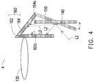
- FIG. 4 illustrates rotation of the first light absorbing device 150 of FIG. 3 .
- the photo sensor 140 may be fixed on the first light absorbing device 150.
- the first light absorbing device 150 may drive the photo sensor 140 to rotate, so as to adjust an included angle ⁇ (indicated in FIG. 3 ) between the second part of light L2 and a normal direction N of a light receiving surface 140a of the photo sensor 140.
- the control unit 300 may adjust the included angle ⁇ between the second part of light L2 and the normal direction N of the light receiving surface 140a of the photo sensor 140 according to sensitivity of the photo sensor 140. To be specific, the lower the sensitivity of the photo sensor 140 is, the smaller the included angle ⁇ is.
- the included angle ⁇ may be adjusted according to the sensitivity of the photo sensor 140, so as to optimize the function of the photo sensor 140 for monitoring the intensity of the light L.
- the included angle ⁇ may be decreased to ensure that the photo sensor 140 still plays a good monitoring function.
- the projection unit 100 may further include an optical device 170.
- the optical device 170 is disposed on the transmission path of the light L.
- the optical device 170 reflects the light L coming from the light source 110 to the DMD 120.
- the first part of light L1 reflected by the DMD 120 may pass through the optical device 170 to reach the projection lens 130.
- the optical device 170 may be a total internal reflection (TIR) prism, though the invention is not limited thereto.
- the projection unit 100 may further include a light uniforming device 180.
- the light uniforming device 180 is disposed on the transmission path of the light L, and is located between the light source 110 and the optical device 170.
- the light uniforming device 180 is used for uniforming the light L emitted by the light source 110, or even adjusting a light shape of the light L, such that the light shape of the light L is similar to a shape (for example, a rectangle) of a working region of the DMD 120, so as to improve usage efficiency of the light L.
- the working region of the DMD 120 refers to a region where the first micromirrors 122 and the second micromirrors 124 are located.
- the light uniforming device 180 is, for example, a micro-lens array, though the invention is not limited thereto.
- the projection unit 100 may further include a light converging device 190.
- the light converging device 190 is disposed on the transmission path of the light L.
- the light converging device 190 is selectively located between the light uniforming device 180 and the optical device 170. Through the light converging device 190, the light L coming from the light source 110 may be converged to the optical device 170, so as to be transmitted to the DMD 120.
- the light converging device 190 is, for example, a lens set, though the invention is not limited thereto.
- FIG. 5 is an enlarged view of the projection lens 130, the photo sensor 140, the first light absorbing device 150 and a second light absorbing device 160A of the 3D printing device according to another embodiment of the invention.
- a light absorbing surface 166 of the second light absorbing device 160A may be a plane, and the light absorbing surface 166 of the second light absorbing device 160A may be inclined relative to the optical axis A of the projection lens 130.
- the second light absorbing device 160A has a similar function with that of the aforementioned second light absorbing device 160, and detail thereof is not repeated.
- FIG. 6 is an enlarged view of the projection lens 130, the photo sensor 140, the first light absorbing device 150 and a second light absorbing device 160B of the 3D printing device according to still another embodiment of the invention.
- a light absorbing surface 168 of the second light absorbing device 160B may be a curved surface, which is, for example but not limited to, a concave surface.
- the second light absorbing device 160B has a similar function with that of the aforementioned second light absorbing device 160, and detail thereof is not repeated.
- the 3D printing apparatus of the invention includes a light source, a DMD, a projection lens and a photo sensor.
- the light source is used for emitting a light.
- the DMD is disposed on a transmission path of the light, and has a plurality of first micromirrors and a plurality of second micromirrors.
- the first micromirrors reflect a first part of light to the projection lens.
- the projection lens projects the first part of light to a working liquid to cure the working liquid.
- the second micromirrors reflect a second part of light to the outside of the projection lens.
- the photo sensor is disposed on a transmission path of the second part of light.
- an intensity of the second part of light measured by the photo sensor By monitoring an intensity of the second part of light measured by the photo sensor, it is determined whether an intensity of the light emitted by the light source is decayed. If it is determined that the intensity of the light is decayed, the intensity of the light is increased to an ideal value. In this way, during the 3D printing process, the intensity of the first part of light projected to the working liquid may be maintained to an ideal value, so as to print the stable 3D printing object with good quality. More importantly, since the photo sensor is disposed on the transmission path of the second part of light (i.e. the non-image light), allocation of the photo sensor does not influence an image resolution and/or an image range.
Applications Claiming Priority (1)
| Application Number | Priority Date | Filing Date | Title |
|---|---|---|---|
| CN201710957270.5A CN109664502A (zh) | 2017-10-16 | 2017-10-16 | 立体打印装置 |
Publications (2)
| Publication Number | Publication Date |
|---|---|
| EP3470210A1 true EP3470210A1 (fr) | 2019-04-17 |
| EP3470210B1 EP3470210B1 (fr) | 2020-09-09 |
Family
ID=63014338
Family Applications (1)
| Application Number | Title | Priority Date | Filing Date |
|---|---|---|---|
| EP18184595.9A Active EP3470210B1 (fr) | 2017-10-16 | 2018-07-20 | Imprimante tridimensionnelle |
Country Status (5)
| Country | Link |
|---|---|
| US (1) | US20190111624A1 (fr) |
| EP (1) | EP3470210B1 (fr) |
| JP (1) | JP6764905B2 (fr) |
| CN (1) | CN109664502A (fr) |
| ES (1) | ES2829601T3 (fr) |
Cited By (1)
| Publication number | Priority date | Publication date | Assignee | Title |
|---|---|---|---|---|
| EP3702130A1 (fr) * | 2019-02-27 | 2020-09-02 | Ivoclar Vivadent AG | Appareil de stéréolithographie et procédé d'ajustement d'un appareil de stéréolithographie |
Families Citing this family (1)
| Publication number | Priority date | Publication date | Assignee | Title |
|---|---|---|---|---|
| US11241832B2 (en) | 2019-07-08 | 2022-02-08 | Hewlett Packard Development Company, L.P. | Energy emitting apparatuses for build material layers |
Citations (2)
| Publication number | Priority date | Publication date | Assignee | Title |
|---|---|---|---|---|
| US20020051141A1 (en) * | 1999-12-24 | 2002-05-02 | Eiichi Kito | Printer and projector equipped with micromirror device |
| JP2004223774A (ja) * | 2003-01-20 | 2004-08-12 | Murakawa Masao | 薄膜硬化型光造形方法および装置 |
Family Cites Families (10)
| Publication number | Priority date | Publication date | Assignee | Title |
|---|---|---|---|---|
| DE29513026U1 (de) * | 1995-08-16 | 1995-10-05 | Eos Electro Optical Syst | Vorrichtung zur schichtweisen Herstellung eines Objektes mittels Lasersintern |
| WO2002027408A2 (fr) * | 2000-09-27 | 2002-04-04 | The Regents Of The University Of California | Microstereolithographie par projection de masque dynamique |
| US7230964B2 (en) * | 2001-04-09 | 2007-06-12 | Cymer, Inc. | Lithography laser with beam delivery and beam pointing control |
| JP4669843B2 (ja) * | 2004-09-29 | 2011-04-13 | ナブテスコ株式会社 | 光造形装置及び光造形方法 |
| CN100403092C (zh) * | 2005-05-16 | 2008-07-16 | 中强光电股份有限公司 | 光学投影装置 |
| CN100465775C (zh) * | 2005-06-17 | 2009-03-04 | 扬明光学股份有限公司 | 数字光源处理投影装置 |
| CN201607576U (zh) * | 2010-04-06 | 2010-10-13 | 深圳市爱美得科技有限公司 | 一种数字光处理投影装置 |
| US9034237B2 (en) * | 2012-09-25 | 2015-05-19 | 3D Systems, Inc. | Solid imaging systems, components thereof, and methods of solid imaging |
| US10308007B2 (en) * | 2015-06-18 | 2019-06-04 | University Of Southern California | Mask video projection based stereolithography with continuous resin flow |
| CN107031035B (zh) * | 2016-02-02 | 2019-07-12 | 三纬国际立体列印科技股份有限公司 | 立体物件成型系统及其校正方法 |
-
2017
- 2017-10-16 CN CN201710957270.5A patent/CN109664502A/zh active Pending
-
2018
- 2018-04-17 US US15/955,645 patent/US20190111624A1/en not_active Abandoned
- 2018-07-20 EP EP18184595.9A patent/EP3470210B1/fr active Active
- 2018-07-20 ES ES18184595T patent/ES2829601T3/es active Active
- 2018-07-23 JP JP2018137415A patent/JP6764905B2/ja active Active
Patent Citations (2)
| Publication number | Priority date | Publication date | Assignee | Title |
|---|---|---|---|---|
| US20020051141A1 (en) * | 1999-12-24 | 2002-05-02 | Eiichi Kito | Printer and projector equipped with micromirror device |
| JP2004223774A (ja) * | 2003-01-20 | 2004-08-12 | Murakawa Masao | 薄膜硬化型光造形方法および装置 |
Cited By (1)
| Publication number | Priority date | Publication date | Assignee | Title |
|---|---|---|---|---|
| EP3702130A1 (fr) * | 2019-02-27 | 2020-09-02 | Ivoclar Vivadent AG | Appareil de stéréolithographie et procédé d'ajustement d'un appareil de stéréolithographie |
Also Published As
| Publication number | Publication date |
|---|---|
| JP6764905B2 (ja) | 2020-10-07 |
| EP3470210B1 (fr) | 2020-09-09 |
| CN109664502A (zh) | 2019-04-23 |
| US20190111624A1 (en) | 2019-04-18 |
| JP2019072996A (ja) | 2019-05-16 |
| ES2829601T3 (es) | 2021-06-01 |
Similar Documents
| Publication | Publication Date | Title |
|---|---|---|
| EP3162542B1 (fr) | Procédé pour étalonner une lumière d'un appareil de génération d'objet tridimensionnel | |
| TWI548533B (zh) | 立體列印裝置 | |
| US9632420B2 (en) | Production of a volume object by lithography, having improved spatial resolution | |
| WO2015081756A1 (fr) | Dispositif d'impression 3d à photodurcissement et son système d'imagerie | |
| WO2015180022A1 (fr) | Système d'impression 3d | |
| US10751942B2 (en) | Three-dimensional printing device | |
| JP7165761B2 (ja) | 統合走査モジュール較正を備えた三次元プリントシステム | |
| US10933578B2 (en) | Pattern forming sheet, pattern manufacturing apparatus, and pattern manufacturing method | |
| EP3470210B1 (fr) | Imprimante tridimensionnelle | |
| KR101798533B1 (ko) | 3차원 프린터에 의한 조형 장치 및 방법 | |
| JP6668004B2 (ja) | 回路パターン製造装置、回路パターン製造方法および回路パターン製造プログラム | |
| US20170028647A1 (en) | Three dimensional printing system | |
| WO2020095453A1 (fr) | Dispositif de stratification/moulage | |
| CN212684740U (zh) | 能量辐射系统及3d打印设备 | |
| CN113119459B (zh) | 3d打印设备的标定系统、方法及3d打印设备 | |
| JP6833431B2 (ja) | 光造形装置、光造形方法および光造形プログラム | |
| CN114228153B (zh) | 双激光头标定方法 | |
| JP7084507B2 (ja) | 外部振動に応答する三次元プリンタ | |
| CN114261088B (zh) | 能量辐射装置的幅面亮度检测方法、系统及标定方法 | |
| JP7084508B2 (ja) | レーザ較正システムを備えた三次元プリントシステム | |
| JP2018179536A (ja) | 液滴測定方法と液滴測定装置 | |
| US20230067468A1 (en) | 3d printing system and method | |
| WO2022176313A1 (fr) | Dispositif de mise en forme optique et procédé de fabrication | |
| JP7183763B2 (ja) | 三次元物体の造形装置および造形方法 | |
| US20220405960A1 (en) | Contactless location information acquisition apparatus and location information acquisition method using the same |
Legal Events
| Date | Code | Title | Description |
|---|---|---|---|
| PUAI | Public reference made under article 153(3) epc to a published international application that has entered the european phase |
Free format text: ORIGINAL CODE: 0009012 |
|
| STAA | Information on the status of an ep patent application or granted ep patent |
Free format text: STATUS: THE APPLICATION HAS BEEN PUBLISHED |
|
| AK | Designated contracting states |
Kind code of ref document: A1 Designated state(s): AL AT BE BG CH CY CZ DE DK EE ES FI FR GB GR HR HU IE IS IT LI LT LU LV MC MK MT NL NO PL PT RO RS SE SI SK SM TR |
|
| AX | Request for extension of the european patent |
Extension state: BA ME |
|
| STAA | Information on the status of an ep patent application or granted ep patent |
Free format text: STATUS: REQUEST FOR EXAMINATION WAS MADE |
|
| 17P | Request for examination filed |
Effective date: 20191016 |
|
| RBV | Designated contracting states (corrected) |
Designated state(s): AL AT BE BG CH CY CZ DE DK EE ES FI FR GB GR HR HU IE IS IT LI LT LU LV MC MK MT NL NO PL PT RO RS SE SI SK SM TR |
|
| RIC1 | Information provided on ipc code assigned before grant |
Ipc: B29C 64/124 20170101ALI20200320BHEP Ipc: B29C 64/277 20170101AFI20200320BHEP Ipc: B33Y 30/00 20150101ALI20200320BHEP |
|
| GRAP | Despatch of communication of intention to grant a patent |
Free format text: ORIGINAL CODE: EPIDOSNIGR1 |
|
| STAA | Information on the status of an ep patent application or granted ep patent |
Free format text: STATUS: GRANT OF PATENT IS INTENDED |
|
| INTG | Intention to grant announced |
Effective date: 20200508 |
|
| GRAS | Grant fee paid |
Free format text: ORIGINAL CODE: EPIDOSNIGR3 |
|
| GRAA | (expected) grant |
Free format text: ORIGINAL CODE: 0009210 |
|
| STAA | Information on the status of an ep patent application or granted ep patent |
Free format text: STATUS: THE PATENT HAS BEEN GRANTED |
|
| AK | Designated contracting states |
Kind code of ref document: B1 Designated state(s): AL AT BE BG CH CY CZ DE DK EE ES FI FR GB GR HR HU IE IS IT LI LT LU LV MC MK MT NL NO PL PT RO RS SE SI SK SM TR |
|
| REG | Reference to a national code |
Ref country code: GB Ref legal event code: FG4D |
|
| REG | Reference to a national code |
Ref country code: AT Ref legal event code: REF Ref document number: 1311039 Country of ref document: AT Kind code of ref document: T Effective date: 20200915 Ref country code: CH Ref legal event code: EP |
|
| REG | Reference to a national code |
Ref country code: IE Ref legal event code: FG4D |
|
| REG | Reference to a national code |
Ref country code: DE Ref legal event code: R096 Ref document number: 602018007559 Country of ref document: DE |
|
| REG | Reference to a national code |
Ref country code: LT Ref legal event code: MG4D |
|
| PG25 | Lapsed in a contracting state [announced via postgrant information from national office to epo] |
Ref country code: FI Free format text: LAPSE BECAUSE OF FAILURE TO SUBMIT A TRANSLATION OF THE DESCRIPTION OR TO PAY THE FEE WITHIN THE PRESCRIBED TIME-LIMIT Effective date: 20200909 Ref country code: SE Free format text: LAPSE BECAUSE OF FAILURE TO SUBMIT A TRANSLATION OF THE DESCRIPTION OR TO PAY THE FEE WITHIN THE PRESCRIBED TIME-LIMIT Effective date: 20200909 Ref country code: BG Free format text: LAPSE BECAUSE OF FAILURE TO SUBMIT A TRANSLATION OF THE DESCRIPTION OR TO PAY THE FEE WITHIN THE PRESCRIBED TIME-LIMIT Effective date: 20201209 Ref country code: HR Free format text: LAPSE BECAUSE OF FAILURE TO SUBMIT A TRANSLATION OF THE DESCRIPTION OR TO PAY THE FEE WITHIN THE PRESCRIBED TIME-LIMIT Effective date: 20200909 Ref country code: NO Free format text: LAPSE BECAUSE OF FAILURE TO SUBMIT A TRANSLATION OF THE DESCRIPTION OR TO PAY THE FEE WITHIN THE PRESCRIBED TIME-LIMIT Effective date: 20201209 Ref country code: GR Free format text: LAPSE BECAUSE OF FAILURE TO SUBMIT A TRANSLATION OF THE DESCRIPTION OR TO PAY THE FEE WITHIN THE PRESCRIBED TIME-LIMIT Effective date: 20201210 Ref country code: LT Free format text: LAPSE BECAUSE OF FAILURE TO SUBMIT A TRANSLATION OF THE DESCRIPTION OR TO PAY THE FEE WITHIN THE PRESCRIBED TIME-LIMIT Effective date: 20200909 |
|
| REG | Reference to a national code |
Ref country code: AT Ref legal event code: MK05 Ref document number: 1311039 Country of ref document: AT Kind code of ref document: T Effective date: 20200909 |
|
| REG | Reference to a national code |
Ref country code: NL Ref legal event code: MP Effective date: 20200909 |
|
| PG25 | Lapsed in a contracting state [announced via postgrant information from national office to epo] |
Ref country code: PL Free format text: LAPSE BECAUSE OF FAILURE TO SUBMIT A TRANSLATION OF THE DESCRIPTION OR TO PAY THE FEE WITHIN THE PRESCRIBED TIME-LIMIT Effective date: 20200909 Ref country code: LV Free format text: LAPSE BECAUSE OF FAILURE TO SUBMIT A TRANSLATION OF THE DESCRIPTION OR TO PAY THE FEE WITHIN THE PRESCRIBED TIME-LIMIT Effective date: 20200909 Ref country code: RS Free format text: LAPSE BECAUSE OF FAILURE TO SUBMIT A TRANSLATION OF THE DESCRIPTION OR TO PAY THE FEE WITHIN THE PRESCRIBED TIME-LIMIT Effective date: 20200909 |
|
| PG25 | Lapsed in a contracting state [announced via postgrant information from national office to epo] |
Ref country code: CZ Free format text: LAPSE BECAUSE OF FAILURE TO SUBMIT A TRANSLATION OF THE DESCRIPTION OR TO PAY THE FEE WITHIN THE PRESCRIBED TIME-LIMIT Effective date: 20200909 Ref country code: PT Free format text: LAPSE BECAUSE OF FAILURE TO SUBMIT A TRANSLATION OF THE DESCRIPTION OR TO PAY THE FEE WITHIN THE PRESCRIBED TIME-LIMIT Effective date: 20210111 Ref country code: RO Free format text: LAPSE BECAUSE OF FAILURE TO SUBMIT A TRANSLATION OF THE DESCRIPTION OR TO PAY THE FEE WITHIN THE PRESCRIBED TIME-LIMIT Effective date: 20200909 Ref country code: EE Free format text: LAPSE BECAUSE OF FAILURE TO SUBMIT A TRANSLATION OF THE DESCRIPTION OR TO PAY THE FEE WITHIN THE PRESCRIBED TIME-LIMIT Effective date: 20200909 Ref country code: SM Free format text: LAPSE BECAUSE OF FAILURE TO SUBMIT A TRANSLATION OF THE DESCRIPTION OR TO PAY THE FEE WITHIN THE PRESCRIBED TIME-LIMIT Effective date: 20200909 |
|
| PG25 | Lapsed in a contracting state [announced via postgrant information from national office to epo] |
Ref country code: IS Free format text: LAPSE BECAUSE OF FAILURE TO SUBMIT A TRANSLATION OF THE DESCRIPTION OR TO PAY THE FEE WITHIN THE PRESCRIBED TIME-LIMIT Effective date: 20210109 Ref country code: AL Free format text: LAPSE BECAUSE OF FAILURE TO SUBMIT A TRANSLATION OF THE DESCRIPTION OR TO PAY THE FEE WITHIN THE PRESCRIBED TIME-LIMIT Effective date: 20200909 Ref country code: AT Free format text: LAPSE BECAUSE OF FAILURE TO SUBMIT A TRANSLATION OF THE DESCRIPTION OR TO PAY THE FEE WITHIN THE PRESCRIBED TIME-LIMIT Effective date: 20200909 |
|
| REG | Reference to a national code |
Ref country code: ES Ref legal event code: FG2A Ref document number: 2829601 Country of ref document: ES Kind code of ref document: T3 Effective date: 20210601 |
|
| REG | Reference to a national code |
Ref country code: DE Ref legal event code: R097 Ref document number: 602018007559 Country of ref document: DE |
|
| PG25 | Lapsed in a contracting state [announced via postgrant information from national office to epo] |
Ref country code: SK Free format text: LAPSE BECAUSE OF FAILURE TO SUBMIT A TRANSLATION OF THE DESCRIPTION OR TO PAY THE FEE WITHIN THE PRESCRIBED TIME-LIMIT Effective date: 20200909 |
|
| PLBE | No opposition filed within time limit |
Free format text: ORIGINAL CODE: 0009261 |
|
| STAA | Information on the status of an ep patent application or granted ep patent |
Free format text: STATUS: NO OPPOSITION FILED WITHIN TIME LIMIT |
|
| 26N | No opposition filed |
Effective date: 20210610 |
|
| PG25 | Lapsed in a contracting state [announced via postgrant information from national office to epo] |
Ref country code: SI Free format text: LAPSE BECAUSE OF FAILURE TO SUBMIT A TRANSLATION OF THE DESCRIPTION OR TO PAY THE FEE WITHIN THE PRESCRIBED TIME-LIMIT Effective date: 20200909 Ref country code: DK Free format text: LAPSE BECAUSE OF FAILURE TO SUBMIT A TRANSLATION OF THE DESCRIPTION OR TO PAY THE FEE WITHIN THE PRESCRIBED TIME-LIMIT Effective date: 20200909 |
|
| PGFP | Annual fee paid to national office [announced via postgrant information from national office to epo] |
Ref country code: IT Payment date: 20210731 Year of fee payment: 4 |
|
| REG | Reference to a national code |
Ref country code: DE Ref legal event code: R119 Ref document number: 602018007559 Country of ref document: DE |
|
| REG | Reference to a national code |
Ref country code: CH Ref legal event code: PL |
|
| PG25 | Lapsed in a contracting state [announced via postgrant information from national office to epo] |
Ref country code: MC Free format text: LAPSE BECAUSE OF FAILURE TO SUBMIT A TRANSLATION OF THE DESCRIPTION OR TO PAY THE FEE WITHIN THE PRESCRIBED TIME-LIMIT Effective date: 20200909 |
|
| REG | Reference to a national code |
Ref country code: BE Ref legal event code: MM Effective date: 20210731 |
|
| PG25 | Lapsed in a contracting state [announced via postgrant information from national office to epo] |
Ref country code: LI Free format text: LAPSE BECAUSE OF NON-PAYMENT OF DUE FEES Effective date: 20210731 Ref country code: DE Free format text: LAPSE BECAUSE OF NON-PAYMENT OF DUE FEES Effective date: 20220201 Ref country code: CH Free format text: LAPSE BECAUSE OF NON-PAYMENT OF DUE FEES Effective date: 20210731 |
|
| PG25 | Lapsed in a contracting state [announced via postgrant information from national office to epo] |
Ref country code: LU Free format text: LAPSE BECAUSE OF NON-PAYMENT OF DUE FEES Effective date: 20210720 Ref country code: FR Free format text: LAPSE BECAUSE OF NON-PAYMENT OF DUE FEES Effective date: 20210731 |
|
| PG25 | Lapsed in a contracting state [announced via postgrant information from national office to epo] |
Ref country code: IE Free format text: LAPSE BECAUSE OF NON-PAYMENT OF DUE FEES Effective date: 20210720 Ref country code: BE Free format text: LAPSE BECAUSE OF NON-PAYMENT OF DUE FEES Effective date: 20210731 |
|
| REG | Reference to a national code |
Ref country code: ES Ref legal event code: FD2A Effective date: 20220826 |
|
| PG25 | Lapsed in a contracting state [announced via postgrant information from national office to epo] |
Ref country code: ES Free format text: LAPSE BECAUSE OF NON-PAYMENT OF DUE FEES Effective date: 20210721 |
|
| GBPC | Gb: european patent ceased through non-payment of renewal fee |
Effective date: 20220720 |
|
| PG25 | Lapsed in a contracting state [announced via postgrant information from national office to epo] |
Ref country code: GB Free format text: LAPSE BECAUSE OF NON-PAYMENT OF DUE FEES Effective date: 20220720 |
|
| PG25 | Lapsed in a contracting state [announced via postgrant information from national office to epo] |
Ref country code: NL Free format text: LAPSE BECAUSE OF NON-PAYMENT OF DUE FEES Effective date: 20200923 Ref country code: CY Free format text: LAPSE BECAUSE OF FAILURE TO SUBMIT A TRANSLATION OF THE DESCRIPTION OR TO PAY THE FEE WITHIN THE PRESCRIBED TIME-LIMIT Effective date: 20200909 |
|
| PG25 | Lapsed in a contracting state [announced via postgrant information from national office to epo] |
Ref country code: IT Free format text: LAPSE BECAUSE OF NON-PAYMENT OF DUE FEES Effective date: 20220720 Ref country code: HU Free format text: LAPSE BECAUSE OF FAILURE TO SUBMIT A TRANSLATION OF THE DESCRIPTION OR TO PAY THE FEE WITHIN THE PRESCRIBED TIME-LIMIT; INVALID AB INITIO Effective date: 20180720 |
|
| PG25 | Lapsed in a contracting state [announced via postgrant information from national office to epo] |
Ref country code: MK Free format text: LAPSE BECAUSE OF FAILURE TO SUBMIT A TRANSLATION OF THE DESCRIPTION OR TO PAY THE FEE WITHIN THE PRESCRIBED TIME-LIMIT Effective date: 20200909 |