EP3469314B1 - Magnetfeldsensor zur erfassung einer nähe und/oder eines standorts eines objekts - Google Patents
Magnetfeldsensor zur erfassung einer nähe und/oder eines standorts eines objekts Download PDFInfo
- Publication number
- EP3469314B1 EP3469314B1 EP17726478.5A EP17726478A EP3469314B1 EP 3469314 B1 EP3469314 B1 EP 3469314B1 EP 17726478 A EP17726478 A EP 17726478A EP 3469314 B1 EP3469314 B1 EP 3469314B1
- Authority
- EP
- European Patent Office
- Prior art keywords
- magnetic field
- substrate
- field sensing
- sensing element
- field sensor
- Prior art date
- Legal status (The legal status is an assumption and is not a legal conclusion. Google has not performed a legal analysis and makes no representation as to the accuracy of the status listed.)
- Active
Links
- 230000005291 magnetic effect Effects 0.000 title claims description 297
- 239000000758 substrate Substances 0.000 claims description 190
- 230000005355 Hall effect Effects 0.000 claims description 114
- 230000005294 ferromagnetic effect Effects 0.000 claims description 114
- 239000004065 semiconductor Substances 0.000 claims description 32
- 230000035945 sensitivity Effects 0.000 claims description 22
- 230000008859 change Effects 0.000 claims description 13
- 230000033001 locomotion Effects 0.000 claims description 10
- 230000000295 complement effect Effects 0.000 claims 4
- 230000004044 response Effects 0.000 description 20
- 238000013459 approach Methods 0.000 description 11
- 238000010586 diagram Methods 0.000 description 11
- 230000008878 coupling Effects 0.000 description 8
- 238000010168 coupling process Methods 0.000 description 8
- 238000005859 coupling reaction Methods 0.000 description 8
- 230000006870 function Effects 0.000 description 8
- 238000009987 spinning Methods 0.000 description 6
- CWYNVVGOOAEACU-UHFFFAOYSA-N Fe2+ Chemical compound [Fe+2] CWYNVVGOOAEACU-UHFFFAOYSA-N 0.000 description 4
- 230000004807 localization Effects 0.000 description 4
- 238000004519 manufacturing process Methods 0.000 description 4
- 238000000034 method Methods 0.000 description 4
- 238000000926 separation method Methods 0.000 description 4
- 230000004907 flux Effects 0.000 description 2
- WPYVAWXEWQSOGY-UHFFFAOYSA-N indium antimonide Chemical compound [Sb]#[In] WPYVAWXEWQSOGY-UHFFFAOYSA-N 0.000 description 2
- 239000000463 material Substances 0.000 description 2
- 229910052751 metal Inorganic materials 0.000 description 2
- 239000002184 metal Substances 0.000 description 2
- JBRZTFJDHDCESZ-UHFFFAOYSA-N AsGa Chemical compound [As]#[Ga] JBRZTFJDHDCESZ-UHFFFAOYSA-N 0.000 description 1
- XUIMIQQOPSSXEZ-UHFFFAOYSA-N Silicon Chemical compound [Si] XUIMIQQOPSSXEZ-UHFFFAOYSA-N 0.000 description 1
- 230000004888 barrier function Effects 0.000 description 1
- 230000015572 biosynthetic process Effects 0.000 description 1
- 239000003990 capacitor Substances 0.000 description 1
- 238000006243 chemical reaction Methods 0.000 description 1
- 150000001875 compounds Chemical class 0.000 description 1
- 239000004020 conductor Substances 0.000 description 1
- 238000009792 diffusion process Methods 0.000 description 1
- -1 e.g. Chemical compound 0.000 description 1
- 230000000694 effects Effects 0.000 description 1
- 230000005684 electric field Effects 0.000 description 1
- 229910052732 germanium Inorganic materials 0.000 description 1
- GNPVGFCGXDBREM-UHFFFAOYSA-N germanium atom Chemical compound [Ge] GNPVGFCGXDBREM-UHFFFAOYSA-N 0.000 description 1
- 239000007943 implant Substances 0.000 description 1
- 150000002472 indium compounds Chemical class 0.000 description 1
- 230000001939 inductive effect Effects 0.000 description 1
- 230000005381 magnetic domain Effects 0.000 description 1
- 230000000306 recurrent effect Effects 0.000 description 1
- 229910052710 silicon Inorganic materials 0.000 description 1
- 239000010703 silicon Substances 0.000 description 1
- 230000005641 tunneling Effects 0.000 description 1
Images


Classifications
-
- G—PHYSICS
- G01—MEASURING; TESTING
- G01D—MEASURING NOT SPECIALLY ADAPTED FOR A SPECIFIC VARIABLE; ARRANGEMENTS FOR MEASURING TWO OR MORE VARIABLES NOT COVERED IN A SINGLE OTHER SUBCLASS; TARIFF METERING APPARATUS; MEASURING OR TESTING NOT OTHERWISE PROVIDED FOR
- G01D5/00—Mechanical means for transferring the output of a sensing member; Means for converting the output of a sensing member to another variable where the form or nature of the sensing member does not constrain the means for converting; Transducers not specially adapted for a specific variable
- G01D5/12—Mechanical means for transferring the output of a sensing member; Means for converting the output of a sensing member to another variable where the form or nature of the sensing member does not constrain the means for converting; Transducers not specially adapted for a specific variable using electric or magnetic means
- G01D5/14—Mechanical means for transferring the output of a sensing member; Means for converting the output of a sensing member to another variable where the form or nature of the sensing member does not constrain the means for converting; Transducers not specially adapted for a specific variable using electric or magnetic means influencing the magnitude of a current or voltage
- G01D5/142—Mechanical means for transferring the output of a sensing member; Means for converting the output of a sensing member to another variable where the form or nature of the sensing member does not constrain the means for converting; Transducers not specially adapted for a specific variable using electric or magnetic means influencing the magnitude of a current or voltage using Hall-effect devices
-
- G—PHYSICS
- G01—MEASURING; TESTING
- G01P—MEASURING LINEAR OR ANGULAR SPEED, ACCELERATION, DECELERATION, OR SHOCK; INDICATING PRESENCE, ABSENCE, OR DIRECTION, OF MOVEMENT
- G01P3/00—Measuring linear or angular speed; Measuring differences of linear or angular speeds
- G01P3/42—Devices characterised by the use of electric or magnetic means
- G01P3/44—Devices characterised by the use of electric or magnetic means for measuring angular speed
- G01P3/48—Devices characterised by the use of electric or magnetic means for measuring angular speed by measuring frequency of generated current or voltage
- G01P3/481—Devices characterised by the use of electric or magnetic means for measuring angular speed by measuring frequency of generated current or voltage of pulse signals
- G01P3/488—Devices characterised by the use of electric or magnetic means for measuring angular speed by measuring frequency of generated current or voltage of pulse signals delivered by variable reluctance detectors
-
- G—PHYSICS
- G01—MEASURING; TESTING
- G01B—MEASURING LENGTH, THICKNESS OR SIMILAR LINEAR DIMENSIONS; MEASURING ANGLES; MEASURING AREAS; MEASURING IRREGULARITIES OF SURFACES OR CONTOURS
- G01B7/00—Measuring arrangements characterised by the use of electric or magnetic techniques
- G01B7/02—Measuring arrangements characterised by the use of electric or magnetic techniques for measuring length, width or thickness
- G01B7/023—Measuring arrangements characterised by the use of electric or magnetic techniques for measuring length, width or thickness for measuring distance between sensor and object
-
- G—PHYSICS
- G01—MEASURING; TESTING
- G01D—MEASURING NOT SPECIALLY ADAPTED FOR A SPECIFIC VARIABLE; ARRANGEMENTS FOR MEASURING TWO OR MORE VARIABLES NOT COVERED IN A SINGLE OTHER SUBCLASS; TARIFF METERING APPARATUS; MEASURING OR TESTING NOT OTHERWISE PROVIDED FOR
- G01D5/00—Mechanical means for transferring the output of a sensing member; Means for converting the output of a sensing member to another variable where the form or nature of the sensing member does not constrain the means for converting; Transducers not specially adapted for a specific variable
- G01D5/12—Mechanical means for transferring the output of a sensing member; Means for converting the output of a sensing member to another variable where the form or nature of the sensing member does not constrain the means for converting; Transducers not specially adapted for a specific variable using electric or magnetic means
- G01D5/14—Mechanical means for transferring the output of a sensing member; Means for converting the output of a sensing member to another variable where the form or nature of the sensing member does not constrain the means for converting; Transducers not specially adapted for a specific variable using electric or magnetic means influencing the magnitude of a current or voltage
- G01D5/142—Mechanical means for transferring the output of a sensing member; Means for converting the output of a sensing member to another variable where the form or nature of the sensing member does not constrain the means for converting; Transducers not specially adapted for a specific variable using electric or magnetic means influencing the magnitude of a current or voltage using Hall-effect devices
- G01D5/147—Mechanical means for transferring the output of a sensing member; Means for converting the output of a sensing member to another variable where the form or nature of the sensing member does not constrain the means for converting; Transducers not specially adapted for a specific variable using electric or magnetic means influencing the magnitude of a current or voltage using Hall-effect devices influenced by the movement of a third element, the position of Hall device and the source of magnetic field being fixed in respect to each other
-
- G—PHYSICS
- G01—MEASURING; TESTING
- G01D—MEASURING NOT SPECIALLY ADAPTED FOR A SPECIFIC VARIABLE; ARRANGEMENTS FOR MEASURING TWO OR MORE VARIABLES NOT COVERED IN A SINGLE OTHER SUBCLASS; TARIFF METERING APPARATUS; MEASURING OR TESTING NOT OTHERWISE PROVIDED FOR
- G01D5/00—Mechanical means for transferring the output of a sensing member; Means for converting the output of a sensing member to another variable where the form or nature of the sensing member does not constrain the means for converting; Transducers not specially adapted for a specific variable
- G01D5/12—Mechanical means for transferring the output of a sensing member; Means for converting the output of a sensing member to another variable where the form or nature of the sensing member does not constrain the means for converting; Transducers not specially adapted for a specific variable using electric or magnetic means
- G01D5/14—Mechanical means for transferring the output of a sensing member; Means for converting the output of a sensing member to another variable where the form or nature of the sensing member does not constrain the means for converting; Transducers not specially adapted for a specific variable using electric or magnetic means influencing the magnitude of a current or voltage
- G01D5/16—Mechanical means for transferring the output of a sensing member; Means for converting the output of a sensing member to another variable where the form or nature of the sensing member does not constrain the means for converting; Transducers not specially adapted for a specific variable using electric or magnetic means influencing the magnitude of a current or voltage by varying resistance
Definitions
- This invention relates generally to magnetic field sensors and, more particularly, to a back-biased magnetic field sensor that can sense both a proximity and/or a location of a ferromagnetic object.
- Magnetic field sensors generally include a magnetic field sensing element and other electronic components. Some magnetic field sensors also include a permanent magnet in a so-called "back biased" arrangement described more fully below.
- Magnetic field sensors provide an electrical signal representative of a sensed magnetic field, e.g., a magnitude of the sensed magnetic field.
- a magnetic field sensed by a magnetic field sensor is a magnetic field generated primarily by the magnet.
- the magnetic field generated by the magnet and sensed by the magnetic field sensor varies in accordance with proximity of the ferromagnetic object to the magnetic field sensor.
- the output signal from the magnetic field sensor is a "nonlinear" two state signal having a first state indicative of a ferromagnetic object being distal from the magnetic field sensor and a second different state indicative of the ferromagnetic object being proximate to the magnetic field sensor.
- the output signal from the magnetic field sensor is a "linear” (analog or digital) signal having a signal value indicative of a distance between the ferromagnetic object and the magnetic field sensor.
- a magnetic field sensor having either of the above signal characteristics can be referred to as a "proximity sensor.”
- Conventional back-biased proximity sensors are able to sense a proximity of a ferromagnetic object (i.e., distance between the back biased proximity sensor and the ferromagnetic object) but are not able to identify a location of the ferromagnetic object, for example, a location in an x-y plane of the back-biased proximity sensor, for example, where the ferromagnetic object approaches the magnetic field sensor in a z direction.
- a back-biased proximity sensor that it able to sense not only a proximity of a ferromagnetic object (i.e., distance between the back biased proximity sensor and the ferromagnetic object) but is also able to identify a location of the ferromagnetic object, for example, a location in an x-y plane of the back-biased proximity sensor, for example, where the ferromagnetic object approaches the magnetic field sensor in a z direction.
- Conventional back-biased proximity sensors typically use a single ended configuration with one magnetic field sensing element, typically a planar Hall effect element, with a maximum response axis that intersects the ferromagnetic object.
- one magnetic field sensing element typically a planar Hall effect element
- two or more magnetic field sensing elements are used and a difference signal is generated from the two or magnetic field sensing elements.
- the difference signal is representative of an edge of a feature (e.g., gear tooth) of the ferromagnetic object.
- differential arrangements can offer advantages not found in conventional back-biased proximity sensors.
- a differential arrangement that uses two magnetic field sensing elements can be non-responsive to undesirable external magnetic fields that are equally received by the two magnetic field sensing elements.
- the differential arrangement provides common mode rejection.
- a differential arrangement using two planar Hall effect elements would not function properly as a proximity sensor, because both of the two planar Hall effect elements would respond in the same way to a proximate ferromagnetic object and a resulting differential combination would have no output.
- US 2003/222642 A1 relates to an arrangement for determining the position of a motion sensor element influencing the formation of a magnetic field of a working magnet periodically along its motion co-ordinate.
- the arrangement comprises a sensor arrangement, which is sensitive along a measuring direction.
- the motion sensor element arranged in a strip-shaped zone of a main surface extending along the motion co-ordinate of the motion sensor element, comprises periodically recurrent areas alternately influencing the measuring field.
- the sensor arrangement is formed as a magnetoresistive sensor arrangement with at least one half bridge comprising at least two magnetoresistive sensor elements, which sensor elements are sensitive along the measuring direction.
- US 4 481 469 A provides a speed sensor system that requires only one inductive pick-up, and little network circuitry.
- a toothed rotary element is exposed to a magnetic field responsive sensor, such as a Hall generator.
- Means are provided to generate an electrical field which includes both the rotary element and the sensor. These means may, for example, be a permanent magnet.
- the sensor is positioned relative to the field to respond to the tangential component of the magnetic field, rather than to the radial component.
- the tangential component of the magnetic field varies symmetrically with respect to a fixed center or null line, and changes only in magnitude; radial components of the air gap, however, change not only the amplitude but also the relative center position of the undulations due to the teeth of the toothed element.
- US 2005/280411 A1 provides a proximity sensor that is capable of producing a relatively large output signal, and in some cases, an output signal that is relatively independent of the speed at which a target passes the sensor.
- the proximity sensor includes a first and second magnetoresistive resistor connected in a bridge configuration. The first magnetoresistive resistor is spaced from the second magnetoresistive resistor along the path of a moving ferrous target.
- a bias magnet source is positioned behind the proximity sensor, and the ferrous target passes in front of the proximity sensor. The ferrous target alters the direction of the bias magnetic field in the vicinity of the first and second magnetoresistive resistors as the ferrous target passes by the proximity sensor.
- Flux concentrators are positioned proximate to each of the first and second magnetoresistive resistors in order help redirect or shunt the magnetic field component produced by the bias magnet source.
- US 4 053 829 A provides apparatus for detecting the direction of a magnetic field.
- the apparatus includes a magnetoresistive device comprising an insulating substrate, first and second ferromagnetic metal film strips on the substrate for providing first and second main current conducting paths respectively perpendicular to each other, the ends of the strips being connected together to form an output terminal and having current input terminals connected to the opposed ends of the strips.
- a stationary bias magnet is disposed adjacent the magnetoresistive device for supplying a bias flux at a predetermined angle relative to a main current conducting path.
- US 2016/123771 A1 provides a magnetic field sensor that is able to achieve an output signal that accurately differentiates between gear teeth and gear valleys, even in the presence of variations of mechanical and thermal parameters associated with the magnetic field sensor.
- the magnetic field sensor includes a plurality of magnetic field sensing elements disposed upon a major planar surface of a substrate. Each one of the plurality of magnetic field sensing elements has a major response axis substantially parallel to the major planar surface of the substrate.
- the plurality of magnetic field sensing elements is configured to generate a respective plurality of magnetic field signals.
- the present invention provides a back-biased proximity sensor that it able to sense not only a proximity of a ferromagnetic object (i.e., distance between the back biased proximity sensor and the ferromagnetic object) but is also able to identify a location of the ferromagnetic object, for example, a location in an x-y plane of the back-biased proximity sensor, for example, where the ferromagnetic object approaches the magnetic field sensor in a z direction, and is defined by the features of independent claim 1.
- the present invention can provide a back-biased proximity sensor that uses a different type of magnetic field sensing element, different than a planar Hall effect element, and with a maximum response axis that does not intersect the ferromagnetic object
- a magnetic field sensor for sensing a movement of a ferromagnetic object along a path, a movement line tangent to the path, the magnetic field sensor comprises:
- the above magnetic field sensor can include one or more of the following aspects in any combination.
- the above magnetic field sensor further comprises: an electronic circuit coupled to the first magnetic field sensing element and configured to generate a signal having a change of value when the ferromagnetic object moves closer to the semiconductor substrate than a predetermined distance.
- the above magnetic field sensor further comprises: an electronic circuit coupled to the first magnetic field sensing element and configured to generate a signal having a value indicative of a proximity of the ferromagnetic object and proximate to which one of the four half planes the ferromagnetic object is more proximate.
- the first magnetic field sensing element comprises a vertical Hall effect element.
- the first magnetic field sensing element comprises a magnetoresistance element.
- the above magnetic field sensor further comprises: a second magnetic field sensing element disposed on or under the first surface of the semiconductor substrate and disposed within the substrate region, wherein the second magnetic field sensing element comprises an axis of maximum sensitivity substantially parallel to the axis of maximum sensitivity of the first magnetic field sensing element.
- the center of the first magnetic field sensing element is disposed along the second substrate axis, wherein the center of the second magnetic field sensing element is disposed along the second substrate axis and not on the substrate axes point.
- the centers of the first and second magnetic field sensing elements are substantially equidistant from and on opposite sides of the substrate axes point.
- the above magnetic field sensor further comprises: an electronic circuit coupled to the first and second magnetic field sensing elements and configured to generate a signal having a change of value when the ferromagnetic object moves closer to the semiconductor substrate than a predetermined distance.
- the above magnetic field sensor further comprises: an electronic circuit coupled to the first and second magnetic field sensing elements and configured to generate a signal having a value indicative of a proximity of the ferromagnetic object and proximate to which one of the two half planes the ferromagnetic object is more proximate.
- the first and second magnetic field sensing elements comprise vertical Hall effect elements.
- the first and second magnetic field sensing elements comprise magnetoresistance elements.
- the above magnetic field sensor further comprises:
- the center of the first magnetic field sensing element is disposed along the second substrate axis, wherein the center of the second magnetic field sensing element is disposed along the second substrate axis, wherein a center of the third magnetic field sensing element is disposed along the first substrate axis and not on the substrate axes point, wherein a center of the fourth magnetic field sensing element is disposed along the first substrate axis and not on the substrate axes point,
- the centers of the first and second magnetic field sensing elements are substantially equidistant from and on opposite sides of the substrate axes point, and wherein the centers of the third and fourth magnetic field sensing elements are substantially equidistant from and on opposite sides of the substrate axes point.
- the first, second, third, and fourth magnetic field sensing elements are vertical Hall elements within a circular vertical Hall (CVH) sensing element.
- the above magnetic field sensor further comprises: an electronic circuit coupled to the first, second, third, and fourth magnetic field sensing elements and configured to generate a signal having a selected change of value when the ferromagnetic object moves closer to the semiconductor substrate than a predetermined distance.
- the above magnetic field sensor further comprises: an electronic circuit coupled to the first, second, third, and fourth magnetic field sensing elements and configured to generate a signal having a value indicative of a proximity of the ferromagnetic object and proximate to which one of the four planar portions the ferromagnetic object is most proximate.
- the first, second, third, and fourth magnetic field sensing elements comprise vertical Hall effect elements.
- the first, second, third, and fourth magnetic field sensing elements comprise magnetoresistance elements.
- the above magnetic field sensor further comprises: a second magnetic field sensing element disposed on or under the first surface of the semiconductor substrate and disposed within the substrate region, wherein the second magnetic field sensing element comprises an axis of maximum sensitivity substantially perpendicular to the axis of maximum sensitivity of the first magnetic field sensing element.
- a center of the second magnetic field sensing element is disposed along the first substrate axis, and wherein the centers of the first and second magnetic field sensing elements are substantially equidistant from the substrate axes point.
- the above magnetic field sensor further comprises: an electronic circuit coupled to the first and second magnetic field sensing elements and configured to generate a two-state signal having a selected change of state when the ferromagnetic object moves closer to the semiconductor substrate than a predetermined distance.
- the above magnetic field sensor further comprises: an electronic circuit coupled to the first and second magnetic field sensing elements and configured to generate a signal having a value indicative of a proximity of the ferromagnetic object and proximate to which one of the four planar portions the ferromagnetic object is most proximate.
- the first and second magnetic field sensing elements comprise vertical Hall effect elements.
- the first and second magnetic field sensing elements comprise magnetoresistance elements.
- magnetic field sensing element is used to describe a variety of electronic elements that can sense a magnetic field.
- the magnetic field sensing element can be, but is not limited to, a Hall Effect element, a magnetoresistance element, or a magnetotransistor.
- Hall Effect elements for example, a planar Hall element, a vertical Hall element, and a Circular Vertical Hall (CVH) element.
- magnetoresistance elements for example, a semiconductor magnetoresistance element such as Indium Antimonide (InSb), a giant magnetoresistance (GMR) element., an anisotropic magnetoresistance element (AMR), a tunneling magnetoresistance (TMR) element, and a magnetic tunnel junction (MTJ).
- the magnetic field sensing element may be a single element or, alternatively, may include two or more magnetic field sensing elements arranged in various configurations, e.g., a half bridge or full (Wheatstone) bridge.
- the magnetic field sensing element may be a device made of a type IV semiconductor material such as Silicon (Si) or Germanium (Ge), or a compound semiconductor material like Gallium-Arsenide (GaAs) or an Indium compound, e.g., Indium-Antimonide (InSb), or InGaA.
- a type IV semiconductor material such as Silicon (Si) or Germanium (Ge)
- a compound semiconductor material like Gallium-Arsenide (GaAs) or an Indium compound, e.g., Indium-Antimonide (InSb), or InGaA.
- some of the above-described magnetic field sensing elements tend to have an axis of maximum sensitivity substantially parallel to a substrate that supports the magnetic field sensing element, and others of the above-described magnetic field sensing elements tend to have an axis of maximum sensitivity substantially perpendicular to a substrate that supports the magnetic field sensing element.
- planar Hall elements tend to have axes of sensitivity substantially perpendicular to a substrate
- metal based or metallic magnetoresistance elements e.g., GMR, TMR, AMR
- vertical Hall elements tend to have axes of sensitivity parallel to a substrate.
- magnetic field sensor is used to describe a circuit that uses a magnetic field sensing element, generally in combination with other circuits.
- Magnetic field sensors are used in a variety of applications, including, but not limited to, an angle sensor that senses an angle of a direction of a magnetic field, a current sensor that senses a magnetic field generated by a current carried by a current-carrying conductor, a magnetic switch that senses the proximity of a ferromagnetic object, a rotation detector that senses passing ferromagnetic articles, for example, magnetic domains of a ring magnet, and a magnetic field sensor that senses a magnetic field density of a magnetic field.
- processor is used to describe an electronic circuit that performs a function, an operation, or a sequence of operations.
- the function, operation, or sequence of operations can be hard coded into the electronic circuit or soft coded by way of instructions held in a memory device.
- a “processor” can perform the function, operation, or sequence of operations using digital values or using analog signals.
- the "processor” can be embodied in an application specific integrated circuit (ASIC), which can be an analog ASIC or a digital ASIC.
- ASIC application specific integrated circuit
- the "processor” can be embodied in a microprocessor with associated program memory.
- the "processor” can be embodied in a discrete electronic circuit, which can be an analog or digital.
- module is used to describe a "processor.”
- a processor can contain internal processors or internal modules that perform portions of the function, operation, or sequence of operations of the processor.
- a module can contain internal processors or internal modules that perform portions of the function, operation, or sequence of operations of the module.
- a so-called comparator can be comprised of analog comparator having a two state output signal indicative of an input signal being above or below a threshold level.
- the comparator can also be comprised of a digital circuit having an output signal with at least two states indicative of an input signal being above or below a threshold level.
- predetermined when referring to a value or signal, is used to refer to a value or signal that is set, or fixed, in the factory at the time of manufacture, or by external means, e.g., programming, thereafter.
- the term “determined,” when referring to a value or signal, is used to refer to a value or signal that is identified by a circuit during operation, after manufacture.
- active electronic component is used to describe an electronic component that has at least one p-n junction.
- a transistor, a diode, and a logic gate are examples of active electronic components.
- a capacitor and a resistor are examples of passive electronic components.
- parallel and perpendicular may be used in various contexts herein. It should be understood that the terms parallel and perpendicular do not require exact perpendicularity or exact parallelism, but instead it is intended that normal manufacturing tolerances apply, which tolerances depend upon the context in which the terms are used. In some instances, the term “substantially” is used to modify the terms “parallel” or “perpendicular.” In general, use of the term “substantially” reflects angles that are beyond manufacturing tolerances, for example, within +/- ten degrees.
- Planar and vertical Hall effect elements and also magnetoresistance elements are described herein as coupled to examples of electronic circuits.
- current spinning also referred to as chopping
- Current spinning can be used along with associated circuit elements that are not shown in the figures.
- Current spinning can be used to reduce a DC offset error (non-zero signal when in the presence of a zero magnetic field) otherwise present in an output signal directly from a planar or vertical Hall effect element.
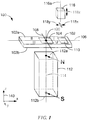
- a back-biased proximity sensor 100 is shown proximate to a ferromagnetic object 116, but does not include the ferromagnetic object 116.
- the back-biased proximity sensor 100 can include a substrate 102, for example, a semiconductor substrate, having first and second major surfaces 102a, 102b.
- the substrate 102 can include a substrate region 104.
- the substrate 102 can include one or more magnetic field sensing elements (not shown) disposed on or under the first surface 102a and inside of the substrate region 104.
- the substrate region 104 is shown to be square. However, in other embodiments, the substrate region 104 can be rectangular, oval, round, or any other planar shape defined by characteristics below.
- An electronic circuit 110 can be disposed in or on the first surface 102a and can be coupled to the magnetic field sensing element(s).
- the back-biased proximity sensor 100 can include a magnet 112 having first and second opposing surfaced 112a, 112b, respectively.
- a north pole, N can be disposed upon the first surface 112a and a south pole, S, can be disposed upon the second surface 112b.
- the north pole, N, and the south pole, S are reversed in position.
- a magnet axis 114 passes through the north and south poles.
- first and second orthogonal exes 106, 108 intersect the at a coordinate axis point 120.
- the coordinate axis point 120 can be at a geometric center the coordinate axis region 104.
- the magnetic axis 114 can intersect the coordinate axis point 120.
- the substrate region 104 is a region in which magnetic fields generated by the magnet 112 can be, in some embodiments, substantially perpendicular to the first surface 102a of the substrate 102. Further, outside of the substrate region 104, magnetic fields are not substantially perpendicular to the surface 102a.
- the substrate region 104 has a size and a shape
- the magnet 112 also has a size and shape, selected to provide that, when the ferromagnetic object 116 is not present, within the substrate region 104, the magnetic fields at the surface 102a of the substrate 102 are within about five degrees of perpendicular to the surface 102a, and outside of the substrate region 104, the magnetic fields are beyond about five degrees.
- the substrate region 104, and the magnet 112 can have other sizes and shapes to result in magnetic field lines with other angles within and outside of the substrate region, for example, within the substrate region 104 within less than about two degrees, within less than about five degrees, less than about ten, within less than about fifteen, within less than about twenty, within less than about twenty-five, within less than about thirty, within less than about thirty-five forty, or within less than about forty-five degrees.
- angles of magnetic field lines are greater than or equal to the above-described angles.
- a preferred magnetic field angle is zero or near zero.
- the back-biased proximity sensor 100 can be used to sense the ferromagnetic object 116 at different positions along directions 118z, 118x, 118z (see also Cartesian coordinates 140).
- the ferromagnetic object 116 can have a central axis 116a in a direction of a z-axis (see and the Cartesian coordinates 140) and the central axis 116a can intersect the coordinate axis point 120.
- the central axis 116a can intersect the substrate 102 anywhere within first, second, third, and fourth planar portions, here shown to be quadrants (I, II, III, IV).
- the direction 118x, 118y, 118z can be tangent to a movement line, which may or may not be a straight movement line.
- the direction 118x, 118y, 118z is perpendicular to the first surface 102a of the substrate 102, i.e., in a direction of the z-axis.
- other angles are also possible.
- Cartesian coordinates 140 are consistent among the various figures below, in which the surface 102a of the substrate is in an x-y plane.
- Quadrants I, II, III, IV are indicative of quadrants defined by the first and second axes 106, 108.
- the first and second axes 106, 108 are not orthogonal.
- the labels I, II, III, IV are indicative of so-called "planar portions.”
- the term "planar portion” applies to both four quadrants defined by two axes 106, 108 (and other similar axes in other figures) that are orthogonal, and also to four planar portions defined by two axes 106, 108 (and other similar axes in other figures) that are not orthogonal. Quadrants are used in descriptions herein for clarity.
- magnetic fields at magnetic field sensing elements within the substrate region 104 can be substantially perpendicular to the surface 102a of the substrate 102 when the ferromagnetic object 116 is not present.
- first surface 102a can be toward the ferromagnetic object 116 as shown, in other embodiments, the first surface 102a can be toward the magnet 112.
- a substrate 202 with a first surface 202a can be the same as or similar to the substrate 102 with the first surface 102a of FIG. 1 .
- a substrate region 216 with a coordinate axis point 234 can be the same as or similar to the substrate region 104 with the coordinate axis point 120 of FIG. 1 .
- An electronic circuit 214 can be the same as or similar to the electronic circuit 110 of FIG. 1 .
- a first coordinate axis 230 and a second coordinate axis 232 can be the same as or similar to first and second coordinate axes 106, 108, respectively, of FIG. 1 .
- Quadrants 1, 11, III, IV are indicative of quadrants defined by the first and second coordinate axes 230, 232 and are the same as or similar to the quadrants I, II, III, IV of FIG. 1 .
- the first and second coordinate axes can have any angle relative to the substrate 202.
- First, second, third and fourth vertical Hall elements 204, 206, 208, 210 can be disposed on, in, or over the first surface 202a of the substrate 202 and within the substrate region 216.
- Maximum response axes 204a, 206a of the first and second vertical Hall effect elements 204, 206, respectively, can be generally aligned with the first coordinate axis 230.
- Maximum response axes 208a, 210a of the third and fourth vertical Hall effect elements 208, 210, respectively, can be generally aligned with the second coordinate axis 232.
- Cartesian coordinates 240 show that the first surface 202a of the substrate 202 can be in the same x-y plane identified in FIG. 1 .
- the maximum response axes 204a, 206a, 208a, 210a of the magnetic field sensing elements 204, 206, 208, 210, respectively are shown to be aligned with first and second coordinate axes 230, 232, respectively, in other embodiments, the maximum response axes can be at other positions.
- the one vertical Hall effect element can be any one of the four vertical Hall effect elements.
- the one vertical Hall effect element can also be at another position within the substrate region 216, for example, at a center of the substrate region 216.
- the two vertical Hall effect elements can be any two of the four vertical Hall effect elements.
- the two vertical Hall effect elements can also be at other positions within the substrate region 216.
- the three vertical Hall effect elements can be any three of the four vertical Hall effect elements.
- the three vertical Hall effect elements can also be at other positions within the substrate region 216.
- the three vertical Hall elements can be physically arranged in a triangle.
- the four vertical Hall elements 204, 206, 208, 210 can be physically arranged in a square pattern (see, e.g., FIG. 9 ) rather than in an orthogonal cross pattern.
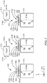
- a back-biased magnetic field sensor 300 is shown in three views as a ferromagnetic object 314 approaches in a direction 314a parallel to a z axis of Cartesian coordinates 340 and also moves in a direction 314b parallel to an x (and/or y) axis.
- the back-biased magnetic field sensor 300 can be the same as or similar to the magnetic field sensor 100 of FIG. 1 .
- the back-biased magnetic field sensor 300 can include a magnet 310 with a magnet axis 310a, which can be the same as or similar to the magnet 112 with the magnet axis 114 of FIG. 1 .
- the back-biased magnetic field sensor 300 can include a substrate 302 with a first surface 302a, which can be the same as or similar to the substrate 102 with the first surface 102a of FIG. 1 .
- Third, second, and fourth vertical Hall effect elements 304, 306, 308 can be the same as or similar to the third, second, and fourth vertical Hall effect elements 208, 206, 210 of FIG. 2 .
- a first vertical Hall effect element comparable to the first vertical Hall effect element 204 is not shown, for clarity.
- Magnetic field line 312a is representative of a magnetic field direction at the third vertical Hall effect element 304, and is only slightly tilted (e.g., substantially perpendicular) in a negative x direction in an x-z plane in Cartesian coordinates 340.
- Magnetic field line 312b is representative of a magnetic field direction at the second vertical Hall effect element 306, and is only slightly tilted (e.g., substantially perpendicular) in a positive y direction in a y-z plane in Cartesian coordinates 340.
- Magnetic field line 312c is representative of a magnetic field direction at the fourth vertical Hall effect element 308, and is only slightly tilted (e.g., substantially perpendicular) in a positive x direction in the x-z plane in Cartesian coordinates 340.
- the third, second, and fourth vertical Hall effect elements 304, 306, 308 of FIG. 3 have output signals that are nearly zero, since they have maximum response axes that are in the x-y plane, and since projections of the magnetic field lines 312a, 312b, 312c upon respective maximum response axes in the x-y plane to which the vertical Hall elements are sensitive (see, e.g., FIG. 2 ) are nearly zero.
- magnetic field lines 312d, 312e, 312f and magnetic field lines 312g, 312h, 312i are different and less vertical, i.e., less aligned with the z axis of the Cartesian coordinates 340. Accordingly, output signals from third, second, and fourth vertical Hall effect elements 304, 306, 308 change amplitude by different amounts and with different magnitude signs as the ferromagnetic object 314 approaches the magnetic field sensor 300 from different sides.
- the change in magnitudes and signs of the output signals can be detected to indicate not only a separation (or a separation threshold) associated with proximity of the ferromagnetic object 314 to the magnetic field sensor 300, but also from which side (or, in some embodiments, from which quadrant I, II, III, IV of FIG. 2 ) the ferromagnetic object 314 approaches.
- FIGS. 4-7 below show representative electronic circuits that can be used to detect the above-described proximity of the ferromagnetic object 314 to the magnetic field sensor 300 of FIG. 3 , having one, two, or four vertical Hall effect elements.
- circuits can be used that accomplish current spinning described above. However, in other embodiments, current spinning is not used.
- an electronic circuit 400 can be the same as or similar to the electronic circuit 214 of FIG. 2 , but using only one vertical Hall effect element, for example, the first vertical Hall element 204 of FIG. 2 . While it is indicated that the first vertical Hall effect element 204 is used with the electronic circuit 400, in other embodiments, the vertical Hall effect element that is used can be any one of the vertical Hall elements of FIG. 4 .
- the electronic circuit 400 can include an amplifier 404 coupled to receive a differential signal 402.
- the differential signal 402 can be coupled to a vertical Hall effect element.
- the amplifier 404 can generate an amplified signal 404a.
- a comparator circuit 410 can be coupled to receive the amplified signal 404a and coupled to receive a reference signal 414.
- the comparator circuit 410 can be configured to generate a comparison signal 410a having a first state indicative of the ferromagnetic object 314 of FIG. 3 being far away from the magnetic field sensor 300 and having a second different state indicative of the ferromagnetic object 314 being both closer to the magnetic field sensor 300 and also closer to a first two adjacent quadrants (e.g., I, IV) (see I, II, III, IV of FIG. 2 ) of the substrate 202 than to other quadrants.
- a first two adjacent quadrants e.g., I, IV
- a comparator circuit 420 can be coupled to receive the amplified signal 404a and coupled to receive a different reference signal 418.
- the comparator circuit 420 can be configured to generate a comparison signal 420a having a first state indicative of the ferromagnetic object 314 of FIG. 3 being far away from the magnetic field sensor 300 and having a second different state indicative of the ferromagnetic object 314 being both closer to the magnetic field sensor 300 and also closer to a second two adjacent quadrants (e.g., II, III) (see 1, II, III, IV of FIG. 2 ) of the substrate 202 than to other quadrants.
- a second two adjacent quadrants e.g., II, III
- the comparison signals 410a, 420a provide a nonlinear magnetic field sensor.
- the comparator circuits 410, 420 and other comparator circuits herein can be linear comparators. However, in other embodiments, the comparator circuits can be digital circuits configured to generate output signals having at least two different states.
- a position calculation module 412 can be coupled to the comparators 410, 420.
- the position calculation module 412 can be operable to generate a position signal 412a indicative of both proximity of the ferromagnetic object 314 and also on which side of an axis, e.g., on which side of the coordinate axis 232, the ferromagnetic object 314 is proximate.
- the electronic circuit 400 can be operable to identify both proximity and position of the ferromagnetic object 314.
- An output format module 416 can be coupled to receive the position signal 412a and can be configured to generate a formatted signal 416a indicative of the position signal 412a.
- the formatted signal 416a can be in one of a variety of signal formats, including, but not limited to, a PWM format, a SENT format, an I2C format, and a CAN format.
- the amplified signal 404a can be coupled to the position calculation module 412 and the position signal 412a can be indicative of a linear representation of a signed amplitude of the amplified signal 404a, which can provide a linear representation of both proximity and position (i.e., two quadrant localization) of the ferromagnetic object 314, either a continuous linear representation or a multi-step digital representation.
- an electronic circuit 500 can be the same as or similar to the electronic circuit 214 of FIG. 2 , but using two vertical Hall effect elements, for example, the first and second vertical Hall elements 204, 206, respectively, of FIG. 2 , physically arranged in parallel to each other. While it is indicated that the first and second vertical Hall effect elements 204, 206 are used with the electronic circuit 500, in other embodiments, the vertical Hall effect elements can be any two of the vertical Hall elements of FIG. 2 that are aligned along an axis.
- the electronic circuit 500 can include amplifiers 504, 516 coupled to receive differential signals 502, 514, respectively.
- the differential signals 502, 514 can be coupled to two respective vertical Hall effect elements.
- the amplifiers 504, 516 can generate amplified signals 504a, 516a.
- a summing circuit 506 can receive and sum the amplified signals 504a, 516a and can generate a summed signal 506a.
- a comparator circuit 508 can be coupled to receive the summed signal 506a and coupled to receive a reference signal 520.
- the comparator circuit 508 can be configured to generate a comparison signal 508a having a first state indicative of the ferromagnetic object 314 being far away from the magnetic field sensor 300 and having a second different state indicative of the ferromagnetic object 314 being both closer to the magnetic field sensor 300 and also closer to a first two adjacent quadrants (e.g., I, IV) (see I, II, III, IV of FIG. 2 ) of the substrate 202 than to other quadrants.
- a first two adjacent quadrants e.g., I, IV
- a comparator circuit 518 can be coupled to receive the summed signal 506a and coupled to receive a different reference signal 518.
- the comparator circuit 518 can be configured to generate a comparison signal 518a having a first state indicative of the ferromagnetic object 314 of FIG. 3 being far away from the magnetic field sensor 300 and having a second different state indicative of the ferromagnetic object 314 being both closer to the magnetic field sensor 300 and also closer to a second two adjacent quadrants (e.g., II, III) (see I, II, III, IV of FIG. 2 ) of the substrate 202 than to other quadrants.
- a second two adjacent quadrants e.g., II, III
- the comparison signals 510a, 518a provide a nonlinear magnetic field sensor.
- a position calculation module 510 can be the same as or similar to the position calculation module 412.
- An output format module 512 can be the same as or similar to the output format module 416 of FIG. 4
- the summed signal 506a can be coupled to the position calculation module 510 and the position signal 510a can be indicative of a linear representation of a signed amplitude of the summed signal 506a, which can provide a linear representation of both proximity and position (i.e., two of four quadrant localization) of the ferromagnetic object 314, either a continuous linear representation or a multi-step digital representation.
- an electronic circuit 600 can be the same as or similar to the electronic circuit 214 of FIG. 2 , but using two vertical Hall effect elements different than those of FIG. 5 , for example, the first and third vertical Hall elements 204, 208, respectively, of FIG. 2 , physically arranged at respective ninety degree angles to each other. While it is indicated that the first and third vertical Hall effect elements 204, 208 are used with the electronic circuit 600, in other embodiments, the vertical Hall effect elements can be any two of the vertical Hall elements of FIG. 2 that are arranged at angles to each other, e.g., ninety degrees.
- the electronic circuit 600 can include amplifiers 604, 618 coupled to receive differential signals 602, 616.
- the differential signals 602, 616 can be coupled to two respective vertical Hall effect elements.
- the amplifiers 604, 618 can generate amplified signals 604a, 618a.
- a comparator circuit 608 can be coupled to receive the amplified signal 604a and coupled to receive a reference signal 624.
- the comparator circuit 608 can be configured to generate a comparison signal 608a having a first state indicative of the ferromagnetic object 314 being far away from the magnetic field sensor 300 and having a second different state indicative of the ferromagnetic object 314 being both closer to the magnetic field sensor 300 and also closer to a first two adjacent quadrants (e.g., I, IV) (see I, II, III, IV of FIG. 2 ) of the substrate 202 then to other quadrants.
- a first two adjacent quadrants e.g., I, IV
- a comparator circuit 610 can be coupled to receive the amplified signal 604a and coupled to receive a different reference signal 626.
- the comparator circuit 610 can be configured to generate a comparison signal 610a having a first state indicative of the ferromagnetic object 314 of FIG. 3 being far away from the magnetic field sensor 300 and having a second different state indicative of the ferromagnetic object 314 being both closer to the magnetic field sensor 300 and also closer to a second two adjacent quadrants (e.g., II, III) (see I, II, III, IV of FIG. 2 ) of the substrate 202 than to other quadrants.
- a second two adjacent quadrants e.g., II, III
- a comparator circuit 620 can be coupled to receive the amplified signal 618a and coupled to receive a reference signal 628.
- the comparator circuit 620 can be configured to generate a comparison signal 620a having a first state indicative of the ferromagnetic object 314 being far away from the magnetic field sensor 300 and having a second different state indicative of the ferromagnetic object 314 being both closer to the magnetic field sensor 300 and also closer to a third two adjacent quadrants (e.g., I, II) (see I, II, III, IV of FIG. 2 ) of the substrate 202 then to other quadrants.
- a third two adjacent quadrants e.g., I, II
- a comparator circuit 622 can be coupled to receive the amplified signal 618a and coupled to receive a different reference signal 630.
- the comparator circuit 622 can be configured to generate a comparison signal 622a having a first state indicative of the ferromagnetic object 314 of FTG. 3 being far away from the magnetic field sensor 300 and having a second different state indicative of the ferromagnetic object 314 being both closer to the magnetic field sensor 300 and also closer to a fourth two adjacent quadrants (e.g., III, IV) (see I, II, III, IV of FIG. 2 ) of the substrate 202 than to other quadrants.
- a fourth two adjacent quadrants e.g., III, IV
- the magnetic field sensor 600 can identify one quadrant (e.g., IV) to which the ferromagnetic object 314 is closest.
- the comparison signals 608a, 610a, 620a, 622a can provide a nonlinear magnetic field sensor.
- a quadrant calculation module 612 can be similar to the position calculation module 412 of FIG. 4 . However, the quadrant calculation module 612 can generate a quadrant signal 612a that can localize the position of the ferromagnetic object 314 to be within a single quadrant.
- An output format module 614 can be similar to the output format module 416 of FIG. 4 .
- the amplified signal 604a and the amplified signal 618a can be coupled to the position calculation module 612 and the position signal 612a can be indicative of a linear representation of signed amplitudes of the amplified signals 604a, 618a, which can provide a linear representation of both proximity and position (i.e., one of four quadrant localization) of the ferromagnetic object 314, either a continuous linear representation or a multi-step digital representation.
- an electronic circuit 700 can be the same as or similar to the electronic circuit 214 of FIG. 2 , but using a four vertical Hall effect elements, for example, the first, second, third and fourth vertical Hall elements 204, 206, 208, 210 respectively, of FIG. 2 . While it is indicated that the first and second vertical Hall effect elements 204, 206 are aligned along the second coordinate axis 232 and the third and fourth vertical Hall effect element 208, 210 are aligned along the first coordinate axis 230, in other embodiments, the vertical Hall effect elements can have a different alignment.
- the electronic circuit 700 can include amplifiers 704, 720 coupled to receive differential signals 702, 718.
- the differential signals 702, 718 can be coupled to two respective vertical Hall effect elements, e.g., first and second vertical Hall effect elements 204, 206 respectively, of FIG. 2 , which can be physically arranged in parallel.
- the amplifiers 704, 720 can generate amplified signals 704a, 720a.
- a summing circuit 706 can receive and sum the amplified signals 704a, 720a and can generate a summed signal 706a.
- a comparator circuit 708 can be coupled to receive the summed signal 706a and coupled to receive a reference signal 736.
- the comparator circuit 708 can be configured to generate a comparison signal 708a having a first state indicative of the ferromagnetic object 314 being far away from the magnetic field sensor 300 and having a second different state indicative of the ferromagnetic object 314 being both closer to the magnetic field sensor 300 and also closer to a first two adjacent quadrants (e.g., I, IV) (see I, II, III, IV of FIG. 2 ) of the substrate 202 than to other quadrants.
- a first two adjacent quadrants e.g., I, IV
- a comparator circuit 710 can be coupled to receive the summed signal 706a and coupled to receive a different reference signal 738.
- the comparator circuit 710 can be configured to generate a comparison signal 710a having a first state indicative of the ferromagnetic object 314 of FIG. 3 being far away from the magnetic field sensor 300 and having a second different state indicative of the ferromagnetic object 314 being both closer to the magnetic field sensor 300 and also closer to a second two adjacent quadrants (e.g., II, III) (see I, II, III, IV of FIG. 2 ) of the substrate 202 than to other quadrants.
- a second two adjacent quadrants e.g., II, III
- the electronic circuit 700 can include amplifiers 724, 732 coupled to receive differential signals 722, 730.
- the differential signals 722, 730 can be coupled to two respective vertical Hall effect elements, e.g., third and fourth vertical Hall effect elements 208, 210, respectively, of FIG. 2 , which can be physically arranged in parallel but at an angle, for example ninety degrees, relative to the first and second vertical Hall elements 204, 206.
- the amplifiers 724, 732 can generate amplified signals 724a, 732a.
- a summing circuit 726 can receive and sum the amplified signals 724a, 732a and can generate a summed signal 726a.
- a comparator circuit 728 can be coupled to receive the summed signal 726a and coupled to receive a reference signal 740.
- the comparator circuit 728 can be configured to generate a comparison signal 728a having a first state indicative of the ferromagnetic object 314 being far away from the magnetic field sensor 300 and having a second different state indicative of the ferromagnetic object 314 being both closer to the magnetic field sensor 300 and also closer to a third two adjacent quadrants (e.g., I, II) (see I, II, III, IV of FIG. 2 ) of the substrate 202 than to other quadrants.
- a third two adjacent quadrants e.g., I, II
- a comparator circuit 734 can be coupled to receive the summed signal 726a and coupled to receive a different reference signal 742.
- the comparator circuit 734 can be configured to generate a comparison signal 734a having a first state indicative of the ferromagnetic object 314 of FIG. 3 being far away from the magnetic field sensor 300 and having a second different state indicative of the ferromagnetic object 314 being both closer to the magnetic field sensor 300 and also closer to a fourth two adjacent quadrants (e.g., III, IV) (see I, II, III, IV of FIG. 2 ) of the substrate 202 than to other quadrants.
- a fourth two adjacent quadrants e.g., III, IV
- the magnetic field sensor 700 can identify one quadrant (e.g., IV) to which the ferromagnetic object 314 is closest.
- the comparison signals 708a, 710a, 728a, 734a can provide a nonlinear magnetic field sensor.
- a quadrant calculation module 712 can be similar to the position calculation module 412 of FIG. 4 . However, the quadrant calculation module 712 can generate a quadrant signal 712a that can localize the position of the ferromagnetic object 314 to be within a single quadrant.
- An output format module 714 can be similar to the output format module 416 of FIG. 4 .
- the summed signal 706a and the summed signal 726a can be coupled to the quadrant calculation module 712 and the position signal 712a can be indicative of a linear representation of signed amplitudes of the summed signals 704a, 718a, which can provide a linear representation of both proximity and position (i.e., one quadrant localization) of the ferromagnetic object 314, either a continuous linear representation or a multi-step digital representation.
- each one of the vertical Hall effect elements can be replaced by one or more magnetoresistance elements. It will be understood that a both a vertical Hall effect element and a magnetoresistance element have maximum response axes parallel to a substrate upon which they are disposed.
- magnetoresistance elements can be used in bridge arrangements.
- a magnetoresistance element bridge 800 can use a magnetoresistance element 802 indicative of any one of the vertical Hall effect elements 204, 206, 208, 210, respectively, of FIG. 2 .
- the magnetoresistance elements 802 can be coupled in a bridge arrangement to fixed resistors 804, 806, 808.
- a differential signal 812, 814 can be coupled to an amplifier 816 to generate and amplified signal 816a.
- the amplifier 816 can be the same as or similar to any of the amplifiers of FIGS. 4-7 .
- magnetoresistance elements can be used as any of the above-described vertical Hall effect elements.
- a substrate 902 with a first surface 902a can be the same as or similar to the substrate 102 with the first surface 109a of FIG. 1 .
- a substrate region 916 with a coordinate axis point 934 can be the same as or similar to the substrate region 104 with the coordinate axis point 120 of FIG. 1 .
- An electronic circuit 914 can be the same as or similar to the electronic circuit 110 of FIG. 1 .
- a first coordinate axis 930 and a second coordinate axis 932 can be the same as or similar to first and second coordinate axes 106, 108, respectively, of FIG. 1 .
- Quadrants I, II, III, IV are indicative of quadrants defined by the first and second coordinate axes 930, 932 and are the same as or similar to the quadrants I, II, III, IV of FIG. 1 .
- the first and second coordinate axes 930, 932 can have any angle relative to the substrate 902.
- First, second, third and fourth vertical Hall elements 904, 906, 908, 910 can be disposed on, in, or over the first surface 902a of the substrate 902 and within the substrate region 916.
- Maximum response axes 904a, 906a of the first and second vertical Hall effect elements 904, 906, respectively, can be generally aligned with the first coordinate axis 930.
- Maximum response axes 908a, 910a of the third and fourth vertical Hall effect elements 908, 910, respectively, can be generally aligned with the second coordinate axis 932.
- Cartesian coordinates 940 show that the first surface 902a of the substrate 902 can be in the same x-y plane identified in FIG. 1 .
- the maximum response axes 904a, 906a, 908a, 910a of the magnetic field sensing elements 904, 906, 908, 910, respectively are shown to be aligned with first and second coordinate axes 930, 932, respectively, in other embodiments, the maximum response axes can be at other positions.
- the one vertical Hall effect element can be any one of the four vertical Hall effect elements.
- the one vertical Hall effect element can also be at another position within the substrate region 916, for example, at a center of the substrate region 916.
- the two vertical Hall effect elements can be any two of the four vertical Hall effect elements.
- the two vertical Hall effect elements can also be at other positions within the substrate region 916.
- the three vertical Hall effect elements can be any three of the four vertical Hall effect elements.
- the three vertical Hall effect elements can also be at other positions within the substrate region 916.
- a back-biased magnetic field sensor 1000 is shown in three views as a ferromagnetic object 1014 approaches in a direction 1014a parallel to a z axis of Cartesian coordinates 1040 and also moves in a direction 1014b parallel to an x (and/or y) axis.
- the back-biased magnetic field sensor 1000 can be the same as or similar to the magnetic field sensor 100 of FIG. 1 .
- the back-biased magnetic field sensor 1000 can include a magnet 1010 with a magnet axis 1010a, which can be the same as or similar to the magnet 112 with the magnet axis 114 of FIG. 1 .
- the back-biased magnetic field sensor 1000 can include a substrate 1002 with a first surface 1002a, which can be the same as or similar to the substrate 102 with the first surface 102a of FIG. 1 .
- First, fourth, and second vertical Hall effect elements 1004, 1006, 1008 can be the same as or similar to the First, fourth, and second vertical Hall effect elements 904, 910, 906of FIG. 9 .
- a third vertical Hall effect element comparable to the third vertical Hall effect element 908 is not shown, for clarity.
- Magnetic field line 1012a is representative of a magnetic field direction at the first vertical Hall effect element 1004, and is only slightly tilted (e.g., substantially perpendicular) in a negative x direction in an x-z plane in Cartesian coordinates 1040.
- Magnetic field line 1012b is representative of a magnetic field direction at the fourth vertical Hall effect element 1006, and is only slightly tilted (e.g., substantially perpendicular) in a positive y direction in a y-z plane in Cartesian coordinates 1040.
- Magnetic field line 1012c is representative of a magnetic field direction at the second vertical Hall effect element 1008, and is only slightly tilted (e.g., substantially perpendicular) in a positive x direction in the x-z plane in Cartesian coordinates 1040.
- the first, fourth, and second vertical Hall effect elements 1004, 1006, 1008 of FIG. 10 have output signals that are nearly zero, since they have maximum response axes that are in the x-y plane, and since projections of the magnetic field lines 1012a, 1012b, 1012c upon respective maximum response axes in the x-y plane to which the vertical Hall elements are sensitive (see, e.g., FIG. 9 ) are nearly zero.
- magnetic field lines 1012d, 1012e, 1012f and magnetic field lines 1012g, 1012h, 1012i are different and less vertical, i.e., less aligned with the z axis of the Cartesian coordinates 1040. Accordingly, output signals from the first, fourth, and second vertical Hall effect elements 1004, 1006, 1008 change amplitude by different amounts and with different magnitude signs as the ferromagnetic object 1014 approaches the magnetic field sensor 1000 from different sides.
- the change in magnitudes and signs of the output signals can be detected to indicate not only a separation (or a separation threshold) associated with proximity of the ferromagnetic object 1014 to the magnetic field sensor 1000, but also from which side (or, in some embodiments, from which quadrant I, II, III, IV of FIG. 9 ) the ferromagnetic object 1014 approaches.
- the electronic circuit 914 of FIG. 9 can be the same as or similar to the electronic circuits of FIGS. 4-7 for different number of vertical Hail effect elements.
- the four vertical Hall effect elements 904, 906, 908, 910 can also be arranged in a circle, with four vertical Hall effect elements, or with fewer than or more than four vertical Hall effect elements.
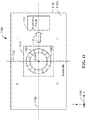
- a circular vertical Hall (CVH0 sensing element can be used as described below in conjunction with FIG. 11 .
- a substrate 1102 with a first surface 1102a can be the same as or similar to the substrate 102 with the first surface 102a of FIG. 1 .
- a substrate region 1116 with a coordinate axis point 1134 can be the same as or similar to the substrate region 104 with the coordinate axis point 120 of FIG. 1 .
- An electronic circuit 1114 can be the same as or similar to the electronic circuit 110 of FIG. 1 .
- a first coordinate axis 1130 and a second coordinate axis 1132 can be the same as or similar to first and second coordinate axes 106, 108, respectively, of FIG. 1 .
- Quadrants I, II, III, IV are indicative of quadrants defined by the first and second coordinate axes 1130, 1132 and are the same as or similar to the quadrants I, II, III, IV of FIG. 1 .
- the first and second coordinate axes 1130, 1132 can have any angle relative to the substrate 1102.
- a plurality of vertical Hall elements arranged as a circular vertical Hall (CVH) sensing element 1104 can be disposed on, in, or over the first surface 1102a of the substrate 1102 and within the substrate region 1116. Maximum response axes of the CVH sensing element 1104 can be parallel to an x-y plane of the first surface 1102 of the substrate 1102.
- CVH circular vertical Hall
- a CVH sensing element comprises a plurality of overlapping vertical Hall elements (i.e.. overlapping sets of electrical contacts) arranged over a common circular implant and diffusion region without diffused barriers between the plurality of vertical Hall elements.
- the plurality of vertical Hall elements can be sequentially driven, for example, one at a time, and sequential signals can be generated from the plurality of vertical Hal elements on a common signal path.
- the sequential signals are indicative of sequential analog signal samples, each sample from one of the vertical Hall elements.
- CVH sensing elements have thirty-two or sixty-four electrical contacts, and therefore, thirty-two or sixty-four vertical Hall elements. However, other numbers of electrical contacts can result in a CVH sensing element with more than thirty-two (or more than sixty-four) or fewer than thirty-two (or fewer than thirty-two) vertical Hall elements.
- each one of the vertical Hall elements in the CVH sensing element can generate a sample having a sample value indicative of a magnitude of a magnetic field as projected upon the x-y plane.
- the sample values can be indicative of a proximity of and a position of a ferromagnetic object in much the same way as described above in conjunction with FIGS. 9 and 10 .
- the signal samples can be digitized and a processor can analyze the signal values to determine the above.
- CVH sensing elements are described in more detail in conjunction with U.S. Patent No. 8,729,890, issued May 20, 2014 , with patent is incorporated herein in its entirety.
- CVH sensing elements are not used in a back-biased arrangement described herein, but instead with a magnet that has a magnetic direction parallel to the surface 1102a of the substrate 1102.
Claims (24)
- Magnetfeldsensor zum Erfassen einer Bewegung eines ferromagnetischen Gegenstands (116) entlang einer Bahn, wobei der Magnetfeldsensor Folgendes umfasst:einen Magneten (112);ein Halbleitersubstrat (102) nah bei dem Magneten (112) und in einer Lage zwischen dem ferromagnetischen Gegenstand (116) und dem Magneten (112), wobei das Halbleitersubstrat (102) Folgendes umfasst:eine erste und eine zweite Substratachse (106, 108) auf einer Oberfläche des Halbleitersubstrats (102), die einander in einem Substratachsenpunkt schneiden, um dadurch das Halbleitersubstrat in vier ebene Abschnitte in einer Ebene der Substratachsen zu teilen, wobei die erste Substratachse (106) die Ebene der Substratachsen in eine erstes Paar komplementärer Halbebenen auf gegenüberliegenden Seiten der ersten Substratachse (106) teilt und die zweite Substratachse (108) die Ebene der Substratachsen in ein zweites Paar komplementärer Halbebenen auf gegenüberliegenden Seiten der zweiten Substratachse (108) teilt; undeinen Substratbereich (104) auf der Oberfläche des Halbleitersubstrats (102), wobei der Substratbereich (104) nah bei dem Substratachsenpunkt liegt und diesen umgibt, wobei von dem Magneten (112) an dem Substratbereich (104) erzeugte Magnetfelder in Abwesenheit des ferromagnetischen Gegenstands (116) im Wesentlichen senkrecht zu dem Halbleitersubstrat (102) sind, wobei der Magnetfeldsensor ferner Folgendes umfasst:eine erstes Magnetfelderfassungselement (204), das auf oder unter der Oberfläche des Halbleitersubstrats (102) angeordnet ist und in dem Substratbereich (104) angeordnet ist, wobei das erste Magnetfelderfassungselement (204) eine im Wesentlichen zu der ersten Substratachse (106) parallele Achse maximaler Empfindlichkeit umfasst, wobei ein Mittelpunkt des ersten Magnetfelderfassungselements (204) auf der zweiten Substratachse (108) angeordnet ist; undeine elektronische Schaltung (110), die auf oder unter der Oberfläche des Halbleitersubstrats (102) angeordnet ist, an das erste Magnetfelderfassungselement (204) gekoppelt ist und dazu konfiguriert ist, auf der Basis von Betrag und Vorzeichen eines Ausgangssignals des Magnetfelderfassungselements ein Lagesignal mit einer Vielzahl von Zuständen zu erzeugen, wobei der Zustand des Lagesignals angibt, dass der ferromagnetische Gegenstand (116) um mehr oder weniger als eine vorgegebene Entfernung von dem Magnetfeldsensor entfernt ist, und wobei, falls der ferromagnetische Gegenstand um weniger als die vorgegebene Entfernung entfernt ist, der Zustand ferner angibt, ob der ferromagnetische Gegenstand (116) näher an den in einer ersten des zweiten Paars komplementärer Halbebenen liegenden ebenen Abschnitten des Substrats liegt oder näher an den in einer zweiten des zweiten Paars komplementärer Halbebenen liegenden ebenen Abschnitten liegt.
- Magnetfeldsensor nach Anspruch 1, wobei die elektronische Schaltung (110) ferner dazu konfiguriert ist, ein Zweizustands-Vergleichssignal zu erzeugen, das einen Zustandswechsel aufweist, wenn sich der ferromagnetische Gegenstand (116) näher als eine vorgegebene Entfernung an das Halbleitersubstrat (102) bewegt.
- Magnetfeldsensor nach Anspruch 1, wobei das erste Magnetfelderfassungselement (204) ein vertikales Hall-Effekt-Element umfasst.
- Magnetfeldsensor nach Anspruch 1, wobei das erste Magnetfelderfassungselement (204) ein Magnetowiderstandselement umfasst.
- Magnetfeldsensor nach Anspruch 1, der ferner Folgendes umfasst:
ein zweites Magnetfelderfassungselement, das auf oder unter der Oberfläche des Halbleitersubstrats (102) angeordnet ist und in dem Substratbereich angeordnet ist, wobei das zweite Magnetfelderfassungselement eine im Wesentlichen zu der Achse maximaler Empfindlichkeit des ersten Magnetfelderfassungselement parallele Achse maximaler Empfindlichkeit umfasst. - Magnetfeldsensor nach Anspruch 5, wobei ein Mittelpunkt des zweiten Magnetfelderfassungselements auf der zweiten Substratachse (108) und nicht auf dem Substratachsenpunkt angeordnet ist.
- Magnetfeldsensor nach Anspruch 6, wobei die Mittelpunkte des ersten und des zweiten Magnetfelderfassungselements im Wesentlichen gleich weit von dem Substratachsenpunkt entfernt sind und auf gegenüberliegenden Seiten davon liegen.
- Magnetfeldsensor nach Anspruch 5, wobei die elektronische Schaltung (110) außerdem an das zweite Magnetfelderfassungselement gekoppelt ist, wobei die elektronische Schaltung ferner dazu konfiguriert ist, ein Zweizustands-Vergleichssignal zu erzeugen, das einen Zustandswechsel aufweist, wenn sich der ferromagnetische Gegenstand (116) näher als um die vorgegebene Entfernung an das Halbleitersubstrat (102) bewegt.
- Magnetfeldsensor nach Anspruch 5, wobei die elektronische Schaltung (110) außerdem an das zweite Magnetfelderfassungselement gekoppelt ist.
- Magnetfeldsensor nach Anspruch 5, der ferner Folgendes umfasst:ein drittes Magnetfelderfassungselement, das auf oder unter der Oberfläche des Halbleitersubstrats (102) angeordnet ist und in dem Substratbereich angeordnet ist, wobei das dritte Magnetfelderfassungselement eine zu der Achse maximaler Empfindlichkeit des ersten Magnetfelderfassungselements nicht parallele Achse maximaler Empfindlichkeit umfasst; undein viertes Magnetfelderfassungselement, das auf oder unter der Oberfläche des Halbleitersubstrats angeordnet ist und in dem Substratbereich angeordnet ist, wobei das vierte Magnetfelderfassungselement eine zu der Achse maximaler Empfindlichkeit des ersten Magnetfelderfassungselements nicht parallele Achse maximaler Empfindlichkeit umfasst.
- Magnetfeldsensor nach Anspruch 10, wobei der Mittelpunkt des ersten Magnetfelderfassungselements (204) auf der zweiten Substratachse (108) angeordnet ist, wobei ein Mittelpunkt des zweiten Magnetfelderfassungselements auf der zweiten Substratachse angeordnet ist, wobei ein Mittelpunkt des dritten Magnetfelderfassungselements auf der ersten Substratachse und nicht auf dem Substratachsenpunkt angeordnet ist, wobei ein Mittelpunkt des vierten Magnetfelderfassungselements auf der ersten Substratachse und nicht auf dem Substratachsenpunkt angeordnet ist.
- Magnetfeldsensor nach Anspruch 11, wobei die Mittelpunkte des ersten und des zweiten Magnetfelderfassungselements im Wesentlichen gleich weit von dem Substratachsenpunkt entfernt sind und auf gegenüberliegenden Seiten davon liegen, und wobei die Mittelpunkte des dritten und des vierten Magnetfelderfassungselements im Wesentlichen gleich weit von dem Substratachsenpunkt entfernt sind und auf gegenüberliegenden Seiten davon liegen.
- Magnetfeldsensor nach Anspruch 10, wobei es sich bei dem ersten, dem zweiten, dem dritten und dem vierten Magnetfelderfassungselement um vertikale Hall-Elemente mit einem Circular-Vertical-Hall(CVH)-Erfassungselement handelt.
- Magnetfeldsensor nach Anspruch 10, wobei die elektronische Schaltung (110) außerdem an das dritte und das vierte Magnetfelderfassungselement gekoppelt ist und dazu konfiguriert ist, ein Zweizustands-Vergleichssignal zu erzeugen, das einen ausgewählten Zustandswechsel aufweist, wenn sich der ferromagnetische Gegenstand (116) näher als um die vorgegebene Entfernung an das Halbleitersubstrat (102) bewegt.
- Magnetfeldsensor nach Anspruch 10, wobei die elektronische Schaltung (110) ferner an das zweite, das dritte und das vierte Magnetfelderfassungselement gekoppelt ist und wobei jeder Zustand ferner angibt, welchem der vier ebenen Abschnitte der ferromagnetische Gegenstand (116) am nächsten liegt.
- Magnetfeldsensor nach Anspruch 10, wobei das erste, das zweite, das dritte und das vierte Magnetfelderfassungselement vertikale Hall-Effekt-Elemente umfassen.
- Magnetfeldsensor nach Anspruch 10, wobei das erste, das zweite, das dritte und das vierte Magnetfelderfassungselement Magnetowiderstandselemente umfassen.
- Magnetfeldsensor nach Anspruch 1, der ferner Folgendes umfasst:
ein zweites Magnetfelderfassungselement, das auf oder unter der Oberfläche des Halbleitersubstrats (102) angeordnet ist und in dem Substratbereich angeordnet ist, wobei das zweite Magnetfelderfassungselement eine im Wesentlichen zu der Achse maximaler Empfindlichkeit des ersten Magnetfelderfassungselement senkrechte Achse maximaler Empfindlichkeit umfasst. - Magnetfeldsensor nach Anspruch 18, wobei ein Mittelpunkt des zweiten Magnetfelderfassungselements auf der ersten Substratachse (106) angeordnet ist und wobei die Mittelpunkte des ersten und des zweiten Magnetfelderfassungselements im Wesentlichen gleich weit von dem Substratachsenpunkt entfernt sind und nicht auf dem Substratachsenpunkt liegen.
- Magnetfeldsensor nach Anspruch 18, wobei die elektronische Schaltung (110) außerdem an das zweite Magnetfelderfassungselement gekoppelt ist, wobei die elektronische Schaltung ferner dazu konfiguriert ist, ein Zweizustands-Vergleichssignal zu erzeugen, das einen Zustandswechsel aufweist, wenn sich der ferromagnetische Gegenstand (116) näher als um die vorgegebene Entfernung an das Halbleitersubstrat (102) bewegt.
- Magnetfeldsensor nach Anspruch 18, wobei die elektronische Schaltung (110) außerdem an das zweite Magnetfelderfassungselement gekoppelt ist und wobei jeder Zustand ferner angibt, welchem der vier ebenen Abschnitte der ferromagnetische Gegenstand (116) am nächsten liegt.
- Magnetfeldsensor nach Anspruch 5 oder 18, wobei das erste und das zweite Magnetfelderfassungselement vertikale Hall-Effekt-Elemente umfassen.
- Magnetfeldsensor nach Anspruch 5 oder 18, wobei das erste und das zweite Magnetfelderfassungselement Mangnetowiderstandselemente umfassen.
- Magnetfeldsensor nach Anspruch 1, 5 oder 10, wobei das Lagesignal ein digitales Signal umfasst.
Applications Claiming Priority (2)
| Application Number | Priority Date | Filing Date | Title |
|---|---|---|---|
| US15/176,668 US10215590B2 (en) | 2016-06-08 | 2016-06-08 | Magnetic field sensor for sensing a proximity and/or a location of an object |
| PCT/US2017/033530 WO2017213824A1 (en) | 2016-06-08 | 2017-05-19 | Magnetic field sensor for sensing a proximity and/or a location of an object |
Publications (2)
| Publication Number | Publication Date |
|---|---|
| EP3469314A1 EP3469314A1 (de) | 2019-04-17 |
| EP3469314B1 true EP3469314B1 (de) | 2021-04-07 |
Family
ID=58794223
Family Applications (1)
| Application Number | Title | Priority Date | Filing Date |
|---|---|---|---|
| EP17726478.5A Active EP3469314B1 (de) | 2016-06-08 | 2017-05-19 | Magnetfeldsensor zur erfassung einer nähe und/oder eines standorts eines objekts |
Country Status (3)
| Country | Link |
|---|---|
| US (1) | US10215590B2 (de) |
| EP (1) | EP3469314B1 (de) |
| WO (1) | WO2017213824A1 (de) |
Families Citing this family (12)
| Publication number | Priority date | Publication date | Assignee | Title |
|---|---|---|---|---|
| US9810519B2 (en) | 2013-07-19 | 2017-11-07 | Allegro Microsystems, Llc | Arrangements for magnetic field sensors that act as tooth detectors |
| US9823092B2 (en) | 2014-10-31 | 2017-11-21 | Allegro Microsystems, Llc | Magnetic field sensor providing a movement detector |
| US10866117B2 (en) * | 2018-03-01 | 2020-12-15 | Allegro Microsystems, Llc | Magnetic field influence during rotation movement of magnetic target |
| DE102018112398A1 (de) * | 2018-05-23 | 2019-11-28 | Guboa Technology Co., Ltd | Vorrichtung zur Erfassung einer linearen Verschiebung |
| DE102018210595A1 (de) * | 2018-06-28 | 2020-01-02 | Infineon Technologies Ag | Sensorvorrichtungen und Verfahren zur Herstellung von Sensorvorrichtungen |
| US11255700B2 (en) | 2018-08-06 | 2022-02-22 | Allegro Microsystems, Llc | Magnetic field sensor |
| US10837753B2 (en) | 2019-01-10 | 2020-11-17 | Allegro Microsystems, Llc | Magnetic field sensor using MR elements for detecting flux line divergence |
| JP7260321B2 (ja) * | 2019-02-15 | 2023-04-18 | エイブリック株式会社 | 磁気センサ回路 |
| US11385075B2 (en) | 2020-02-21 | 2022-07-12 | Allegro Microsystems, Llc | Orientation independent magnetic field sensor |
| US11608109B2 (en) * | 2020-08-12 | 2023-03-21 | Analog Devices International Unlimited Company | Systems and methods for detecting magnetic turn counter errors with redundancy |
| US11733316B2 (en) * | 2020-12-14 | 2023-08-22 | Allegro Microsystems, Llc | Position sensor having harmonic distortion compensation |
| US11630168B2 (en) | 2021-02-03 | 2023-04-18 | Allegro Microsystems, Llc | Linear sensor with dual spin valve element having reference layers with magnetization directions different from an external magnetic field direction |
Family Cites Families (33)
| Publication number | Priority date | Publication date | Assignee | Title |
|---|---|---|---|---|
| JPS5613244B2 (de) | 1974-07-31 | 1981-03-27 | ||
| DE3122376A1 (de) | 1981-06-05 | 1982-12-23 | Robert Bosch Gmbh, 7000 Stuttgart | Vorrichtung zur erfassung der drehzahl von rotierenden teilen |
| US5045920A (en) * | 1990-06-28 | 1991-09-03 | Allegro Microsystems, Inc. | Dual-Hall ferrous-article-proximity sensor |
| US5304926A (en) | 1992-04-08 | 1994-04-19 | Honeywell Inc. | Geartooth position sensor with two hall effect elements |
| US5341097A (en) | 1992-09-29 | 1994-08-23 | Honeywell Inc. | Asymmetrical magnetic position detector |
| WO1997006404A2 (en) | 1995-08-02 | 1997-02-20 | Durakool Inc | Gear tooth sensor with improved resolution and stability |
| US6525531B2 (en) | 1996-01-17 | 2003-02-25 | Allegro, Microsystems, Inc. | Detection of passing magnetic articles while adapting the detection threshold |
| US5896030A (en) | 1996-10-09 | 1999-04-20 | Honeywell Inc. | Magnetic sensor with components attached to transparent plate for laser trimming during calibration |
| US6278269B1 (en) | 1999-03-08 | 2001-08-21 | Allegro Microsystems, Inc. | Magnet structure |
| JP2002372416A (ja) * | 2001-04-09 | 2002-12-26 | Nagano Fujitsu Component Kk | センサユニット |
| JP4855603B2 (ja) * | 2001-08-01 | 2012-01-18 | 富士通コンポーネント株式会社 | 加速度検出装置 |
| DE10210184A1 (de) | 2002-03-07 | 2003-09-18 | Philips Intellectual Property | Anordnung zum Bestimmen der Position eines Bewegungsgeberelements |
| US7199579B2 (en) | 2004-03-08 | 2007-04-03 | Allegro Microsystems, Inc. | Proximity detector |
| WO2005088259A1 (de) | 2004-03-11 | 2005-09-22 | Robert Bosch Gmbh | Magnetsensoranordnung |
| DE102004017191B4 (de) | 2004-04-07 | 2007-07-12 | Infineon Technologies Ag | Vorrichtung und Verfahren zur Ermittlung einer Richtung eines Objekts |
| US7365530B2 (en) | 2004-04-08 | 2008-04-29 | Allegro Microsystems, Inc. | Method and apparatus for vibration detection |
| US7112957B2 (en) * | 2004-06-16 | 2006-09-26 | Honeywell International Inc. | GMR sensor with flux concentrators |
| US7253614B2 (en) | 2005-03-21 | 2007-08-07 | Allegro Microsystems, Inc. | Proximity detector having a sequential flow state machine |
| US7915886B2 (en) * | 2007-01-29 | 2011-03-29 | Honeywell International Inc. | Magnetic speed, direction, and/or movement extent sensor |
| EP2000813A1 (de) | 2007-05-29 | 2008-12-10 | Ecole Polytechnique Fédérale de Lausanne | Magnetfeldsensor zum Messen der Richtung eines Magnetfelds |
| DE102007041230B3 (de) * | 2007-08-31 | 2009-04-09 | Fraunhofer-Gesellschaft zur Förderung der angewandten Forschung e.V. | Kalibrierbarer mehrdimensionaler magnetischer Punktsensor sowie entsprechendes Verfahren und Computerprogramm dafür |
| JP5324388B2 (ja) | 2009-10-15 | 2013-10-23 | 株式会社東海理化電機製作所 | 近接センサ |
| US8729892B2 (en) * | 2011-04-01 | 2014-05-20 | Allegro Microsystems, Llc | Differential magnetic field sensor structure for orientation independent measurement |
| US8729890B2 (en) | 2011-04-12 | 2014-05-20 | Allegro Microsystems, Llc | Magnetic angle and rotation speed sensor with continuous and discontinuous modes of operation based on rotation speed of a target object |
| US9575120B2 (en) | 2013-03-29 | 2017-02-21 | International Business Machines Corporation | Scan chain processing in a partially functional chip |
| WO2014189733A1 (en) | 2013-05-24 | 2014-11-27 | Allegro Microsystems, Llc | Magnetic field sensor for detecting a magnetic field in any direction above thresholds |
| US9733106B2 (en) | 2013-05-24 | 2017-08-15 | Allegro Microsystems, Llc | Magnetic field sensor to detect a magnitude of a magnetic field in any direction |
| US9982989B2 (en) * | 2013-07-17 | 2018-05-29 | Infineon Technologies Ag | Angle sensors, systems and methods |
| DE202014004425U1 (de) | 2014-04-28 | 2014-09-12 | Infineon Technologies Ag | Halleffekt-Sensoranordnung |
| US9852832B2 (en) * | 2014-06-25 | 2017-12-26 | Allegro Microsystems, Llc | Magnetic field sensor and associated method that can sense a position of a magnet |
| DE102014010547B4 (de) | 2014-07-14 | 2023-06-07 | Albert-Ludwigs-Universität Freiburg | Hallsensor |
| US9719806B2 (en) | 2014-10-31 | 2017-08-01 | Allegro Microsystems, Llc | Magnetic field sensor for sensing a movement of a ferromagnetic target object |
| US9823092B2 (en) | 2014-10-31 | 2017-11-21 | Allegro Microsystems, Llc | Magnetic field sensor providing a movement detector |
-
2016
- 2016-06-08 US US15/176,668 patent/US10215590B2/en active Active
-
2017
- 2017-05-19 EP EP17726478.5A patent/EP3469314B1/de active Active
- 2017-05-19 WO PCT/US2017/033530 patent/WO2017213824A1/en unknown
Non-Patent Citations (1)
| Title |
|---|
| None * |
Also Published As
| Publication number | Publication date |
|---|---|
| WO2017213824A1 (en) | 2017-12-14 |
| US20170356762A1 (en) | 2017-12-14 |
| EP3469314A1 (de) | 2019-04-17 |
| US10215590B2 (en) | 2019-02-26 |
Similar Documents
| Publication | Publication Date | Title |
|---|---|---|
| EP3469314B1 (de) | Magnetfeldsensor zur erfassung einer nähe und/oder eines standorts eines objekts | |
| US10837800B2 (en) | Arrangements for magnetic field sensors that act as movement detectors | |
| KR102176106B1 (ko) | 물체의 이동을 감지하는 센서 및 물체의 이동을 감지하는 방법 | |
| US9880026B1 (en) | Magnetic field sensor for detecting motion of an object | |
| EP3469313B1 (de) | Magnetfeldsensor zur erfassung der nähe eines objekts | |
| EP3623765B1 (de) | Winkelmagnetfeldsensor und rotierendes ziel mit streufeldimmunität | |
| US11313700B2 (en) | Magnetic field influence during rotation movement of magnetic target | |
| EP3469315B1 (de) | Anordnungen für magnetfeldsensoren zur annulierung von versatzvariationen | |
| US10670425B2 (en) | System for measuring angular position and method of stray field cancellation | |
| EP3457155B1 (de) | Gegen magnetische streufelder robuster magnetischer feldsensor und system | |
| US11215681B2 (en) | Magnetic field sensor with stray field immunity and large air gap performance | |
| CN114096807A (zh) | 具有减少的外部杂散磁场影响的磁场传感器 | |
| US10837753B2 (en) | Magnetic field sensor using MR elements for detecting flux line divergence | |
| US20190173002A1 (en) | Two-dimensional magnetic field sensor with a single integrated magnetic field concentrator | |
| US9816838B2 (en) | Magnetoresistive angle sensor with linear sensor elements | |
| US20220397382A1 (en) | Angle sensor |
Legal Events
| Date | Code | Title | Description |
|---|---|---|---|
| STAA | Information on the status of an ep patent application or granted ep patent |
Free format text: STATUS: UNKNOWN |
|
| STAA | Information on the status of an ep patent application or granted ep patent |
Free format text: STATUS: THE INTERNATIONAL PUBLICATION HAS BEEN MADE |
|
| PUAI | Public reference made under article 153(3) epc to a published international application that has entered the european phase |
Free format text: ORIGINAL CODE: 0009012 |
|
| STAA | Information on the status of an ep patent application or granted ep patent |
Free format text: STATUS: REQUEST FOR EXAMINATION WAS MADE |
|
| 17P | Request for examination filed |
Effective date: 20190107 |
|
| AK | Designated contracting states |
Kind code of ref document: A1 Designated state(s): AL AT BE BG CH CY CZ DE DK EE ES FI FR GB GR HR HU IE IS IT LI LT LU LV MC MK MT NL NO PL PT RO RS SE SI SK SM TR |
|
| AX | Request for extension of the european patent |
Extension state: BA ME |
|
| DAV | Request for validation of the european patent (deleted) | ||
| DAX | Request for extension of the european patent (deleted) | ||
| STAA | Information on the status of an ep patent application or granted ep patent |
Free format text: STATUS: EXAMINATION IS IN PROGRESS |
|
| 17Q | First examination report despatched |
Effective date: 20191009 |
|
| GRAP | Despatch of communication of intention to grant a patent |
Free format text: ORIGINAL CODE: EPIDOSNIGR1 |
|
| STAA | Information on the status of an ep patent application or granted ep patent |
Free format text: STATUS: GRANT OF PATENT IS INTENDED |
|
| INTG | Intention to grant announced |
Effective date: 20201104 |
|
| GRAS | Grant fee paid |
Free format text: ORIGINAL CODE: EPIDOSNIGR3 |
|
| GRAA | (expected) grant |
Free format text: ORIGINAL CODE: 0009210 |
|
| STAA | Information on the status of an ep patent application or granted ep patent |
Free format text: STATUS: THE PATENT HAS BEEN GRANTED |
|
| AK | Designated contracting states |
Kind code of ref document: B1 Designated state(s): AL AT BE BG CH CY CZ DE DK EE ES FI FR GB GR HR HU IE IS IT LI LT LU LV MC MK MT NL NO PL PT RO RS SE SI SK SM TR |
|
| REG | Reference to a national code |
Ref country code: GB Ref legal event code: FG4D |
|
| REG | Reference to a national code |
Ref country code: AT Ref legal event code: REF Ref document number: 1380264 Country of ref document: AT Kind code of ref document: T Effective date: 20210415 Ref country code: CH Ref legal event code: EP |
|
| REG | Reference to a national code |
Ref country code: DE Ref legal event code: R096 Ref document number: 602017036163 Country of ref document: DE |
|
| REG | Reference to a national code |
Ref country code: IE Ref legal event code: FG4D |
|
| REG | Reference to a national code |
Ref country code: LT Ref legal event code: MG9D |
|
| REG | Reference to a national code |
Ref country code: NL Ref legal event code: MP Effective date: 20210407 Ref country code: AT Ref legal event code: MK05 Ref document number: 1380264 Country of ref document: AT Kind code of ref document: T Effective date: 20210407 |
|
| PG25 | Lapsed in a contracting state [announced via postgrant information from national office to epo] |
Ref country code: LT Free format text: LAPSE BECAUSE OF FAILURE TO SUBMIT A TRANSLATION OF THE DESCRIPTION OR TO PAY THE FEE WITHIN THE PRESCRIBED TIME-LIMIT Effective date: 20210407 Ref country code: FI Free format text: LAPSE BECAUSE OF FAILURE TO SUBMIT A TRANSLATION OF THE DESCRIPTION OR TO PAY THE FEE WITHIN THE PRESCRIBED TIME-LIMIT Effective date: 20210407 Ref country code: BG Free format text: LAPSE BECAUSE OF FAILURE TO SUBMIT A TRANSLATION OF THE DESCRIPTION OR TO PAY THE FEE WITHIN THE PRESCRIBED TIME-LIMIT Effective date: 20210707 Ref country code: AT Free format text: LAPSE BECAUSE OF FAILURE TO SUBMIT A TRANSLATION OF THE DESCRIPTION OR TO PAY THE FEE WITHIN THE PRESCRIBED TIME-LIMIT Effective date: 20210407 Ref country code: HR Free format text: LAPSE BECAUSE OF FAILURE TO SUBMIT A TRANSLATION OF THE DESCRIPTION OR TO PAY THE FEE WITHIN THE PRESCRIBED TIME-LIMIT Effective date: 20210407 Ref country code: NL Free format text: LAPSE BECAUSE OF FAILURE TO SUBMIT A TRANSLATION OF THE DESCRIPTION OR TO PAY THE FEE WITHIN THE PRESCRIBED TIME-LIMIT Effective date: 20210407 |
|
| PG25 | Lapsed in a contracting state [announced via postgrant information from national office to epo] |
Ref country code: GR Free format text: LAPSE BECAUSE OF FAILURE TO SUBMIT A TRANSLATION OF THE DESCRIPTION OR TO PAY THE FEE WITHIN THE PRESCRIBED TIME-LIMIT Effective date: 20210708 Ref country code: IS Free format text: LAPSE BECAUSE OF FAILURE TO SUBMIT A TRANSLATION OF THE DESCRIPTION OR TO PAY THE FEE WITHIN THE PRESCRIBED TIME-LIMIT Effective date: 20210807 Ref country code: LV Free format text: LAPSE BECAUSE OF FAILURE TO SUBMIT A TRANSLATION OF THE DESCRIPTION OR TO PAY THE FEE WITHIN THE PRESCRIBED TIME-LIMIT Effective date: 20210407 Ref country code: SE Free format text: LAPSE BECAUSE OF FAILURE TO SUBMIT A TRANSLATION OF THE DESCRIPTION OR TO PAY THE FEE WITHIN THE PRESCRIBED TIME-LIMIT Effective date: 20210407 Ref country code: RS Free format text: LAPSE BECAUSE OF FAILURE TO SUBMIT A TRANSLATION OF THE DESCRIPTION OR TO PAY THE FEE WITHIN THE PRESCRIBED TIME-LIMIT Effective date: 20210407 Ref country code: PT Free format text: LAPSE BECAUSE OF FAILURE TO SUBMIT A TRANSLATION OF THE DESCRIPTION OR TO PAY THE FEE WITHIN THE PRESCRIBED TIME-LIMIT Effective date: 20210809 Ref country code: NO Free format text: LAPSE BECAUSE OF FAILURE TO SUBMIT A TRANSLATION OF THE DESCRIPTION OR TO PAY THE FEE WITHIN THE PRESCRIBED TIME-LIMIT Effective date: 20210707 Ref country code: PL Free format text: LAPSE BECAUSE OF FAILURE TO SUBMIT A TRANSLATION OF THE DESCRIPTION OR TO PAY THE FEE WITHIN THE PRESCRIBED TIME-LIMIT Effective date: 20210407 |
|
| REG | Reference to a national code |
Ref country code: CH Ref legal event code: PL |
|
| REG | Reference to a national code |
Ref country code: DE Ref legal event code: R097 Ref document number: 602017036163 Country of ref document: DE |
|
| PG25 | Lapsed in a contracting state [announced via postgrant information from national office to epo] |
Ref country code: SK Free format text: LAPSE BECAUSE OF FAILURE TO SUBMIT A TRANSLATION OF THE DESCRIPTION OR TO PAY THE FEE WITHIN THE PRESCRIBED TIME-LIMIT Effective date: 20210407 Ref country code: SM Free format text: LAPSE BECAUSE OF FAILURE TO SUBMIT A TRANSLATION OF THE DESCRIPTION OR TO PAY THE FEE WITHIN THE PRESCRIBED TIME-LIMIT Effective date: 20210407 Ref country code: ES Free format text: LAPSE BECAUSE OF FAILURE TO SUBMIT A TRANSLATION OF THE DESCRIPTION OR TO PAY THE FEE WITHIN THE PRESCRIBED TIME-LIMIT Effective date: 20210407 Ref country code: RO Free format text: LAPSE BECAUSE OF FAILURE TO SUBMIT A TRANSLATION OF THE DESCRIPTION OR TO PAY THE FEE WITHIN THE PRESCRIBED TIME-LIMIT Effective date: 20210407 Ref country code: LI Free format text: LAPSE BECAUSE OF NON-PAYMENT OF DUE FEES Effective date: 20210531 Ref country code: MC Free format text: LAPSE BECAUSE OF FAILURE TO SUBMIT A TRANSLATION OF THE DESCRIPTION OR TO PAY THE FEE WITHIN THE PRESCRIBED TIME-LIMIT Effective date: 20210407 Ref country code: LU Free format text: LAPSE BECAUSE OF NON-PAYMENT OF DUE FEES Effective date: 20210519 Ref country code: CH Free format text: LAPSE BECAUSE OF NON-PAYMENT OF DUE FEES Effective date: 20210531 Ref country code: DK Free format text: LAPSE BECAUSE OF FAILURE TO SUBMIT A TRANSLATION OF THE DESCRIPTION OR TO PAY THE FEE WITHIN THE PRESCRIBED TIME-LIMIT Effective date: 20210407 Ref country code: EE Free format text: LAPSE BECAUSE OF FAILURE TO SUBMIT A TRANSLATION OF THE DESCRIPTION OR TO PAY THE FEE WITHIN THE PRESCRIBED TIME-LIMIT Effective date: 20210407 Ref country code: CZ Free format text: LAPSE BECAUSE OF FAILURE TO SUBMIT A TRANSLATION OF THE DESCRIPTION OR TO PAY THE FEE WITHIN THE PRESCRIBED TIME-LIMIT Effective date: 20210407 |
|
| REG | Reference to a national code |
Ref country code: BE Ref legal event code: MM Effective date: 20210531 |
|
| PLBE | No opposition filed within time limit |
Free format text: ORIGINAL CODE: 0009261 |
|
| STAA | Information on the status of an ep patent application or granted ep patent |
Free format text: STATUS: NO OPPOSITION FILED WITHIN TIME LIMIT |
|
| 26N | No opposition filed |
Effective date: 20220110 |
|
| GBPC | Gb: european patent ceased through non-payment of renewal fee |
Effective date: 20210707 |
|
| PG25 | Lapsed in a contracting state [announced via postgrant information from national office to epo] |
Ref country code: IE Free format text: LAPSE BECAUSE OF NON-PAYMENT OF DUE FEES Effective date: 20210519 Ref country code: GB Free format text: LAPSE BECAUSE OF NON-PAYMENT OF DUE FEES Effective date: 20210707 |
|
| PG25 | Lapsed in a contracting state [announced via postgrant information from national office to epo] |
Ref country code: IS Free format text: LAPSE BECAUSE OF FAILURE TO SUBMIT A TRANSLATION OF THE DESCRIPTION OR TO PAY THE FEE WITHIN THE PRESCRIBED TIME-LIMIT Effective date: 20210807 Ref country code: FR Free format text: LAPSE BECAUSE OF NON-PAYMENT OF DUE FEES Effective date: 20210607 Ref country code: AL Free format text: LAPSE BECAUSE OF FAILURE TO SUBMIT A TRANSLATION OF THE DESCRIPTION OR TO PAY THE FEE WITHIN THE PRESCRIBED TIME-LIMIT Effective date: 20210407 |
|
| PG25 | Lapsed in a contracting state [announced via postgrant information from national office to epo] |
Ref country code: IT Free format text: LAPSE BECAUSE OF FAILURE TO SUBMIT A TRANSLATION OF THE DESCRIPTION OR TO PAY THE FEE WITHIN THE PRESCRIBED TIME-LIMIT Effective date: 20210407 Ref country code: BE Free format text: LAPSE BECAUSE OF NON-PAYMENT OF DUE FEES Effective date: 20210531 |
|
| PG25 | Lapsed in a contracting state [announced via postgrant information from national office to epo] |
Ref country code: CY Free format text: LAPSE BECAUSE OF FAILURE TO SUBMIT A TRANSLATION OF THE DESCRIPTION OR TO PAY THE FEE WITHIN THE PRESCRIBED TIME-LIMIT Effective date: 20210407 |
|
| PG25 | Lapsed in a contracting state [announced via postgrant information from national office to epo] |
Ref country code: HU Free format text: LAPSE BECAUSE OF FAILURE TO SUBMIT A TRANSLATION OF THE DESCRIPTION OR TO PAY THE FEE WITHIN THE PRESCRIBED TIME-LIMIT; INVALID AB INITIO Effective date: 20170519 |
|
| PGFP | Annual fee paid to national office [announced via postgrant information from national office to epo] |
Ref country code: DE Payment date: 20230321 Year of fee payment: 7 |
|
| PG25 | Lapsed in a contracting state [announced via postgrant information from national office to epo] |
Ref country code: MK Free format text: LAPSE BECAUSE OF FAILURE TO SUBMIT A TRANSLATION OF THE DESCRIPTION OR TO PAY THE FEE WITHIN THE PRESCRIBED TIME-LIMIT Effective date: 20210407 |