EP3468226A1 - Mems microphone and preparation method thereof - Google Patents
Mems microphone and preparation method thereof Download PDFInfo
- Publication number
- EP3468226A1 EP3468226A1 EP17805758.4A EP17805758A EP3468226A1 EP 3468226 A1 EP3468226 A1 EP 3468226A1 EP 17805758 A EP17805758 A EP 17805758A EP 3468226 A1 EP3468226 A1 EP 3468226A1
- Authority
- EP
- European Patent Office
- Prior art keywords
- electrode layer
- layer
- lower electrode
- stress
- substrate
- Prior art date
- Legal status (The legal status is an assumption and is not a legal conclusion. Google has not performed a legal analysis and makes no representation as to the accuracy of the status listed.)
- Granted
Links
Images


Classifications
-
- H—ELECTRICITY
- H04—ELECTRIC COMMUNICATION TECHNIQUE
- H04R—LOUDSPEAKERS, MICROPHONES, GRAMOPHONE PICK-UPS OR LIKE ACOUSTIC ELECTROMECHANICAL TRANSDUCERS; ELECTRIC HEARING AIDS; PUBLIC ADDRESS SYSTEMS
- H04R19/00—Electrostatic transducers
- H04R19/005—Electrostatic transducers using semiconductor materials
-
- B—PERFORMING OPERATIONS; TRANSPORTING
- B81—MICROSTRUCTURAL TECHNOLOGY
- B81C—PROCESSES OR APPARATUS SPECIALLY ADAPTED FOR THE MANUFACTURE OR TREATMENT OF MICROSTRUCTURAL DEVICES OR SYSTEMS
- B81C1/00—Manufacture or treatment of devices or systems in or on a substrate
- B81C1/00015—Manufacture or treatment of devices or systems in or on a substrate for manufacturing microsystems
- B81C1/00134—Manufacture or treatment of devices or systems in or on a substrate for manufacturing microsystems comprising flexible or deformable structures
- B81C1/00158—Diaphragms, membranes
-
- B—PERFORMING OPERATIONS; TRANSPORTING
- B81—MICROSTRUCTURAL TECHNOLOGY
- B81B—MICROSTRUCTURAL DEVICES OR SYSTEMS, e.g. MICROMECHANICAL DEVICES
- B81B7/00—Microstructural systems ; Auxiliary parts of microstructural devices or systems
- B81B7/02—Microstructural systems ; Auxiliary parts of microstructural devices or systems containing distinct electrical or optical devices of particular relevance for their function, e.g. microelectro-mechanical systems [MEMS]
-
- H—ELECTRICITY
- H04—ELECTRIC COMMUNICATION TECHNIQUE
- H04R—LOUDSPEAKERS, MICROPHONES, GRAMOPHONE PICK-UPS OR LIKE ACOUSTIC ELECTROMECHANICAL TRANSDUCERS; ELECTRIC HEARING AIDS; PUBLIC ADDRESS SYSTEMS
- H04R19/00—Electrostatic transducers
- H04R19/04—Microphones
-
- H—ELECTRICITY
- H04—ELECTRIC COMMUNICATION TECHNIQUE
- H04R—LOUDSPEAKERS, MICROPHONES, GRAMOPHONE PICK-UPS OR LIKE ACOUSTIC ELECTROMECHANICAL TRANSDUCERS; ELECTRIC HEARING AIDS; PUBLIC ADDRESS SYSTEMS
- H04R31/00—Apparatus or processes specially adapted for the manufacture of transducers or diaphragms therefor
-
- H—ELECTRICITY
- H04—ELECTRIC COMMUNICATION TECHNIQUE
- H04R—LOUDSPEAKERS, MICROPHONES, GRAMOPHONE PICK-UPS OR LIKE ACOUSTIC ELECTROMECHANICAL TRANSDUCERS; ELECTRIC HEARING AIDS; PUBLIC ADDRESS SYSTEMS
- H04R31/00—Apparatus or processes specially adapted for the manufacture of transducers or diaphragms therefor
- H04R31/006—Interconnection of transducer parts
-
- H—ELECTRICITY
- H04—ELECTRIC COMMUNICATION TECHNIQUE
- H04R—LOUDSPEAKERS, MICROPHONES, GRAMOPHONE PICK-UPS OR LIKE ACOUSTIC ELECTROMECHANICAL TRANSDUCERS; ELECTRIC HEARING AIDS; PUBLIC ADDRESS SYSTEMS
- H04R7/00—Diaphragms for electromechanical transducers; Cones
- H04R7/02—Diaphragms for electromechanical transducers; Cones characterised by the construction
- H04R7/04—Plane diaphragms
- H04R7/06—Plane diaphragms comprising a plurality of sections or layers
-
- B—PERFORMING OPERATIONS; TRANSPORTING
- B81—MICROSTRUCTURAL TECHNOLOGY
- B81B—MICROSTRUCTURAL DEVICES OR SYSTEMS, e.g. MICROMECHANICAL DEVICES
- B81B2201/00—Specific applications of microelectromechanical systems
- B81B2201/02—Sensors
- B81B2201/0257—Microphones or microspeakers
-
- H—ELECTRICITY
- H04—ELECTRIC COMMUNICATION TECHNIQUE
- H04R—LOUDSPEAKERS, MICROPHONES, GRAMOPHONE PICK-UPS OR LIKE ACOUSTIC ELECTROMECHANICAL TRANSDUCERS; ELECTRIC HEARING AIDS; PUBLIC ADDRESS SYSTEMS
- H04R2201/00—Details of transducers, loudspeakers or microphones covered by H04R1/00 but not provided for in any of its subgroups
- H04R2201/003—Mems transducers or their use
-
- H—ELECTRICITY
- H04—ELECTRIC COMMUNICATION TECHNIQUE
- H04R—LOUDSPEAKERS, MICROPHONES, GRAMOPHONE PICK-UPS OR LIKE ACOUSTIC ELECTROMECHANICAL TRANSDUCERS; ELECTRIC HEARING AIDS; PUBLIC ADDRESS SYSTEMS
- H04R2400/00—Loudspeakers
- H04R2400/11—Aspects regarding the frame of loudspeaker transducers
Definitions
- the present disclosure relates to semiconductor device technology, and particularly relates to an MEMS microphone and a method of manufacturing the same.
- a Micro-Electro-Mechanical System (MEMS) device including a silica-based microphone, is usually manufactured by way of integrated circuit manufacturing technology.
- Silica-based microphones have broad application prospects in areas such as hearing aids and mobile communication devices.
- MEMS microphone chips have been researched for more than 20 years. During this period, many types of microphone chips have been developed, including piezoresistive, piezoelectric, and capacitive, among which capacitive MEMS microphones are the most widely used.
- Capacitive MEMS microphones have the following advantages: small size, high sensitivity, favorable frequency characteristics, and low noise and so on.
- the process is usually performed only on one side of the semiconductor substrate (e.g., film deposition, etching, etc.) while on the other side the process is not performed.
- a very thick layer of silicon oxide is formed on the diaphragm or the back plate serving as a sacrificial layer, typically with a thickness of 3 to 5 ⁇ m.
- a back plate or a diaphragm is formed on the sacrificial layer, and finally the sacrificial layer is etched away to form a cavity between the back plate and the diaphragm.
- This very thick sacrificial layer can cause severe distortion of the MEMS microphone semiconductor substrate.
- a photolithography process if the semiconductor substrate is severely deformed, subsequent processes cannot be performed, resulting that the MEMS microphone production cannot carry on.
- a film layer is also deposited on the other side of the semiconductor substrate or an etching process is performed.
- this may cause one side of the semiconductor substrate of the MEMS microphone device to be in contact with the semiconductor device, such that the MEMS microphone device is scratched or contaminated, whereby the yield of the MEMS microphone is affected and the manufacturing cost is also increased.
- the backside film layer cannot always be maintained on the backside of the semiconductor substrate. Once the film on the back side is removed, the semiconductor substrate will be deformed again.
- An MEMS microphone includes a substrate, a lower electrode layer, a sacrificial layer, a stress layer, and an upper electrode layer; the substrate defines a first opening in a middle portion thereof, the lower electrode layer spans the substrate; the sacrificial layer, the stress layer, and the upper electrode layer are sequentially laminated on the lower electrode layer; the sacrificial layer and the stress layer define a second opening corresponding to the first opening; a stress direction of the stress layer is opposite to a warping direction of the substrate.
- a method of manufacturing an MEMS microphone which includes:
- a method of manufacturing an MEMS microphone which includes:
- the above MEMS microphone includes a substrate, a lower electrode layer, a sacrificial layer, a stress layer, and an upper electrode layer.
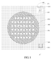
- FIG. 1 is a top plan view of an MEMS microphone in an embodiment
- FIG. 2 is a side cross-sectional view taken along line A-A' of FIG. 1 .
- An MEMS microphone includes a substrate 110, a lower electrode layer 120, a sacrificial layer 130, a stress layer 140, and an upper electrode layer 150.
- the substrate 110 is made of Si, and the substrate 110 may also be made of other semiconductors or semiconductor compounds, such as one of Ge, SiGe, SiC, SiO 2 , or Si 3 N 4 .
- the middle portion of the base plate 110 is provided with a first opening 111.
- the first opening 111 is also called a back cavity.
- the substrate 110 may also be provided with an insulating layer 113.
- the insulating layer 113 is a silicon oxide layer.
- the insulating layer 113 serves as a stop layer for etching the back cavity 111 at the same time.
- the lower electrode layer 120 spans and is connected to the insulating layer 113.
- the insulating layer 113 serves to insulate the substrate 110 and the lower electrode layer 120 from each other.
- the lower electrode layer 120 spans the substrate 110.
- the sacrificial layer 130, the stress layer 140, and the upper electrode layer 150 are sequentially laminated on the lower electrode layer 120.
- a second opening 160 is defined on the sacrificial layer 130 and the stress layer 140.
- the second opening 160 is corresponding to the first opening 111.
- the stress direction of the stress layer 140 is opposite to the warp direction of the substrate 110.
- the direction of the arrow A in FIG 2 indicates the direction of the force of the stress layer 140
- the direction of the arrow B in FIG. 2 indicates the direction of the force of the film layer that causes warping of the wafer, that is, the direction of the force of the warpage of the substrate 110.
- the thickness of the stress layer 140 matches the warpage of the substrate 110.
- the warpage or warp is used to describe the degree of bending of the plane in space and is numerically defined as the distance between the furthest two points of the warping plane in the height direction.
- the warpage of the absolute plane is 0.
- the upper electrode layer 150 and the lower electrode layer 120 are insulated from each other.
- the warpage of the substrate 110 can be reduced or eliminated.
- the stress ⁇ of the stress layer 140 multiplied by the thickness t can roughly indicate the magnitude of the force generated by the stress layer 140 on the wafer, which is represented with ⁇ ⁇ t.
- the stress of other layers can also be roughly calculated accordingly. Adjusting the stress and thickness of the stress layer 140 can reduce or eliminate the warpage of the substrate 110.
- the lower electrode layer 120 is a flexible film serving as a diaphragm
- the upper electrode layer 150 is a rigid film serving as a back plate.
- the lower electrode layer (diaphragm) 120 is a flexible film that has tensile stress and is conductive. When the ambient air is vibrated, the diaphragm can deform to a certain degree, so as to form a flat plate capacitor together with the upper electrode layer (back plate) 150, as an electrode of the plate capacitor.
- the upper electrode layer (back plate) 150 is a conductive, rigid film, and a plurality of acoustic holes 170 with specific size are formed on the upper electrode layer (back plate) 150.
- the sound can be conducted through the acoustic holes 170 to the lower electrode layer (diaphragm) 120.
- the acoustic holes 170 are uniformly distributed on the upper electrode layer (back plate) 150.
- the acoustic holes 170 may also be non-uniformly distributed.
- the acoustic holes 170 may be relatively dense in the middle region of the upper electrode layer (back plate) 150.
- the lower electrode layer 120 and the upper electrode layer 150 are both conductive layers.
- the lower electrode layer 120 and the upper electrode layer 150 are both poly silicon layers.
- the process parameters of the polysilicon deposition, the thickness thereof, the doping amount of impurities, and the like can be changed to form the lower electrode layer 120 and the upper electrode layer 150 that are flexible or rigid.
- the electrode plate 120 and the upper electrode layer 150 may also be a composite layer structure including a conductive layer, for example, containing Si, Ge, SiGe, SiC, or Al, W, Ti, or one of the nitrides of Al, W, Ti.
- the lower electrode layer 120 is a rigid film serving as a back plate
- the upper electrode layer 150 is a flexible film serving as a diaphragm.
- a plurality of acoustic holes 170 with specific size are formed on the lower electrode layer 120. The sound can be conducted through the acoustic holes 170 to the upper electrode layer (diaphragm) 150.
- the acoustic holes 170 are uniformly distributed on the lower electrode layer (back plate) 120.
- the acoustic holes 170 may also be non-uniformly distributed.
- the acoustic holes 170 may be relatively dense in the middle region of the lower electrode layer 120.
- the sacrificial layer 130, the stress layer 140, and the upper electrode layer 150 are sequentially laminated on the lower electrode layer 120.
- the second opening 160 is defined on the sacrificial layer 130 and the stress layer 140, so that the lower electrode layer 120, the sacrificial layer 130, the stress layer 140, and the upper electrode layer 150 are enclosed to form a cavity.
- the cavity is actually released from the sacrificial layer 130. During the release, the sacrificial layer 130 is etched away to form a cavity.
- the sacrificial layer 130 with such a thickness may cause severe deformation of the MEMS microphone semiconductor substrate 110.
- the stress magnitude of the stress layer 140 or the film thickness of the stress layer 140 may be controlled according to the actual degree of warping or deformation of the substrate 110, such that the thickness of the stress layer 140 matches the warpage of the substrate 110. In other words, by changing the thickness and stress value of the stress layer 140, a force opposite to the direction of deformation of the substrate 110 may be applied to the substrate 110, so as to reduce or eliminate the deformation of the substrate 110.
- the stress layer 140 is a silicon nitride (Si 3 N 4 ) layer, because the stress direction of the silicon nitride (Si 3 N 4 ) layer is opposite to the stress that causes the substrate 110 to warp.
- the stress layer 140 is typically located at the periphery of a vibration active area of the upper electrode layer 150 or the lower electrode layer 120, so as not to affect the stress level of the diaphragm or the back plate.
- the vibration active area of the upper electrode layer 150 or the lower electrode layer 120 refers to a position corresponding to the second opening 160.
- the sacrificial layer 130 is a poly silicon layer, and the sacrificial layer 130 is provided with a notch 131 for exposing the lower electrode layer 120 below the sacrificial layer 130.
- the notch 131 is a through hole structure.
- the MEMS microphone also includes a first pad 181 disposed on a side of the upper electrode layer 150, and a second pad 183 disposed on the exposed lower electrode 120.
- the first pad 181 and the second pad 183 are both made of metal, and the first pad 181 and the second pad 183 are used to connect the lower electrode layer 120 and the upper electrode layer 150, meanwhile, the first pad 181 and the second pad 183 can also be used for subsequent capacitive silica-based microphone packaging wiring.
- FIGs. 1 to 4 only illustrate simple examples of some major structures of the MEMS microphone and do not represent the entire structure of the device.
- FIG. 4 is a flowchart of a method of manufacturing the MEMS microphone. A specific process flow will be described below with reference to FIGs. 5 to 12 .
- the foregoing method of manufacturing the MEMS microphone includes: In step S410, a lower electrode layer, a sacrificial layer, and a stress layer are sequentially deposited on the substrate.
- the substrate 110 is made of Si. In other embodiments, the substrate 110 may also be made of other semiconductors or semiconductor compounds, such as one of Ge, SiGe, SiC, SiO 2 , or Si 3 N 4 .
- a silicon oxide insulating layer 113 is formed on the surface (first main surface) of the substrate 110 by thermal growth, and the thickness of the silicon oxide insulating layer 113 is between 0.5 ⁇ m and 1 ⁇ m.
- the polysilicon is deposited on the surface of the silicon oxide insulating layer 113 to form the lower electrode layer 120.
- the lower electrode layer 120 is a flexible film and the lower electrode layer 120 serves as a diaphragm of the MEMS microphone.
- the lower electrode layer 120 may also be a composite conductive layer containing Si, Ge, SiGe, SiC, or Al, W, Ti, or nitrides of Al, W, Ti.
- the photolithography and etching steps are then followed to form the desired pattern of the lower electrode layer (diaphragm) 120; an oxide layer is then deposited over the lower electrode layer 120 serving as a sacrificial layer 130; and a layer of nitride is deposited over the sacrificial layer 130 to serve as the stress layer 140.
- the thickness of the sacrificial layer of the MEMS microphone is usually in the range of 3 to 5 ⁇ m, sacrificial layer 130 with such a thickness will cause severe deformation of the MEMS microphone semiconductor substrate 110.
- the press of the stress layer 140 or the film thickness of the stress layer 140 can be controlled according to the warpage or the deformation of the substrate 110.
- the stress layer 140 is a silicon nitride (Si 3 N 4 ) layer, and the stress direction of the silicon nitride (Si 3 N 4 ) layer is opposite to the stress that causes the substrate 110 to warp.
- the stress of the stress layer 140 may be adjusted by adjusting deposition process parameters such as temperature, pressure, gas volume (total reaction gas volume and ratio of reactant gas components), radio frequency power and frequency, and the like in depositing.
- step S420 a vibration active region of the lower electrode layer is formed in the stress layer.
- the vibration active region 141 of the lower electrode layer (diaphragm) 120 is formed on the stress layer 140, and the first through hole 143 is formed by etching.
- the vibration active region can be interpreted as a space to allow the lower electrode layer 120 serving as a diaphragm in the MEMS microphone to be deformed to a certain degree when the surrounding air vibrates.
- step S430 an upper electrode layer is deposited on the stress layer.
- polysilicon is deposited on the stress adjustment layer 140 to form a rigid film having conductive properties, that is, the upper electrode layer 150 serves as a back plate of the MEMS microphone.
- Photolithography and etching are performed on the upper electrode layer 150 to form the acoustic holes 170 and the second through hole 151.
- the acoustic holes 170 are uniformly distributed on the upper electrode layer 150.
- the acoustic holes 170 may also be non-uniformly distributed.
- the acoustic holes 170 may be relatively dense in the middle region of the upper electrode layer 150.
- the stress layer 140 is typically located at the periphery of the vibration active area of the upper electrode layer 150 or the lower electrode layer 120 so as not to affect the stress level of the diaphragm or the back plate.
- a first pad 181 is formed on a side of the upper electrode layer (back plate) 150, and a second pad 183 is formed on a lower electrode layer (diaphragm) 120 corresponding to the third through hole.
- the first pad 181 and the second pad 183 are used to connect the lower electrode layer (diaphragm) 120 and the upper electrode layer (back plate) 150, and the first pad 181 and the second pad 183 may also be used for subsequent capacitive silica-based microphone packaging wiring.
- step S440 a first opening is defined on the substrate.
- the surface of the substrate 110 facing away from the lower electrode layer 120 (the second main surface) is ground to reduce the thickness of the substrate 110 to a desired thickness; and a first opening 111 is defined on the second main surface by a process such as photolithography and etching.
- the first opening 111 is also referred to as the back cavity.
- the insulating layer 113 serves as a stop layer for etching the back cavity 111.
- step S450 a second opening is defined on the sacrificial layer corresponding to the vibration active area.
- the sacrificial layer corresponding to the vibration active area undergoes a release process to define a second opening 160 so that the lower electrode layer 120, the sacrificial layer 130, the stress layer 140, and the upper electrode layer 150 are enclosed to form a cavity.
- the release means that the sacrificial layer 130 is etched away in a specific region (position corresponding to the vibration active region of the lower electrode layer or the lower motor layer of the diaphragm) by an etching process, and an MEMS microphone device is finally formed.
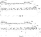
- the preparation process flow of the MEMS microphone is as follows, which will be described with reference to FIGs. 13 to 18 .
- step S410 a lower electrode layer, a sacrificial layer, and a stress layer are sequentially deposited on the substrate.
- a substrate 110 is provided.
- the substrate 110 is made of Si.
- the substrate 110 may also be made of other semiconductors or semiconductor compounds, such as one of Ge, SiGe, SiC, SiO 2 or Si 3 N 4 .
- a silicon oxide insulating layer 113 is formed on the surface (first main surface) of the substrate 110 by thermal growth, and the thickness of the silicon oxide insulating layer 113 is between 0.5 ⁇ m and 1 ⁇ m.
- Poly silicon is then deposited on the surface of the silicon oxide insulating layer 113 to form the lower electrode layer 120.
- polysilicon is deposited on the surface of the silicon oxide insulating layer 113 to form the lower electrode layer 120.
- the lower electrode layer 120 is a rigid film and the lower electrode layer 120 serves as a back plate of the MEMS microphone.
- the lower electrode layer 120 may also be a composite conductive layer containing Si, Ge, SiGe, SiC, or Al, W, Ti, or nitrides of Al, W, Ti.
- acoustic holes 170 are evenly distributed on the lower electrode layer 120.
- the acoustic holes 170 may also be non-uniformly distributed.
- the acoustic holes 170 may be relatively dense in the middle region of the lower electrode layer 120.
- An oxide layer is then deposited on the lower electrode layer 120 serving as a sacrificial layer 130, and a layer of silicon nitride is deposited serving as a stress layer 140 on the sacrificial layer 130.
- the sacrificial layer 130 with such a thickness will cause severe deformation of the MEMS microphone semiconductor substrate 110.
- the press of the stress layer 140 or the film thickness of the stress layer 140 can be controlled according to the warpage or the deformation of the substrate 110. In other words, by changing the thickness and the stress of the stress layer 140, a force opposite to the direction of the deformation of the substrate may be applied to the substrate so as to reduce or eliminate the deformation of the substrate.
- the stress layer 140 is a silicon nitride (Si 3 N 4 ) layer, and the stress direction of the silicon nitride (Si 3 N 4 ) layer is opposite to the stress that causes the substrate 110 to warp.
- the stress of the stress layer 140 may be adjusted by adjusting deposition process parameters such as temperature, pressure, gas volume (total reaction gas volume and ratio of reactant gas components), radio frequency power and frequency, and the like in depositing.
- step S420 A vibration active region of the upper electrode layer is formed in the stress layer.
- a vibration active region 141 of the upper electrode layer (diaphragm) 150 is formed on the stress layer 140, and the first through hole 143 is formed by etching.
- the vibration active region can be understood to mean that the upper electrode layer 150 serving as a diaphragm in the MEMS microphone has a space that can deform to a certain degree when the surrounding air vibrates.
- step S430 an upper electrode layer is deposited on the stress layer.
- poly silicon is deposited on the stress layer 140 to form a flexible thin film having conductive properties, that is, the upper electrode layer 150, which serves as a diaphragm of the MEMS microphone.
- the stress layer 140 is typically located at the periphery of the vibration active area of the upper electrode layer 150 or the lower electrode layer 120 so as not to affect the stress level of the diaphragm or the back plate.
- photolithography, etching, and other processes are performed to form the desired pattern and the second through hole 151.
- a third through hole 131 is formed in the second through hole 151 on the sacrificial layer 130 through a photolithography and etching process.
- a first pad 181 is formed on a side of the upper electrode layer (diaphragm) 150, and a second pad 183 is formed on a lower electrode layer (back plate) 120 corresponding to the third through hole.
- the first pad 181 and the second pad 183 are used to connect the lower electrode layer (diaphragm) 120 and the upper electrode layer (back plate) 150, and the first pad 181 and the second pad 183 may also be used for subsequent capacitive silica-based microphone packaging wiring.
- step S440 a first opening is defined on the substrate.
- the surface of the substrate 110 facing away from the lower electrode layer 120 (the second main surface) is ground to reduce the thickness of the substrate 110 to a desired thickness; and a first opening 111 is defined on the second main surface by a process such as photolithography and etching.
- the first opening 111 is also referred to as back cavity.
- the insulating layer 113 serves as a stop layer for etching the back cavity 111.
- step S450 a second opening is defined on the sacrificial layer corresponding to the vibration active area, and the second opening is corresponding to the first opening.
- the sacrificial layer corresponding to the vibration active area undergoes a release process to define a second opening 160 so that the lower electrode layer 120, the sacrificial layer 130, the stress layer 140, and the upper electrode layer 150 are enclosed to form a cavity.
- the release means that the sacrificial layer 130 is etched away in a specific region (position corresponding to the vibration active region of the lower electrode layer or the lower motor layer of the diaphragm) by an etching process, and an MEMS microphone device is finally formed.
- the substrate 100 represents a support structure that provides support and does not necessarily represent that the substrate 100 is a separate component.
- the substrate 100 may be represented as a multi-layer structure, and its multi-layer structure may be formed by a process such as epitaxy, deposition, or bonding.
- the above MEMS microphone includes a substrate, a lower electrode layer, a sacrificial layer, a stress layer, and an upper electrode layer.
- the stress or thickness of the stress layer matches the warping degree of the substrate, by changing the thickness and the stress value of the stress layer, a force opposite to the deformation direction of the substrate can be applied to the substrate so as to reduce or eliminate the deformation of the substrate.
- the method of manufacturing the MEMS microphone can be perfectly compatible with the existing manufacturing process of MEMS microphones, which facilitates production, does not require the purchase of special requirements substrates, and has a low cost. At the same time, it can effectively reduce the risk of scratches and contamination on the front surface of the MEMS microphone substrate, and the product yield is high.
Landscapes
- Engineering & Computer Science (AREA)
- Physics & Mathematics (AREA)
- Acoustics & Sound (AREA)
- Signal Processing (AREA)
- Manufacturing & Machinery (AREA)
- Microelectronics & Electronic Packaging (AREA)
- Computer Hardware Design (AREA)
- Multimedia (AREA)
- Electrostatic, Electromagnetic, Magneto- Strictive, And Variable-Resistance Transducers (AREA)
- Micromachines (AREA)
- Pressure Sensors (AREA)
Abstract
Description
- The present disclosure relates to semiconductor device technology, and particularly relates to an MEMS microphone and a method of manufacturing the same.
- A Micro-Electro-Mechanical System (MEMS) device, including a silica-based microphone, is usually manufactured by way of integrated circuit manufacturing technology. Silica-based microphones have broad application prospects in areas such as hearing aids and mobile communication devices. MEMS microphone chips have been researched for more than 20 years. During this period, many types of microphone chips have been developed, including piezoresistive, piezoelectric, and capacitive, among which capacitive MEMS microphones are the most widely used. Capacitive MEMS microphones have the following advantages: small size, high sensitivity, favorable frequency characteristics, and low noise and so on.
- In the manufacturing process of MEMS microphones, the process is usually performed only on one side of the semiconductor substrate (e.g., film deposition, etching, etc.) while on the other side the process is not performed. Usually, a very thick layer of silicon oxide is formed on the diaphragm or the back plate serving as a sacrificial layer, typically with a thickness of 3 to 5 µm. Then a back plate or a diaphragm is formed on the sacrificial layer, and finally the sacrificial layer is etched away to form a cavity between the back plate and the diaphragm. This very thick sacrificial layer can cause severe distortion of the MEMS microphone semiconductor substrate. As there are strict requirements on the deformation of the semiconductor substrate in the semiconductor manufacturing process, such as a photolithography process, if the semiconductor substrate is severely deformed, subsequent processes cannot be performed, resulting that the MEMS microphone production cannot carry on.
- In order to address the warpage problem of the semiconductor substrate, typically a film layer is also deposited on the other side of the semiconductor substrate or an etching process is performed. However, this may cause one side of the semiconductor substrate of the MEMS microphone device to be in contact with the semiconductor device, such that the MEMS microphone device is scratched or contaminated, whereby the yield of the MEMS microphone is affected and the manufacturing cost is also increased. Additionally, due to limitations in the production process, the backside film layer cannot always be maintained on the backside of the semiconductor substrate. Once the film on the back side is removed, the semiconductor substrate will be deformed again.
- Accordingly, it is necessary to provide an MEMS microphone and a manufacturing method thereof that can decrease or eliminate the deformation of the substrate and have a high yield.
- An MEMS microphone includes a substrate, a lower electrode layer, a sacrificial layer, a stress layer, and an upper electrode layer; the substrate defines a first opening in a middle portion thereof, the lower electrode layer spans the substrate; the sacrificial layer, the stress layer, and the upper electrode layer are sequentially laminated on the lower electrode layer; the sacrificial layer and the stress layer define a second opening corresponding to the first opening; a stress direction of the stress layer is opposite to a warping direction of the substrate.
- Additionally, a method of manufacturing an MEMS microphone is also provided, which includes:
- depositing a lower electrode layer, a sacrificial layer, and a stress layer sequentially on a substrate, wherein a stress direction of the stress layer is opposite to a warp direction of the substrate;
- forming a vibration active region of an upper electrode layer on the stress layer;
- depositing an upper electrode layer on the stress layer;
- defining a first opening on the substrate; and
- defining a second opening on the sacrificial layer corresponding to the vibration active area, wherein the second opening corresponds to the first opening.
- Additionally, a method of manufacturing an MEMS microphone is also provided, which includes:
- depositing a lower electrode layer, a sacrificial layer, and a stress layer sequentially on a substrate, wherein a stress direction of the stress layer is opposite to a warp direction of the substrate;
- forming a vibration active region of the lower electrode layer on the stress layer;
- depositing an upper electrode layer on the stress layer;
- defining a first opening on the substrate; and
- defining a second opening on the sacrificial layer corresponding to the vibration active area, wherein the second opening is corresponding to the first opening.
- The above MEMS microphone includes a substrate, a lower electrode layer, a sacrificial layer, a stress layer, and an upper electrode layer.
- To illustrate the technical solutions according to the embodiments of the present disclosure or in the prior art more clearly, the accompanying drawings for describing the embodiments or the prior art are introduced briefly in the following. Apparently, the accompanying drawings in the following description are only some embodiments of the present disclosure, and persons of ordinary skill in the art can derive other drawings from the accompanying drawings without creative efforts.
-
FIG. 1 is a top plan view of an MEMS microphone in an embodiment; -
FIG. 2 is a cross-sectional view taken along line A-A' ofFIG. 1 ; -
FIG. 3 is a cross-sectional view of an MEMS microphone in another embodiment; -
FIG. 4 is a flowchart of a method of manufacturing the MEMS microphone in an embodiment; -
FIGs. 5-12 are cross-sectional views illustrating the manufacturing process of the MEMS microphone in an embodiment; and -
FIGs. 13-18 are cross-sectional views illustrating the manufacturing process of the MEMS microphone in another embodiment. - Embodiments of the disclosure are described more comprehensively hereinafter with reference to the accompanying drawings. Preferable embodiments are presented in the drawings. The various embodiments of the disclosure may, however, be embodied in many different forms and should not be construed as limited to the embodiments set forth herein. Rather, these embodiments are provided so that this disclosure will be thorough and complete, and will fully convey the scope of the disclosure to those skilled in the art.
-
FIG. 1 is a top plan view of an MEMS microphone in an embodiment;FIG. 2 is a side cross-sectional view taken along line A-A' ofFIG. 1 . - An MEMS microphone includes a
substrate 110, alower electrode layer 120, asacrificial layer 130, astress layer 140, and anupper electrode layer 150. - In the illustrated embodiment, the
substrate 110 is made of Si, and thesubstrate 110 may also be made of other semiconductors or semiconductor compounds, such as one of Ge, SiGe, SiC, SiO2, or Si3N4. The middle portion of thebase plate 110 is provided with afirst opening 111. Thefirst opening 111 is also called a back cavity. Thesubstrate 110 may also be provided with aninsulating layer 113. Theinsulating layer 113 is a silicon oxide layer. The insulatinglayer 113 serves as a stop layer for etching theback cavity 111 at the same time. Thelower electrode layer 120 spans and is connected to theinsulating layer 113. Theinsulating layer 113 serves to insulate thesubstrate 110 and thelower electrode layer 120 from each other. - The
lower electrode layer 120 spans thesubstrate 110. Thesacrificial layer 130, thestress layer 140, and theupper electrode layer 150 are sequentially laminated on thelower electrode layer 120. Asecond opening 160 is defined on thesacrificial layer 130 and thestress layer 140. Thesecond opening 160 is corresponding to thefirst opening 111. Here, the stress direction of thestress layer 140 is opposite to the warp direction of thesubstrate 110. The direction of the arrow A inFIG 2 indicates the direction of the force of thestress layer 140, and the direction of the arrow B inFIG. 2 indicates the direction of the force of the film layer that causes warping of the wafer, that is, the direction of the force of the warpage of thesubstrate 110. - The thickness of the
stress layer 140 matches the warpage of thesubstrate 110. The warpage or warp is used to describe the degree of bending of the plane in space and is numerically defined as the distance between the furthest two points of the warping plane in the height direction. The warpage of the absolute plane is 0. Theupper electrode layer 150 and thelower electrode layer 120 are insulated from each other. - Upon matching of the
stress layer 140 with the stress of the film layer (substrate 110) which causes the warpage of the substrate, the warpage of thesubstrate 110 can be reduced or eliminated. The stress σ of thestress layer 140 multiplied by the thickness t can roughly indicate the magnitude of the force generated by thestress layer 140 on the wafer, which is represented with σ × t. The stress of other layers can also be roughly calculated accordingly. Adjusting the stress and thickness of thestress layer 140 can reduce or eliminate the warpage of thesubstrate 110. - Referring to
FIGs. 1 and2 , thelower electrode layer 120 is a flexible film serving as a diaphragm, theupper electrode layer 150 is a rigid film serving as a back plate. The lower electrode layer (diaphragm) 120 is a flexible film that has tensile stress and is conductive. When the ambient air is vibrated, the diaphragm can deform to a certain degree, so as to form a flat plate capacitor together with the upper electrode layer (back plate) 150, as an electrode of the plate capacitor. The upper electrode layer (back plate) 150 is a conductive, rigid film, and a plurality ofacoustic holes 170 with specific size are formed on the upper electrode layer (back plate) 150. The sound can be conducted through theacoustic holes 170 to the lower electrode layer (diaphragm) 120. Theacoustic holes 170 are uniformly distributed on the upper electrode layer (back plate) 150. Of course, theacoustic holes 170 may also be non-uniformly distributed. For example, theacoustic holes 170 may be relatively dense in the middle region of the upper electrode layer (back plate) 150. - The
lower electrode layer 120 and theupper electrode layer 150 are both conductive layers. In the illustrated embodiment, thelower electrode layer 120 and theupper electrode layer 150 are both poly silicon layers. During depositing polysilicon and forming the polysilicon layer, the process parameters of the polysilicon deposition, the thickness thereof, the doping amount of impurities, and the like can be changed to form thelower electrode layer 120 and theupper electrode layer 150 that are flexible or rigid. In other embodiments, theelectrode plate 120 and theupper electrode layer 150 may also be a composite layer structure including a conductive layer, for example, containing Si, Ge, SiGe, SiC, or Al, W, Ti, or one of the nitrides of Al, W, Ti. - In another embodiment, referring to
FIG. 3 , thelower electrode layer 120 is a rigid film serving as a back plate, theupper electrode layer 150 is a flexible film serving as a diaphragm. Correspondingly, a plurality ofacoustic holes 170 with specific size are formed on thelower electrode layer 120. The sound can be conducted through theacoustic holes 170 to the upper electrode layer (diaphragm) 150. Theacoustic holes 170 are uniformly distributed on the lower electrode layer (back plate) 120. Of course, theacoustic holes 170 may also be non-uniformly distributed. For example, theacoustic holes 170 may be relatively dense in the middle region of thelower electrode layer 120. - The
sacrificial layer 130, thestress layer 140, and theupper electrode layer 150 are sequentially laminated on thelower electrode layer 120. Thesecond opening 160 is defined on thesacrificial layer 130 and thestress layer 140, so that thelower electrode layer 120, thesacrificial layer 130, thestress layer 140, and theupper electrode layer 150 are enclosed to form a cavity. The cavity is actually released from thesacrificial layer 130. During the release, thesacrificial layer 130 is etched away to form a cavity. - Since the thickness of the sacrificial layer of the MEMS microphone is usually in the range of 3 to 5 µm, the
sacrificial layer 130 with such a thickness may cause severe deformation of the MEMSmicrophone semiconductor substrate 110. The stress magnitude of thestress layer 140 or the film thickness of thestress layer 140 may be controlled according to the actual degree of warping or deformation of thesubstrate 110, such that the thickness of thestress layer 140 matches the warpage of thesubstrate 110. In other words, by changing the thickness and stress value of thestress layer 140, a force opposite to the direction of deformation of thesubstrate 110 may be applied to thesubstrate 110, so as to reduce or eliminate the deformation of thesubstrate 110. In the illustrated embodiment, thestress layer 140 is a silicon nitride (Si3N4) layer, because the stress direction of the silicon nitride (Si3N4) layer is opposite to the stress that causes thesubstrate 110 to warp. - The
stress layer 140 is typically located at the periphery of a vibration active area of theupper electrode layer 150 or thelower electrode layer 120, so as not to affect the stress level of the diaphragm or the back plate. The vibration active area of theupper electrode layer 150 or thelower electrode layer 120 refers to a position corresponding to thesecond opening 160. - The
sacrificial layer 130 is a poly silicon layer, and thesacrificial layer 130 is provided with anotch 131 for exposing thelower electrode layer 120 below thesacrificial layer 130. In this embodiment, thenotch 131 is a through hole structure. - The MEMS microphone also includes a
first pad 181 disposed on a side of theupper electrode layer 150, and asecond pad 183 disposed on the exposedlower electrode 120. Thefirst pad 181 and thesecond pad 183 are both made of metal, and thefirst pad 181 and thesecond pad 183 are used to connect thelower electrode layer 120 and theupper electrode layer 150, meanwhile, thefirst pad 181 and thesecond pad 183 can also be used for subsequent capacitive silica-based microphone packaging wiring. It should be understood that,FIGs. 1 to 4 only illustrate simple examples of some major structures of the MEMS microphone and do not represent the entire structure of the device. -
FIG. 4 is a flowchart of a method of manufacturing the MEMS microphone. A specific process flow will be described below with reference toFIGs. 5 to 12 . The foregoing method of manufacturing the MEMS microphone includes:
In step S410, a lower electrode layer, a sacrificial layer, and a stress layer are sequentially deposited on the substrate. - Referring to
FIGs. 5 to FIG. 7 , in the illustrated embodiment, thesubstrate 110 is made of Si. In other embodiments, thesubstrate 110 may also be made of other semiconductors or semiconductor compounds, such as one of Ge, SiGe, SiC, SiO2, or Si3N4. A siliconoxide insulating layer 113 is formed on the surface (first main surface) of thesubstrate 110 by thermal growth, and the thickness of the siliconoxide insulating layer 113 is between 0.5 µm and 1 µm. Next, the polysilicon is deposited on the surface of the siliconoxide insulating layer 113 to form thelower electrode layer 120. At this time, thelower electrode layer 120 is a flexible film and thelower electrode layer 120 serves as a diaphragm of the MEMS microphone. In other embodiments, thelower electrode layer 120 may also be a composite conductive layer containing Si, Ge, SiGe, SiC, or Al, W, Ti, or nitrides of Al, W, Ti. - The photolithography and etching steps are then followed to form the desired pattern of the lower electrode layer (diaphragm) 120; an oxide layer is then deposited over the
lower electrode layer 120 serving as asacrificial layer 130; and a layer of nitride is deposited over thesacrificial layer 130 to serve as thestress layer 140. Since the thickness of the sacrificial layer of the MEMS microphone is usually in the range of 3 to 5 µm,sacrificial layer 130 with such a thickness will cause severe deformation of the MEMSmicrophone semiconductor substrate 110. In the process of preparation, the press of thestress layer 140 or the film thickness of thestress layer 140 can be controlled according to the warpage or the deformation of thesubstrate 110. In other words, by changing the thickness and the stress of thestress layer 140, a force opposite to the direction of the deformation of the substrate may be applied to the substrate so as to reduce or eliminate the deformation of the substrate. Thestress layer 140 is a silicon nitride (Si3N4) layer, and the stress direction of the silicon nitride (Si3N4) layer is opposite to the stress that causes thesubstrate 110 to warp. The stress of thestress layer 140 may be adjusted by adjusting deposition process parameters such as temperature, pressure, gas volume (total reaction gas volume and ratio of reactant gas components), radio frequency power and frequency, and the like in depositing. - In step S420: a vibration active region of the lower electrode layer is formed in the stress layer.
- Referring to
FIG. 8 , through photolithography and etching steps, the vibrationactive region 141 of the lower electrode layer (diaphragm) 120 is formed on thestress layer 140, and the first throughhole 143 is formed by etching. The vibration active region can be interpreted as a space to allow thelower electrode layer 120 serving as a diaphragm in the MEMS microphone to be deformed to a certain degree when the surrounding air vibrates. - In step S430, an upper electrode layer is deposited on the stress layer.
- Referring to
FIGs. 9 to 11 , polysilicon is deposited on thestress adjustment layer 140 to form a rigid film having conductive properties, that is, theupper electrode layer 150 serves as a back plate of the MEMS microphone. - Photolithography and etching are performed on the
upper electrode layer 150 to form theacoustic holes 170 and the second throughhole 151. Theacoustic holes 170 are uniformly distributed on theupper electrode layer 150. Of course, theacoustic holes 170 may also be non-uniformly distributed. For example, theacoustic holes 170 may be relatively dense in the middle region of theupper electrode layer 150. Thestress layer 140 is typically located at the periphery of the vibration active area of theupper electrode layer 150 or thelower electrode layer 120 so as not to affect the stress level of the diaphragm or the back plate. - Still, photolithography and etching are performed on the
upper electrode layer 150, and a third throughhole 131 is formed on thesacrificial layer 130 corresponding to the second through hole. Afirst pad 181 is formed on a side of the upper electrode layer (back plate) 150, and asecond pad 183 is formed on a lower electrode layer (diaphragm) 120 corresponding to the third through hole. Thefirst pad 181 and thesecond pad 183 are used to connect the lower electrode layer (diaphragm) 120 and the upper electrode layer (back plate) 150, and thefirst pad 181 and thesecond pad 183 may also be used for subsequent capacitive silica-based microphone packaging wiring. - In step S440: a first opening is defined on the substrate.
- Referring to
FIG. 12 , the surface of thesubstrate 110 facing away from the lower electrode layer 120 (the second main surface) is ground to reduce the thickness of thesubstrate 110 to a desired thickness; and afirst opening 111 is defined on the second main surface by a process such as photolithography and etching. Thefirst opening 111 is also referred to as the back cavity. The insulatinglayer 113 serves as a stop layer for etching theback cavity 111. - In step S450: a second opening is defined on the sacrificial layer corresponding to the vibration active area.
- Referring to
FIG. 2 , the sacrificial layer corresponding to the vibration active area undergoes a release process to define asecond opening 160 so that thelower electrode layer 120, thesacrificial layer 130, thestress layer 140, and theupper electrode layer 150 are enclosed to form a cavity. The release means that thesacrificial layer 130 is etched away in a specific region (position corresponding to the vibration active region of the lower electrode layer or the lower motor layer of the diaphragm) by an etching process, and an MEMS microphone device is finally formed. - In another embodiment, the preparation process flow of the MEMS microphone is as follows, which will be described with reference to
FIGs. 13 to 18 . - In step S410, a lower electrode layer, a sacrificial layer, and a stress layer are sequentially deposited on the substrate.
- Referring to
FIG. 13 , asubstrate 110 is provided. Thesubstrate 110 is made of Si. Thesubstrate 110 may also be made of other semiconductors or semiconductor compounds, such as one of Ge, SiGe, SiC, SiO2 or Si3N4. A siliconoxide insulating layer 113 is formed on the surface (first main surface) of thesubstrate 110 by thermal growth, and the thickness of the siliconoxide insulating layer 113 is between 0.5 µm and 1 µm. Poly silicon is then deposited on the surface of the siliconoxide insulating layer 113 to form thelower electrode layer 120. Next, polysilicon is deposited on the surface of the siliconoxide insulating layer 113 to form thelower electrode layer 120. At this time, thelower electrode layer 120 is a rigid film and thelower electrode layer 120 serves as a back plate of the MEMS microphone. In other embodiments, thelower electrode layer 120 may also be a composite conductive layer containing Si, Ge, SiGe, SiC, or Al, W, Ti, or nitrides of Al, W, Ti. - Referring to
FIGS. 14-15 , photolithography and etching are performed on thelower electrode layer 120 to formacoustic holes 170. Theacoustic holes 170 are evenly distributed on thelower electrode layer 120. Of course, theacoustic holes 170 may also be non-uniformly distributed. For example, theacoustic holes 170 may be relatively dense in the middle region of thelower electrode layer 120. An oxide layer is then deposited on thelower electrode layer 120 serving as asacrificial layer 130, and a layer of silicon nitride is deposited serving as astress layer 140 on thesacrificial layer 130. Since the thickness of the sacrificial layer of the MEMS microphone is usually in the range of 3 to 5 µm, thesacrificial layer 130 with such a thickness will cause severe deformation of the MEMSmicrophone semiconductor substrate 110. In the process of preparation, the press of thestress layer 140 or the film thickness of thestress layer 140 can be controlled according to the warpage or the deformation of thesubstrate 110. In other words, by changing the thickness and the stress of thestress layer 140, a force opposite to the direction of the deformation of the substrate may be applied to the substrate so as to reduce or eliminate the deformation of the substrate. Thestress layer 140 is a silicon nitride (Si3N4) layer, and the stress direction of the silicon nitride (Si3N4) layer is opposite to the stress that causes thesubstrate 110 to warp. The stress of thestress layer 140 may be adjusted by adjusting deposition process parameters such as temperature, pressure, gas volume (total reaction gas volume and ratio of reactant gas components), radio frequency power and frequency, and the like in depositing. - In step S420: A vibration active region of the upper electrode layer is formed in the stress layer.
- Referring to
FIG. 15 , then through photolithography and etching steps, a vibrationactive region 141 of the upper electrode layer (diaphragm) 150 is formed on thestress layer 140, and the first throughhole 143 is formed by etching. The vibration active region can be understood to mean that theupper electrode layer 150 serving as a diaphragm in the MEMS microphone has a space that can deform to a certain degree when the surrounding air vibrates. - In step S430, an upper electrode layer is deposited on the stress layer.
- Referring to
FIG. 16 , poly silicon is deposited on thestress layer 140 to form a flexible thin film having conductive properties, that is, theupper electrode layer 150, which serves as a diaphragm of the MEMS microphone. Thestress layer 140 is typically located at the periphery of the vibration active area of theupper electrode layer 150 or thelower electrode layer 120 so as not to affect the stress level of the diaphragm or the back plate. Then, photolithography, etching, and other processes are performed to form the desired pattern and the second throughhole 151. Then, a third throughhole 131 is formed in the second throughhole 151 on thesacrificial layer 130 through a photolithography and etching process. Referring toFIG 17 , afirst pad 181 is formed on a side of the upper electrode layer (diaphragm) 150, and asecond pad 183 is formed on a lower electrode layer (back plate) 120 corresponding to the third through hole. Thefirst pad 181 and thesecond pad 183 are used to connect the lower electrode layer (diaphragm) 120 and the upper electrode layer (back plate) 150, and thefirst pad 181 and thesecond pad 183 may also be used for subsequent capacitive silica-based microphone packaging wiring. - In step S440: a first opening is defined on the substrate.
- Referring to
FIG. 18 , the surface of thesubstrate 110 facing away from the lower electrode layer 120 (the second main surface) is ground to reduce the thickness of thesubstrate 110 to a desired thickness; and afirst opening 111 is defined on the second main surface by a process such as photolithography and etching. Thefirst opening 111 is also referred to as back cavity. The insulatinglayer 113 serves as a stop layer for etching theback cavity 111. - In step S450, a second opening is defined on the sacrificial layer corresponding to the vibration active area, and the second opening is corresponding to the first opening.
- Referring to
FIG. 3 , the sacrificial layer corresponding to the vibration active area undergoes a release process to define asecond opening 160 so that thelower electrode layer 120, thesacrificial layer 130, thestress layer 140, and theupper electrode layer 150 are enclosed to form a cavity. The release means that thesacrificial layer 130 is etched away in a specific region (position corresponding to the vibration active region of the lower electrode layer or the lower motor layer of the diaphragm) by an etching process, and an MEMS microphone device is finally formed. - Finally, it should be noted that the substrate 100 represents a support structure that provides support and does not necessarily represent that the substrate 100 is a separate component. The substrate 100 may be represented as a multi-layer structure, and its multi-layer structure may be formed by a process such as epitaxy, deposition, or bonding.
- The above MEMS microphone includes a substrate, a lower electrode layer, a sacrificial layer, a stress layer, and an upper electrode layer. The stress or thickness of the stress layer matches the warping degree of the substrate, by changing the thickness and the stress value of the stress layer, a force opposite to the deformation direction of the substrate can be applied to the substrate so as to reduce or eliminate the deformation of the substrate. At the same time, the method of manufacturing the MEMS microphone can be perfectly compatible with the existing manufacturing process of MEMS microphones, which facilitates production, does not require the purchase of special requirements substrates, and has a low cost. At the same time, it can effectively reduce the risk of scratches and contamination on the front surface of the MEMS microphone substrate, and the product yield is high.
- The different technical features of the above embodiments can have various combinations which are not described for the purpose of brevity. Nevertheless, to the extent the combining of the different technical features do not conflict with each other, all such combinations must be regarded as being within the scope of the disclosure.
- The foregoing implementations are merely specific embodiments of the present disclosure, and are not intended to limit the protection scope of the present disclosure. It should be noted that any variation or replacement readily figured out by persons skilled in the art within the technical scope disclosed in the present disclosure shall all fall into the protection scope of the present disclosure. Therefore, the protection scope of the present disclosure shall be subject to the protection scope of the claims.
Claims (19)
- An MEMS microphone, comprising a substrate, a lower electrode layer, a sacrificial layer, a stress layer, and an upper electrode layer; wherein the substrate defines a first opening in a middle portion thereof, the lower electrode layer spans the substrate; the sacrificial layer, the stress layer, and the upper electrode layer are sequentially laminated on the lower electrode layer; the sacrificial layer and the stress layer define a second opening corresponding to the first opening; a stress direction of the stress layer is opposite to a warping direction of the substrate.
- The MEMS microphone according to claim 1, wherein the stress layer is a silicon nitride layer.
- The MEMS microphone according to claim 1, wherein the stress layer is located at a periphery of a vibration active area of the upper electrode layer or the lower electrode layer, and the vibration activity area is a position corresponding to the second opening.
- The MEMS microphone according to claim 1, wherein the upper electrode layer is a flexible film serving as a diaphragm, and the lower electrode layer is a rigid film serving as a back plate.
- The MEMS microphone according to claim 1, wherein the upper electrode layer is a rigid film serving as a back plate, and the lower electrode layer is a flexible film serving as a diaphragm.
- The MEMS microphone according to claim 4 or 5, wherein the back plate is provided with a plurality of acoustic holes.
- The MEMS microphone according to claim 1, wherein both the upper electrode layer and the lower electrode layer are made of polysilicon.
- The MEMS microphone according to claim 1, wherein both the upper electrode layer and the lower electrode layer are composite layers containing polysilicon.
- The MEMS microphone according to 1, wherein the sacrificial layer is further provided with a notch configured to expose the lower electrode layer below the sacrificial layer.
- The MEMS microphone according to claim 9, wherein the MEMS microphone further comprises a first pad and a second pad;
wherein the first pad is disposed on a side of the upper electrode layer, and the second pad is disposed on the exposed lower electrode. - The MEMS microphone according to claim 1, wherein an insulating layer is further provided on the substrate, the lower electrode layer spans and is connected to the insulating layer, such that the substrate and the lower electrode layer are insulated from each other.
- A method of manufacturing an MEMS microphone, comprising:depositing a lower electrode layer, a sacrificial layer, and a stress layer sequentially on a substrate, wherein a stress direction of the stress layer is opposite to a warp direction of the substrate;forming a vibration active region of an upper electrode layer on the stress layer;depositing an upper electrode layer on the stress layer;defining a first opening on the substrate; anddefining a second opening on the sacrificial layer corresponding to the vibration active area, wherein the second opening corresponds to the first opening.
- The method according to claim 12, wherein the upper electrode layer is a flexible film, and the lower electrode layer is a rigid film, the method further comprises forming a plurality of acoustic holes on the lower electrode layer.
- The method according to claim 12, wherein the upper electrode layer is a rigid film, and the lower electrode layer is a flexible film, the method further comprises forming a plurality of acoustic holes on the upper electrode layer.
- The method according to claim 12, further comprising forming a first pad on the upper electrode layer and a second pad on the lower electrode layer.
- A method of manufacturing an MEMS microphone comprising:depositing a lower electrode layer, a sacrificial layer, and a stress layer sequentially on a substrate, wherein a stress direction of the stress layer is opposite to a warp direction of the substrate;forming a vibration active region of the lower electrode layer on the stress layer;depositing an upper electrode layer on the stress layer;defining a first opening on the substrate; anddefining a second opening on the sacrificial layer corresponding to the vibration active area, wherein the second opening is corresponding to the first opening.
- The method according to claim 16, wherein the upper electrode layer is a flexible film, and the lower electrode layer is a rigid film, the method further comprises forming a plurality of acoustic holes on the lower electrode layer.
- The method according to claim 16, wherein the upper electrode layer is a flexible film, and the lower electrode layer is a rigid film, the method further comprises forming a plurality of acoustic holes on the upper electrode layer.
- The method according to claim 16, further comprising forming a first pad on the upper electrode layer and a second pad on the lower electrode layer.
Applications Claiming Priority (2)
| Application Number | Priority Date | Filing Date | Title |
|---|---|---|---|
| CN201610389572.2A CN107465983B (en) | 2016-06-03 | 2016-06-03 | MEMS microphone and preparation method thereof |
| PCT/CN2017/086158 WO2017206813A1 (en) | 2016-06-03 | 2017-05-26 | Mems microphone and preparation method thereof |
Publications (3)
| Publication Number | Publication Date |
|---|---|
| EP3468226A1 true EP3468226A1 (en) | 2019-04-10 |
| EP3468226A4 EP3468226A4 (en) | 2020-01-22 |
| EP3468226B1 EP3468226B1 (en) | 2021-06-23 |
Family
ID=60479659
Family Applications (1)
| Application Number | Title | Priority Date | Filing Date |
|---|---|---|---|
| EP17805758.4A Active EP3468226B1 (en) | 2016-06-03 | 2017-05-26 | Mems microphone and preparation method thereof |
Country Status (6)
| Country | Link |
|---|---|
| US (1) | US10815122B2 (en) |
| EP (1) | EP3468226B1 (en) |
| JP (1) | JP6793208B2 (en) |
| KR (1) | KR102175855B1 (en) |
| CN (1) | CN107465983B (en) |
| WO (1) | WO2017206813A1 (en) |
Families Citing this family (15)
| Publication number | Priority date | Publication date | Assignee | Title |
|---|---|---|---|---|
| WO2020072904A1 (en) * | 2018-10-05 | 2020-04-09 | Knowles Electronics, Llc | Acoustic transducers with a low pressure zone and diaphragms having enhanced compliance |
| DE112019004979B4 (en) | 2018-10-05 | 2025-10-02 | Knowles Electronics, Llc | Method for manufacturing MEMS membranes comprising corrugations |
| US11206494B2 (en) | 2018-10-05 | 2021-12-21 | Knowles Electronics, Llc | Microphone device with ingress protection |
| CN111170268B (en) * | 2018-11-13 | 2023-05-09 | 中芯国际集成电路制造(上海)有限公司 | MEMS device and method of manufacturing the same |
| CN109831729B (en) * | 2019-01-30 | 2021-04-16 | 武汉大学 | Compact high-sensitivity MEMS micro-capacitance type sensor |
| CN109905505B (en) * | 2019-03-20 | 2020-09-04 | Oppo广东移动通信有限公司 | Shell and electronic equipment |
| CN111924794B (en) * | 2019-05-13 | 2024-06-04 | 无锡华润上华科技有限公司 | Micro-electromechanical system device |
| CN110868681B (en) * | 2019-11-29 | 2021-09-14 | 绍兴中芯集成电路制造股份有限公司 | MEMS microphone warpage compensation method and MEMS microphone wafer |
| CN111285326B (en) * | 2020-02-25 | 2023-08-25 | 绍兴中芯集成电路制造股份有限公司 | MEMS device and method of manufacturing the same |
| CN111491244B (en) * | 2020-03-16 | 2021-11-16 | 歌尔微电子有限公司 | MEMS microphone processing method and MEMS microphone |
| CN111246355B (en) * | 2020-03-30 | 2021-05-25 | 中芯集成电路制造(绍兴)有限公司 | MEMS devices and methods of forming MEMS devices |
| CN111741423B (en) * | 2020-08-21 | 2020-11-20 | 中芯集成电路制造(绍兴)有限公司 | Manufacturing method of MEMS microphone |
| CN114697841A (en) * | 2020-12-30 | 2022-07-01 | 无锡华润上华科技有限公司 | MEMS microphone and vibrating diaphragm structure thereof |
| CN114630252A (en) * | 2022-04-14 | 2022-06-14 | 苏州感芯微系统技术有限公司 | MEMS transducer |
| CN116654864A (en) * | 2023-04-27 | 2023-08-29 | 绍兴中芯集成电路制造股份有限公司 | Composite film forming method and semiconductor device meeting design goals |
Family Cites Families (42)
| Publication number | Priority date | Publication date | Assignee | Title |
|---|---|---|---|---|
| TWI243496B (en) * | 2003-12-15 | 2005-11-11 | Canon Kk | Piezoelectric film element, method of manufacturing the same, and liquid discharge head |
| US20070121972A1 (en) * | 2005-09-26 | 2007-05-31 | Yamaha Corporation | Capacitor microphone and diaphragm therefor |
| CN1960581B (en) | 2005-11-03 | 2011-07-13 | 歌尔声学股份有限公司 | Capacitance type silicon microphone |
| DE102006001493B4 (en) | 2006-01-11 | 2007-10-18 | Austriamicrosystems Ag | MEMS sensor and method of manufacture |
| JP4660426B2 (en) * | 2006-05-31 | 2011-03-30 | 三洋電機株式会社 | Sensor device and diaphragm structure |
| JP2008016919A (en) * | 2006-07-03 | 2008-01-24 | Matsushita Electric Ind Co Ltd | Sound sensitive device |
| DE102006051494B4 (en) * | 2006-10-31 | 2009-02-05 | Advanced Micro Devices, Inc., Sunnyvale | A method of forming a semiconductor structure comprising a strained channel field field effect transistor |
| JP2008259061A (en) | 2007-04-06 | 2008-10-23 | Matsushita Electric Works Ltd | Electrostatic transducer |
| GB2453104B (en) * | 2007-09-19 | 2012-04-25 | Wolfson Microelectronics Plc | Mems device and process |
| JPWO2010079574A1 (en) * | 2009-01-09 | 2012-06-21 | パナソニック株式会社 | MEMS device |
| JP5513813B2 (en) * | 2009-08-31 | 2014-06-04 | 新日本無線株式会社 | MEMS microphone and manufacturing method thereof |
| JP5052589B2 (en) * | 2009-12-10 | 2012-10-17 | アオイ電子株式会社 | microphone |
| KR101109095B1 (en) * | 2009-12-29 | 2012-01-31 | 주식회사 비에스이 | MEMS microphone and its manufacturing method |
| JP2012045659A (en) * | 2010-08-26 | 2012-03-08 | Yamaha Corp | Method of manufacturing mems transducer |
| JP6145990B2 (en) * | 2012-10-29 | 2017-06-14 | セイコーエプソン株式会社 | Manufacturing method of microlens array substrate |
| US8921956B2 (en) * | 2013-01-25 | 2014-12-30 | Infineon Technologies Ag | MEMS device having a back plate with elongated protrusions |
| GB2515836B (en) * | 2013-07-05 | 2016-01-20 | Cirrus Logic Int Semiconductor Ltd | MEMS device and process |
| US9728653B2 (en) * | 2013-07-22 | 2017-08-08 | Infineon Technologies Ag | MEMS device |
| CN104332494B (en) | 2013-07-22 | 2018-09-21 | 无锡华润上华科技有限公司 | A kind of igbt and its manufacturing method |
| CN104347401B (en) | 2013-07-29 | 2017-05-10 | 无锡华润上华半导体有限公司 | Manufacturing method of insulated gate bipolar transistor |
| CN104425245B (en) | 2013-08-23 | 2017-11-07 | 无锡华润上华科技有限公司 | Reverse-conducting insulated gate bipolar transistor npn npn manufacture method |
| JP6248532B2 (en) * | 2013-10-17 | 2017-12-20 | セイコーエプソン株式会社 | 3C-SiC epitaxial layer manufacturing method, 3C-SiC epitaxial substrate, and semiconductor device |
| CN104701356B (en) | 2013-12-06 | 2018-01-12 | 无锡华润上华科技有限公司 | Semiconductor devices and preparation method thereof |
| US20150170928A1 (en) * | 2013-12-16 | 2015-06-18 | Sumitomo Electric Industries, Ltd. | Silicon carbide substrate and fabrication method thereof |
| CN104760925B (en) | 2014-01-07 | 2016-05-25 | 无锡华润上华半导体有限公司 | A kind of preparation method of film support beam |
| CN105097776B (en) | 2014-04-29 | 2018-03-16 | 无锡华润上华科技有限公司 | SOI device and its inter-metal medium Rotating fields and manufacture method |
| CN105097795B (en) | 2014-05-04 | 2018-03-16 | 无锡华润上华科技有限公司 | Has the semiconductor devices of esd protection structure |
| CN105092110A (en) | 2014-05-06 | 2015-11-25 | 无锡华润上华半导体有限公司 | Pressure sensor and manufacturing method thereof |
| CN105095537B (en) | 2014-05-08 | 2018-03-23 | 无锡华润上华科技有限公司 | The simulation model of high tension apparatus and the modeling method of simulation model of high-voltage device |
| CN105174203B (en) | 2014-05-28 | 2016-09-28 | 无锡华润上华半导体有限公司 | The manufacture method of sensor based on MEMS |
| CN105223781B (en) | 2014-06-26 | 2017-06-23 | 无锡华润上华科技有限公司 | A kind of stepper aligns monitoring method |
| CN105226101B (en) | 2014-06-30 | 2018-04-10 | 无锡华润上华科技有限公司 | Junction field effect transistor and its manufacture method |
| CN105445529B (en) | 2014-07-28 | 2018-06-15 | 无锡华润上华科技有限公司 | There is the power-fail detection circuit of timing control |
| CN105446404B (en) | 2014-08-19 | 2017-08-08 | 无锡华润上华半导体有限公司 | Low differential voltage linear voltage stabilizer circuit, chip and electronic equipment |
| CN106158957B (en) | 2015-04-10 | 2019-05-17 | 无锡华润上华科技有限公司 | Laterally diffused metal oxide semiconductor field effect transistor and method of making the same |
| CN106158921B (en) | 2015-04-10 | 2019-07-23 | 无锡华润上华科技有限公司 | Lateral Diffused Metal Oxide Semiconductor Field Effect Transistor with RESURF Structure |
| CN106303867B (en) | 2015-05-13 | 2019-02-01 | 无锡华润上华科技有限公司 | MEMS microphone |
| CN104867826A (en) * | 2015-06-04 | 2015-08-26 | 武汉新芯集成电路制造有限公司 | Method for preventing thin film at edge of silicon chip from being peeled off |
| US20170053832A1 (en) * | 2015-08-20 | 2017-02-23 | Beijing Acuti Microsystems Co., Ltd. | Wafer structure and processing method thereof |
| CN106483758B (en) | 2015-09-02 | 2019-08-20 | 无锡华润上华科技有限公司 | Optical proximity effect modification method and system |
| CN106571370B (en) | 2015-10-08 | 2019-12-10 | 无锡华润上华科技有限公司 | Dielectric capacitor based on SOI technology |
| CN106816468B (en) | 2015-11-30 | 2020-07-10 | 无锡华润上华科技有限公司 | Lateral diffusion metal oxide semiconductor field effect transistor with RESURF structure |
-
2016
- 2016-06-03 CN CN201610389572.2A patent/CN107465983B/en active Active
-
2017
- 2017-05-26 WO PCT/CN2017/086158 patent/WO2017206813A1/en not_active Ceased
- 2017-05-26 JP JP2018563101A patent/JP6793208B2/en active Active
- 2017-05-26 KR KR1020187035904A patent/KR102175855B1/en active Active
- 2017-05-26 EP EP17805758.4A patent/EP3468226B1/en active Active
- 2017-05-26 US US16/305,119 patent/US10815122B2/en active Active
Also Published As
| Publication number | Publication date |
|---|---|
| EP3468226B1 (en) | 2021-06-23 |
| JP2019517750A (en) | 2019-06-24 |
| US10815122B2 (en) | 2020-10-27 |
| WO2017206813A1 (en) | 2017-12-07 |
| KR20190007016A (en) | 2019-01-21 |
| US20200010316A1 (en) | 2020-01-09 |
| EP3468226A4 (en) | 2020-01-22 |
| CN107465983A (en) | 2017-12-12 |
| JP6793208B2 (en) | 2020-12-02 |
| KR102175855B1 (en) | 2020-11-09 |
| CN107465983B (en) | 2021-06-04 |
Similar Documents
| Publication | Publication Date | Title |
|---|---|---|
| EP3468226B1 (en) | Mems microphone and preparation method thereof | |
| TWI404671B (en) | Mems device | |
| US9266716B2 (en) | MEMS acoustic transducer with silicon nitride backplate and silicon sacrificial layer | |
| US8796790B2 (en) | Method and structure of monolithetically integrated micromachined microphone using IC foundry-compatiable processes | |
| EP1931173B1 (en) | Condenser microphone having flexure hinge diaphragm and method of manufacturing the same | |
| CN101346014B (en) | Micro electro-mechanical system microphone and preparation method thereof | |
| CN105721997A (en) | MEMS silicon microphone and preparation method for the same | |
| US20110073967A1 (en) | Apparatus and method of forming a mems acoustic transducer with layer transfer processes | |
| KR20090063950A (en) | Micro speaker manufacturing method and micro speaker manufactured by this method | |
| KR20090059756A (en) | Piezoelectric element micro speaker using MEMS and its manufacturing method | |
| WO2014159552A1 (en) | Mems acoustic transducer with silicon nitride backplate and silicon sacrificial layer | |
| CN114697841A (en) | MEMS microphone and vibrating diaphragm structure thereof | |
| US8735948B2 (en) | Semiconductor device | |
| KR101692717B1 (en) | Capacitive mems microphone and method of making the same | |
| KR101657652B1 (en) | Capacitive mems microphone and method of making the same | |
| KR20020016117A (en) | The Fabrication Process For Microphone Using The MEMS | |
| CN111285326A (en) | MEMS device and method of manufacturing the same | |
| JP4944494B2 (en) | Capacitive sensor | |
| WO2010008344A2 (en) | Extended sensor back volume | |
| US20260028220A1 (en) | Mems microphone and method for manufacturing the same | |
| TWI498272B (en) | Microelectromechanical system device and manufacturing method thereof | |
| JP6885828B2 (en) | MEMS device and its manufacturing method | |
| KR101615106B1 (en) | MEMS Microphone and Manufacturing Method of the Same | |
| CN118283511A (en) | MEMS microphone and manufacturing method thereof | |
| CN118828337A (en) | MEMS microphone and method of manufacturing the same |
Legal Events
| Date | Code | Title | Description |
|---|---|---|---|
| STAA | Information on the status of an ep patent application or granted ep patent |
Free format text: STATUS: THE INTERNATIONAL PUBLICATION HAS BEEN MADE |
|
| PUAI | Public reference made under article 153(3) epc to a published international application that has entered the european phase |
Free format text: ORIGINAL CODE: 0009012 |
|
| STAA | Information on the status of an ep patent application or granted ep patent |
Free format text: STATUS: REQUEST FOR EXAMINATION WAS MADE |
|
| 17P | Request for examination filed |
Effective date: 20181127 |
|
| AK | Designated contracting states |
Kind code of ref document: A1 Designated state(s): AL AT BE BG CH CY CZ DE DK EE ES FI FR GB GR HR HU IE IS IT LI LT LU LV MC MK MT NL NO PL PT RO RS SE SI SK SM TR |
|
| AX | Request for extension of the european patent |
Extension state: BA ME |
|
| DAV | Request for validation of the european patent (deleted) | ||
| DAX | Request for extension of the european patent (deleted) | ||
| A4 | Supplementary search report drawn up and despatched |
Effective date: 20191220 |
|
| RIC1 | Information provided on ipc code assigned before grant |
Ipc: H04R 19/00 20060101ALI20191216BHEP Ipc: H04R 19/04 20060101AFI20191216BHEP |
|
| GRAP | Despatch of communication of intention to grant a patent |
Free format text: ORIGINAL CODE: EPIDOSNIGR1 |
|
| STAA | Information on the status of an ep patent application or granted ep patent |
Free format text: STATUS: GRANT OF PATENT IS INTENDED |
|
| INTG | Intention to grant announced |
Effective date: 20210311 |
|
| GRAS | Grant fee paid |
Free format text: ORIGINAL CODE: EPIDOSNIGR3 |
|
| GRAA | (expected) grant |
Free format text: ORIGINAL CODE: 0009210 |
|
| STAA | Information on the status of an ep patent application or granted ep patent |
Free format text: STATUS: THE PATENT HAS BEEN GRANTED |
|
| AK | Designated contracting states |
Kind code of ref document: B1 Designated state(s): AL AT BE BG CH CY CZ DE DK EE ES FI FR GB GR HR HU IE IS IT LI LT LU LV MC MK MT NL NO PL PT RO RS SE SI SK SM TR |
|
| REG | Reference to a national code |
Ref country code: GB Ref legal event code: FG4D |
|
| REG | Reference to a national code |
Ref country code: CH Ref legal event code: EP |
|
| REG | Reference to a national code |
Ref country code: DE Ref legal event code: R096 Ref document number: 602017040911 Country of ref document: DE Ref country code: AT Ref legal event code: REF Ref document number: 1405341 Country of ref document: AT Kind code of ref document: T Effective date: 20210715 |
|
| REG | Reference to a national code |
Ref country code: IE Ref legal event code: FG4D |
|
| REG | Reference to a national code |
Ref country code: NL Ref legal event code: FP |
|
| REG | Reference to a national code |
Ref country code: LT Ref legal event code: MG9D |
|
| PG25 | Lapsed in a contracting state [announced via postgrant information from national office to epo] |
Ref country code: LT Free format text: LAPSE BECAUSE OF FAILURE TO SUBMIT A TRANSLATION OF THE DESCRIPTION OR TO PAY THE FEE WITHIN THE PRESCRIBED TIME-LIMIT Effective date: 20210623 Ref country code: FI Free format text: LAPSE BECAUSE OF FAILURE TO SUBMIT A TRANSLATION OF THE DESCRIPTION OR TO PAY THE FEE WITHIN THE PRESCRIBED TIME-LIMIT Effective date: 20210623 Ref country code: HR Free format text: LAPSE BECAUSE OF FAILURE TO SUBMIT A TRANSLATION OF THE DESCRIPTION OR TO PAY THE FEE WITHIN THE PRESCRIBED TIME-LIMIT Effective date: 20210623 Ref country code: BG Free format text: LAPSE BECAUSE OF FAILURE TO SUBMIT A TRANSLATION OF THE DESCRIPTION OR TO PAY THE FEE WITHIN THE PRESCRIBED TIME-LIMIT Effective date: 20210923 |
|
| REG | Reference to a national code |
Ref country code: AT Ref legal event code: MK05 Ref document number: 1405341 Country of ref document: AT Kind code of ref document: T Effective date: 20210623 |
|
| PG25 | Lapsed in a contracting state [announced via postgrant information from national office to epo] |
Ref country code: GR Free format text: LAPSE BECAUSE OF FAILURE TO SUBMIT A TRANSLATION OF THE DESCRIPTION OR TO PAY THE FEE WITHIN THE PRESCRIBED TIME-LIMIT Effective date: 20210924 Ref country code: NO Free format text: LAPSE BECAUSE OF FAILURE TO SUBMIT A TRANSLATION OF THE DESCRIPTION OR TO PAY THE FEE WITHIN THE PRESCRIBED TIME-LIMIT Effective date: 20210923 Ref country code: LV Free format text: LAPSE BECAUSE OF FAILURE TO SUBMIT A TRANSLATION OF THE DESCRIPTION OR TO PAY THE FEE WITHIN THE PRESCRIBED TIME-LIMIT Effective date: 20210623 Ref country code: RS Free format text: LAPSE BECAUSE OF FAILURE TO SUBMIT A TRANSLATION OF THE DESCRIPTION OR TO PAY THE FEE WITHIN THE PRESCRIBED TIME-LIMIT Effective date: 20210623 Ref country code: SE Free format text: LAPSE BECAUSE OF FAILURE TO SUBMIT A TRANSLATION OF THE DESCRIPTION OR TO PAY THE FEE WITHIN THE PRESCRIBED TIME-LIMIT Effective date: 20210623 |
|
| PG25 | Lapsed in a contracting state [announced via postgrant information from national office to epo] |
Ref country code: ES Free format text: LAPSE BECAUSE OF FAILURE TO SUBMIT A TRANSLATION OF THE DESCRIPTION OR TO PAY THE FEE WITHIN THE PRESCRIBED TIME-LIMIT Effective date: 20210623 Ref country code: SM Free format text: LAPSE BECAUSE OF FAILURE TO SUBMIT A TRANSLATION OF THE DESCRIPTION OR TO PAY THE FEE WITHIN THE PRESCRIBED TIME-LIMIT Effective date: 20210623 Ref country code: SK Free format text: LAPSE BECAUSE OF FAILURE TO SUBMIT A TRANSLATION OF THE DESCRIPTION OR TO PAY THE FEE WITHIN THE PRESCRIBED TIME-LIMIT Effective date: 20210623 Ref country code: RO Free format text: LAPSE BECAUSE OF FAILURE TO SUBMIT A TRANSLATION OF THE DESCRIPTION OR TO PAY THE FEE WITHIN THE PRESCRIBED TIME-LIMIT Effective date: 20210623 Ref country code: PT Free format text: LAPSE BECAUSE OF FAILURE TO SUBMIT A TRANSLATION OF THE DESCRIPTION OR TO PAY THE FEE WITHIN THE PRESCRIBED TIME-LIMIT Effective date: 20211025 Ref country code: AT Free format text: LAPSE BECAUSE OF FAILURE TO SUBMIT A TRANSLATION OF THE DESCRIPTION OR TO PAY THE FEE WITHIN THE PRESCRIBED TIME-LIMIT Effective date: 20210623 Ref country code: EE Free format text: LAPSE BECAUSE OF FAILURE TO SUBMIT A TRANSLATION OF THE DESCRIPTION OR TO PAY THE FEE WITHIN THE PRESCRIBED TIME-LIMIT Effective date: 20210623 Ref country code: CZ Free format text: LAPSE BECAUSE OF FAILURE TO SUBMIT A TRANSLATION OF THE DESCRIPTION OR TO PAY THE FEE WITHIN THE PRESCRIBED TIME-LIMIT Effective date: 20210623 |
|
| PG25 | Lapsed in a contracting state [announced via postgrant information from national office to epo] |
Ref country code: PL Free format text: LAPSE BECAUSE OF FAILURE TO SUBMIT A TRANSLATION OF THE DESCRIPTION OR TO PAY THE FEE WITHIN THE PRESCRIBED TIME-LIMIT Effective date: 20210623 |
|
| REG | Reference to a national code |
Ref country code: DE Ref legal event code: R097 Ref document number: 602017040911 Country of ref document: DE |
|
| PG25 | Lapsed in a contracting state [announced via postgrant information from national office to epo] |
Ref country code: DK Free format text: LAPSE BECAUSE OF FAILURE TO SUBMIT A TRANSLATION OF THE DESCRIPTION OR TO PAY THE FEE WITHIN THE PRESCRIBED TIME-LIMIT Effective date: 20210623 |
|
| PLBE | No opposition filed within time limit |
Free format text: ORIGINAL CODE: 0009261 |
|
| STAA | Information on the status of an ep patent application or granted ep patent |
Free format text: STATUS: NO OPPOSITION FILED WITHIN TIME LIMIT |
|
| 26N | No opposition filed |
Effective date: 20220324 |
|
| PG25 | Lapsed in a contracting state [announced via postgrant information from national office to epo] |
Ref country code: AL Free format text: LAPSE BECAUSE OF FAILURE TO SUBMIT A TRANSLATION OF THE DESCRIPTION OR TO PAY THE FEE WITHIN THE PRESCRIBED TIME-LIMIT Effective date: 20210623 |
|
| PG25 | Lapsed in a contracting state [announced via postgrant information from national office to epo] |
Ref country code: IT Free format text: LAPSE BECAUSE OF FAILURE TO SUBMIT A TRANSLATION OF THE DESCRIPTION OR TO PAY THE FEE WITHIN THE PRESCRIBED TIME-LIMIT Effective date: 20210623 |
|
| REG | Reference to a national code |
Ref country code: CH Ref legal event code: PL |
|
| REG | Reference to a national code |
Ref country code: BE Ref legal event code: MM Effective date: 20220531 |
|
| PG25 | Lapsed in a contracting state [announced via postgrant information from national office to epo] |
Ref country code: MC Free format text: LAPSE BECAUSE OF FAILURE TO SUBMIT A TRANSLATION OF THE DESCRIPTION OR TO PAY THE FEE WITHIN THE PRESCRIBED TIME-LIMIT Effective date: 20210623 Ref country code: LU Free format text: LAPSE BECAUSE OF NON-PAYMENT OF DUE FEES Effective date: 20220526 Ref country code: LI Free format text: LAPSE BECAUSE OF NON-PAYMENT OF DUE FEES Effective date: 20220531 Ref country code: CH Free format text: LAPSE BECAUSE OF NON-PAYMENT OF DUE FEES Effective date: 20220531 |
|
| PG25 | Lapsed in a contracting state [announced via postgrant information from national office to epo] |
Ref country code: IE Free format text: LAPSE BECAUSE OF NON-PAYMENT OF DUE FEES Effective date: 20220526 |
|
| PG25 | Lapsed in a contracting state [announced via postgrant information from national office to epo] |
Ref country code: BE Free format text: LAPSE BECAUSE OF NON-PAYMENT OF DUE FEES Effective date: 20220531 |
|
| PG25 | Lapsed in a contracting state [announced via postgrant information from national office to epo] |
Ref country code: HU Free format text: LAPSE BECAUSE OF FAILURE TO SUBMIT A TRANSLATION OF THE DESCRIPTION OR TO PAY THE FEE WITHIN THE PRESCRIBED TIME-LIMIT; INVALID AB INITIO Effective date: 20170526 |
|
| PG25 | Lapsed in a contracting state [announced via postgrant information from national office to epo] |
Ref country code: MK Free format text: LAPSE BECAUSE OF FAILURE TO SUBMIT A TRANSLATION OF THE DESCRIPTION OR TO PAY THE FEE WITHIN THE PRESCRIBED TIME-LIMIT Effective date: 20210623 Ref country code: CY Free format text: LAPSE BECAUSE OF FAILURE TO SUBMIT A TRANSLATION OF THE DESCRIPTION OR TO PAY THE FEE WITHIN THE PRESCRIBED TIME-LIMIT Effective date: 20210623 |
|
| PG25 | Lapsed in a contracting state [announced via postgrant information from national office to epo] |
Ref country code: MT Free format text: LAPSE BECAUSE OF FAILURE TO SUBMIT A TRANSLATION OF THE DESCRIPTION OR TO PAY THE FEE WITHIN THE PRESCRIBED TIME-LIMIT Effective date: 20210623 |
|
| PGFP | Annual fee paid to national office [announced via postgrant information from national office to epo] |
Ref country code: NL Payment date: 20250314 Year of fee payment: 9 |
|
| PGFP | Annual fee paid to national office [announced via postgrant information from national office to epo] |
Ref country code: FR Payment date: 20250305 Year of fee payment: 9 |
|
| PGFP | Annual fee paid to national office [announced via postgrant information from national office to epo] |
Ref country code: DE Payment date: 20250519 Year of fee payment: 9 |
|
| PG25 | Lapsed in a contracting state [announced via postgrant information from national office to epo] |
Ref country code: TR Free format text: LAPSE BECAUSE OF FAILURE TO SUBMIT A TRANSLATION OF THE DESCRIPTION OR TO PAY THE FEE WITHIN THE PRESCRIBED TIME-LIMIT Effective date: 20210623 |
|
| PGFP | Annual fee paid to national office [announced via postgrant information from national office to epo] |
Ref country code: GB Payment date: 20260323 Year of fee payment: 10 |