EP3467566A1 - Fabry-perot interference filter and production method for fabry-perot interference filter - Google Patents
Fabry-perot interference filter and production method for fabry-perot interference filter Download PDFInfo
- Publication number
- EP3467566A1 EP3467566A1 EP17802546.6A EP17802546A EP3467566A1 EP 3467566 A1 EP3467566 A1 EP 3467566A1 EP 17802546 A EP17802546 A EP 17802546A EP 3467566 A1 EP3467566 A1 EP 3467566A1
- Authority
- EP
- European Patent Office
- Prior art keywords
- outer edge
- layer
- fabry
- laminate
- interference filter
- Prior art date
- Legal status (The legal status is an assumption and is not a legal conclusion. Google has not performed a legal analysis and makes no representation as to the accuracy of the status listed.)
- Pending
Links
Images






Classifications
-
- G—PHYSICS
- G01—MEASURING; TESTING
- G01J—MEASUREMENT OF INTENSITY, VELOCITY, SPECTRAL CONTENT, POLARISATION, PHASE OR PULSE CHARACTERISTICS OF INFRARED, VISIBLE OR ULTRAVIOLET LIGHT; COLORIMETRY; RADIATION PYROMETRY
- G01J3/00—Spectrometry; Spectrophotometry; Monochromators; Measuring colours
- G01J3/12—Generating the spectrum; Monochromators
- G01J3/26—Generating the spectrum; Monochromators using multiple reflection, e.g. Fabry-Perot interferometer, variable interference filters
-
- G—PHYSICS
- G02—OPTICS
- G02B—OPTICAL ELEMENTS, SYSTEMS OR APPARATUS
- G02B26/00—Optical devices or arrangements for the control of light using movable or deformable optical elements
-
- B—PERFORMING OPERATIONS; TRANSPORTING
- B23—MACHINE TOOLS; METAL-WORKING NOT OTHERWISE PROVIDED FOR
- B23K—SOLDERING OR UNSOLDERING; WELDING; CLADDING OR PLATING BY SOLDERING OR WELDING; CUTTING BY APPLYING HEAT LOCALLY, e.g. FLAME CUTTING; WORKING BY LASER BEAM
- B23K26/00—Working by laser beam, e.g. welding, cutting or boring
- B23K26/0006—Working by laser beam, e.g. welding, cutting or boring taking account of the properties of the material involved
-
- B—PERFORMING OPERATIONS; TRANSPORTING
- B23—MACHINE TOOLS; METAL-WORKING NOT OTHERWISE PROVIDED FOR
- B23K—SOLDERING OR UNSOLDERING; WELDING; CLADDING OR PLATING BY SOLDERING OR WELDING; CUTTING BY APPLYING HEAT LOCALLY, e.g. FLAME CUTTING; WORKING BY LASER BEAM
- B23K26/00—Working by laser beam, e.g. welding, cutting or boring
- B23K26/02—Positioning or observing the workpiece, e.g. with respect to the point of impact; Aligning, aiming or focusing the laser beam
- B23K26/06—Shaping the laser beam, e.g. by masks or multi-focusing
- B23K26/064—Shaping the laser beam, e.g. by masks or multi-focusing by means of optical elements, e.g. lenses, mirrors or prisms
-
- B—PERFORMING OPERATIONS; TRANSPORTING
- B23—MACHINE TOOLS; METAL-WORKING NOT OTHERWISE PROVIDED FOR
- B23K—SOLDERING OR UNSOLDERING; WELDING; CLADDING OR PLATING BY SOLDERING OR WELDING; CUTTING BY APPLYING HEAT LOCALLY, e.g. FLAME CUTTING; WORKING BY LASER BEAM
- B23K26/00—Working by laser beam, e.g. welding, cutting or boring
- B23K26/02—Positioning or observing the workpiece, e.g. with respect to the point of impact; Aligning, aiming or focusing the laser beam
- B23K26/06—Shaping the laser beam, e.g. by masks or multi-focusing
- B23K26/064—Shaping the laser beam, e.g. by masks or multi-focusing by means of optical elements, e.g. lenses, mirrors or prisms
- B23K26/0643—Shaping the laser beam, e.g. by masks or multi-focusing by means of optical elements, e.g. lenses, mirrors or prisms comprising mirrors
-
- B—PERFORMING OPERATIONS; TRANSPORTING
- B23—MACHINE TOOLS; METAL-WORKING NOT OTHERWISE PROVIDED FOR
- B23K—SOLDERING OR UNSOLDERING; WELDING; CLADDING OR PLATING BY SOLDERING OR WELDING; CUTTING BY APPLYING HEAT LOCALLY, e.g. FLAME CUTTING; WORKING BY LASER BEAM
- B23K26/00—Working by laser beam, e.g. welding, cutting or boring
- B23K26/50—Working by transmitting the laser beam through or within the workpiece
- B23K26/53—Working by transmitting the laser beam through or within the workpiece for modifying or reforming the material inside the workpiece, e.g. for producing break initiation cracks
-
- B—PERFORMING OPERATIONS; TRANSPORTING
- B81—MICROSTRUCTURAL TECHNOLOGY
- B81B—MICROSTRUCTURAL DEVICES OR SYSTEMS, e.g. MICROMECHANICAL DEVICES
- B81B3/00—Devices comprising flexible or deformable elements, e.g. comprising elastic tongues or membranes
-
- B—PERFORMING OPERATIONS; TRANSPORTING
- B81—MICROSTRUCTURAL TECHNOLOGY
- B81B—MICROSTRUCTURAL DEVICES OR SYSTEMS, e.g. MICROMECHANICAL DEVICES
- B81B3/00—Devices comprising flexible or deformable elements, e.g. comprising elastic tongues or membranes
- B81B3/0064—Constitution or structural means for improving or controlling the physical properties of a device
- B81B3/0067—Mechanical properties
- B81B3/0072—For controlling internal stress or strain in moving or flexible elements, e.g. stress compensating layers
-
- B—PERFORMING OPERATIONS; TRANSPORTING
- B81—MICROSTRUCTURAL TECHNOLOGY
- B81C—PROCESSES OR APPARATUS SPECIALLY ADAPTED FOR THE MANUFACTURE OR TREATMENT OF MICROSTRUCTURAL DEVICES OR SYSTEMS
- B81C1/00—Manufacture or treatment of devices or systems in or on a substrate
-
- B—PERFORMING OPERATIONS; TRANSPORTING
- B81—MICROSTRUCTURAL TECHNOLOGY
- B81C—PROCESSES OR APPARATUS SPECIALLY ADAPTED FOR THE MANUFACTURE OR TREATMENT OF MICROSTRUCTURAL DEVICES OR SYSTEMS
- B81C1/00—Manufacture or treatment of devices or systems in or on a substrate
- B81C1/00436—Shaping materials, i.e. techniques for structuring the substrate or the layers on the substrate
- B81C1/00523—Etching material
- B81C1/00539—Wet etching
-
- B—PERFORMING OPERATIONS; TRANSPORTING
- B81—MICROSTRUCTURAL TECHNOLOGY
- B81C—PROCESSES OR APPARATUS SPECIALLY ADAPTED FOR THE MANUFACTURE OR TREATMENT OF MICROSTRUCTURAL DEVICES OR SYSTEMS
- B81C1/00—Manufacture or treatment of devices or systems in or on a substrate
- B81C1/00436—Shaping materials, i.e. techniques for structuring the substrate or the layers on the substrate
- B81C1/00634—Processes for shaping materials not provided for in groups B81C1/00444 - B81C1/00626
-
- G—PHYSICS
- G01—MEASURING; TESTING
- G01J—MEASUREMENT OF INTENSITY, VELOCITY, SPECTRAL CONTENT, POLARISATION, PHASE OR PULSE CHARACTERISTICS OF INFRARED, VISIBLE OR ULTRAVIOLET LIGHT; COLORIMETRY; RADIATION PYROMETRY
- G01J3/00—Spectrometry; Spectrophotometry; Monochromators; Measuring colours
- G01J3/02—Details
- G01J3/0205—Optical elements not provided otherwise, e.g. optical manifolds, diffusers, windows
- G01J3/0243—Optical elements not provided otherwise, e.g. optical manifolds, diffusers, windows having a through-hole enabling the optical element to fulfil an additional optical function, e.g. a mirror or grating having a throughhole for a light collecting or light injecting optical fiber
-
- G—PHYSICS
- G02—OPTICS
- G02B—OPTICAL ELEMENTS, SYSTEMS OR APPARATUS
- G02B26/00—Optical devices or arrangements for the control of light using movable or deformable optical elements
- G02B26/001—Optical devices or arrangements for the control of light using movable or deformable optical elements based on interference in an adjustable optical cavity
-
- G—PHYSICS
- G02—OPTICS
- G02B—OPTICAL ELEMENTS, SYSTEMS OR APPARATUS
- G02B5/00—Optical elements other than lenses
- G02B5/20—Filters
- G02B5/28—Interference filters
- G02B5/284—Interference filters of etalon type comprising a resonant cavity other than a thin solid film, e.g. gas, air, solid plates
-
- B—PERFORMING OPERATIONS; TRANSPORTING
- B23—MACHINE TOOLS; METAL-WORKING NOT OTHERWISE PROVIDED FOR
- B23K—SOLDERING OR UNSOLDERING; WELDING; CLADDING OR PLATING BY SOLDERING OR WELDING; CUTTING BY APPLYING HEAT LOCALLY, e.g. FLAME CUTTING; WORKING BY LASER BEAM
- B23K2101/00—Articles made by soldering, welding or cutting
- B23K2101/36—Electric or electronic devices
- B23K2101/40—Semiconductor devices
-
- B—PERFORMING OPERATIONS; TRANSPORTING
- B23—MACHINE TOOLS; METAL-WORKING NOT OTHERWISE PROVIDED FOR
- B23K—SOLDERING OR UNSOLDERING; WELDING; CLADDING OR PLATING BY SOLDERING OR WELDING; CUTTING BY APPLYING HEAT LOCALLY, e.g. FLAME CUTTING; WORKING BY LASER BEAM
- B23K2103/00—Materials to be soldered, welded or cut
- B23K2103/50—Inorganic materials other than metals or composite materials
- B23K2103/56—Inorganic materials other than metals or composite materials being semiconducting
Definitions
- the present disclosure relates to a Fabry-Perot interference filter and a method for producing a Fabry-Perot interference filter.
- a Fabry-Perot interference filter in the related art includes a substrate, a first layer having a first mirror portion disposed on the substrate, a second layer having a second mirror portion facing the first mirror portion with an air gap interposed therebetween, and an intermediate layer defining the air gap between the first layer and the second layer (refer to, for example, Patent Literature 1).
- Patent Literature 1 Japanese Unexamined Patent Publication No. 2013-257561
- the respective thicknesses of the first layer, the intermediate layer and the second layer are extremely thin such as, for example, about several tens of nm to several tens of ⁇ m, there is a concern that peeling of each layer may occur in use or the like.
- An object of one aspect of the present disclosure is to provide a Fabry-Perot interference filter and a method for producing a Fabry-Perot interference filter, which can suppress the occurrence of peeling in each layer on a substrate.
- a Fabry-Perot interference filter includes a substrate having a first surface, a first layer having a first mirror portion disposed on a first surface, a second layer having a second mirror portion facing the first mirror portion with an air gap interposed therebetween on a side opposite to the substrate with respect to the first mirror portion, and an intermediate layer defining the air gap between the first layer and the second layer, in which the substrate has an outer edge portion positioned outside an outer edge of the intermediate layer when viewed from a direction perpendicular to the first surface, in which the second layer further includes a covering portion covering the intermediate layer and a peripheral edge portion positioned on the first surface in the outer edge portion, in which the second mirror portion, the covering portion and the peripheral edge portion are integrally formed so as to be continuous with each other, and in which the peripheral edge portion is thinned along the outer edge of the outer edge portion.
- the second layer further includes, in addition to the first mirror portion, a covering portion covering the intermediate layer and a peripheral edge portion positioned on the first surface in the outer edge portion, and the first mirror portion, the covering portion and the peripheral edge portion are integrally formed so as to be continuous with each other.
- the intermediate layer is covered with the second layer, peeling of the intermediate layer is suppressed.
- the intermediate layer is covered with the second layer, deterioration of the intermediate layer is suppressed even in a case where the air gap is formed in the intermediate layer, for example, by etching, so that the stability of the intermediate layer is improved.
- the peripheral edge portion is thinned along the outer edge of the outer edge portion.
- the Fabry-Perot interference filter is obtained by cutting the wafer including the portion corresponding to the substrate along the outer edge of the outer edge portion, degradation of each layer on the substrate is suppressed, and as a result, the stability of each layer is improved.
- the Fabry-Perot interference filter it is possible to suppress the occurrence of peeling in each layer on the substrate.
- the peripheral edge portion is thinned along the outer edge of the outer edge portion
- the thickness of the portion of the peripheral edge portion along the outer edge of the outer edge portion is smaller (including zero) than the thickness of the other portions excluding the portion of the peripheral edge portion along the outer edge of the outer edge portion.
- the covering portion may cover the outer edge of the first layer. According to this, it is possible to more reliably suppress peeling of the first layer. In addition, for example, even in a case where the Fabry-Perot interference filter is obtained by cutting the wafer including the portion corresponding to the substrate along the outer edge of the outer edge portion, it is possible to more preferably suppress degradation of the first layer.
- the first layer may be a laminate including a silicon nitride layer. According to this, because the silicon nitride layer of the first layer is not exposed to the outside, even in the case of forming an air gap in the intermediate layer by etching using, for example, a hydrofluoric acid gas, it is possible to suppress the generation of residues by reaction of the hydrofluoric acid gas and the silicon nitride layer.
- the second layer is a laminate including a plurality of layers, and the peripheral edge portion may be thinned along the outer edge of the outer edge portion by removing a portion of the plurality of layers. According to this, it is possible to protect the first surface of the substrate by the remaining portions of the plurality of layers that are not removed.
- the Fabry-Perot interference filter according to one aspect of the present disclosure may further include a third layer disposed on a second surface of the substrate opposing to the first surface.
- the third layer may be thinned along the outer edge of the outer edge portion. According to this, because the third layer is disposed on the second surface of the substrate, it is possible to suppress warping of the substrate caused by a mismatch in layer configuration between the first surface side and the second surface side of the substrate. In addition, for example, even in a case where the Fabry-Perot interference filter is obtained by cutting the wafer including the portion corresponding to the substrate along the outer edge of the outer edge portion, deterioration of the third layer is suppressed, and as a result, the stability of each layer of the third layer is improved.
- the phrase "the third layer is thinned along the outer edge of the outer edge portion” denotes that "the thickness of the portion of the third layer along the outer edge of the outer edge portion is smaller (including zero) than the thickness of the other portions excluding the portion of the third layer along the outer edge of the outer edge portion.
- a method for producing a Fabry-Perot interference filter is a method for producing the Fabry-Perot interference filter, including: a first step of preparing a wafer including a plurality of portions corresponding to the substrate and forming the first layer having the first mirror portion for each of the portions corresponding to the substrate; a second step of forming the intermediate layer having a removal scheduled portion corresponding to the air gap for each of the portions corresponding to the substrate after the first step; a third step of forming the second layer having the second mirror portion a plurality of through holes formed therein, the covering portion covering the intermediate layer, and the peripheral edge portion thinned along the outer edge of the outer edge portion for each of the portions corresponding to the substrate after the second step; a fourth step of forming the air gap positioned between the first mirror portion and the second mirror portion for each of the portions corresponding to the substrate by removing the removal scheduled portion by etching through the through hole after the third step; and a fifth step of obtaining the Fabry
- the removal scheduled portion of the intermediate layer is removed by etching. Therefore, it is possible to suppress degradation of the intermediate layer at the time of removing the removal scheduled portion by etching. Furthermore, in the method for producing the Fabry-Perot interference filter, after forming the second layer having the peripheral edge portion thinned along the outer edge of the outer edge portion, the Fabry-Perot interference filter is obtained by cutting the wafer along the outer edge of the outer edge portion. Therefore, it is possible to suppress deterioration of each layer on the substrate at the time of cutting the wafer.
- the Fabry-Perot interference filter produced by the method for producing the Fabry-Perot interference filter because the intermediate layer is covered with the second layer, peeling of the intermediate layer is suppressed.
- the method for producing the Fabry-Perot interference filter it is possible to suppress the occurrence of peeling in each layer on the substrate.
- the wafer in the fifth step, may be cut along the outer edge of the outer edge portion by forming a modified region in an inner portion of the wafer along the outer edge of the outer edge portion by irradiation with a laser beam and by extending a crack from the modified region in a thickness direction of the wafer.
- the peripheral edge portion is thinned along the outer edge of the outer edge portion, it is possible to preferably focus the laser beam on the inner portion of the wafer, and thus, it is possible to cut the wafer with a high accuracy.
- a Fabry-Perot interference filter and a method for producing a Fabry-Perot interference filter which can suppress the occurrence of peeling in each layer on a substrate.
- the Fabry-Perot interference filter 1 includes a substrate 11.
- the substrate 11 has a first surface 11a and a second surface 11b opposing to the first surface 11a.
- An antireflection layer 21, a first laminate (first layer) 22, an intermediate layer 23, and a second laminate (second layer) 24 are laminated in this order on the first surface 11a.
- An air gap S is defined between the first laminate 22 and the second laminate 24 by a frame-shaped intermediate layer 23.
- the shapes and positional relationships of portions when viewed from a direction perpendicular to the first surface 11a are as follows.
- the outer edge of the substrate 11 has, for example, a rectangular shape.
- the outer edge of the substrate 11 and the outer edge of the second laminate 24 coincide with each other.
- the outer edge of the antireflection layer 21, the outer edge of the first laminate 22, and the outer edge of the intermediate layer 23 coincide with each other.
- the substrate 11 has an outer edge portion 11c positioned outside the outer edge of the intermediate layer 23.
- the outer edge portion 11c is, for example, in a frame shape and surrounds the intermediate layer 23 when viewed from the direction perpendicular to the first surface 11a.
- the Fabry-Perot interference filter 1 transmits light having a predetermined wavelength in the light transmission region 1a defined in the central portion thereof.
- the light transmission region 1a is, for example, a cylindrical region.
- the substrate 11 is made of, for example, silicon, quartz, glass, or the like.
- the antireflection layer 21 and the intermediate layer 23 are made of, for example, a silicon oxide.
- the thickness of the intermediate layer 23 is, for example, several tens of nm to several tens of ⁇ m.
- a portion of the first laminate 22 corresponding to the light transmission region 1a functions as the first mirror portion 31.
- the first mirror portion 31 is disposed on the first surface 11a with the antireflection layer 21 interposed therebetween.
- the first laminate 22 is configured by alternately laminating a plurality of polysilicon layers 25 and a plurality of silicon nitride layers 26 layer by layer.
- the polysilicon layer 25a, the silicon nitride layer 26a, the polysilicon layer 25b, the silicon nitride layer 26b, and the polysilicon layer 25c are laminated on the antireflection layer 21 in this order.
- each of the polysilicon layer 25 and the silicon nitride layer 26 constituting the first mirror portion 31 is an integral multiple of 1/4 of the center transmission wavelength.
- the first mirror portion 31 may be disposed directly on the first surface 11a without interposing the antireflection layer 21 therebetween.
- a portion of the second laminate 24 corresponding to the light transmission region 1a functions as the second mirror portion 32.
- the second mirror portion 32 faces the first mirror portion 31 with the air gap S interposed therebetween on the side opposite to the substrate 11 with respect to the first mirror portion 31.
- the second mirror portion 32 is disposed on the first surface 11a with the antireflection layer 21, the first laminate 22, and the intermediate layer 23 interposed therebetween.
- the second laminate 24 is configured by alternately laminating a plurality of polysilicon layers 27 and a plurality of silicon nitride layers 28 layer by layer.
- the polysilicon layer 27a, the silicon nitride layer 28a, the polysilicon layer 27b, the silicon nitride layer 28b, and the polysilicon layer 27c are laminated on the intermediate layer 23 in this order. It is preferable that the optical thickness of each of the polysilicon layer 27 and the silicon nitride layer 28 constituting the second mirror portion 32 is an integral multiple of 1/4 of the center transmission wavelength.
- a silicon oxide layer may be used instead of the silicon nitride layer.
- a titanium oxide, a tantalum oxide, a zirconium oxide, a magnesium fluoride, an aluminum oxide, a calcium fluoride, silicon, germanium, a zinc sulfide, or the like may be used as a material of each layer constituting the first laminate 22 and the second laminate 24.
- a plurality of through holes 24b extending from the surface 24a of the second laminate 24 on the side opposite to the intermediate layer 23 to the air gap S are formed.
- the plurality of through holes 24b are formed to such an extent that the through holes do not substantially affect the function of the second mirror portion 32.
- the plurality of through holes 24b are used to form the air gap S by removing a portion of the intermediate layer 23 by etching.
- the second laminate 24 further has a covering portion 33 and a peripheral edge portion 34.
- the second mirror portion 32, the covering portion 33, and the peripheral edge portion 34 have the same laminate structure and are integrally formed so as to be continuous with each other.
- the covering portion 33 surrounds the second mirror portion 32 when viewed from the direction perpendicular to the first surface 11a.
- the covering portion 33 covers the surface 23a of the intermediate layer 23 on the side opposite to the substrate 11, the side surface 23b of the intermediate layer 23, the side surface 22a of the first laminate 22, and the side surface 21a of the antireflection layer 21 and reaches the first surface 11a. That is, the covering portion 33 covers the outer edge of the intermediate layer 23, the outer edge of the first laminate 22, and the outer edge of the antireflection layer 21.
- the peripheral edge portion 34 surrounds the covering portion 33 when viewed from the direction perpendicular to the first surface 11a.
- the peripheral edge portion 34 is positioned on the first surface 11a in the outer edge portion 11c.
- the outer edge of the peripheral edge portion 34 coincides with the outer edge of the substrate 11 when viewed from the direction perpendicular to the first surface 11a.
- the peripheral edge portion 34 is thinned along the outer edge of the outer edge portion 11c. That is, the portion of the peripheral edge portion 34 along the outer edge of the outer edge portion 11c is thinner than the other portions excluding the portions of the peripheral edge portion 34 along the outer edge.
- the peripheral edge portion 34 is thinned by removing a portion of the polysilicon layer 27 and the silicon nitride layer 28 constituting the second laminate 24.
- the peripheral edge portion 34 has a non-thinned portion 34a continuous with the covering portion 33 and a thinned portion 34b surrounding the non-thinned portion 34a. In the thinned portion 34b, the polysilicon layer 27 and the silicon nitride layer 28 other than the polysilicon layer 27a directly provided on the first surface 11a are removed.
- the height of the surface 34c of the non-thinned portion 34a on the side opposite to the substrate 11 from the first surface 11a is lower than the height of the surface 23a of the intermediate layer 23 from the first surface 11a.
- the height of the surface 34c of the non-thinned portion 34a from the first surface 11a is, for example, 700 nm to 1400 nm.
- the height of the surface 23a of the intermediate layer 23 from the first surface 11a is, for example, 2000 nm to 4000 nm.
- the width of the thinned portion 34b (the distance between the outer edge of the non-thinned portion 34a and the outer edge of the outer edge portion 11c) is 0.01 times or more the thickness of the substrate 11.
- the width of the thinned portion 34b is, for example, 5 ⁇ m to 400 ⁇ m.
- the thickness of the substrate 11 is, for example, 500 ⁇ m to 800 ⁇ m.
- a first electrode 12 is formed in the first mirror portion 31 so as to surround the light transmission region 1a.
- the first electrode 12 is formed by doping impurities into the polysilicon layer 25c to lower the resistance thereof.
- the second electrode 13 is formed in the first mirror portion 31 so as to include the light transmission region 1a.
- the second electrode 13 is formed by doping impurities into the polysilicon layer 25c to lower the resistance thereof.
- the size of the second electrode 13 is preferably the size including the entire light transmission region 1a, but may be substantially the same as that of the light transmission region 1a.
- a third electrode 14 is formed in the second mirror portion 32.
- the third electrode 14 faces the first electrode 12 and the second electrode 13 with the air gap S interposed therebetween.
- the third electrode 14 is formed by doping impurities into the polysilicon layer 27a to lower the resistance thereof.
- Terminals 15 are provided in a pair so as to face each other with the light transmission region 1a interposed therebetween. Each terminal 15 is disposed in a through hole extending from the surface 24a of the second laminate 24 to the first laminate 22. Each terminal 15 is electrically connected to the first electrode 12 via the wiring 12a.
- Terminals 16 are provided in a pair so as to face each other with the light transmission region 1a interposed therebetween. Each terminal 16 is disposed in a through hole extending from the surface 24a of the second laminate 24 to an inner portion of the intermediate layer 23. Each terminal 16 is electrically connected to the second electrode 13 via the wiring 13a and is also electrically connected to the third electrode 14 via the wiring 14a.
- the direction in which the pair of terminals 15 face each other and the direction in which the pair of terminals 16 face each other are perpendicular to each other (refer to FIG. 1 ).
- Trenches 17 and 18 are provided with the surface 22b of the first laminate 22.
- the trench 17 extends annularly so as to surround a portion of the wiring 13a connected to the terminal 16.
- the trench 17 electrically insulates the first electrode 12 from the wiring 13a.
- the trench 18 extends annularly along an inner edge of the first electrode 12.
- the trench 18 electrically insulates the first electrode 12 from the region inside the first electrode 12 (the second electrode 13).
- the region in each of the trench 17 and 18 may be an insulating material or an air gap.
- a trench 19 is provided with the surface 24a of the second laminate 24.
- the trench 19 extends annularly so as to surround the terminal 15.
- the trench 19 electrically insulates the terminal 15 from the third electrode 14.
- the region in the trench 19 may be an insulating material or an air gap.
- An antireflection layer 41, a third laminate (third layer) 42, an intermediate layer (third layer) 43, and a fourth laminate (third layer) 44 are laminated in this order on the second surface 11b of the substrate 11.
- the antireflection layer 41 and the intermediate layer 43 have structures similar to those of the antireflection layer 21 and the intermediate layer 23, respectively.
- the third laminate 42 and the fourth laminate 44 have laminate structures symmetrical to the first laminate 22 and the second laminate 24 with respect to the substrate 11, respectively.
- the antireflection layer 41, the third laminate 42, the intermediate layer 43, and the fourth laminate 44 have a function of suppressing warping of the substrate 11.
- the third laminate 42, the intermediate layer 43 and the fourth laminate 44 are thinned along the outer edge of the outer edge portion 11c. That is, the portions of the third laminate 42, the intermediate layer 43, and the fourth laminate 44 along the outer edge of the outer edge portion 11c are thinner than other portions excluding the portions of the third laminate 42, the intermediate layer 43, and the fourth laminate 44 along the outer edge.
- the third laminate 42, the intermediate layer 43, and the fourth laminate 44 are thinned by entirely removing the third laminate 42, the intermediate layer 43, and the fourth laminate 44 in the portions overlapping with the thinned portion 34b when viewed from the direction perpendicular to the first surface 11a.
- An opening 40a is provided with the third laminate 42, the intermediate layer 43 and the fourth laminate 44 so as to include the light transmission region 1a.
- the opening 40a has substantially the same diameter as the size of the light transmission region 1a.
- the opening 40a is opened to the light emitting side, and the bottom surface of the opening 40a reaches the antireflection layer 41.
- a light shielding layer 45 is formed on the light-emitting-side surface of the fourth laminate 44.
- the light shielding layer 45 is made of, for example, aluminum or the like.
- a protective layer 46 is formed on the surface of the light shielding layer 45 and the inner surface of the opening 40a.
- the protective layer 46 covers the outer edges of the third laminate 42, the intermediate layer 43, the fourth laminate 44, and the light shielding layer 45 and covers the antireflection layer 41 on the outer edge portion 11c.
- the protective layer 46 is made of, for example, an aluminum oxide. It is possible to ignore the optical influence by the protective layer 46 by setting the thickness of the protective layer 46 to 1 to 100 nm (preferably about 30 nm).
- the Fabry-Perot interference filter 1 configured as described above, when a voltage is applied between the first electrode 12 and the third electrode 14 through the terminals 15 and 16, an electrostatic force corresponding to the voltage is generated between the first electrode 12 and the third electrode 14. Due to the electrostatic force, the second mirror portion 32 is attracted toward the first mirror portion 31 side fixed to the substrate 11, and thus, the distance between the first mirror portion 31 and the second mirror portion 32 is adjusted. As described above, in the Fabry-Perot interference filter 1, the distance between the first mirror portion 31 and the second mirror portion 32 is variable.
- the wavelength of light passing through the Fabry-Perot interference filter 1 depends on the distance between the first mirror portion 31 and the second mirror portion 32 in the light transmission region 1a. Therefore, by adjusting the voltage applied between the first electrode 12 and the third electrode 14, it is possible to appropriately select the wavelength of the transmitting light.
- the second electrode 13 has the same potential as the third electrode 14. Therefore, the second electrode 13 functions as a compensation electrode for maintaining the first mirror portion 31 and the second mirror portion 32 flat in the light transmission region 1a.
- the Fabry-Perot interference filter 1 for example, while varying the voltage applied to the Fabry-Perot interference filter 1 (that is, changing the distance between the first mirror portion 31 and the second mirror portion 32 in the Fabry-Perot interference filter 1), by detecting the light transmitted through the light transmission region 1a of the Fabry-Perot interference filter 1 by a photodetector, it is possible to obtain an optical spectrum.
- the second laminate 24 further includes the covering portion 33 covering the intermediate layer 23 and the peripheral edge portion 34 positioned on the first surface 11a in the outer edge portion 11c in addition to the first mirror portion 31, and the first mirror portion 31, the covering portion 33, and the peripheral edge portion 34 are integrally formed so as to be continuous with each other.
- the intermediate layer 23 is covered with the second laminate 24, it is possible to suppress peeling of the intermediate layer 23.
- the intermediate layer 23 is covered with the second laminate 24, even in a case where the air gap S is formed in the intermediate layer 23, for example, by etching, deterioration of the intermediate layer 23 is suppressed, and as a result, the stability of the intermediate layer 23 is improved.
- the peripheral edge portion 34 is thinned along the outer edge of the outer edge portion 11c. Therefore, for example, even in a case where the Fabry-Perot interference filter 1 is obtained by cutting the wafer including the portion corresponding to the substrate 11 along the outer edge of the outer edge portion 11c, deterioration of each layer on the substrate 11 is suppressed, and as a result, the stability of each layer on the substrate is improved. As described above, according to the Fabry-Perot interference filter 1, it is possible to suppress the occurrence of peeling in each layer on the substrate 11.
- the Fabry-Perot interference filter 1 because the side surface 23b of the intermediate layer 23 is covered with the second laminate 24, it is possible to suppress the incidence of light from the side surface 23b of the intermediate layer 23, and it is possible to suppress the generation of stray light.
- the covering portion 33 covers the outer edge of the first laminate 22. Therefore, it is possible to more reliably suppress peeling of the first laminate 22.
- the Fabry-Perot interference filter 1 is obtained by cutting a wafer including a portion corresponding to the substrate 11 along the outer edge of the outer edge portion 11c, it is possible to more preferably suppress deterioration of the first laminate 22.
- the outer edge of the silicon nitride layer 26 included in the first laminate 22 is covered with the covering portion 33. Therefore, because the silicon nitride layer 26 of the first laminate 22 is not exposed to the outside, even in the case of forming the air gap S in the intermediate layer 23 by etching using, for example, a hydrofluoric acid gas, it is possible to suppress the generation of residues by reaction of the hydrofluoric acid gas and the silicon nitride layer 26.
- the Fabry-Perot interference filter 1 is thinned along the outer edge of the outer edge portion 11c by removing a portion of the polysilicon layer 27 and the silicon nitride layer 28 constituting the second laminate 24. Therefore, it is possible to protect the first surface 11a of the substrate 11 by the remaining portions of the polysilicon layer 27 and the silicon nitride layer 28 constituting the second laminate 24 that are not removed. Furthermore, in the Fabry-Perot interference filter 1, only the polysilicon layer 27a remains in the thinned portion 34b.
- the surface of the thinned portion 34b becomes smooth, for example, in order to cut the wafer including the portion corresponding to the substrate 11 along the outer edge of the outer edge portion 11c, even in a case where the laser beam is focused on an inner portion of the wafer along the outer edge of the outer edge portion 11c, it is possible to accurately cut the wafer by preferably focusing the laser beam on the inner portion of the wafer, and it is possible to more preferably suppress deterioration of each layer on the substrate 11.
- the third laminate 42 and the fourth laminate 44 are disposed on the second surface 11b of the substrate 11, and the third laminate 42 and the fourth laminate 44 are thinned along the outer edge the outer edge portion 11c. Therefore, it is possible to suppress warping of the substrate 11 caused by a mismatch in layer configuration between the first surface 11a side and the second surface 11b side of the substrate 11. Furthermore, for example, even in a case where the Fabry-Perot interference filter 1 is obtained by cutting the wafer including the portion corresponding to the substrate 11 along the outer edge of the outer edge portion 11c, deterioration of the third laminate 42 and the fourth laminate 44 is suppressed, and as a result, the stability of each layer on the substrate 11 is improved.
- a wafer 10 including a plurality of portions R corresponding to the substrate 11 is prepared, and the first laminate 22 having the first mirror portion 31 is formed for each of the portions R corresponding to the substrates 11 of the wafer 10 (first step).
- the wafer 10 is, for example, a silicon wafer.
- the portions R are arranged, for example, in a lattice pattern so as to be adjacent to each other. Dicing lines L are set on the boundary between the portions R.
- the antireflection layer 21 is formed on the first surface 11a of the portion R, and at the same time, the antireflection layer 41 is formed on the second surface 11b of the portion R.
- the polysilicon layer 25a, the silicon nitride layer 26a, the polysilicon layer 25b, the silicon nitride layer 26b, and the polysilicon layer 25c constituting the first laminate 22 are laminated in this order on the antireflection layer 21.
- the polysilicon layer and the silicon nitride layer constituting the third laminate 42 are laminated on the antireflection layer 41.
- first electrode 12 and the second electrode 13 are formed by doping impurities into the polysilicon layers 25b and 25c to partially lower the resistance thereof. Subsequently, trenches 17 and 18 are formed by etching.
- the intermediate layer 23 having the removal scheduled portion 50 corresponding to the air gap S is formed for each portion R (second step).
- the intermediate layer 23 is formed over the first surface 11a of the portion R so that the first laminate 22 is covered with the intermediate layer 23.
- the intermediate layer 43 is formed on the third laminate 42.
- the portion of the intermediate layer 23 positioned on the outer edge portion 11c when viewed from the direction perpendicular to the first surface 11a is removed by etching.
- the portion of the antireflection layer 21 positioned on the outer edge portion 11c when viewed from the direction perpendicular to the first surface 11a is removed.
- the air gap is formed in the portion corresponding to the wiring 13a and terminals 15 and 16 in FIG. 3 .
- the second laminate 24 having the second mirror portion 32 in which the plurality of through holes 24b are formed, the covering portion 33 which covers the intermediate layer 23, and the peripheral edge portion 34 which is thinned along the outer edge of the outer edge portion 11c is formed for each portion R (third step).
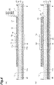
- the polysilicon layer 27a, the silicon nitride layer 28a, the polysilicon layer 27b, the silicon nitride layer 28b, and the polysilicon layer 27c constituting the second laminate 24 are laminated in this order on the intermediate layer 23. More specifically, as illustrated in FIG 5(a) , the second laminate 24 is laminated over the first surface 11a of the portion R so that the surface 23a and the side surface 23b of the intermediate layer 23, the side surface 22a of the first laminate 22, and the side surface 21a of the antireflection layer 21 are covered with the second laminate 24.
- the polysilicon layer and the silicon nitride layer constituting the fourth laminate 44 are laminated on the intermediate layer 43. Subsequently, as illustrated in FIG. 5(b) , by removing the portions of the polysilicon layer 27 other than the polysilicon layer 27a and the silicon nitride layer 28 corresponding to the thinned portion 34b by etching, the peripheral edge portion 34 thinned along the outer edge of the outer edge portion 11c is formed. In addition, in parallel with the lamination of the second laminate 24, the third electrode 14 is formed by doping impurities into the polysilicon layer 27a to partially lower the resistance thereof. Subsequently, terminals 15 and 16 are formed.
- the through holes 24b extending from the surface 24a of the second mirror portion 32 to the removal scheduled portion 50 are formed.
- a light shielding layer 45 is formed on the fourth laminate 44.
- the third laminate 42, the intermediate layer 43, the fourth laminate 44, and the light shielding layer 45 are thinned along the outer edge of the outer edge portion 11c.
- opening 40a is formed in the third laminate 42, the intermediate layer 43, the fourth laminate 44, and the light shielding layer 45.
- the protective layer 46 is formed on the surface of the light shielding layer 45 and on the inner surface of the opening 40a.
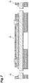
- the removal scheduled portion 50 is removed by gas phase etching through the through holes 24b.
- a hydrofluoric acid gas is used for this gas phase etching.
- the Fabry-Perot interference filter 1 is obtained by cutting the wafer 10 along the outer edge of the outer edge portion 11c in the dicing lines L (fifth step).
- the wafer 10 is cut along the outer edge of the outer edge portion 11c by forming a modified region in an inner portion of the wafer 10 along the outer edge of the outer edge portion 11c by irradiation with a laser beam from the first surface 11a side and by extending a crack in the thickness direction of the wafer 10 from the modified region.
- the removal scheduled portion 50 of the intermediate layer 23 is removed by etching. Therefore, it is possible to suppress deterioration of the intermediate layer 23 at the time of removing the removal scheduled portion 50 by etching. Furthermore, in the method for producing the Fabry-Perot interference filter 1, after forming the second laminate 24 having the peripheral edge portion 34 thinned along the outer edge of the outer edge portion 11c, the Fabry-Perot interference filter 1 is obtained by cutting the wafer 10 along the outer edge of the outer edge portion 11c. Therefore, it is possible to suppress deterioration of each layer on the substrate 11 at the time of cutting the wafer 10.
- the Fabry-Perot interference filter 1 produced by the method for producing the Fabry-Perot interference filter 1 because the intermediate layer 23 is covered with the second laminate 24, peeling of the intermediate layer 23 is suppressed. As described above, according to the method for producing the Fabry-Perot interference filter 1, it is possible to suppress the occurrence of peeling in each layer on the substrate 11.
- the wafer 10 is cut by forming a modified region in an inner portion of the wafer 10 by irradiation with a laser beam and by extending a crack from the modified region in the thickness direction of the wafer 10.
- the thinned portion 34b it is possible to preferably focus the laser beam on an inner portion of the wafer 10, and thus, it is possible to cut the wafer 10 with a high accuracy.
- the peripheral edge portion 34 may be thinned by entirely removing the polysilicon layer 27 and the silicon nitride layer 28 in the thinned portion 34b. In this case, when viewed from the direction perpendicular to the first surface 11a, the outer edge of the peripheral edge portion 34 is positioned inside the outer edge portion of the outer edge portion 11c. In the thinned portion 34b, the polysilicon layer 27 or the silicon nitride layer 28 may be further disposed on the polysilicon layer 27a. That is, the thickness of the portion of the peripheral edge portion 34 along the outer edge of the outer edge portion 11c may be smaller (including zero) than the thickness of the other portion excluding the portion of the peripheral edge portion 34 along the outer edge of the outer edge portion 11c.
- the third laminate 42, the intermediate layer 43, and the fourth laminate 44 may be thinned by removing a portion of each layer in a region overlapping with the thinned portion 34b when viewed from the direction perpendicular to the first surface 11a.
- the thickness of the portions of the third laminate 42, the intermediate layer 43, and the fourth laminate 44 along the outer edge of the outer edge portion 11c may be smaller (including zero) than the thickness of the other portions excluding the portions of the third laminate 42, the intermediate layer 43, and the fourth laminate 44 along the outer edge of the outer edge portion 11c.
- the first laminate 22 may be interposed between the peripheral edge portion 34 and the first surface 11a of the outer edge portion 11c.
- the outer edge of the first laminate 22 when viewed from the direction perpendicular to the first surface 11a, the outer edge of the first laminate 22 may be positioned between the outer edge of the intermediate layer 23 and the outer edge of the outer edge portion 11c and may coincide with the outer edge of the outer edge portion 11c.
- the portion (peripheral edge portion) positioned on the first surface 11a of the outer edge portion 11c in the first laminate 22 may be thinned along the outer edge of the outer edge portion 11c.
- the peripheral edge portion of the first laminate 22 is thinned along the outer edge of the outer edge portion 11c, in a case where the wafer 10 is cut by forming a modified region in an inner portion of the wafer 10 by irradiation with a laser beam and by extending a crack in the thickness direction of the wafer 10 from the modified region, it is possible to more preferably irradiate the inner portion of the wafer 10 with the laser beam.
- the peripheral edge portion 34 does not cover the outer edge of the first laminate 22.
- the Fabry-Perot interference filter 1 may not have a laminate structure (the antireflection layer 41, the third laminate 42, the intermediate layer 43, the fourth laminate 44, the light shielding layer 45, and the protective layer 46) provided on the second surface 11b of the substrate 11.
- the third laminate 42, the intermediate layer 43 and the fourth laminate 44 may not be thinned along the outer edge of the outer edge portion 11c.
- the wafer 10 may be cut by another dicing method such as blade dicing.
- the thinned portion 34b continuously surrounds the non-thinned portion 34a.
- the thinned portion 34b may intermittently surround the non-thinned portion 34a. That is, the peripheral edge portion 34 may be thinned along at least a portion of the outer edge of the outer edge portion 11c.
- the peripheral edge portion 34 may not be thinned along the outer edge of the outer edge portion 11c. Even in this case, because the intermediate layer 23 is covered with the second laminate 24, peeling of the intermediate layer 23 is suppressed. In addition, because the covering portion 33 covers the outer edge of the first laminate 22 and the first laminate 22 is covered with the second laminate 24, peeling of the first laminate 22 is suppressed.
- the outer edge of the polysilicon layer 25c may be positioned inside the outer edge of the first laminate 22 when viewed from the direction perpendicular to the first surface 11a, and the intermediate layer 23 may be interposed between the outer edge of the polysilicon layer 25c and the polysilicon layer 27a.
- Modified Example 1 similarly to the above-described embodiment, it is possible to suppress the occurrence of peeling in each layer on the substrate 11.
- the electrical insulation between the polysilicon layer 25c in which the first electrode 12 is formed and the polysilicon layer 27a in which the third electrode 14 is formed can be enhanced. Therefore, it is possible to suppress the occurrence of leakage of current between the first electrode 12 and the third electrode 14 through the polysilicon layers 25c and 27a. As a result, it is possible to suppress an increase in the voltage applied between the first electrode 12 and the third electrode 14.
- a trench 52 extending annularly so as to surround the terminals 15 and 16 may be provided with the polysilicon layer 27a.
- Modified Example 2 similarly to the above-described embodiment, it is possible to suppress the occurrence of peeling in each layer on the substrate 11.
- the electrical insulation between the polysilicon layer 25c in which the first electrode 12 is formed and the polysilicon layer 27a in which the third electrode 14 is formed can be further enhanced. Therefore, it is possible to further suppress the occurrence of leakage of current between the first electrode 12 and the third electrode 14 through the polysilicon layers 25c and 27a.
- the trench 52 extending annularly so as to surround the terminals 15 and 16 may be provided with the polysilicon layer 27a, and a trench 53 extending annularly so as to surround the terminals 15 and 16 may be provided with the polysilicon layer 25c.
- Modified Example 3 similarly to the above-described embodiment, it is possible to suppress the occurrence of peeling of each layer on the substrate 11.
- the electrical insulation between the polysilicon layer 25c in which the first electrode 12 is formed and the polysilicon layer 27a in which the third electrode 14 is formed can be enhanced. Therefore, it is possible to suppress the occurrence of leakage of current between the first electrode 12 and the third electrode 14 through the polysilicon layers 25c and 27a.
- the outer edge of the first laminate 22 may be positioned inside the outer edge of the intermediate layer 23 when viewed from the direction perpendicular to the first surface 11a, and the intermediate layer 23 may be interposed between the outer edge of the first laminate 22 and the second laminate 24.
- Modified Example 4 similarly to the above-described embodiment, it is possible to suppress the occurrence of peeling of each layer on the substrate 11.
- the electrical insulation between the polysilicon layer 25c in which the first electrode 12 is formed and the polysilicon layer 27a in which the third electrode 14 is formed can be enhanced. As a result, it is possible to effectively suppress the occurrence of leakage of current between the first electrode 12 and the third electrode 14 through the polysilicon layers 25c and 27a.
- the portion covering the outer edge of the first laminate 22 and the intermediate layer 23 in the polysilicon layer 27a may be removed.
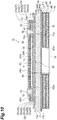
- Modified Example 5 similarly to the above-described embodiment, it is possible to suppress the occurrence of peeling in each layer on the substrate 11.
- the polysilicon layer 25c is covered with the silicon nitride layer 28a, the electrical insulation between the polysilicon layer 25c in which the first electrode 12 is formed and the polysilicon layer 27a in which the third electrode 14 is formed can be enhanced. Therefore, it is possible to suppress the occurrence of leakage of current between the first electrode 12 and the third electrode 14 thourgh the polysilicon layers 25c and 27a.
- Fabry-Perot interference filter 10: wafer, 11: substrate, 11a: first surface, 11b: second surface, 11c: outer edge portion, 22: first laminate (first layer), 23: intermediate layer, 24: second laminate (second layer), 24b: through hole, 31: first mirror portion, 32: second mirror portion, 33: covering portion, 34: peripheral edge portion, 42: third laminate (third layer), 43: intermediate layer (third layer), 44: fourth laminate (third layer), 50: removal scheduled portion, S: air gap.
Landscapes
- Physics & Mathematics (AREA)
- Engineering & Computer Science (AREA)
- Optics & Photonics (AREA)
- Spectroscopy & Molecular Physics (AREA)
- General Physics & Mathematics (AREA)
- Mechanical Engineering (AREA)
- Microelectronics & Electronic Packaging (AREA)
- Plasma & Fusion (AREA)
- Manufacturing & Machinery (AREA)
- Computer Hardware Design (AREA)
- Chemical & Material Sciences (AREA)
- Chemical Kinetics & Catalysis (AREA)
- General Chemical & Material Sciences (AREA)
- Oil, Petroleum & Natural Gas (AREA)
- Mechanical Light Control Or Optical Switches (AREA)
- Micromachines (AREA)
- Optical Filters (AREA)
Abstract
Description
- The present disclosure relates to a Fabry-Perot interference filter and a method for producing a Fabry-Perot interference filter.
- A Fabry-Perot interference filter in the related art includes a substrate, a first layer having a first mirror portion disposed on the substrate, a second layer having a second mirror portion facing the first mirror portion with an air gap interposed therebetween, and an intermediate layer defining the air gap between the first layer and the second layer (refer to, for example, Patent Literature 1).
- Patent Literature 1: Japanese Unexamined Patent Publication No.
2013-257561 - In the Fabry-Perot interference filter as described above, because the respective thicknesses of the first layer, the intermediate layer and the second layer are extremely thin such as, for example, about several tens of nm to several tens of µm, there is a concern that peeling of each layer may occur in use or the like.
- An object of one aspect of the present disclosure is to provide a Fabry-Perot interference filter and a method for producing a Fabry-Perot interference filter, which can suppress the occurrence of peeling in each layer on a substrate.
- A Fabry-Perot interference filter according to one aspect of the present disclosure includes a substrate having a first surface, a first layer having a first mirror portion disposed on a first surface, a second layer having a second mirror portion facing the first mirror portion with an air gap interposed therebetween on a side opposite to the substrate with respect to the first mirror portion, and an intermediate layer defining the air gap between the first layer and the second layer, in which the substrate has an outer edge portion positioned outside an outer edge of the intermediate layer when viewed from a direction perpendicular to the first surface, in which the second layer further includes a covering portion covering the intermediate layer and a peripheral edge portion positioned on the first surface in the outer edge portion, in which the second mirror portion, the covering portion and the peripheral edge portion are integrally formed so as to be continuous with each other, and in which the peripheral edge portion is thinned along the outer edge of the outer edge portion.
- In this Fabry-Perot interference filter, the second layer further includes, in addition to the first mirror portion, a covering portion covering the intermediate layer and a peripheral edge portion positioned on the first surface in the outer edge portion, and the first mirror portion, the covering portion and the peripheral edge portion are integrally formed so as to be continuous with each other. As a result, because the intermediate layer is covered with the second layer, peeling of the intermediate layer is suppressed. In addition, because the intermediate layer is covered with the second layer, deterioration of the intermediate layer is suppressed even in a case where the air gap is formed in the intermediate layer, for example, by etching, so that the stability of the intermediate layer is improved. Furthermore, in this Fabry-Perot interference filter, the peripheral edge portion is thinned along the outer edge of the outer edge portion. Thus, for example, even in a case where the Fabry-Perot interference filter is obtained by cutting the wafer including the portion corresponding to the substrate along the outer edge of the outer edge portion, degradation of each layer on the substrate is suppressed, and as a result, the stability of each layer is improved. As described above, according to the Fabry-Perot interference filter, it is possible to suppress the occurrence of peeling in each layer on the substrate. The phrase "the peripheral edge portion is thinned along the outer edge of the outer edge portion" denotes that "the thickness of the portion of the peripheral edge portion along the outer edge of the outer edge portion is smaller (including zero) than the thickness of the other portions excluding the portion of the peripheral edge portion along the outer edge of the outer edge portion".
- In the Fabry-Perot interference filter according to one aspect of the present disclosure, the covering portion may cover the outer edge of the first layer. According to this, it is possible to more reliably suppress peeling of the first layer. In addition, for example, even in a case where the Fabry-Perot interference filter is obtained by cutting the wafer including the portion corresponding to the substrate along the outer edge of the outer edge portion, it is possible to more preferably suppress degradation of the first layer.
- In the Fabry-Perot interference filter according to one aspect of the present disclosure, the first layer may be a laminate including a silicon nitride layer. According to this, because the silicon nitride layer of the first layer is not exposed to the outside, even in the case of forming an air gap in the intermediate layer by etching using, for example, a hydrofluoric acid gas, it is possible to suppress the generation of residues by reaction of the hydrofluoric acid gas and the silicon nitride layer.
- In the Fabry-Perot interference filter according to one aspect of the present disclosure, the second layer is a laminate including a plurality of layers, and the peripheral edge portion may be thinned along the outer edge of the outer edge portion by removing a portion of the plurality of layers. According to this, it is possible to protect the first surface of the substrate by the remaining portions of the plurality of layers that are not removed.
- The Fabry-Perot interference filter according to one aspect of the present disclosure may further include a third layer disposed on a second surface of the substrate opposing to the first surface. The third layer may be thinned along the outer edge of the outer edge portion. According to this, because the third layer is disposed on the second surface of the substrate, it is possible to suppress warping of the substrate caused by a mismatch in layer configuration between the first surface side and the second surface side of the substrate. In addition, for example, even in a case where the Fabry-Perot interference filter is obtained by cutting the wafer including the portion corresponding to the substrate along the outer edge of the outer edge portion, deterioration of the third layer is suppressed, and as a result, the stability of each layer of the third layer is improved. The phrase "the third layer is thinned along the outer edge of the outer edge portion" denotes that "the thickness of the portion of the third layer along the outer edge of the outer edge portion is smaller (including zero) than the thickness of the other portions excluding the portion of the third layer along the outer edge of the outer edge portion.
- A method for producing a Fabry-Perot interference filter according to one aspect of the present disclosure is a method for producing the Fabry-Perot interference filter, including: a first step of preparing a wafer including a plurality of portions corresponding to the substrate and forming the first layer having the first mirror portion for each of the portions corresponding to the substrate; a second step of forming the intermediate layer having a removal scheduled portion corresponding to the air gap for each of the portions corresponding to the substrate after the first step; a third step of forming the second layer having the second mirror portion a plurality of through holes formed therein, the covering portion covering the intermediate layer, and the peripheral edge portion thinned along the outer edge of the outer edge portion for each of the portions corresponding to the substrate after the second step; a fourth step of forming the air gap positioned between the first mirror portion and the second mirror portion for each of the portions corresponding to the substrate by removing the removal scheduled portion by etching through the through hole after the third step; and a fifth step of obtaining the Fabry-Perot interference filter by cutting the wafer along the outer edge of the outer edge portion after the fourth step.
- In the method for producing the Fabry-Perot interference filter, after forming the second layer having the covering portion covering the intermediate layer, the removal scheduled portion of the intermediate layer is removed by etching. Therefore, it is possible to suppress degradation of the intermediate layer at the time of removing the removal scheduled portion by etching. Furthermore, in the method for producing the Fabry-Perot interference filter, after forming the second layer having the peripheral edge portion thinned along the outer edge of the outer edge portion, the Fabry-Perot interference filter is obtained by cutting the wafer along the outer edge of the outer edge portion. Therefore, it is possible to suppress deterioration of each layer on the substrate at the time of cutting the wafer. In addition, in the Fabry-Perot interference filter produced by the method for producing the Fabry-Perot interference filter, because the intermediate layer is covered with the second layer, peeling of the intermediate layer is suppressed. As described above, according to the method for producing the Fabry-Perot interference filter, it is possible to suppress the occurrence of peeling in each layer on the substrate.
- In the method for producing the Fabry-Perot interference filter according to one aspect of the present disclosure, in the fifth step, the wafer may be cut along the outer edge of the outer edge portion by forming a modified region in an inner portion of the wafer along the outer edge of the outer edge portion by irradiation with a laser beam and by extending a crack from the modified region in a thickness direction of the wafer. According to this, because the peripheral edge portion is thinned along the outer edge of the outer edge portion, it is possible to preferably focus the laser beam on the inner portion of the wafer, and thus, it is possible to cut the wafer with a high accuracy.
- According to one aspect of the present disclosure, it is possible to provide a Fabry-Perot interference filter and a method for producing a Fabry-Perot interference filter, which can suppress the occurrence of peeling in each layer on a substrate.
-
-
FIG. 1 is a plan view of a Fabry-Perot interference filter according to an embodiment of the present disclosure. -
FIG. 2 is a bottom view of the Fabry-Perot interference filter ofFIG. 1 . -
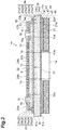
FIG. 3 is a cross-sectional view of the Fabry-Perot interference filter taken along line III-III ofFIG. 1 . -
FIGS. 4(a) and 4(b) are views for describing a method for producing the Fabry-Perot interference filter ofFIG. 1 . -
FIGS. 5(a) and 5(b) are views for describing a method for producing the Fabry-Perot interference filter ofFIG. 1 . -
FIGS. 6(a) and 6(b) are views for describing a method for producing the Fabry-Perot interference filter ofFIG. 1 . -
FIG. 7 is a view for describing a method for producing the Fabry-Perot interference filter ofFIG. 1 . -
FIG. 8(a) is a cross-sectional view of a Fabry-Perot interference filter of Modified Example 1, andFIG. 8(b) is a cross-sectional view of a Fabry-Perot interference filter of Modified Example 2. -
FIG. 9(a) is a cross-sectional view of a Fabry-Perot interference filter of Modified Example 3, andFIG. 9(b) is a cross-sectional view of a Fabry-Perot interference filter of Modified Example 4. -
FIG. 10 is a cross-sectional view of a Fabry-Perot interference filter of Modified Example 5. - Hereinafter, an embodiment of the present disclosure will be described in detail with reference to the drawings. In addition, in the following description, the same reference numerals are used for the same or corresponding elements, and redundant description are omitted.
- As illustrated in
FIGS. 1 ,2 , and3 , the Fabry-Perot interference filter 1 includes asubstrate 11. Thesubstrate 11 has afirst surface 11a and asecond surface 11b opposing to thefirst surface 11a. Anantireflection layer 21, a first laminate (first layer) 22, anintermediate layer 23, and a second laminate (second layer) 24 are laminated in this order on thefirst surface 11a. An air gap S is defined between thefirst laminate 22 and thesecond laminate 24 by a frame-shapedintermediate layer 23. - The shapes and positional relationships of portions when viewed from a direction perpendicular to the
first surface 11a (in plan view) are as follows. The outer edge of thesubstrate 11 has, for example, a rectangular shape. The outer edge of thesubstrate 11 and the outer edge of thesecond laminate 24 coincide with each other. The outer edge of theantireflection layer 21, the outer edge of thefirst laminate 22, and the outer edge of theintermediate layer 23 coincide with each other. Thesubstrate 11 has anouter edge portion 11c positioned outside the outer edge of theintermediate layer 23. Theouter edge portion 11c is, for example, in a frame shape and surrounds theintermediate layer 23 when viewed from the direction perpendicular to thefirst surface 11a. - The Fabry-
Perot interference filter 1 transmits light having a predetermined wavelength in thelight transmission region 1a defined in the central portion thereof. Thelight transmission region 1a is, for example, a cylindrical region. Thesubstrate 11 is made of, for example, silicon, quartz, glass, or the like. In a case where thesubstrate 11 is made of silicon, theantireflection layer 21 and theintermediate layer 23 are made of, for example, a silicon oxide. The thickness of theintermediate layer 23 is, for example, several tens of nm to several tens of µm. - A portion of the
first laminate 22 corresponding to thelight transmission region 1a functions as thefirst mirror portion 31. Thefirst mirror portion 31 is disposed on thefirst surface 11a with theantireflection layer 21 interposed therebetween. Thefirst laminate 22 is configured by alternately laminating a plurality ofpolysilicon layers 25 and a plurality of silicon nitride layers 26 layer by layer. In this embodiment, thepolysilicon layer 25a, thesilicon nitride layer 26a, thepolysilicon layer 25b, thesilicon nitride layer 26b, and thepolysilicon layer 25c are laminated on theantireflection layer 21 in this order. It is preferable that the optical thickness of each of thepolysilicon layer 25 and thesilicon nitride layer 26 constituting thefirst mirror portion 31 is an integral multiple of 1/4 of the center transmission wavelength. Thefirst mirror portion 31 may be disposed directly on thefirst surface 11a without interposing theantireflection layer 21 therebetween. - A portion of the
second laminate 24 corresponding to thelight transmission region 1a functions as thesecond mirror portion 32. Thesecond mirror portion 32 faces thefirst mirror portion 31 with the air gap S interposed therebetween on the side opposite to thesubstrate 11 with respect to thefirst mirror portion 31. Thesecond mirror portion 32 is disposed on thefirst surface 11a with theantireflection layer 21, thefirst laminate 22, and theintermediate layer 23 interposed therebetween. Thesecond laminate 24 is configured by alternately laminating a plurality ofpolysilicon layers 27 and a plurality of silicon nitride layers 28 layer by layer. In this embodiment, thepolysilicon layer 27a, thesilicon nitride layer 28a, thepolysilicon layer 27b, thesilicon nitride layer 28b, and thepolysilicon layer 27c are laminated on theintermediate layer 23 in this order. It is preferable that the optical thickness of each of thepolysilicon layer 27 and thesilicon nitride layer 28 constituting thesecond mirror portion 32 is an integral multiple of 1/4 of the center transmission wavelength. - In the
first laminate 22 and thesecond laminate 24, a silicon oxide layer may be used instead of the silicon nitride layer. In addition, as a material of each layer constituting thefirst laminate 22 and thesecond laminate 24, there may be used a titanium oxide, a tantalum oxide, a zirconium oxide, a magnesium fluoride, an aluminum oxide, a calcium fluoride, silicon, germanium, a zinc sulfide, or the like. - In the
second laminate 24, in a portion corresponding to the air gap S, a plurality of throughholes 24b extending from thesurface 24a of thesecond laminate 24 on the side opposite to theintermediate layer 23 to the air gap S are formed. The plurality of throughholes 24b are formed to such an extent that the through holes do not substantially affect the function of thesecond mirror portion 32. The plurality of throughholes 24b are used to form the air gap S by removing a portion of theintermediate layer 23 by etching. - In addition to the
second mirror portion 32, thesecond laminate 24 further has a coveringportion 33 and aperipheral edge portion 34. Thesecond mirror portion 32, the coveringportion 33, and theperipheral edge portion 34 have the same laminate structure and are integrally formed so as to be continuous with each other. The coveringportion 33 surrounds thesecond mirror portion 32 when viewed from the direction perpendicular to thefirst surface 11a. The coveringportion 33 covers thesurface 23a of theintermediate layer 23 on the side opposite to thesubstrate 11, theside surface 23b of theintermediate layer 23, theside surface 22a of thefirst laminate 22, and theside surface 21a of theantireflection layer 21 and reaches thefirst surface 11a. That is, the coveringportion 33 covers the outer edge of theintermediate layer 23, the outer edge of thefirst laminate 22, and the outer edge of theantireflection layer 21. - The
peripheral edge portion 34 surrounds the coveringportion 33 when viewed from the direction perpendicular to thefirst surface 11a. Theperipheral edge portion 34 is positioned on thefirst surface 11a in theouter edge portion 11c. The outer edge of theperipheral edge portion 34 coincides with the outer edge of thesubstrate 11 when viewed from the direction perpendicular to thefirst surface 11a. - The
peripheral edge portion 34 is thinned along the outer edge of theouter edge portion 11c. That is, the portion of theperipheral edge portion 34 along the outer edge of theouter edge portion 11c is thinner than the other portions excluding the portions of theperipheral edge portion 34 along the outer edge. In this embodiment, theperipheral edge portion 34 is thinned by removing a portion of thepolysilicon layer 27 and thesilicon nitride layer 28 constituting thesecond laminate 24. Theperipheral edge portion 34 has anon-thinned portion 34a continuous with the coveringportion 33 and a thinnedportion 34b surrounding thenon-thinned portion 34a. In the thinnedportion 34b, thepolysilicon layer 27 and thesilicon nitride layer 28 other than thepolysilicon layer 27a directly provided on thefirst surface 11a are removed. - The height of the
surface 34c of thenon-thinned portion 34a on the side opposite to thesubstrate 11 from thefirst surface 11a is lower than the height of thesurface 23a of theintermediate layer 23 from thefirst surface 11a. The height of thesurface 34c of thenon-thinned portion 34a from thefirst surface 11a is, for example, 700 nm to 1400 nm. The height of thesurface 23a of theintermediate layer 23 from thefirst surface 11a is, for example, 2000 nm to 4000 nm. The width of the thinnedportion 34b (the distance between the outer edge of thenon-thinned portion 34a and the outer edge of theouter edge portion 11c) is 0.01 times or more the thickness of thesubstrate 11. The width of the thinnedportion 34b is, for example, 5 µm to 400 µm. The thickness of thesubstrate 11 is, for example, 500 µm to 800 µm. - A
first electrode 12 is formed in thefirst mirror portion 31 so as to surround thelight transmission region 1a. Thefirst electrode 12 is formed by doping impurities into thepolysilicon layer 25c to lower the resistance thereof. Thesecond electrode 13 is formed in thefirst mirror portion 31 so as to include thelight transmission region 1a. Thesecond electrode 13 is formed by doping impurities into thepolysilicon layer 25c to lower the resistance thereof. The size of thesecond electrode 13 is preferably the size including the entirelight transmission region 1a, but may be substantially the same as that of thelight transmission region 1a. - A
third electrode 14 is formed in thesecond mirror portion 32. Thethird electrode 14 faces thefirst electrode 12 and thesecond electrode 13 with the air gap S interposed therebetween. Thethird electrode 14 is formed by doping impurities into thepolysilicon layer 27a to lower the resistance thereof. -
Terminals 15 are provided in a pair so as to face each other with thelight transmission region 1a interposed therebetween. Each terminal 15 is disposed in a through hole extending from thesurface 24a of thesecond laminate 24 to thefirst laminate 22. Each terminal 15 is electrically connected to thefirst electrode 12 via thewiring 12a. -
Terminals 16 are provided in a pair so as to face each other with thelight transmission region 1a interposed therebetween. Each terminal 16 is disposed in a through hole extending from thesurface 24a of thesecond laminate 24 to an inner portion of theintermediate layer 23. Each terminal 16 is electrically connected to thesecond electrode 13 via thewiring 13a and is also electrically connected to thethird electrode 14 via thewiring 14a. The direction in which the pair ofterminals 15 face each other and the direction in which the pair ofterminals 16 face each other are perpendicular to each other (refer toFIG. 1 ). -
Trenches surface 22b of thefirst laminate 22. Thetrench 17 extends annularly so as to surround a portion of thewiring 13a connected to the terminal 16. Thetrench 17 electrically insulates thefirst electrode 12 from thewiring 13a. Thetrench 18 extends annularly along an inner edge of thefirst electrode 12. Thetrench 18 electrically insulates thefirst electrode 12 from the region inside the first electrode 12 (the second electrode 13). The region in each of thetrench - A
trench 19 is provided with thesurface 24a of thesecond laminate 24. Thetrench 19 extends annularly so as to surround the terminal 15. Thetrench 19 electrically insulates the terminal 15 from thethird electrode 14. The region in thetrench 19 may be an insulating material or an air gap. - An
antireflection layer 41, a third laminate (third layer) 42, an intermediate layer (third layer) 43, and a fourth laminate (third layer) 44 are laminated in this order on thesecond surface 11b of thesubstrate 11. Theantireflection layer 41 and theintermediate layer 43 have structures similar to those of theantireflection layer 21 and theintermediate layer 23, respectively. Thethird laminate 42 and thefourth laminate 44 have laminate structures symmetrical to thefirst laminate 22 and thesecond laminate 24 with respect to thesubstrate 11, respectively. Theantireflection layer 41, thethird laminate 42, theintermediate layer 43, and thefourth laminate 44 have a function of suppressing warping of thesubstrate 11. - The
third laminate 42, theintermediate layer 43 and thefourth laminate 44 are thinned along the outer edge of theouter edge portion 11c. That is, the portions of thethird laminate 42, theintermediate layer 43, and thefourth laminate 44 along the outer edge of theouter edge portion 11c are thinner than other portions excluding the portions of thethird laminate 42, theintermediate layer 43, and thefourth laminate 44 along the outer edge. In this embodiment, thethird laminate 42, theintermediate layer 43, and thefourth laminate 44 are thinned by entirely removing thethird laminate 42, theintermediate layer 43, and thefourth laminate 44 in the portions overlapping with the thinnedportion 34b when viewed from the direction perpendicular to thefirst surface 11a. - An
opening 40a is provided with thethird laminate 42, theintermediate layer 43 and thefourth laminate 44 so as to include thelight transmission region 1a. Theopening 40a has substantially the same diameter as the size of thelight transmission region 1a. Theopening 40a is opened to the light emitting side, and the bottom surface of theopening 40a reaches theantireflection layer 41. - A
light shielding layer 45 is formed on the light-emitting-side surface of thefourth laminate 44. Thelight shielding layer 45 is made of, for example, aluminum or the like. Aprotective layer 46 is formed on the surface of thelight shielding layer 45 and the inner surface of theopening 40a. Theprotective layer 46 covers the outer edges of thethird laminate 42, theintermediate layer 43, thefourth laminate 44, and thelight shielding layer 45 and covers theantireflection layer 41 on theouter edge portion 11c. Theprotective layer 46 is made of, for example, an aluminum oxide. It is possible to ignore the optical influence by theprotective layer 46 by setting the thickness of theprotective layer 46 to 1 to 100 nm (preferably about 30 nm). - In the Fabry-
Perot interference filter 1 configured as described above, when a voltage is applied between thefirst electrode 12 and thethird electrode 14 through theterminals first electrode 12 and thethird electrode 14. Due to the electrostatic force, thesecond mirror portion 32 is attracted toward thefirst mirror portion 31 side fixed to thesubstrate 11, and thus, the distance between thefirst mirror portion 31 and thesecond mirror portion 32 is adjusted. As described above, in the Fabry-Perot interference filter 1, the distance between thefirst mirror portion 31 and thesecond mirror portion 32 is variable. - The wavelength of light passing through the Fabry-
Perot interference filter 1 depends on the distance between thefirst mirror portion 31 and thesecond mirror portion 32 in thelight transmission region 1a. Therefore, by adjusting the voltage applied between thefirst electrode 12 and thethird electrode 14, it is possible to appropriately select the wavelength of the transmitting light. At this time, thesecond electrode 13 has the same potential as thethird electrode 14. Therefore, thesecond electrode 13 functions as a compensation electrode for maintaining thefirst mirror portion 31 and thesecond mirror portion 32 flat in thelight transmission region 1a. - In the Fabry-
Perot interference filter 1, for example, while varying the voltage applied to the Fabry-Perot interference filter 1 (that is, changing the distance between thefirst mirror portion 31 and thesecond mirror portion 32 in the Fabry-Perot interference filter 1), by detecting the light transmitted through thelight transmission region 1a of the Fabry-Perot interference filter 1 by a photodetector, it is possible to obtain an optical spectrum. - As described above, in the Fabry-
Perot interference filter 1, thesecond laminate 24 further includes the coveringportion 33 covering theintermediate layer 23 and theperipheral edge portion 34 positioned on thefirst surface 11a in theouter edge portion 11c in addition to thefirst mirror portion 31, and thefirst mirror portion 31, the coveringportion 33, and theperipheral edge portion 34 are integrally formed so as to be continuous with each other. As a result, because theintermediate layer 23 is covered with thesecond laminate 24, it is possible to suppress peeling of theintermediate layer 23. In addition, because theintermediate layer 23 is covered with thesecond laminate 24, even in a case where the air gap S is formed in theintermediate layer 23, for example, by etching, deterioration of theintermediate layer 23 is suppressed, and as a result, the stability of theintermediate layer 23 is improved. Furthermore, in the Fabry-Perot interference filter 1, theperipheral edge portion 34 is thinned along the outer edge of theouter edge portion 11c. Therefore, for example, even in a case where the Fabry-Perot interference filter 1 is obtained by cutting the wafer including the portion corresponding to thesubstrate 11 along the outer edge of theouter edge portion 11c, deterioration of each layer on thesubstrate 11 is suppressed, and as a result, the stability of each layer on the substrate is improved. As described above, according to the Fabry-Perot interference filter 1, it is possible to suppress the occurrence of peeling in each layer on thesubstrate 11. Furthermore, in the Fabry-Perot interference filter 1, because theside surface 23b of theintermediate layer 23 is covered with thesecond laminate 24, it is possible to suppress the incidence of light from theside surface 23b of theintermediate layer 23, and it is possible to suppress the generation of stray light. - In addition, in the Fabry-
Perot interference filter 1, the coveringportion 33 covers the outer edge of thefirst laminate 22. Therefore, it is possible to more reliably suppress peeling of thefirst laminate 22. In addition, for example, even in a case where the Fabry-Perot interference filter 1 is obtained by cutting a wafer including a portion corresponding to thesubstrate 11 along the outer edge of theouter edge portion 11c, it is possible to more preferably suppress deterioration of thefirst laminate 22. - In addition, in the Fabry-
Perot interference filter 1, the outer edge of thesilicon nitride layer 26 included in thefirst laminate 22 is covered with the coveringportion 33. Therefore, because thesilicon nitride layer 26 of thefirst laminate 22 is not exposed to the outside, even in the case of forming the air gap S in theintermediate layer 23 by etching using, for example, a hydrofluoric acid gas, it is possible to suppress the generation of residues by reaction of the hydrofluoric acid gas and thesilicon nitride layer 26. - In addition, the Fabry-
Perot interference filter 1 is thinned along the outer edge of theouter edge portion 11c by removing a portion of thepolysilicon layer 27 and thesilicon nitride layer 28 constituting thesecond laminate 24. Therefore, it is possible to protect thefirst surface 11a of thesubstrate 11 by the remaining portions of thepolysilicon layer 27 and thesilicon nitride layer 28 constituting thesecond laminate 24 that are not removed. Furthermore, in the Fabry-Perot interference filter 1, only thepolysilicon layer 27a remains in the thinnedportion 34b. Therefore, because the surface of the thinnedportion 34b becomes smooth, for example, in order to cut the wafer including the portion corresponding to thesubstrate 11 along the outer edge of theouter edge portion 11c, even in a case where the laser beam is focused on an inner portion of the wafer along the outer edge of theouter edge portion 11c, it is possible to accurately cut the wafer by preferably focusing the laser beam on the inner portion of the wafer, and it is possible to more preferably suppress deterioration of each layer on thesubstrate 11. - In addition, in the Fabry-
Perot interference filter 1, thethird laminate 42 and thefourth laminate 44 are disposed on thesecond surface 11b of thesubstrate 11, and thethird laminate 42 and thefourth laminate 44 are thinned along the outer edge theouter edge portion 11c. Therefore, it is possible to suppress warping of thesubstrate 11 caused by a mismatch in layer configuration between thefirst surface 11a side and thesecond surface 11b side of thesubstrate 11. Furthermore, for example, even in a case where the Fabry-Perot interference filter 1 is obtained by cutting the wafer including the portion corresponding to thesubstrate 11 along the outer edge of theouter edge portion 11c, deterioration of thethird laminate 42 and thefourth laminate 44 is suppressed, and as a result, the stability of each layer on thesubstrate 11 is improved. - Next, an example of a method for producing the Fabry-
Perot interference filter 1 will be described with reference toFIGS. 4 to 7 . First, as illustrated inFIG. 4(a) , awafer 10 including a plurality of portions R corresponding to thesubstrate 11 is prepared, and thefirst laminate 22 having thefirst mirror portion 31 is formed for each of the portions R corresponding to thesubstrates 11 of the wafer 10 (first step). Thewafer 10 is, for example, a silicon wafer. In thewafer 10, the portions R are arranged, for example, in a lattice pattern so as to be adjacent to each other. Dicing lines L are set on the boundary between the portions R. - In the first step, first, the
antireflection layer 21 is formed on thefirst surface 11a of the portion R, and at the same time, theantireflection layer 41 is formed on thesecond surface 11b of the portion R. Subsequently, thepolysilicon layer 25a, thesilicon nitride layer 26a, thepolysilicon layer 25b, thesilicon nitride layer 26b, and thepolysilicon layer 25c constituting thefirst laminate 22 are laminated in this order on theantireflection layer 21. Simultaneously with the lamination of thefirst laminate 22, the polysilicon layer and the silicon nitride layer constituting thethird laminate 42 are laminated on theantireflection layer 41. At the time of lamination of thefirst laminate 22, after thepolysilicon layer 25 and thesilicon nitride layer 26 are laminated over thefirst surface 11a, portions of thepolysilicon layer 25 and thesilicon nitride layer 26, which are positioned on theouter edge portion 11c, when viewed from the direction perpendicular to thefirst surface 11 a are removed by etching. In addition, in parallel with the lamination of thefirst laminate 22, thefirst electrode 12 and thesecond electrode 13 are formed by doping impurities into the polysilicon layers 25b and 25c to partially lower the resistance thereof. Subsequently,trenches - Subsequently, as illustrated in
FIG. 4(b) , theintermediate layer 23 having the removal scheduledportion 50 corresponding to the air gap S is formed for each portion R (second step). In the second step, first, theintermediate layer 23 is formed over thefirst surface 11a of the portion R so that thefirst laminate 22 is covered with theintermediate layer 23. Simultaneously with the formation of theintermediate layer 23, theintermediate layer 43 is formed on thethird laminate 42. Subsequently, the portion of theintermediate layer 23 positioned on theouter edge portion 11c when viewed from the direction perpendicular to thefirst surface 11a is removed by etching. During this etching, the portion of theantireflection layer 21 positioned on theouter edge portion 11c when viewed from the direction perpendicular to thefirst surface 11a is removed. In addition, during this etching, the air gap is formed in the portion corresponding to thewiring 13a andterminals FIG. 3 . - Subsequently, as illustrated in
FIGS. 5(a), 5(b) , and6(a) , thesecond laminate 24 having thesecond mirror portion 32 in which the plurality of throughholes 24b are formed, the coveringportion 33 which covers theintermediate layer 23, and theperipheral edge portion 34 which is thinned along the outer edge of theouter edge portion 11c is formed for each portion R (third step). - In the third step, first, the
polysilicon layer 27a, thesilicon nitride layer 28a, thepolysilicon layer 27b, thesilicon nitride layer 28b, and thepolysilicon layer 27c constituting thesecond laminate 24 are laminated in this order on theintermediate layer 23. More specifically, as illustrated inFIG 5(a) , thesecond laminate 24 is laminated over thefirst surface 11a of the portion R so that thesurface 23a and theside surface 23b of theintermediate layer 23, theside surface 22a of thefirst laminate 22, and theside surface 21a of theantireflection layer 21 are covered with thesecond laminate 24. Simultaneously with the lamination of thesecond laminate 24, the polysilicon layer and the silicon nitride layer constituting thefourth laminate 44 are laminated on theintermediate layer 43. Subsequently, as illustrated inFIG. 5(b) , by removing the portions of thepolysilicon layer 27 other than thepolysilicon layer 27a and thesilicon nitride layer 28 corresponding to the thinnedportion 34b by etching, theperipheral edge portion 34 thinned along the outer edge of theouter edge portion 11c is formed. In addition, in parallel with the lamination of thesecond laminate 24, thethird electrode 14 is formed by doping impurities into thepolysilicon layer 27a to partially lower the resistance thereof. Subsequently,terminals - Subsequently, as illustrated in
FIG. 6(a) , by partially etching thesecond laminate 24, the throughholes 24b extending from thesurface 24a of thesecond mirror portion 32 to the removal scheduledportion 50 are formed. Subsequently, alight shielding layer 45 is formed on thefourth laminate 44. Subsequently, by removing the portions of thethird laminate 42, theintermediate layer 43, thefourth laminate 44, and thelight shielding layer 45 overlapping with the thinnedportion 34b when viewed from the perpendicular direction by etching, thethird laminate 42, theintermediate layer 43 and thefourth laminate 44 are thinned along the outer edge of theouter edge portion 11c. In addition, during this etching,opening 40a is formed in thethird laminate 42, theintermediate layer 43, thefourth laminate 44, and thelight shielding layer 45. Subsequently, theprotective layer 46 is formed on the surface of thelight shielding layer 45 and on the inner surface of theopening 40a. - Subsequently, as illustrated in
FIG. 6(b) , by removing the removal scheduledportion 50 by etching through the throughholes 24b, the air gap positioned between thefirst mirror portion 31 and the second mirror portion 32 S is formed for each portion R (fourth step). In the fourth step, the removal scheduledportion 50 is removed by gas phase etching through the throughholes 24b. For this gas phase etching, for example, a hydrofluoric acid gas is used. - Subsequently, as illustrated in
FIG. 6(b) , the Fabry-Perot interference filter 1 is obtained by cutting thewafer 10 along the outer edge of theouter edge portion 11c in the dicing lines L (fifth step). In the fifth step, for example, thewafer 10 is cut along the outer edge of theouter edge portion 11c by forming a modified region in an inner portion of thewafer 10 along the outer edge of theouter edge portion 11c by irradiation with a laser beam from thefirst surface 11a side and by extending a crack in the thickness direction of thewafer 10 from the modified region. - As described above, in the method for producing the Fabry-
Perot interference filter 1, after forming thesecond laminate 24 having the coveringportion 33 covering theintermediate layer 23, the removal scheduledportion 50 of theintermediate layer 23 is removed by etching. Therefore, it is possible to suppress deterioration of theintermediate layer 23 at the time of removing the removal scheduledportion 50 by etching. Furthermore, in the method for producing the Fabry-Perot interference filter 1, after forming thesecond laminate 24 having theperipheral edge portion 34 thinned along the outer edge of theouter edge portion 11c, the Fabry-Perot interference filter 1 is obtained by cutting thewafer 10 along the outer edge of theouter edge portion 11c. Therefore, it is possible to suppress deterioration of each layer on thesubstrate 11 at the time of cutting thewafer 10. In addition, in the Fabry-Perot interference filter 1 produced by the method for producing the Fabry-Perot interference filter 1, because theintermediate layer 23 is covered with thesecond laminate 24, peeling of theintermediate layer 23 is suppressed. As described above, according to the method for producing the Fabry-Perot interference filter 1, it is possible to suppress the occurrence of peeling in each layer on thesubstrate 11. - In addition, in the method for producing the Fabry-
Perot interference filter 1, thewafer 10 is cut by forming a modified region in an inner portion of thewafer 10 by irradiation with a laser beam and by extending a crack from the modified region in the thickness direction of thewafer 10. By forming the thinnedportion 34b, it is possible to preferably focus the laser beam on an inner portion of thewafer 10, and thus, it is possible to cut thewafer 10 with a high accuracy. - Although an embodiment of the present disclosure has been described above, an aspect of the present disclosure is not limited to the embodiment described above. For example, the materials and shapes of the respective components are not limited to the above-described materials and shapes, and various materials and shapes can be adopted.
- The
peripheral edge portion 34 may be thinned by entirely removing thepolysilicon layer 27 and thesilicon nitride layer 28 in the thinnedportion 34b. In this case, when viewed from the direction perpendicular to thefirst surface 11a, the outer edge of theperipheral edge portion 34 is positioned inside the outer edge portion of theouter edge portion 11c. In the thinnedportion 34b, thepolysilicon layer 27 or thesilicon nitride layer 28 may be further disposed on thepolysilicon layer 27a. That is, the thickness of the portion of theperipheral edge portion 34 along the outer edge of theouter edge portion 11c may be smaller (including zero) than the thickness of the other portion excluding the portion of theperipheral edge portion 34 along the outer edge of theouter edge portion 11c. Thethird laminate 42, theintermediate layer 43, and thefourth laminate 44 may be thinned by removing a portion of each layer in a region overlapping with the thinnedportion 34b when viewed from the direction perpendicular to thefirst surface 11a. In other words, the thickness of the portions of thethird laminate 42, theintermediate layer 43, and thefourth laminate 44 along the outer edge of theouter edge portion 11c may be smaller (including zero) than the thickness of the other portions excluding the portions of thethird laminate 42, theintermediate layer 43, and thefourth laminate 44 along the outer edge of theouter edge portion 11c. - The
first laminate 22 may be interposed between theperipheral edge portion 34 and thefirst surface 11a of theouter edge portion 11c. In this case, when viewed from the direction perpendicular to thefirst surface 11a, the outer edge of thefirst laminate 22 may be positioned between the outer edge of theintermediate layer 23 and the outer edge of theouter edge portion 11c and may coincide with the outer edge of theouter edge portion 11c. In this case, the portion (peripheral edge portion) positioned on thefirst surface 11a of theouter edge portion 11c in thefirst laminate 22 may be thinned along the outer edge of theouter edge portion 11c. According to this configuration, even in a case where the Fabry-Perot interference filter 1 is obtained by cutting thewafer 10 including the portion R corresponding to thesubstrate 11 along the outer edge of theouter edge portion 11c, it is possible to more preferably suppress deterioration of each layer on thesubstrate 11. Furthermore, because the peripheral edge portion of thefirst laminate 22 is thinned along the outer edge of theouter edge portion 11c, in a case where thewafer 10 is cut by forming a modified region in an inner portion of thewafer 10 by irradiation with a laser beam and by extending a crack in the thickness direction of thewafer 10 from the modified region, it is possible to more preferably irradiate the inner portion of thewafer 10 with the laser beam. In a case where the outer edge of thefirst laminate 22 coincides with the outer edge of theouter edge portion 11c, theperipheral edge portion 34 does not cover the outer edge of thefirst laminate 22. - The Fabry-
Perot interference filter 1 may not have a laminate structure (theantireflection layer 41, thethird laminate 42, theintermediate layer 43, thefourth laminate 44, thelight shielding layer 45, and the protective layer 46) provided on thesecond surface 11b of thesubstrate 11. Thethird laminate 42, theintermediate layer 43 and thefourth laminate 44 may not be thinned along the outer edge of theouter edge portion 11c. In the fifth step, thewafer 10 may be cut by another dicing method such as blade dicing. In the above-described embodiment, the thinnedportion 34b continuously surrounds thenon-thinned portion 34a. However, the thinnedportion 34b may intermittently surround thenon-thinned portion 34a. That is, theperipheral edge portion 34 may be thinned along at least a portion of the outer edge of theouter edge portion 11c. - In the above-described embodiment, the
peripheral edge portion 34 may not be thinned along the outer edge of theouter edge portion 11c. Even in this case, because theintermediate layer 23 is covered with thesecond laminate 24, peeling of theintermediate layer 23 is suppressed. In addition, because the coveringportion 33 covers the outer edge of thefirst laminate 22 and thefirst laminate 22 is covered with thesecond laminate 24, peeling of thefirst laminate 22 is suppressed. - As in the Fabry-
Perot interference filter 1A of Modified Example 1 illustrated inFIG. 8(a) , in the Fabry-Perot interference filter 1 of the above-described embodiment, the outer edge of thepolysilicon layer 25c may be positioned inside the outer edge of thefirst laminate 22 when viewed from the direction perpendicular to thefirst surface 11a, and theintermediate layer 23 may be interposed between the outer edge of thepolysilicon layer 25c and thepolysilicon layer 27a. According to Modified Example 1, similarly to the above-described embodiment, it is possible to suppress the occurrence of peeling in each layer on thesubstrate 11. Furthermore, in Modified Example 1, the electrical insulation between thepolysilicon layer 25c in which thefirst electrode 12 is formed and thepolysilicon layer 27a in which thethird electrode 14 is formed can be enhanced. Therefore, it is possible to suppress the occurrence of leakage of current between thefirst electrode 12 and thethird electrode 14 through the polysilicon layers 25c and 27a. As a result, it is possible to suppress an increase in the voltage applied between thefirst electrode 12 and thethird electrode 14. - As in the Fabry-
Perot interference filter 1B of Modified Example 2 illustrated inFIG. 8(b) , in the Fabry-Perot interference filter 1A of Modified Example 1, atrench 52 extending annularly so as to surround theterminals polysilicon layer 27a. According to Modified Example 2, similarly to the above-described embodiment, it is possible to suppress the occurrence of peeling in each layer on thesubstrate 11. Furthermore, in Modified Example 2, the electrical insulation between thepolysilicon layer 25c in which thefirst electrode 12 is formed and thepolysilicon layer 27a in which thethird electrode 14 is formed can be further enhanced. Therefore, it is possible to further suppress the occurrence of leakage of current between thefirst electrode 12 and thethird electrode 14 through the polysilicon layers 25c and 27a. - As in the Fabry-
Perot interference filter 1C of Modified Example 3 illustrated inFIG. 9(a) , in the Fabry-Perot interference filter 1 of the above-described embodiment, thetrench 52 extending annularly so as to surround theterminals polysilicon layer 27a, and atrench 53 extending annularly so as to surround theterminals polysilicon layer 25c. According to Modified Example 3, similarly to the above-described embodiment, it is possible to suppress the occurrence of peeling of each layer on thesubstrate 11. Furthermore, in Modified Example 3, the electrical insulation between thepolysilicon layer 25c in which thefirst electrode 12 is formed and thepolysilicon layer 27a in which thethird electrode 14 is formed can be enhanced. Therefore, it is possible to suppress the occurrence of leakage of current between thefirst electrode 12 and thethird electrode 14 through the polysilicon layers 25c and 27a. - As in the Fabry-
Perot interference filter 1D of Modified Example 4 illustrated inFIG. 9(b) , in the Fabry-Perot interference filter 1 of the above-described embodiment, the outer edge of thefirst laminate 22 may be positioned inside the outer edge of theintermediate layer 23 when viewed from the direction perpendicular to thefirst surface 11a, and theintermediate layer 23 may be interposed between the outer edge of thefirst laminate 22 and thesecond laminate 24. According to Modified Example 4, similarly to the above-described embodiment, it is possible to suppress the occurrence of peeling of each layer on thesubstrate 11. Furthermore, in Modified Example 4, the electrical insulation between thepolysilicon layer 25c in which thefirst electrode 12 is formed and thepolysilicon layer 27a in which thethird electrode 14 is formed can be enhanced. As a result, it is possible to effectively suppress the occurrence of leakage of current between thefirst electrode 12 and thethird electrode 14 through the polysilicon layers 25c and 27a. - As in the Fabry-Perot interference filter IE of Modified Example 5 illustrated in
FIG. 10 , in the Fabry-Perot interference filter 1 of the above-described embodiment, the portion covering the outer edge of thefirst laminate 22 and theintermediate layer 23 in thepolysilicon layer 27a may be removed. According to Modified Example 5, similarly to the above-described embodiment, it is possible to suppress the occurrence of peeling in each layer on thesubstrate 11. Furthermore, in Modified Example 5, because thepolysilicon layer 25c is covered with thesilicon nitride layer 28a, the electrical insulation between thepolysilicon layer 25c in which thefirst electrode 12 is formed and thepolysilicon layer 27a in which thethird electrode 14 is formed can be enhanced. Therefore, it is possible to suppress the occurrence of leakage of current between thefirst electrode 12 and thethird electrode 14 thourgh the polysilicon layers 25c and 27a. - 1: Fabry-Perot interference filter, 10: wafer, 11: substrate, 11a: first surface, 11b: second surface, 11c: outer edge portion, 22: first laminate (first layer), 23: intermediate layer, 24: second laminate (second layer), 24b: through hole, 31: first mirror portion, 32: second mirror portion, 33: covering portion, 34: peripheral edge portion, 42: third laminate (third layer), 43: intermediate layer (third layer), 44: fourth laminate (third layer), 50: removal scheduled portion, S: air gap.
Claims (7)
- A Fabry-Perot interference filter comprising:a substrate having a first surface;a first layer having a first mirror portion disposed on the first surface;a second layer having a second mirror portion facing the first mirror portion with an air gap interposed therebetween on a side opposite to the substrate with respect to the first mirror portion; andan intermediate layer defining the air gap between the first layer and the second layer,wherein the substrate has an outer edge portion positioned outside an outer edge of the intermediate layer when viewed from a direction perpendicular to the first surface,wherein the second layer further includes:a covering portion covering the intermediate layer; anda peripheral edge portion positioned on the first surface in the outer edge portion,wherein the second mirror portion, the covering portion, and the peripheral edge portion are integrally formed so as to be continuous with each other, andwherein the peripheral edge portion is thinned along an outer edge of the outer edge portion.
- The Fabry-Perot interference filter according to claim 1, wherein the covering portion covers an outer edge of the first layer.
- The Fabry-Perot interference filter according to claim 2, wherein the first layer is a laminate including a silicon nitride layer.
- The Fabry-Perot interference filter according to any one of claims 1 to 3,
wherein the second layer is a laminate including a plurality of layers, and
wherein the peripheral edge portion is thinned along the outer edge of the outer edge portion by removing a portion of the plurality of layers. - The Fabry-Perot interference filter according to any one of claims 1 to 4, further comprising a third layer disposed on a second surface of the substrate opposing to the first surface,
wherein the third layer is thinned along the outer edge of the outer edge portion. - A method for producing the Fabry-Perot interference filter according to any one of claims 1 to 5, the method comprising:a first step of preparing a wafer including a plurality of portions corresponding to the substrate and forming the first layer having the first mirror portion for each of the portions corresponding to the substrate;a second step of forming the intermediate layer having a removal scheduled portion corresponding to the air gap for each of the portions corresponding to the substrate after the first step;a third step of forming the second layer having the second mirror portion having a plurality of through holes formed therein, the covering portion covering the intermediate layer, and the peripheral edge portion thinned along the outer edge of the outer edge portion for each of the portions corresponding to the substrate after the second step;a fourth step of forming the air gap positioned between the first mirror portion and the second mirror portion for each of the portions corresponding to the substrate by removing the removal scheduled portion by etching through the through hole after the third step; anda fifth step of obtaining the Fabry-Perot interference filter by cutting the wafer along the outer edge of the outer edge portion after the fourth step.
- The method for producing the Fabry-Perot interference filter according to claim 6, wherein, in the fifth step, the wafer is cut along the outer edge of the outer edge portion by forming a modified region in an inner portion of the wafer along the outer edge of the outer edge portion by irradiation with a laser beam and by extending a crack from the modified region in a thickness direction of the wafer.
Applications Claiming Priority (2)
| Application Number | Priority Date | Filing Date | Title |
|---|---|---|---|
| JP2016106269 | 2016-05-27 | ||
| PCT/JP2017/017172 WO2017203949A1 (en) | 2016-05-27 | 2017-05-01 | Fabry-perot interference filter and production method for fabry-perot interference filter |
Publications (2)
| Publication Number | Publication Date |
|---|---|
| EP3467566A1 true EP3467566A1 (en) | 2019-04-10 |
| EP3467566A4 EP3467566A4 (en) | 2019-12-25 |
Family
ID=60411250
Family Applications (2)
| Application Number | Title | Priority Date | Filing Date |
|---|---|---|---|
| EP17802544.1A Active EP3467565B1 (en) | 2016-05-27 | 2017-05-01 | Production method for fabry-perot interference filter |
| EP17802546.6A Pending EP3467566A4 (en) | 2016-05-27 | 2017-05-01 | FABRY-PEROT INTERFERENCE FILTER AND PROCESS FOR PRODUCING FABRY-PEROT INTERFERENCE FILTER |
Family Applications Before (1)
| Application Number | Title | Priority Date | Filing Date |
|---|---|---|---|
| EP17802544.1A Active EP3467565B1 (en) | 2016-05-27 | 2017-05-01 | Production method for fabry-perot interference filter |
Country Status (10)
| Country | Link |
|---|---|
| US (3) | US10900834B2 (en) |
| EP (2) | EP3467565B1 (en) |
| JP (3) | JP6341959B2 (en) |
| KR (1) | KR102349371B1 (en) |
| CN (2) | CN109313334B (en) |
| CA (1) | CA3024961A1 (en) |
| PH (1) | PH12018502443A1 (en) |
| SG (1) | SG11201807221YA (en) |
| TW (2) | TWI733816B (en) |
| WO (1) | WO2017203949A1 (en) |
Families Citing this family (9)
| Publication number | Priority date | Publication date | Assignee | Title |
|---|---|---|---|---|
| JP6341959B2 (en) | 2016-05-27 | 2018-06-13 | 浜松ホトニクス株式会社 | Manufacturing method of Fabry-Perot interference filter |
| CN109196405B (en) | 2016-05-27 | 2021-09-10 | 浜松光子学株式会社 | Method for producing a Fabry-Perot interference filter |
| JP6899314B2 (en) * | 2017-11-17 | 2021-07-07 | 浜松ホトニクス株式会社 | Adsorption method |
| JP6526771B1 (en) * | 2017-11-24 | 2019-06-05 | 浜松ホトニクス株式会社 | Wafer |
| US20220050238A1 (en) * | 2018-10-03 | 2022-02-17 | Hamamatsu Photonics K.K. | Fabry-perot interference filter |
| JP7202160B2 (en) | 2018-12-05 | 2023-01-11 | 浜松ホトニクス株式会社 | OPTICAL FILTER DEVICE AND CONTROL METHOD FOR OPTICAL FILTER DEVICE |
| JP7464374B2 (en) * | 2019-10-23 | 2024-04-09 | 浜松ホトニクス株式会社 | Manufacturing method of mirror device |
| JP7091489B2 (en) * | 2020-02-26 | 2022-06-27 | キヤノンファインテックニスカ株式会社 | A one-way clutch, a drive transmission unit using this one-way clutch, and an inkjet recording device using this drive transmission unit. |
| DE102020203573A1 (en) | 2020-03-19 | 2021-09-23 | Robert Bosch Gesellschaft mit beschränkter Haftung | Semiconductor substrate and method for forming air and / or gas transfer access through a semiconductor substrate |
Family Cites Families (67)
| Publication number | Priority date | Publication date | Assignee | Title |
|---|---|---|---|---|
| CN1059968A (en) | 1990-09-20 | 1992-04-01 | 托木斯克国立库伊比谢瓦大学 | Interferometric optical filter system selectively |
| US6981804B2 (en) | 1998-06-08 | 2006-01-03 | Arrayed Fiberoptics Corporation | Vertically integrated optical devices coupled to optical fibers |
| CN1085343C (en) | 1998-07-22 | 2002-05-22 | 李韫言 | Infrared Fabry-Perot color filter for micro processing and manufacturing method thereof |
| WO2003007049A1 (en) | 1999-10-05 | 2003-01-23 | Iridigm Display Corporation | Photonic mems and structures |
| US6590710B2 (en) | 2000-02-18 | 2003-07-08 | Yokogawa Electric Corporation | Fabry-Perot filter, wavelength-selective infrared detector and infrared gas analyzer using the filter and detector |
| JP2002174721A (en) | 2000-12-06 | 2002-06-21 | Yokogawa Electric Corp | Fabry-Perot filter |
| US7317531B2 (en) | 2002-12-05 | 2008-01-08 | Kla-Tencor Technologies Corporation | Apparatus and methods for detecting overlay errors using scatterometry |
| US6436794B1 (en) | 2001-05-21 | 2002-08-20 | Hewlett-Packard Company | Process flow for ARS mover using selenidation wafer bonding before processing a media side of a rotor wafer |
| CN101335235B (en) | 2002-03-12 | 2010-10-13 | 浜松光子学株式会社 | Method for dicing substrate |
| US9533376B2 (en) * | 2013-01-15 | 2017-01-03 | Microfabrica Inc. | Methods of forming parts using laser machining |
| WO2004059357A1 (en) | 2002-12-20 | 2004-07-15 | Micron Optics, Inc. | Temperature compensated ferrule holder for a fiber fabry-perot filter |
| WO2004080642A1 (en) | 2003-03-12 | 2004-09-23 | Hamamatsu Photonics K.K. | Laser beam machining method |
| JP2005043726A (en) * | 2003-07-23 | 2005-02-17 | Fuji Photo Film Co Ltd | Display element and portable equipment using it |
| JP4563097B2 (en) | 2003-09-10 | 2010-10-13 | 浜松ホトニクス株式会社 | Semiconductor substrate cutting method |
| JP4166712B2 (en) * | 2004-01-29 | 2008-10-15 | 株式会社デンソー | Fabry-Perot filter |
| US7429334B2 (en) | 2004-09-27 | 2008-09-30 | Idc, Llc | Methods of fabricating interferometric modulators by selectively removing a material |
| US7405108B2 (en) | 2004-11-20 | 2008-07-29 | International Business Machines Corporation | Methods for forming co-planar wafer-scale chip packages |
| JP4587320B2 (en) | 2005-06-30 | 2010-11-24 | 株式会社半導体エネルギー研究所 | Microstructure, micromachine, and manufacturing method thereof |
| EP2495212A3 (en) | 2005-07-22 | 2012-10-31 | QUALCOMM MEMS Technologies, Inc. | Mems devices having support structures and methods of fabricating the same |
| US7502401B2 (en) * | 2005-07-22 | 2009-03-10 | Avago Technologies General Ip (Singapore) Pte. Ltd. | VCSEL system with transverse P/N junction |
| JP2007077864A (en) | 2005-09-14 | 2007-03-29 | Ricoh Co Ltd | Electrostatic actuator, droplet discharge head, liquid cartridge, image forming apparatus, micropump, and optical device |
| DE102006008584A1 (en) | 2006-02-24 | 2007-09-06 | Atmel Germany Gmbh | Manufacturing process for integrated piezo components |
| WO2007107176A1 (en) * | 2006-03-17 | 2007-09-27 | Freescale Semiconductor, Inc. | Method of reducing risk of delamination of a layer of a semiconductor device |
| US20150138642A1 (en) * | 2007-08-12 | 2015-05-21 | Toyota Motor Engineering & Manufacturing North America, Inc. | Durable hybrid omnidirectional structural color pigments for exterior applications |
| JP2009081428A (en) * | 2007-09-03 | 2009-04-16 | Rohm Co Ltd | Semiconductor light emitting device and manufacturing method thereof |
| US7626707B2 (en) * | 2007-10-29 | 2009-12-01 | Symphony Acoustics, Inc. | Dual cavity displacement sensor |
| JP5151444B2 (en) | 2007-12-14 | 2013-02-27 | 株式会社デンソー | Semiconductor chip and manufacturing method thereof |
| JP2008103776A (en) * | 2008-01-18 | 2008-05-01 | Seiko Epson Corp | Dicing method and micromachine device |
| US20100015782A1 (en) | 2008-07-18 | 2010-01-21 | Chen-Hua Yu | Wafer Dicing Methods |
| US8739390B2 (en) | 2008-12-16 | 2014-06-03 | Massachusetts Institute Of Technology | Method for microcontact printing of MEMS |
| US9391423B2 (en) * | 2008-12-16 | 2016-07-12 | Massachusetts Institute Of Technology | Method and applications of thin-film membrane transfer |
| FI125817B (en) * | 2009-01-27 | 2016-02-29 | Teknologian Tutkimuskeskus Vtt Oy | Improved electronically controlled Fabry-Perot interferometer, an intermediate product, an electrode system and a method for producing an electronically controlled Fabry-Perot interferometer |
| JP5276035B2 (en) | 2009-04-13 | 2013-08-28 | 日本電波工業株式会社 | Piezoelectric device manufacturing method and piezoelectric device |
| FI124072B (en) | 2009-05-29 | 2014-03-14 | Valtion Teknillinen | Micromechanical Fabry-Perot Adjustable Interferometer, Intermediate, and Method of Manufacture |
| JP5096425B2 (en) | 2009-07-23 | 2012-12-12 | 日本電波工業株式会社 | Manufacturing method of optical filter |
| FI20095976A0 (en) | 2009-09-24 | 2009-09-24 | Valtion Teknillinen | Micromechanically adjustable Fabry-Perot interferometer and method for its production |
| JP2011181909A (en) * | 2010-02-02 | 2011-09-15 | Mitsubishi Chemicals Corp | Method of manufacturing semiconductor chip |
| JP5531832B2 (en) * | 2010-07-06 | 2014-06-25 | セイコーエプソン株式会社 | Optical filter, optical filter module, spectrophotometer and optical instrument |
| JP5653110B2 (en) | 2010-07-26 | 2015-01-14 | 浜松ホトニクス株式会社 | Chip manufacturing method |
| JP5640549B2 (en) | 2010-08-19 | 2014-12-17 | セイコーエプソン株式会社 | Optical filter, optical filter manufacturing method, and optical device |
| EP2699952A4 (en) | 2011-04-20 | 2015-06-24 | Univ Michigan | SPECTRAL FILTERING FOR VISUAL DISPLAYS AND IMAGING SYSTEM HAVING MINIMUM ANGULAR DEPENDENCY |
| FI125897B (en) * | 2011-06-06 | 2016-03-31 | Teknologian Tutkimuskeskus Vtt Oy | Micromechanically adjustable Fabry-Perot interferometer and method for manufacturing the same |
| JP5939752B2 (en) | 2011-09-01 | 2016-06-22 | 株式会社ディスコ | Wafer dividing method |
| JP5910099B2 (en) * | 2012-01-18 | 2016-04-27 | セイコーエプソン株式会社 | Interference filters, optical modules and electronics |
| JP5966405B2 (en) | 2012-02-14 | 2016-08-10 | セイコーエプソン株式会社 | Optical filter device and method of manufacturing optical filter device |
| US8884725B2 (en) | 2012-04-19 | 2014-11-11 | Qualcomm Mems Technologies, Inc. | In-plane resonator structures for evanescent-mode electromagnetic-wave cavity resonators |
| FI125368B (en) | 2012-06-08 | 2015-09-15 | Teknologian Tutkimuskeskus Vtt Oy | Micromechanically tunable Fabry-Perot interferometer system and method for producing this |
| US9040389B2 (en) | 2012-10-09 | 2015-05-26 | Infineon Technologies Ag | Singulation processes |
| US20140160137A1 (en) * | 2012-12-12 | 2014-06-12 | Qualcomm Mems Technologies, Inc. | Field-sequential color mode transitions |
| JP6211315B2 (en) | 2013-07-02 | 2017-10-11 | 浜松ホトニクス株式会社 | Fabry-Perot interference filter |
| JP6211833B2 (en) | 2013-07-02 | 2017-10-11 | 浜松ホトニクス株式会社 | Fabry-Perot interference filter |
| JP6264810B2 (en) | 2013-09-27 | 2018-01-24 | セイコーエプソン株式会社 | Interference filter, optical filter device, optical module, and electronic apparatus |
| JP6196867B2 (en) | 2013-10-01 | 2017-09-13 | 浜松ホトニクス株式会社 | Optical module |
| US10184832B2 (en) | 2013-10-31 | 2019-01-22 | Hamamatsu Photonics K.K. | Light-detecting device |
| JP6356427B2 (en) * | 2014-02-13 | 2018-07-11 | 浜松ホトニクス株式会社 | Fabry-Perot interference filter |
| JP6353683B2 (en) * | 2014-04-04 | 2018-07-04 | 浜松ホトニクス株式会社 | Laser processing apparatus and laser processing method |
| CA3194688A1 (en) | 2014-06-18 | 2015-12-23 | Viavi Solutions, Inc. | Metal-dielectric optical filter, sensor device, and fabrication method |
| JP2016099583A (en) * | 2014-11-26 | 2016-05-30 | セイコーエプソン株式会社 | Interference filter, optical module, electronic device, and manufacturing method of structure |
| JP2016163942A (en) | 2015-03-06 | 2016-09-08 | セイコーエプソン株式会社 | Medium conveying device, image reading device |
| JP6034900B2 (en) | 2015-03-06 | 2016-11-30 | ファナック株式会社 | Robot control device for judging resumption of operation program |
| JP2016163916A (en) | 2015-03-06 | 2016-09-08 | 株式会社Ihiエスキューブ | Monitoring device |
| AR105372A1 (en) | 2015-07-27 | 2017-09-27 | Dow Global Technologies Llc | ELASTIC LAMINATES, METHODS FOR MANUFACTURING AND ARTICLES THAT UNDERSTAND THEM |
| EP3328452B1 (en) | 2015-07-28 | 2020-12-09 | CeramTec GmbH | Metallic and/or ceramic components with at least one osseointegrative and osteoinductive surface (multi)layer structure |
| JP6341959B2 (en) * | 2016-05-27 | 2018-06-13 | 浜松ホトニクス株式会社 | Manufacturing method of Fabry-Perot interference filter |
| CN109196405B (en) * | 2016-05-27 | 2021-09-10 | 浜松光子学株式会社 | Method for producing a Fabry-Perot interference filter |
| CN118091929A (en) * | 2016-08-24 | 2024-05-28 | 浜松光子学株式会社 | Fabry-Perot interference filter |
| US10838195B2 (en) * | 2016-08-24 | 2020-11-17 | Hamamatsu Photonics K.K. | Fabry-Perot interference filter |
-
2016
- 2016-08-24 JP JP2016163928A patent/JP6341959B2/en active Active
-
2017
- 2017-05-01 CA CA3024961A patent/CA3024961A1/en not_active Abandoned
- 2017-05-01 US US16/303,209 patent/US10900834B2/en active Active
- 2017-05-01 CN CN201780032566.4A patent/CN109313334B/en active Active
- 2017-05-01 WO PCT/JP2017/017172 patent/WO2017203949A1/en not_active Ceased
- 2017-05-01 SG SG11201807221YA patent/SG11201807221YA/en unknown
- 2017-05-01 EP EP17802544.1A patent/EP3467565B1/en active Active
- 2017-05-01 KR KR1020187024826A patent/KR102349371B1/en active Active
- 2017-05-01 JP JP2018519165A patent/JP6983767B2/en active Active
- 2017-05-01 EP EP17802546.6A patent/EP3467566A4/en active Pending
- 2017-05-01 US US16/065,856 patent/US10908022B2/en active Active
- 2017-05-01 CN CN201780032540.XA patent/CN109196404B/en active Active
- 2017-05-26 TW TW106117484A patent/TWI733816B/en active
- 2017-05-26 TW TW106117483A patent/TWI735581B/en active
-
2018
- 2018-05-15 JP JP2018093874A patent/JP6368447B1/en active Active
- 2018-11-20 PH PH12018502443A patent/PH12018502443A1/en unknown
-
2020
- 2020-12-18 US US17/126,297 patent/US12392661B2/en active Active
Also Published As
| Publication number | Publication date |
|---|---|
| TWI735581B (en) | 2021-08-11 |
| JP2018128703A (en) | 2018-08-16 |
| US10900834B2 (en) | 2021-01-26 |
| EP3467566A4 (en) | 2019-12-25 |
| CN109313334B (en) | 2021-08-17 |
| PH12018502443A1 (en) | 2019-09-09 |
| TW201805686A (en) | 2018-02-16 |
| KR102349371B1 (en) | 2022-01-11 |
| EP3467565A4 (en) | 2020-03-11 |
| JP6368447B1 (en) | 2018-08-01 |
| CA3024961A1 (en) | 2017-11-30 |
| JPWO2017203949A1 (en) | 2019-03-22 |
| US20210131870A1 (en) | 2021-05-06 |
| KR20190012139A (en) | 2019-02-08 |
| EP3467565A1 (en) | 2019-04-10 |
| TWI733816B (en) | 2021-07-21 |
| JP6341959B2 (en) | 2018-06-13 |
| JP6983767B2 (en) | 2021-12-17 |
| US12392661B2 (en) | 2025-08-19 |
| TW201800728A (en) | 2018-01-01 |
| SG11201807221YA (en) | 2018-09-27 |
| EP3467565B1 (en) | 2024-02-14 |
| WO2017203949A1 (en) | 2017-11-30 |
| US10908022B2 (en) | 2021-02-02 |
| CN109313334A (en) | 2019-02-05 |
| US20190204150A1 (en) | 2019-07-04 |
| JP2017215559A (en) | 2017-12-07 |
| CN109196404A (en) | 2019-01-11 |
| US20180373021A1 (en) | 2018-12-27 |
| CN109196404B (en) | 2022-05-03 |
Similar Documents
| Publication | Publication Date | Title |
|---|---|---|
| US10900834B2 (en) | Fabry-Perot interference filter having layer with thinned edge portion and production method for Fabry-Perot interference filter | |
| US10838195B2 (en) | Fabry-Perot interference filter | |
| CN109196405B (en) | Method for producing a Fabry-Perot interference filter | |
| US10724902B2 (en) | Fabry-Perot interference filter | |
| US20250334448A1 (en) | Production method for fabry-perot interference filter |
Legal Events
| Date | Code | Title | Description |
|---|---|---|---|
| STAA | Information on the status of an ep patent application or granted ep patent |
Free format text: STATUS: THE INTERNATIONAL PUBLICATION HAS BEEN MADE |
|
| PUAI | Public reference made under article 153(3) epc to a published international application that has entered the european phase |
Free format text: ORIGINAL CODE: 0009012 |
|
| STAA | Information on the status of an ep patent application or granted ep patent |
Free format text: STATUS: REQUEST FOR EXAMINATION WAS MADE |
|
| 17P | Request for examination filed |
Effective date: 20181203 |
|
| AK | Designated contracting states |
Kind code of ref document: A1 Designated state(s): AL AT BE BG CH CY CZ DE DK EE ES FI FR GB GR HR HU IE IS IT LI LT LU LV MC MK MT NL NO PL PT RO RS SE SI SK SM TR |
|
| AX | Request for extension of the european patent |
Extension state: BA ME |
|
| DAV | Request for validation of the european patent (deleted) | ||
| DAX | Request for extension of the european patent (deleted) | ||
| A4 | Supplementary search report drawn up and despatched |
Effective date: 20191126 |
|
| RIC1 | Information provided on ipc code assigned before grant |
Ipc: B23K 103/00 20060101ALN20191120BHEP Ipc: B81C 1/00 20060101ALI20191120BHEP Ipc: G01J 3/26 20060101ALI20191120BHEP Ipc: B23K 26/00 20140101ALI20191120BHEP Ipc: G02B 26/00 20060101AFI20191120BHEP Ipc: B23K 26/53 20140101ALI20191120BHEP Ipc: B81B 3/00 20060101ALI20191120BHEP Ipc: B23K 26/064 20140101ALI20191120BHEP Ipc: B23K 101/40 20060101ALN20191120BHEP |
|
| STAA | Information on the status of an ep patent application or granted ep patent |
Free format text: STATUS: EXAMINATION IS IN PROGRESS |
|
| 17Q | First examination report despatched |
Effective date: 20211220 |