EP3467565A1 - Production method for fabry-perot interference filter - Google Patents
Production method for fabry-perot interference filter Download PDFInfo
- Publication number
- EP3467565A1 EP3467565A1 EP17802544.1A EP17802544A EP3467565A1 EP 3467565 A1 EP3467565 A1 EP 3467565A1 EP 17802544 A EP17802544 A EP 17802544A EP 3467565 A1 EP3467565 A1 EP 3467565A1
- Authority
- EP
- European Patent Office
- Prior art keywords
- layer
- mirror
- wafer
- fabry
- lines
- Prior art date
- Legal status (The legal status is an assumption and is not a legal conclusion. Google has not performed a legal analysis and makes no representation as to the accuracy of the status listed.)
- Granted
Links
Images




Classifications
-
- G—PHYSICS
- G01—MEASURING; TESTING
- G01J—MEASUREMENT OF INTENSITY, VELOCITY, SPECTRAL CONTENT, POLARISATION, PHASE OR PULSE CHARACTERISTICS OF INFRARED, VISIBLE OR ULTRAVIOLET LIGHT; COLORIMETRY; RADIATION PYROMETRY
- G01J3/00—Spectrometry; Spectrophotometry; Monochromators; Measuring colours
- G01J3/12—Generating the spectrum; Monochromators
- G01J3/26—Generating the spectrum; Monochromators using multiple reflection, e.g. Fabry-Perot interferometer, variable interference filters
-
- G—PHYSICS
- G02—OPTICS
- G02B—OPTICAL ELEMENTS, SYSTEMS OR APPARATUS
- G02B26/00—Optical devices or arrangements for the control of light using movable or deformable optical elements
-
- B—PERFORMING OPERATIONS; TRANSPORTING
- B23—MACHINE TOOLS; METAL-WORKING NOT OTHERWISE PROVIDED FOR
- B23K—SOLDERING OR UNSOLDERING; WELDING; CLADDING OR PLATING BY SOLDERING OR WELDING; CUTTING BY APPLYING HEAT LOCALLY, e.g. FLAME CUTTING; WORKING BY LASER BEAM
- B23K26/00—Working by laser beam, e.g. welding, cutting or boring
- B23K26/0006—Working by laser beam, e.g. welding, cutting or boring taking account of the properties of the material involved
-
- B—PERFORMING OPERATIONS; TRANSPORTING
- B23—MACHINE TOOLS; METAL-WORKING NOT OTHERWISE PROVIDED FOR
- B23K—SOLDERING OR UNSOLDERING; WELDING; CLADDING OR PLATING BY SOLDERING OR WELDING; CUTTING BY APPLYING HEAT LOCALLY, e.g. FLAME CUTTING; WORKING BY LASER BEAM
- B23K26/00—Working by laser beam, e.g. welding, cutting or boring
- B23K26/02—Positioning or observing the workpiece, e.g. with respect to the point of impact; Aligning, aiming or focusing the laser beam
- B23K26/06—Shaping the laser beam, e.g. by masks or multi-focusing
- B23K26/064—Shaping the laser beam, e.g. by masks or multi-focusing by means of optical elements, e.g. lenses, mirrors or prisms
-
- B—PERFORMING OPERATIONS; TRANSPORTING
- B23—MACHINE TOOLS; METAL-WORKING NOT OTHERWISE PROVIDED FOR
- B23K—SOLDERING OR UNSOLDERING; WELDING; CLADDING OR PLATING BY SOLDERING OR WELDING; CUTTING BY APPLYING HEAT LOCALLY, e.g. FLAME CUTTING; WORKING BY LASER BEAM
- B23K26/00—Working by laser beam, e.g. welding, cutting or boring
- B23K26/02—Positioning or observing the workpiece, e.g. with respect to the point of impact; Aligning, aiming or focusing the laser beam
- B23K26/06—Shaping the laser beam, e.g. by masks or multi-focusing
- B23K26/064—Shaping the laser beam, e.g. by masks or multi-focusing by means of optical elements, e.g. lenses, mirrors or prisms
- B23K26/0643—Shaping the laser beam, e.g. by masks or multi-focusing by means of optical elements, e.g. lenses, mirrors or prisms comprising mirrors
-
- B—PERFORMING OPERATIONS; TRANSPORTING
- B23—MACHINE TOOLS; METAL-WORKING NOT OTHERWISE PROVIDED FOR
- B23K—SOLDERING OR UNSOLDERING; WELDING; CLADDING OR PLATING BY SOLDERING OR WELDING; CUTTING BY APPLYING HEAT LOCALLY, e.g. FLAME CUTTING; WORKING BY LASER BEAM
- B23K26/00—Working by laser beam, e.g. welding, cutting or boring
- B23K26/50—Working by transmitting the laser beam through or within the workpiece
- B23K26/53—Working by transmitting the laser beam through or within the workpiece for modifying or reforming the material inside the workpiece, e.g. for producing break initiation cracks
-
- B—PERFORMING OPERATIONS; TRANSPORTING
- B81—MICROSTRUCTURAL TECHNOLOGY
- B81B—MICROSTRUCTURAL DEVICES OR SYSTEMS, e.g. MICROMECHANICAL DEVICES
- B81B3/00—Devices comprising flexible or deformable elements, e.g. comprising elastic tongues or membranes
-
- B—PERFORMING OPERATIONS; TRANSPORTING
- B81—MICROSTRUCTURAL TECHNOLOGY
- B81B—MICROSTRUCTURAL DEVICES OR SYSTEMS, e.g. MICROMECHANICAL DEVICES
- B81B3/00—Devices comprising flexible or deformable elements, e.g. comprising elastic tongues or membranes
- B81B3/0064—Constitution or structural means for improving or controlling the physical properties of a device
- B81B3/0067—Mechanical properties
- B81B3/0072—For controlling internal stress or strain in moving or flexible elements, e.g. stress compensating layers
-
- B—PERFORMING OPERATIONS; TRANSPORTING
- B81—MICROSTRUCTURAL TECHNOLOGY
- B81C—PROCESSES OR APPARATUS SPECIALLY ADAPTED FOR THE MANUFACTURE OR TREATMENT OF MICROSTRUCTURAL DEVICES OR SYSTEMS
- B81C1/00—Manufacture or treatment of devices or systems in or on a substrate
-
- B—PERFORMING OPERATIONS; TRANSPORTING
- B81—MICROSTRUCTURAL TECHNOLOGY
- B81C—PROCESSES OR APPARATUS SPECIALLY ADAPTED FOR THE MANUFACTURE OR TREATMENT OF MICROSTRUCTURAL DEVICES OR SYSTEMS
- B81C1/00—Manufacture or treatment of devices or systems in or on a substrate
- B81C1/00436—Shaping materials, i.e. techniques for structuring the substrate or the layers on the substrate
- B81C1/00523—Etching material
- B81C1/00539—Wet etching
-
- B—PERFORMING OPERATIONS; TRANSPORTING
- B81—MICROSTRUCTURAL TECHNOLOGY
- B81C—PROCESSES OR APPARATUS SPECIALLY ADAPTED FOR THE MANUFACTURE OR TREATMENT OF MICROSTRUCTURAL DEVICES OR SYSTEMS
- B81C1/00—Manufacture or treatment of devices or systems in or on a substrate
- B81C1/00436—Shaping materials, i.e. techniques for structuring the substrate or the layers on the substrate
- B81C1/00634—Processes for shaping materials not provided for in groups B81C1/00444 - B81C1/00626
-
- G—PHYSICS
- G01—MEASURING; TESTING
- G01J—MEASUREMENT OF INTENSITY, VELOCITY, SPECTRAL CONTENT, POLARISATION, PHASE OR PULSE CHARACTERISTICS OF INFRARED, VISIBLE OR ULTRAVIOLET LIGHT; COLORIMETRY; RADIATION PYROMETRY
- G01J3/00—Spectrometry; Spectrophotometry; Monochromators; Measuring colours
- G01J3/02—Details
- G01J3/0205—Optical elements not provided otherwise, e.g. optical manifolds, diffusers, windows
- G01J3/0243—Optical elements not provided otherwise, e.g. optical manifolds, diffusers, windows having a through-hole enabling the optical element to fulfil an additional optical function, e.g. a mirror or grating having a throughhole for a light collecting or light injecting optical fiber
-
- G—PHYSICS
- G02—OPTICS
- G02B—OPTICAL ELEMENTS, SYSTEMS OR APPARATUS
- G02B26/00—Optical devices or arrangements for the control of light using movable or deformable optical elements
- G02B26/001—Optical devices or arrangements for the control of light using movable or deformable optical elements based on interference in an adjustable optical cavity
-
- G—PHYSICS
- G02—OPTICS
- G02B—OPTICAL ELEMENTS, SYSTEMS OR APPARATUS
- G02B5/00—Optical elements other than lenses
- G02B5/20—Filters
- G02B5/28—Interference filters
- G02B5/284—Interference filters of etalon type comprising a resonant cavity other than a thin solid film, e.g. gas, air, solid plates
-
- B—PERFORMING OPERATIONS; TRANSPORTING
- B23—MACHINE TOOLS; METAL-WORKING NOT OTHERWISE PROVIDED FOR
- B23K—SOLDERING OR UNSOLDERING; WELDING; CLADDING OR PLATING BY SOLDERING OR WELDING; CUTTING BY APPLYING HEAT LOCALLY, e.g. FLAME CUTTING; WORKING BY LASER BEAM
- B23K2101/00—Articles made by soldering, welding or cutting
- B23K2101/36—Electric or electronic devices
- B23K2101/40—Semiconductor devices
-
- B—PERFORMING OPERATIONS; TRANSPORTING
- B23—MACHINE TOOLS; METAL-WORKING NOT OTHERWISE PROVIDED FOR
- B23K—SOLDERING OR UNSOLDERING; WELDING; CLADDING OR PLATING BY SOLDERING OR WELDING; CUTTING BY APPLYING HEAT LOCALLY, e.g. FLAME CUTTING; WORKING BY LASER BEAM
- B23K2103/00—Materials to be soldered, welded or cut
- B23K2103/50—Inorganic materials other than metals or composite materials
- B23K2103/56—Inorganic materials other than metals or composite materials being semiconducting
Definitions
- the present disclosure relates to a method of manufacturing a Fabry-Perot interference filter.
- a Fabry-Perot interference filter which includes a substrate, a fixed mirror and a movable mirror facing each other with a gap interposed therebetween on the substrate, and an intermediate layer defining the gap, is known (for example, refer to Patent Literature 1).
- Patent Literature 1 Japanese Unexamined Patent Publication No. 2013-506154
- a Fabry-Perot interference filter as described above is a fine structure, it is difficult to improve both manufacturing efficiency and a yield when a Fabry-Perot interference filter is manufactured.
- an object of the present disclosure is to provide a method of manufacturing a Fabry-Perot interference filter, in which both manufacturing efficiency and a yield can be improved.
- a method of manufacturing a Fabry-Perot interference filter including a forming step of forming a first thinned region in the forming step, a first mirror layer having a plurality of first mirror portions each of which is expected to function as a fixed mirror, a sacrificial layer having a plurality of portions expected to be removed, and a second mirror layer having a plurality of second mirror portions each of which is expected to function as a movable mirror are formed on a first main surface of a wafer expected to be cut into a plurality of substrates along each of a plurality of lines such that one first mirror portion, one portion expected to be removed, and one second mirror portion are disposed in this order from one substrate side, and the first thinned region in which at least one of the first mirror layer, the sacrificial layer, and the second mirror layer is partially thinned along each of the plurality of lines is formed; a cutting step of cutting the wafer into the plurality of substrate
- the modified region is formed within the wafer along each of the lines through irradiation of a laser light. Accordingly, scattering or the like of a laser light is prevented so that the modified region can be reliably formed within the wafer.
- the "first thinned region” includes a region from which all of the parts along each of the lines in the first mirror layer, the sacrificial layer, and the second mirror layer are removed.
- a stress adjustment layer may be formed on a second main surface of the wafer, and a second thinned region in which the stress adjustment layer is partially thinned along each of the plurality of lines may be formed.
- a stress adjustment layer is partially thinned along each of the lines, it is possible to prevent damage from being caused in the stress adjustment layer when a wafer is cut into a plurality of substrates along each of the lines.
- the "second thinned region” includes a region from which all of the parts along each of the lines in the stress adjustment layer are removed.
- the crack in the method of manufacturing a Fabry-Perot interference filter, in the cutting step, the crack may be extended in the thickness direction of the wafer from the modified region by expanding an expanding tape attached to the stress adjustment layer side.
- the crack since an expanding force of the expanding tape is likely to be concentrated in the modified region and a part in the vicinity thereof due to the presence of the second thinned region, the crack can be easily extended in the thickness direction of the wafer from the modified region.
- the laser light in the cutting step, in a state in which the expanding tape is attached to the stress adjustment layer side, the laser light may be incident on the wafer from a side opposite to the expanding tape. According to this configuration, scattering, attenuation, or the like of a laser light caused by the expanding tape is prevented so that the modified region can be reliably formed within the wafer along each of the lines.
- the laser light may be incident on the wafer through the expanding tape from the expanding tape side.
- the expanding tape functions as a cover. Therefore, it is possible to prevent such particles from adhering to the second mirror layer or the like.
- the removing step may be carried out between the forming step and the cutting step.
- the removing step of removing the portion expected to be removed from the sacrificial layer through etching is carried out at wafer level, compared to a case in which the removing step is individually carried out at chip level, it is possible to form a gap between the first mirror portion and the second mirror portion in a remarkably efficient way.
- the following cutting step is carried out through irradiation of a laser light. Therefore, it is possible to effectively prevent a situation in which the second mirror portions floating in the gap become damaged.
- a Fabry-Perot interference filter in the method of manufacturing a Fabry-Perot interference filter, in the forming step, after a part along each of the plurality of lines in the sacrificial layer formed on the first mirror layer is thinned, side surfaces of the sacrificial layer facing each other along each of the plurality of lines may be covered with the second mirror layer by forming the second mirror layer on the sacrificial layer. According to this configuration, it is possible to prevent a part of the side surfaces of the sacrificial layer from being removed when the portion expected to be removed is removed from the sacrificial layer through etching. Moreover, in a manufactured Fabry-Perot interference filter, it is possible to prevent light which becomes stray light from being incident from the side surface of an intermediate layer corresponding to the side surface of the sacrificial layer.
- a part along each of the plurality of lines in at least one of the first mirror layer, the sacrificial layer, and the second mirror layer may be thinned such that a surface of at least one layer configuring the first mirror layer or the second mirror layer is exposed.
- the laser light may be incident on the wafer through the surface of the layer.
- a Fabry-Perot interference filter 1 includes a substrate 11.
- the substrate 11 has a first surface 11a and a second surface 11b facing the first surface 11a.
- a reflection prevention layer 21 On the first surface 11a, a reflection prevention layer 21, a first laminate (first layer) 22, an intermediate layer 23, and a second laminate (second layer) 24 are laminated in this order.
- a gap (air gap) S is defined between the first laminate 22 and the second laminate 24 by the frame-shaped intermediate layer 23.
- an outer edge of the substrate 11 has a rectangular shape.
- the outer edge of the substrate 11 and an outer edge of the second laminate 24 coincide with each other.
- An outer edge of the reflection prevention layer 21, an outer edge of the first laminate 22, and an outer edge of the intermediate layer 23 coincide with each other.
- the substrate 11 has an outer edge portion 11c positioned on an outer side of the outer edge of the intermediate layer 23 with respect to the center of the gap S.
- the outer edge portion 11c has a frame shape and surrounds the intermediate layer 23 in a case of being seen in a direction perpendicular to the first surface 11a.
- the Fabry-Perot interference filter 1 light having a predetermined wavelength is transmitted through a light transmission region 1a defined in a center portion thereof.
- the light transmission region 1a is a columnar region.
- the substrate 11 is made of silicon, quartz, or glass.
- the reflection prevention layer 21 and the intermediate layer 23 are made of silicon oxide, for example.
- the thickness of the intermediate layer 23 ranges from several tens of nm to several tens of ⁇ m, for example.
- a part corresponding to the light transmission region 1a in the first laminate 22 functions as a first mirror portion 31.
- the first mirror portion 31 is disposed on the first surface 11a with the reflection prevention layer 21 interposed therebetween.
- the first laminate 22 is configured to have a plurality of polysilicon layers 25 and a plurality of silicon nitride layers 26 which are alternately laminated one by one.
- a polysilicon layer 25a, a silicon nitride layer 26a, a polysilicon layer 25b, a silicon nitride layer 26b, and a polysilicon layer 25c are laminated on the reflection prevention layer 21 in this order.
- each of the polysilicon layer 25 and the silicon nitride layer 26 configuring the first mirror portion 31 is preferably an integral multiple of 1/4 of a center transmission wavelength.
- the first mirror portion 31 may be directly disposed on the first surface 11a without the reflection prevention layer 21 interposed therebetween.
- a part corresponding to the light transmission region 1a in the second laminate 24 functions as a second mirror portion 32.
- the second mirror portion 32 faces the first mirror portion 31 with the gap S interposed therebetween on a side opposite to the substrate 11 with respect to the first mirror portion 31.
- the second laminate 24 is disposed on the first surface 11a with the reflection prevention layer 21, the first laminate 22, and the intermediate layer 23 interposed therebetween.
- the second laminate 24 is configured to include a plurality of polysilicon layers 27 and a plurality of silicon nitride layers 28 which are alternately laminated one by one.
- a polysilicon layer 27a, a silicon nitride layer 28a, a polysilicon layer 27b, a silicon nitride layer 28b, and a polysilicon layer 27c are laminated on the intermediate layer 23 in this order.
- the optical thickness of each of the polysilicon layer 27 and the silicon nitride layer 28 configuring the second mirror portion 32 is preferably an integral multiple of 1/4 of the center transmission wavelength.
- silicon oxide layers may be used in place of the silicon nitride layers.
- titanium oxide, tantalum oxide, zirconium oxide, magnesium fluoride, aluminum oxide, calcium fluoride, silicon, germanium, zinc sulfide, or the like may be used as the material of each layer configuring the first laminate 22 and the second laminate 24.
- a plurality of through-holes 24b leading from a surface 24a of the second laminate 24 on a side opposite to the intermediate layer 23 to the gap S are formed.
- the plurality of through-holes 24b are formed so as not to substantially affect the function of the second mirror portion 32.
- the plurality of through-holes 24b are used for forming the gap S by removing a part of the intermediate layer 23 through etching.
- the second laminate 24 further has a covering portion 33 and a peripheral edge portion 34.
- the second mirror portion 32, the covering portion 33, and the peripheral edge portion 34 are integrally formed to have a part of the same laminated structure as each other and to be connected to each other.
- the covering portion 33 surrounds the second mirror portion 32 in a case of being seen in a direction perpendicular to the first surface 11a.
- the covering portion 33 covers a surface 23a of the intermediate layer 23 on a side opposite to the substrate 11, a side surface 23b of the intermediate layer 23 (a side surface on the outer side, that is, a side surface on a side opposite to the gap S side), a side surface 22a of the first laminate 22, and a side surface 21a of the reflection prevention layer 21 and leads to the first surface 11a. That is, the covering portion 33 covers the outer edge of the intermediate layer 23, the outer edge of the first laminate 22, and the outer edge of the reflection prevention layer 21.
- the peripheral edge portion 34 surrounds the covering portion 33 in a case of being seen in a direction perpendicular to the first surface 11a.
- the peripheral edge portion 34 is positioned on the first surface 11a in the outer edge portion 11c.
- An outer edge of the peripheral edge portion 34 coincides with the outer edge of the substrate 11 in a case of being seen in a direction perpendicular to the first surface 11a.
- the peripheral edge portion 34 is thinned along an outer edge of the outer edge portion 11c. That is, a part along the outer edge of the outer edge portion 11c in the peripheral edge portion 34 is thinned compared to other parts excluding the part along the outer edge in the peripheral edge portion 34.
- the peripheral edge portion 34 is thinned by removing a part of the polysilicon layer 27 and the silicon nitride layer 28 configuring the second laminate 24.
- the peripheral edge portion 34 has a non-thinned portion 34a connected to the covering portion 33, and a thinned portion 34b surrounding the non-thinned portion 34a. In the thinned portion 34b, the polysilicon layer 27 and the silicon nitride layer 28 excluding the polysilicon layer 27a directly provided on the first surface 11a are removed.
- the height of a surface 34c of the non-thinned portion 34a on a side opposite to the substrate 1 1 from the first surface 11a is lower than the height of the surface 23a of the intermediate layer 23 from the first surface 11a.
- the height of the surface 34c of the non-thinned portion 34a from the first surface 11a ranges from 100 nm to 5,000 nm, for example.
- the height of the surface 23a of the intermediate layer 23 from the first surface 11a is a height greater than the height of the surface 34c of the non-thinned portion 34a from the first surface 11a within a range from 500 nm to 20,000 nm, for example.
- the width of the thinned portion 34b (distance between an outer edge of the non-thinned portion 34a and the outer edge of the outer edge portion 11c) is equal to or greater than 0.01 times the thickness of the substrate 11.
- the width of the thinned portion 34b ranges from 5 ⁇ m to 400 ⁇ m, for example.
- the thickness of the substrate 11 ranges from 500 ⁇ m to 800 ⁇ m, for example.
- a first electrode 12 is formed in the first mirror portion 31 such that the light transmission region 1a is surrounded.
- the first electrode 12 is formed by doping impurities into the polysilicon layer 25c and decreasing resistance.
- a second electrode 13 is formed in the first mirror portion 31 such that the light transmission region 1a is included.
- the second electrode 13 is formed by doping impurities into the polysilicon layer 25c and decreasing resistance.
- the size of the second electrode 13 is preferably a size for including the entirety of the light transmission region 1a. However, the size may be approximately the same as the size of the light transmission region 1a.
- a third electrode 14 is formed in the second mirror portion 32.
- the third electrode 14 faces the first electrode 12 and the second electrode 13 with the gap S interposed therebetween.
- the third electrode 14 is formed by doping impurities into the polysilicon layer 27a and decreasing resistance.
- a pair of terminals 15 is provided to face each other while having the light transmission region 1a therebetween.
- Each of the terminals 15 is disposed inside a through-hole leading from the surface 24a of the second laminate 24 to the first laminate 22.
- Each of the terminals 15 is electrically connected to the first electrode 12 via a wiring 12a.
- the terminals 15 are formed from a metal film made of aluminum or an alloy thereof.
- a pair of terminals 16 is provided to face each other while having the light transmission region 1a therebetween.
- Each of the terminals 16 is disposed inside a through-hole leading from the surface 24a of the second laminate 24 to the first laminate 22.
- Each of the terminals 16 is electrically connected to the second electrode 13 via a wiring 13a and is electrically connected to the third electrode 14 via a wiring 14a.
- the terminals 16 are formed from a metal film made of aluminum or an alloy thereof.
- the facing direction of the pair of terminals 15 and the facing direction of the pair of terminals 16 are orthogonal to each other (refer to FIG. 1 ).
- Trenches 17 and 18 are provided on a surface 22b of the first laminate 22.
- the trench 17 annularly extends to surround a connection part with respect to the terminals 16 in the wiring 13a.
- the trench 17 electrically insulates the first electrode 12 and the wiring 13a from each other.
- the trench 18 annularly extends along an inner edge of the first electrode 12.
- the trench 18 electrically insulates the first electrode 12 and a region of the first electrode 12 on an inner side (second electrode 13).
- Each of the regions within the trenches 17 and 18 may be an insulating material or a gap.
- a trench 19 is provided on the surface 24a of the second laminate 24.
- the trench 19 annularly extends to surround the terminals 15.
- the trench 19 electrically insulates the terminals 15 and the third electrode 14.
- the region inside the trench 19 may be an insulating material or a gap.
- a reflection prevention layer 41, a third laminate (third layer) 42, an intermediate layer (third layer) 43, and a fourth laminate (third layer) 44 are laminated on the second surface 11b of the substrate 11 in this order.
- the reflection prevention layer 41 and the intermediate layer 43 each have a configuration similar to that of the reflection prevention layer 21 and the intermediate layer 23.
- the third laminate 42 and the fourth laminate 44 each have a laminated structure symmetrical to that of the first laminate 22 and the second laminate 24 based on the substrate 11.
- the reflection prevention layer 41, the third laminate 42, the intermediate layer 43, and the fourth laminate 44 have a function of preventing warping of the substrate 11.
- the third laminate 42, the intermediate layer 43, and the fourth laminate 44 are thinned along the outer edge of the outer edge portion 11c. That is, the part along the outer edge of the outer edge portion 11c in the third laminate 42, the intermediate layer 43, and the fourth laminate 44 is thinned compared to other parts excluding the part along the outer edge in the third laminate 42, the intermediate layer 43, and the fourth laminate 44.
- the third laminate 42, the intermediate layer 43, and the fourth laminate 44 are thinned by removing the entirety of the third laminate 42, the intermediate layer 43, and the fourth laminate 44 in a part overlapping the thinned portion 34b in a case of being seen in a direction perpendicular to the first surface 11a.
- An opening 40a is provided in the third laminate 42, the intermediate layer 43, and the fourth laminate 44 such that the light transmission region 1a is included.
- the opening 40a has a diameter approximately the same as the size of the light transmission region 1a.
- the opening 40a is open on a light emission side, and the bottom surface of the opening 40a leads to the reflection prevention layer 41.
- a light shielding layer 45 is formed on a surface of the fourth laminate 44 on the light emission side.
- the light shielding layer 45 is made of aluminum.
- a protective layer 46 is formed on a surface of the light shielding layer 45 and an inner surface of the opening 40a.
- the protective layer 46 covers the outer edges of the third laminate 42, the intermediate layer 43, the fourth laminate 44, and the light shielding layer 45 and covers the reflection prevention layer 41 on the outer edge portion 11c.
- the protective layer 46 is made of aluminum oxide. Optical influence due to the protective layer 46 can be disregarded by causing the thickness of the protective layer 46 to range from 1 to 100 nm (preferably, approximately 30 nm).
- the Fabry-Perot interference filter 1 configured as described above, if a voltage is applied to a location between the first electrode 12 and the third electrode 14 via the terminals 15 and 16, an electrostatic force corresponding to the voltage is generated between the first electrode 12 and the third electrode 14.
- the second mirror portion 32 is attracted to the first mirror portion 31 side fixed to the substrate 11 due to the electrostatic force, and the distance between the first mirror portion 31 and the second mirror portion 32 is adjusted. In this way, in the Fabry-Perot interference filter 1, the distance between the first mirror portion 31 and the second mirror portion 32 is changeable.
- the wavelength of light transmitted through the Fabry-Perot interference filter 1 depends on the distance between the first mirror portion 31 and the second mirror portion 32 in the light transmission region 1a. Therefore, the wavelength of transmitting light can be suitably selected by adjusting the voltage to be applied to a location between the first electrode 12 and the third electrode 14. At this time, the second electrode 13 has the same potential as the third electrode 14. Therefore, the second electrode 13 functions as a compensation electrode to keep the first mirror portion 31 and the second mirror portion 32 flat in the light transmission region 1a.
- a spectroscopic spectrum can be obtained by detecting light transmitted through the light transmission region 1a of the Fabry-Perot interference filter 1 using a light detector while the voltage to be applied to the Fabry-Perot interference filter 1 is changed (that is, while the distance between the first mirror portion 31 and the second mirror portion 32 is changed in the Fabry-Perot interference filter 1).
- the second laminate 24 further includes the covering portion 33 covering the intermediate layer 23, and the peripheral edge portion 34 positioned on the first surface 11a in the outer edge portion 11c.
- the second mirror portion 32, the covering portion 33, and the peripheral edge portion 34 are integrally formed in a manner of being connected to each other. Accordingly, the intermediate layer 23 is covered with the second laminate 24, so that peeling off of the intermediate layer 23 is prevented.
- the intermediate layer 23 is covered with the second laminate 24, even when the gap S is formed in the intermediate layer 23 through etching, for example, deterioration of the intermediate layer 23 is prevented. As a result, stability of the intermediate layer 23 is improved.
- the peripheral edge portion 34 is thinned along the outer edge of the outer edge portion 11c. Accordingly, for example, even when a wafer including a part corresponding to the substrate 11 is cut along the outer edge of the outer edge portion 11c and the Fabry-Perot interference filter 1 is obtained, deterioration of each layer on the substrate 11 is prevented. As a result, stability of each layer on a substrate is improved. As described above, according to the Fabry-Perot interference filter 1, it is possible to prevent peeling caused in each layer on the substrate 11.
- the side surface 23b of the intermediate layer 23 is covered with the second laminate 24, light entering from the side surface 23b of the intermediate layer 23 can be prevented, so that it is possible to prevent generation of stray light.
- the covering portion 33 covers the outer edge of the first laminate 22. Accordingly, it is possible to more reliably prevent peeling of the first laminate 22. Moreover, for example, even when a wafer including a part corresponding to the substrate 1 1 is cut along the outer edge of the outer edge portion 11c and the Fabry-Perot interference filter 1 is obtained, it is possible to more favorably prevent deterioration of the first laminate 22.
- an outer edge of the silicon nitride layer 26 included in the first laminate 22 is covered with the covering portion 33. Accordingly, the silicon nitride layer 26 of the first laminate 22 is not exposed to the outside. Therefore, for example, even when the gap S is formed in the intermediate layer 23 through etching using hydrofluoric acid gas, it is possible to prevent a residue from being generated due to reaction between the hydrofluoric acid gas and the silicon nitride layer 26.
- the Fabry-Perot interference filter 1 since a part of the polysilicon layer 27 and the silicon nitride layer 28 configuring the second laminate 24 is removed, the Fabry-Perot interference filter 1 is thinned along the outer edge of the outer edge portion 11c. Accordingly, the first surface 11a of the substrate 11 can be protected by the part remaining without being removed in the polysilicon layer 27 and the silicon nitride layer 28 configuring the second laminate 24. Moreover, in the Fabry-Perot interference filter 1, only the polysilicon layer 27a remains in the thinned portion 34b. Accordingly, the surface of the thinned portion 34b becomes smooth.
- the laser light can be favorably converged within the wafer and the wafer can be precisely cut, so that it is possible to more favorably prevent deterioration of each layer on the substrate 11.
- the third laminate 42 and the fourth laminate 44 are disposed on the second surface 11b of the substrate 11, and the third laminate 42 and the fourth laminate 44 are thinned along the outer edge of the outer edge portion 11c. Accordingly, it is possible to prevent warping of the substrate 1 1 caused by discordance of the layer configuration between the first surface 11a side and the second surface 11b side of the substrate 11. Moreover, for example, even when a wafer including a part corresponding to the substrate 11 is cut along the outer edge of the outer edge portion 11c and the Fabry-Perot interference filter 1 is obtained, deterioration of the third laminate 42 and the fourth laminate 44 is prevented. As a result, stability of each layer on the substrate 11 is improved.
- a wafer 110 is prepared.
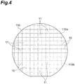
- the wafer 110 is a wafer including parts corresponding to a plurality of substrates 1 1 arranged in a two-dimensional state and being expected to be cut into the plurality of substrates 11 along each of a plurality of lines 10.
- the wafer 110 has a first main surface 110a and a second main surface 110b facing each other.
- the wafer 110 is made of silicon, quartz, or glass.
- each of the substrates 11 exhibits a rectangular shape in a case of being seen in a direction perpendicular to the first main surface 110a
- the plurality of substrates 11 are arranged in a two-dimensional matrix state, and the plurality of lines 10 are set in a lattice state to pass through a location between the substrates 11 adjacent to each other.
- a forming step is carried out.
- a reflection prevention layer 210, a first mirror layer 220, a sacrificial layer 230, a second mirror layer 240, and a first thinned region 290 are formed on the first main surface 110a of the wafer 110 (refer to FIG. 7(a) ).
- a stress adjustment layer 400, a light shielding layer 450, a protective layer 460, and a second thinned region 470 are formed on the second main surface 110b of the wafer 110 (refer to FIG. 7(a) ).
- the reflection prevention layer 210 is formed on the first main surface 110a of the wafer 110, and a reflection prevention layer 410 is formed on the second main surface 110b of the wafer 110.
- the reflection prevention layer 210 is a layer expected to be cut into a plurality of reflection prevention layers 21 along each of the lines 10.
- the reflection prevention layer 410 is a layer expected to be cut into a plurality of reflection prevention layers 41 along each of the lines 10.
- the first mirror layer 220 is a layer having a plurality of first mirror portions 31 each of which is expected to function as a fixed mirror and is a layer expected to be cut into a plurality of first laminates 22 along each of the lines 10.
- the layer 420 configuring the stress adjustment layer 400 is a layer expected to be cut into a plurality of third laminates 42 along each of the lines 10.
- the first mirror layer 220 When the first mirror layer 220 is formed, a part along each of the lines 10 in the first mirror layer 220 is removed through etching, such that the surface of the reflection prevention layer 210 is exposed.
- a predetermined polysilicon layer in the first mirror layer 220 is partially decreased in resistance by doping impurities, so that the first electrode 12, the second electrode 13, and the wirings 12a and 13a are formed in each part corresponding to the substrate 11.
- the trenches 17 and 18 are formed on the surface of the first mirror layer 220 in each part corresponding to the substrate 11 through etching.
- the sacrificial layer 230 is formed on the first mirror layer 220 and the exposed surface of the reflection prevention layer 210, and a layer 430 configuring the stress adjustment layer 400 is formed on the layer 420 configuring the stress adjustment layer 400.
- the sacrificial layer 230 is a layer having a plurality of portions 50 expected to be removed and is a layer expected to be cut into a plurality of intermediate layers 23 along each of the lines 10.
- the portion 50 expected to be removed is a part corresponding to the gap S (refer to FIG. 3 ).
- the layer 430 configuring the stress adjustment layer 400 is a layer expected to be cut into a plurality of intermediate layers 43 along each of the lines 10.
- a part along each of the lines 10 in the sacrificial layer 230 and the reflection prevention layer 210 is removed through etching, such that the first main surface 110a of the wafer 110 is exposed.
- a gap is formed in a part corresponding to each of the terminals 15 and 16 (refer to FIG. 3 ) in the sacrificial layer 230.
- a plurality of polysilicon layers and a plurality of silicon nitride layers are alternately laminated on each of the first main surface 110a side and the second main surface 110b side of the wafer 110, so that the second mirror layer 240 is formed on the sacrificial layer 230 and the exposed first main surface 110a of the wafer 110, and a layer 440 configuring the stress adjustment layer 400 is formed on the layer 430 configuring the stress adjustment layer 400.
- the second mirror layer 240 is a layer having a plurality of second mirror portions 32 each of which is expected to function as a movable mirror and is a layer expected to be cut into a plurality of second laminates 24 along each of the lines 10.
- the layer 440 configuring the stress adjustment layer 400 is a layer expected to be cut into a plurality of fourth laminates 44 along each of the lines 10.
- the second mirror layer 240 When the second mirror layer 240 is formed, side surfaces 230a of the sacrificial layer 230, side surfaces 220a of the first mirror layer 220, and side surface 210a of the reflection prevention layer 210, facing each other along the line 10 are covered with the second mirror layer 240.
- a predetermined polysilicon layer in the second mirror layer 240 is partially decreased in resistance by doping impurities, so that the third electrode 14 and the wiring 14a are formed in each part corresponding to the substrate 11.
- a part along each of the lines 10 in the second mirror layer 240 is thinned, such that the surface of the polysilicon layer 27a configuring the second mirror layer 240 (refer to FIG. 3 ) (that is, the polysilicon layer positioned closest to the first main surface 110a side) is exposed (more specifically, such that the surface of the polysilicon layer 27a is exposed in a case of being seen in a direction perpendicular to the first main surface 110a).
- a gap is formed in a part corresponding to each of the terminals 15 and 16 (refer to FIG. 3 ) in the second mirror layer 240.
- the terminals 15 and 16 are formed in the gap, the terminal 15 and the wiring 12a are connected to each other, and the terminal 16 and each of the wiring 13a and the wiring 14a are connected to each other.
- the reflection prevention layer 210, the first mirror layer 220, the sacrificial layer 230, the second mirror layer 240, and the first thinned region 290 are formed on the first main surface 110a of the wafer 110.
- the first thinned region 290 is a region in which the first mirror layer 220, the sacrificial layer 230, and the second mirror layer 240 are partially thinned along each of the lines 10.
- the reflection prevention layer 210, the first mirror layer 220, the sacrificial layer 230, and the second mirror layer 240 are formed such that one reflection prevention layer 21, one first mirror portion 31, one portion 50 expected to be removed, and one second mirror portion 32 are disposed from one substrate 11 side in this order (that is, in order of one reflection prevention layer 21, one first mirror portion 31, one portion 50 expected to be removed, and one second mirror portion 32).
- the plurality of through-holes 24b leading from the surface 24a of the second laminate 24 to the portion 50 expected to be removed are formed in the second laminate 24 through etching.
- the light shielding layer 450 is formed on the layer 440 configuring the stress adjustment layer 400.
- the light shielding layer 450 is a layer expected to be cut into a plurality of light shielding layers 45 along each of the lines 10.
- a part along each of the lines 10 in the light shielding layer 450 and the stress adjustment layer 400 is removed through etching, such that the surface of the reflection prevention layer 410 is exposed.
- the opening 40a is formed in each part corresponding to the substrate 11 through the etching.
- the protective layer 460 is formed on the light shielding layer 450, the exposed surface of the reflection prevention layer 410, an inner surface of the opening 40a, and the side surface of the stress adjustment layer 400 facing the second thinned region 470.
- the protective layer 460 is a layer expected to be cut into a plurality of protective layers 46 along each of the lines 10.
- the stress adjustment layer 400, the light shielding layer 450, the protective layer 460, and the second thinned region 470 are formed on the second main surface 110b of the wafer 110.
- the second thinned region 470 is a region in which the stress adjustment layer 400 is partially thinned along each of the lines 10.
- a removing step is carried out. Specifically, the plurality of portions 50 expected to be removed are removed all at the same time from the sacrificial layer 230 through etching (for example, gas phase etching using hydrofluoric acid gas) through the plurality of through-holes 24b. Accordingly, the gap S is formed in each part corresponding to the substrate 11.
- etching for example, gas phase etching using hydrofluoric acid gas
- a cutting step is carried out. Specifically, as illustrated in FIG. 8(a) , an expanding tape 60 is attached onto the protective layer 460 (that is, to the stress adjustment layer 400 side). Subsequently, in a state in which the expanding tape 60 is attached to the stress adjustment layer 400 side, irradiation of a laser light L is performed from a side opposite to the expanding tape 60, and a converging point of the laser light L is relatively moved along each of the lines 10 while the converging point of the laser light L is positioned within the wafer 110. That is, the laser light L is incident on the wafer 110 from a side opposite to the expanding tape 60 through the surface of the polysilicon layer exposed in the first thinned region 290.
- a modified region is formed within the wafer 110 along each of the lines 10 through the irradiation of the laser light L.
- the modified region indicates a region in which a density, a refractive index, mechanical strength, and other physical characteristics have attained states different from those on the surroundings and indicates a region which becomes a start point of a crack extended in a thickness direction of the wafer 110.
- Examples of the modified region include molten processed regions (which means at least any one of a region resolidified after melting, a region in a melted state, and a region in the state of being resolidified from the melted state), a crack region, a dielectric breakdown region, a refractive index changed region, and a mixed region thereof.
- the modified region there are a region where the density of the modified region has changed from that of an unmodified region and a region formed with a lattice defect in a material of the wafer 110 as the modified region.
- the material of the wafer 110 is monocrystalline silicon
- the modified region can also be referred to as a high dislocation density region.
- the number of rows of the modified regions arranged in the thickness direction of the wafer 110 with respect to each of the lines 10 is appropriately adjusted based on the thickness of the wafer 110.
- the expanding tape 60 attached to the stress adjustment layer 400 side is expanded, so that a crack is extended in the thickness direction of the wafer 110 from the modified region formed within the wafer 110, and the wafer 110 is then cut into the plurality of substrates 11 along each of the lines 10.
- the polysilicon layer of the second mirror layer 240 is cut along each of the lines 10 in the first thinned region 290, and the reflection prevention layer 410 and the protective layer 460 are cut along each of the lines 10 in the second thinned region 470. Accordingly, a plurality of Fabry-Perot interference filters 1 in a state of being separated from each other on the expanding tape 60 are obtained.
- the modified region is formed within the wafer 110 along each of the lines 10 through irradiation of the laser light L. Accordingly, scattering or the like of the laser light L is prevented so that the modified region can be reliably formed within the wafer 110.
- the Fabry-Perot interference filter 1 since at least one of the first mirror layer 220, the sacrificial layer 230, and the second mirror layer 240 is partially thinned along each of the lines 10, it is possible to prevent damage from being caused in the first mirror layer 220, the sacrificial layer 230, and the second mirror layer 240 when the wafer 110 is cut into the plurality of substrates 11 along each of the lines 10 (if the first thinned region 290 is not formed, an impact, stress, or the like is transferred to the first mirror layer 220, the sacrificial layer 230, and the second mirror layer 240 so that damage is likely to be caused when the wafer 110 is cut into the plurality of substrates 11 along each of the lines 10).
- both manufacturing efficiency and a yield can be improved, and the Fabry-Perot interference filter 1 with high quality can be stably mass-produced.
- the stress adjustment layer 400 is formed on the second main surface 110b of the wafer 110, and the second thinned region 470 in which the stress adjustment layer 400 is partially thinned along each of the lines 10 is formed. Accordingly, it is possible to prevent warping of the wafer 110 caused by discordance of the layer configuration between the first main surface 110a side and the second main surface 110b side.
- the stress adjustment layer 400 is partially thinned along each of the lines 10, it is possible to prevent damage from being caused in the stress adjustment layer 400 such as a part on the periphery of the opening 40a when the wafer 110 is cut into the plurality of substrates 11 along each of the lines 10, (if the second thinned region 470 is not formed, an impact, stress, or the like is transferred to the stress adjustment layer 400 such as a part on the periphery of the opening 40a so that damage is likely to be caused when the wafer 110 is cut into the plurality of substrates 11 along each of the lines 10).
- the Fabry-Perot interference filter 1 since the first mirror layer 220, the sacrificial layer 230, and the second mirror layer 240 formed on the first main surface 110a of the wafer 110, and the stress adjustment layer 400 formed on the second main surface 110b of the wafer 110 are thin and elaborate layer structures, if the first thinned region 290 and the second thinned region 470 are not formed before the cutting step is carried out, damage is likely to be caused in the layer structure in the cutting step. This becomes noticeable because a force acts such that the layer structure is torn off when carrying out the cutting step in which the crack is extended from the modified region by expanding the expanding tape 60.
- the first thinned region 290 and the second thinned region 470 are formed before the cutting step is carried out, so that it is possible to carry out laser processing with less contamination during a dry process (internal processing-type laser processing for forming a modified region within the wafer 110) while damage is prevented from being caused in the layer structure.
- each of the first mirror layer 220, the sacrificial layer 230, the second mirror layer 240, and the stress adjustment layer 400 has a thin layer structure, it is difficult to stably form a modified region leading to the within of the layers thereof through irradiation of the laser light L" and "in contrast, since each of the first mirror layer 220, the sacrificial layer 230, the second mirror layer 240, and the stress adjustment layer 400 has a thin layer structure, the layers are likely to be torn off and be greatly damaged unless the first thinned region 290 and the second thinned region 470 are formed".
- the forming step is carried out to form the first mirror layer 220, the sacrificial layer 230, the second mirror layer 240, and the first thinned region 290 on the first main surface 110a of the wafer 110 and to form the stress adjustment layer 400 and the second thinned region 470 on the second main surface 110b of the wafer 110.
- the removing step is carried out to remove the portion 50 expected to be removed from the sacrificial layer 230. Accordingly, the removing step is carried out in a state in which internal stress of the wafer 110 is reduced.
- the crack is extended in the thickness direction of the wafer 110 from the modified region by expanding the expanding tape 60 attached to the stress adjustment layer 400 side. Accordingly, it is possible to prevent damage from being caused due to the attached expanding tape 60 in the second mirror layer 240 having the plurality of second mirror portions 32 each of which is expected to function as the movable mirror. Moreover, since an expanding force of the expanding tape 60 is likely to be concentrated in the modified region and a part in the vicinity thereof due to the presence of the second thinned region 470, the crack can be easily extended in the thickness direction of the wafer 110 from the modified region.
- the laser light L is incident on the wafer 110 from a side opposite to the expanding tape 60. Accordingly, scattering, attenuation, or the like of the laser light L caused by the expanding tape 60 is prevented so that the modified region can be reliably formed within the wafer 110 along each of the lines 10.
- the removing step of removing the portion 50 expected to be removed from the sacrificial layer 230 through etching is carried out before the cutting step (that is, between the forming step and the cutting step) of cutting the wafer 110 into the plurality of substrates 11 along each of the lines 10. Accordingly, since the removing step of removing the portion 50 expected to be removed from the sacrificial layer 230 through etching is carried out at wafer 110 level, compared to a case in which the removing step is individually carried out at chip level, it is possible to form the gap S between the first mirror portion 31 and the second mirror portion 32 in a remarkably efficient way.
- the side surfaces 230a of the sacrificial layer 230 facing each other along each of the lines 10 are covered with the second mirror layer 240 by forming the second mirror layer 240 on the sacrificial layer 230. Accordingly, it is possible to prevent a part of the side surfaces 230a of the sacrificial layer 230 from being removed (erosion) when the portion 50 expected to be removed is removed from the sacrificial layer 230 through etching. Moreover, in the manufactured Fabry-Perot interference filter 1, it is possible to prevent light which becomes stray light from being incident from the side surface 23b of the intermediate layer 23 corresponding to the side surface 230a of the sacrificial layer 230.
- a part along each of the lines 10 in at least one of the first mirror layer 220, the sacrificial layer 230, and the second mirror layer 240 is thinned such that the surface of the polysilicon layer configuring the second mirror layer 240 is exposed (more specifically, such that the surface of the polysilicon layer 27a is exposed in a case of being seen in a direction perpendicular to the first main surface 110a).
- the laser light L is incident on the wafer 110 through the surface of the polysilicon layer included in the second mirror layer 240.
- the first main surface 110a of the wafer 110 is protected by the polysilicon layer of which the surface is exposed, and flatness of a surface, on which the laser light L is incident, is maintained. Therefore, scattering or the like of the laser light L is prevented so that the modified region can be more reliably formed within the wafer 110.
- the removing step of removing the portion 50 expected to be removed from the sacrificial layer 230 through etching is carried out after the cutting step of cutting the wafer 110 into the plurality of substrates 11 along each of the lines 10.
- the reason is that, for example, if forming of the gap S in the sacrificial layer 230 is carried out before blade dicing, there is increasing concern that the second mirror portion 32 floating in the gap S is damaged when blade dicing is carried out. In addition, there is increasing concern that particles generated when blade dicing is carried out infiltrate into the gap S or cooling rinse water used in blade dicing infiltrates into the gap S.
- the method of manufacturing a Fabry-Perot interference filter of the present disclosure is not limited to the embodiment described above.
- the material and the shape of each configuration are not limited to the material and the shape described above, and it is possible to employ various materials and shapes.
- the order of forming each layer and each region in the forming step is not limited to that described above.
- the first thinned region 290 may be formed by forming the first mirror layer 220, the sacrificial layer 230, and the second mirror layer 240 on the first main surface 110a of the wafer 110, and then thinning a part along each of the lines 10 in the first mirror layer 220, the sacrificial layer 230, and the second mirror layer 240.
- first thinned region 290 and the second thinned region 470 may be formed after forming the first mirror layer 220, the sacrificial layer 230, and the second mirror layer 240 on the first main surface 110a of the wafer 110, and forming the stress adjustment layer 400 on the second main surface 110b of the wafer 110.
- the first thinned region 290 need only be a region in which at least one of the first mirror layer 220, the sacrificial layer 230, and the second mirror layer 240 is partially thinned along each of the lines 10. Therefore, the first thinned region 290 may be a region from which all of the parts along each of the lines 10 in all of the layers on the first main surface 110a side including the first mirror layer 220, the sacrificial layer 230, and the second mirror layer 240 are removed.
- the second thinned region 470 need only be a region in which at least a part of the stress adjustment layer 400 is partially thinned along each of the lines 10. Therefore, the second thinned region 470 may be a region from which all of the parts along each of the lines 10 in all of the layers on the second main surface 110b side including the stress adjustment layer 400 are removed. In the forming step, the second thinned region 470 does not have to be formed. Moreover, the stress adjustment layer 400 itself does not have to be formed.
- the removing step of removing the portion 50 expected to be removed from the sacrificial layer 230 through etching may be carried out after the cutting step of cutting the wafer 110 into the plurality of substrates 11 along each of the lines 10. In this case, in each part corresponding to the substrate 11, the portion 50 expected to be removed is removed from the sacrificial layer 230 through etching.
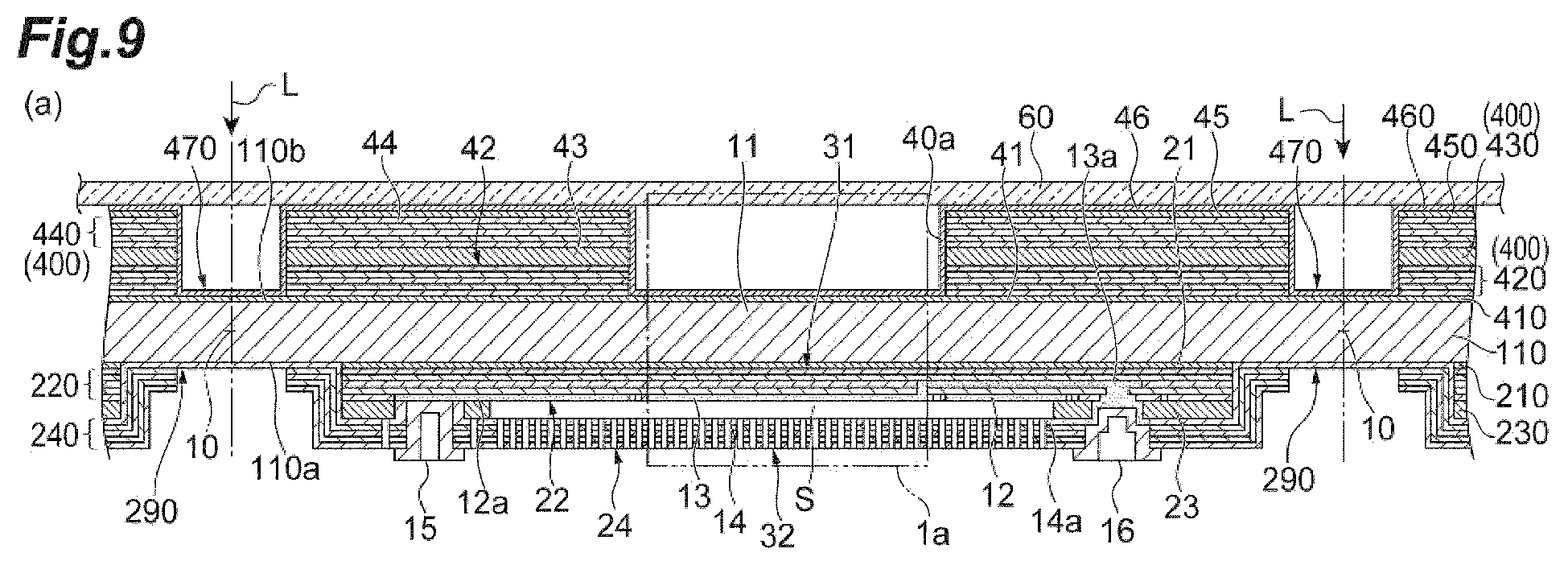
- the cutting step may be carried out as illustrated in FIGS. 9(a) and 9(b) .
- the expanding tape 60 is attached onto the protective layer 460 (that is, the stress adjustment layer 400 side).
- irradiation of the laser light L is performed from the expanding tape 60 side, and the converging point of the laser light L is relatively moved along each of the lines 10 while the converging point of the laser light L is positioned within the wafer 110. That is, the laser light L is incident on the wafer 110 from the expanding tape 60 side through the expanding tape 60.
- the modified region is formed within the wafer 110 along each of the lines 10 through the irradiation of the laser light L.
- crack is extended in the thickness direction of the wafer 1 10 from the modified region formed within the wafer 110 by expanding the expanding tape 60 attached to the stress adjustment layer 400 side, and the wafer 110 is cut into the plurality of substrates 11 along each of the lines 10. Then, the plurality of Fabry-Perot interference filters 1 in a state of being separated from each other on the expanding tape 60 are obtained.
- the expanding tape 60 functions as a cover. Therefore, it is possible to prevent such particles from adhering to the second mirror layer 240 or the like.
- the cutting step when the modified region is formed within the wafer 110 along each of the lines 10 through irradiation of the laser light L, crack may be extended in the thickness direction of the wafer 110 from the modified region and the wafer 110 may be cut into the plurality of substrates 11 along each of the lines 10.
- the plurality of Fabry-Perot interference filters 1 obtained through cutting can be separated from each other by expanding the expanding tape 60.
- At least one of the first mirror layer 220, the sacrificial layer 230, and the second mirror layer 240 may be partially thinned along each of the lines 10 such that the surface of the polysilicon layer configuring the first mirror layer 220 instead of the second mirror layer 240 is exposed, and in the cutting step, the laser light L may be incident on the wafer 110 through the surface of the polysilicon layer included in the first mirror layer 220 instead of the second mirror layer 240.
- the layer of which the surface is exposed in the forming step need only be at least one layer configuring the first mirror layer 220 or the second mirror layer 240.
- the layer of which the surface is exposed in the forming step is not limited to a polysilicon layer and may be a silicon nitride layer or a silicon oxide layer, for example.
- the first main surface 110a of the wafer 110 is protected by the layer of which the surface is exposed, and flatness of a surface, on which the laser light L is incident, is maintained. Therefore, scattering or the like of the laser light L is prevented so that the modified region can be more reliably formed within the wafer 110.
- Fabry-Perot interference filter 10: line, 11: substrate, 31: first mirror portion, 32: second mirror portion, 50: portion expected to be removed, 60: expanding tape, 110: wafer, 110a: first main surface, 110b: second main surface, 220: first mirror layer, 230: sacrificial layer, 230a: side surface, 240: second mirror layer, 290: first thinned region, 400: stress adjustment layer, 470: second thinned region, L: laser light
Landscapes
- Physics & Mathematics (AREA)
- Engineering & Computer Science (AREA)
- Optics & Photonics (AREA)
- Spectroscopy & Molecular Physics (AREA)
- General Physics & Mathematics (AREA)
- Mechanical Engineering (AREA)
- Plasma & Fusion (AREA)
- Microelectronics & Electronic Packaging (AREA)
- Manufacturing & Machinery (AREA)
- Computer Hardware Design (AREA)
- Chemical Kinetics & Catalysis (AREA)
- General Chemical & Material Sciences (AREA)
- Oil, Petroleum & Natural Gas (AREA)
- Chemical & Material Sciences (AREA)
- Mechanical Light Control Or Optical Switches (AREA)
- Micromachines (AREA)
- Optical Filters (AREA)
Abstract
Description
- The present disclosure relates to a method of manufacturing a Fabry-Perot interference filter.
- In the related art, a Fabry-Perot interference filter, which includes a substrate, a fixed mirror and a movable mirror facing each other with a gap interposed therebetween on the substrate, and an intermediate layer defining the gap, is known (for example, refer to Patent Literature 1).
- Patent Literature 1: Japanese Unexamined Patent Publication No.
2013-506154 - Since a Fabry-Perot interference filter as described above is a fine structure, it is difficult to improve both manufacturing efficiency and a yield when a Fabry-Perot interference filter is manufactured.
- Accordingly, an object of the present disclosure is to provide a method of manufacturing a Fabry-Perot interference filter, in which both manufacturing efficiency and a yield can be improved.
- According to an aspect of the present disclosure, there is provided a method of manufacturing a Fabry-Perot interference filter including a forming step of forming a first thinned region in the forming step, a first mirror layer having a plurality of first mirror portions each of which is expected to function as a fixed mirror, a sacrificial layer having a plurality of portions expected to be removed, and a second mirror layer having a plurality of second mirror portions each of which is expected to function as a movable mirror are formed on a first main surface of a wafer expected to be cut into a plurality of substrates along each of a plurality of lines such that one first mirror portion, one portion expected to be removed, and one second mirror portion are disposed in this order from one substrate side, and the first thinned region in which at least one of the first mirror layer, the sacrificial layer, and the second mirror layer is partially thinned along each of the plurality of lines is formed; a cutting step of cutting the wafer into the plurality of substrates along each of the plurality of lines by forming a modified region within the wafer along each of the plurality of lines through irradiation of a laser light and extending a crack in a thickness direction of the wafer from the modified region, after the forming step; and a removing step of removing the portion expected to be removed from the sacrificial layer through etching, between the forming step and the cutting step or after the cutting step.
- In the method of manufacturing a Fabry-Perot interference filter, after forming the first thinned region in which at least one of the first mirror layer, the sacrificial layer, and the second mirror layer is partially thinned along each of the lines, the modified region is formed within the wafer along each of the lines through irradiation of a laser light. Accordingly, scattering or the like of a laser light is prevented so that the modified region can be reliably formed within the wafer. Moreover, since at least one of the first mirror layer, the sacrificial layer, and the second mirror layer is partially thinned along each of the lines, it is possible to prevent damage from being caused in the first mirror layer, the sacrificial layer, and the second mirror layer when a wafer is cut into a plurality of substrates along each of the lines. Thus, according to the method of manufacturing a Fabry-Perot interference filter, both manufacturing efficiency and a yield can be improved. The "first thinned region" includes a region from which all of the parts along each of the lines in the first mirror layer, the sacrificial layer, and the second mirror layer are removed.
- According to the aspect of the present disclosure, in the method of manufacturing a Fabry-Perot interference filter, in the forming step, a stress adjustment layer may be formed on a second main surface of the wafer, and a second thinned region in which the stress adjustment layer is partially thinned along each of the plurality of lines may be formed. According to this configuration, it is possible to prevent warping of the wafer caused by discordance of a layer configuration between the first main surface side and the second main surface side. Moreover, since the stress adjustment layer is partially thinned along each of the lines, it is possible to prevent damage from being caused in the stress adjustment layer when a wafer is cut into a plurality of substrates along each of the lines. The "second thinned region" includes a region from which all of the parts along each of the lines in the stress adjustment layer are removed.
- According to the aspect of the present disclosure, in the method of manufacturing a Fabry-Perot interference filter, in the cutting step, the crack may be extended in the thickness direction of the wafer from the modified region by expanding an expanding tape attached to the stress adjustment layer side. According to this configuration, it is possible to prevent damage from being caused due to the attached expanding tape in the second mirror layer having the plurality of second mirror portions each of which is expected to function as the movable mirror. Moreover, since an expanding force of the expanding tape is likely to be concentrated in the modified region and a part in the vicinity thereof due to the presence of the second thinned region, the crack can be easily extended in the thickness direction of the wafer from the modified region.
- According to the aspect of the present disclosure, in the method of manufacturing a Fabry-Perot interference filter, in the cutting step, in a state in which the expanding tape is attached to the stress adjustment layer side, the laser light may be incident on the wafer from a side opposite to the expanding tape. According to this configuration, scattering, attenuation, or the like of a laser light caused by the expanding tape is prevented so that the modified region can be reliably formed within the wafer along each of the lines.
- According to the aspect of the present disclosure, in the method of manufacturing a Fabry-Perot interference filter, in the cutting step, in a state in which the expanding tape is attached to the stress adjustment layer side, the laser light may be incident on the wafer through the expanding tape from the expanding tape side. According to this configuration, for example, even if particles fall due to their own weight when irradiation of a laser light is performed from above, the expanding tape functions as a cover. Therefore, it is possible to prevent such particles from adhering to the second mirror layer or the like.
- According to the aspect of the present disclosure, in the method of manufacturing a Fabry-Perot interference filter, the removing step may be carried out between the forming step and the cutting step. According to this configuration, since the removing step of removing the portion expected to be removed from the sacrificial layer through etching is carried out at wafer level, compared to a case in which the removing step is individually carried out at chip level, it is possible to form a gap between the first mirror portion and the second mirror portion in a remarkably efficient way. At this time, although parts respectively corresponding to the plurality of second mirror portions in the second mirror layer are in a state of floating in the gap, the following cutting step is carried out through irradiation of a laser light. Therefore, it is possible to effectively prevent a situation in which the second mirror portions floating in the gap become damaged.
- According to the aspect of the present disclosure, in the method of manufacturing a Fabry-Perot interference filter, in the forming step, after a part along each of the plurality of lines in the sacrificial layer formed on the first mirror layer is thinned, side surfaces of the sacrificial layer facing each other along each of the plurality of lines may be covered with the second mirror layer by forming the second mirror layer on the sacrificial layer. According to this configuration, it is possible to prevent a part of the side surfaces of the sacrificial layer from being removed when the portion expected to be removed is removed from the sacrificial layer through etching. Moreover, in a manufactured Fabry-Perot interference filter, it is possible to prevent light which becomes stray light from being incident from the side surface of an intermediate layer corresponding to the side surface of the sacrificial layer.
- According to the aspect of the present disclosure, in the method of manufacturing a Fabry-Perot interference filter, in the forming step, a part along each of the plurality of lines in at least one of the first mirror layer, the sacrificial layer, and the second mirror layer may be thinned such that a surface of at least one layer configuring the first mirror layer or the second mirror layer is exposed. In the cutting step, the laser light may be incident on the wafer through the surface of the layer. According to this configuration, the first main surface of the wafer is protected by at least one layer configuring the first mirror layer or the second mirror layer, and flatness of a surface, on which a laser light is incident, is maintained. Therefore, scattering or the like of a laser light is prevented so that the modified region can be more reliably formed within the wafer.
- According to the present disclosure, it is possible to provide a method of manufacturing a Fabry-Perot interference filter, in which both manufacturing efficiency and a yield can be improved.
-
-
FIG. 1 is a plan view of a Fabry-Perot interference filter of an embodiment. -
FIG. 2 is a bottom view of the Fabry-Perot interference filter inFIG. 1 . -
FIG. 3 is a cross-sectional view of the Fabry-Perot interference filter taken along line III-III inFIG. 1 . -
FIG. 4 is a plan view of a wafer used in a method of manufacturing the Fabry-Perot interference filter inFIG. 1 . -
FIGS. 5(a) and 5(b) are cross-sectional views for describing the method of manufacturing the Fabry-Perot interference filter inFIG. 1 . -
FIGS. 6(a) and 6(b) are cross-sectional views for describing the method of manufacturing the Fabry-Perot interference filter inFIG. 1 . -
FIGS. 7(a) and 7(b) are cross-sectional views for describing the method of manufacturing the Fabry-Perot interference filter inFIG. 1 . -
FIGS. 8(a) and 8(b) are cross-sectional views for describing the method of manufacturing the Fabry-Perot interference filter inFIG. 1 . -
FIGS. 9(a) and 9(b) are cross-sectional views for describing the method of manufacturing the Fabry-Perot interference filter inFIG. 1 . - Hereinafter, an embodiment of the present disclosure will be described in detail with reference to the drawings. In all the drawings, the same or equivalent portions are denoted with the same reference numerals and duplicated description is omitted.
- As illustrated in
FIGS. 1 ,2 , and3 , a Fabry-Perot interference filter 1 includes asubstrate 11. Thesubstrate 11 has afirst surface 11a and asecond surface 11b facing thefirst surface 11a. On thefirst surface 11a, areflection prevention layer 21, a first laminate (first layer) 22, anintermediate layer 23, and a second laminate (second layer) 24 are laminated in this order. A gap (air gap) S is defined between thefirst laminate 22 and thesecond laminate 24 by the frame-shapedintermediate layer 23. - The shape and the positional relationship of each portion in a case of being seen in a direction perpendicular to the
first surface 11a (plan view) are as follows. For example, an outer edge of thesubstrate 11 has a rectangular shape. The outer edge of thesubstrate 11 and an outer edge of thesecond laminate 24 coincide with each other. An outer edge of thereflection prevention layer 21, an outer edge of thefirst laminate 22, and an outer edge of theintermediate layer 23 coincide with each other. Thesubstrate 11 has anouter edge portion 11c positioned on an outer side of the outer edge of theintermediate layer 23 with respect to the center of the gap S. For example, theouter edge portion 11c has a frame shape and surrounds theintermediate layer 23 in a case of being seen in a direction perpendicular to thefirst surface 11a. - In the Fabry-
Perot interference filter 1, light having a predetermined wavelength is transmitted through alight transmission region 1a defined in a center portion thereof. For example, thelight transmission region 1a is a columnar region. For example, thesubstrate 11 is made of silicon, quartz, or glass. When thesubstrate 11 is made of silicon, thereflection prevention layer 21 and theintermediate layer 23 are made of silicon oxide, for example. The thickness of theintermediate layer 23 ranges from several tens of nm to several tens of µm, for example. - A part corresponding to the
light transmission region 1a in thefirst laminate 22 functions as afirst mirror portion 31. Thefirst mirror portion 31 is disposed on thefirst surface 11a with thereflection prevention layer 21 interposed therebetween. Thefirst laminate 22 is configured to have a plurality ofpolysilicon layers 25 and a plurality of silicon nitride layers 26 which are alternately laminated one by one. In the present embodiment, a polysilicon layer 25a, asilicon nitride layer 26a, apolysilicon layer 25b, asilicon nitride layer 26b, and apolysilicon layer 25c are laminated on thereflection prevention layer 21 in this order. The optical thickness of each of thepolysilicon layer 25 and thesilicon nitride layer 26 configuring thefirst mirror portion 31 is preferably an integral multiple of 1/4 of a center transmission wavelength. Thefirst mirror portion 31 may be directly disposed on thefirst surface 11a without thereflection prevention layer 21 interposed therebetween. - A part corresponding to the
light transmission region 1a in thesecond laminate 24 functions as asecond mirror portion 32. Thesecond mirror portion 32 faces thefirst mirror portion 31 with the gap S interposed therebetween on a side opposite to thesubstrate 11 with respect to thefirst mirror portion 31. Thesecond laminate 24 is disposed on thefirst surface 11a with thereflection prevention layer 21, thefirst laminate 22, and theintermediate layer 23 interposed therebetween. Thesecond laminate 24 is configured to include a plurality ofpolysilicon layers 27 and a plurality of silicon nitride layers 28 which are alternately laminated one by one. In the present embodiment, apolysilicon layer 27a, asilicon nitride layer 28a, apolysilicon layer 27b, asilicon nitride layer 28b, and apolysilicon layer 27c are laminated on theintermediate layer 23 in this order. The optical thickness of each of thepolysilicon layer 27 and thesilicon nitride layer 28 configuring thesecond mirror portion 32 is preferably an integral multiple of 1/4 of the center transmission wavelength. - In the
first laminate 22 and thesecond laminate 24, silicon oxide layers may be used in place of the silicon nitride layers. In addition, as the material of each layer configuring thefirst laminate 22 and thesecond laminate 24, titanium oxide, tantalum oxide, zirconium oxide, magnesium fluoride, aluminum oxide, calcium fluoride, silicon, germanium, zinc sulfide, or the like may be used. - In a part corresponding to the gap S in the
second laminate 24, a plurality of through-holes 24b leading from asurface 24a of thesecond laminate 24 on a side opposite to theintermediate layer 23 to the gap S are formed. The plurality of through-holes 24b are formed so as not to substantially affect the function of thesecond mirror portion 32. The plurality of through-holes 24b are used for forming the gap S by removing a part of theintermediate layer 23 through etching. - In addition to the
second mirror portion 32, thesecond laminate 24 further has a coveringportion 33 and aperipheral edge portion 34. Thesecond mirror portion 32, the coveringportion 33, and theperipheral edge portion 34 are integrally formed to have a part of the same laminated structure as each other and to be connected to each other. The coveringportion 33 surrounds thesecond mirror portion 32 in a case of being seen in a direction perpendicular to thefirst surface 11a. The coveringportion 33 covers asurface 23a of theintermediate layer 23 on a side opposite to thesubstrate 11, aside surface 23b of the intermediate layer 23 (a side surface on the outer side, that is, a side surface on a side opposite to the gap S side), aside surface 22a of thefirst laminate 22, and aside surface 21a of thereflection prevention layer 21 and leads to thefirst surface 11a. That is, the coveringportion 33 covers the outer edge of theintermediate layer 23, the outer edge of thefirst laminate 22, and the outer edge of thereflection prevention layer 21. - The
peripheral edge portion 34 surrounds the coveringportion 33 in a case of being seen in a direction perpendicular to thefirst surface 11a. Theperipheral edge portion 34 is positioned on thefirst surface 11a in theouter edge portion 11c. An outer edge of theperipheral edge portion 34 coincides with the outer edge of thesubstrate 11 in a case of being seen in a direction perpendicular to thefirst surface 11a. - The
peripheral edge portion 34 is thinned along an outer edge of theouter edge portion 11c. That is, a part along the outer edge of theouter edge portion 11c in theperipheral edge portion 34 is thinned compared to other parts excluding the part along the outer edge in theperipheral edge portion 34. In the present embodiment, theperipheral edge portion 34 is thinned by removing a part of thepolysilicon layer 27 and thesilicon nitride layer 28 configuring thesecond laminate 24. Theperipheral edge portion 34 has anon-thinned portion 34a connected to the coveringportion 33, and a thinnedportion 34b surrounding thenon-thinned portion 34a. In the thinnedportion 34b, thepolysilicon layer 27 and thesilicon nitride layer 28 excluding thepolysilicon layer 27a directly provided on thefirst surface 11a are removed. - The height of a
surface 34c of thenon-thinned portion 34a on a side opposite to thesubstrate 1 1 from thefirst surface 11a is lower than the height of thesurface 23a of theintermediate layer 23 from thefirst surface 11a. The height of thesurface 34c of thenon-thinned portion 34a from thefirst surface 11a ranges from 100 nm to 5,000 nm, for example. The height of thesurface 23a of theintermediate layer 23 from thefirst surface 11a is a height greater than the height of thesurface 34c of thenon-thinned portion 34a from thefirst surface 11a within a range from 500 nm to 20,000 nm, for example. The width of the thinnedportion 34b (distance between an outer edge of thenon-thinned portion 34a and the outer edge of theouter edge portion 11c) is equal to or greater than 0.01 times the thickness of thesubstrate 11. The width of the thinnedportion 34b ranges from 5 µm to 400 µm, for example. The thickness of thesubstrate 11 ranges from 500 µm to 800 µm, for example. - A
first electrode 12 is formed in thefirst mirror portion 31 such that thelight transmission region 1a is surrounded. Thefirst electrode 12 is formed by doping impurities into thepolysilicon layer 25c and decreasing resistance. Asecond electrode 13 is formed in thefirst mirror portion 31 such that thelight transmission region 1a is included. Thesecond electrode 13 is formed by doping impurities into thepolysilicon layer 25c and decreasing resistance. The size of thesecond electrode 13 is preferably a size for including the entirety of thelight transmission region 1a. However, the size may be approximately the same as the size of thelight transmission region 1a. - A
third electrode 14 is formed in thesecond mirror portion 32. Thethird electrode 14 faces thefirst electrode 12 and thesecond electrode 13 with the gap S interposed therebetween. Thethird electrode 14 is formed by doping impurities into thepolysilicon layer 27a and decreasing resistance. - A pair of
terminals 15 is provided to face each other while having thelight transmission region 1a therebetween. Each of theterminals 15 is disposed inside a through-hole leading from thesurface 24a of thesecond laminate 24 to thefirst laminate 22. Each of theterminals 15 is electrically connected to thefirst electrode 12 via awiring 12a. For example, theterminals 15 are formed from a metal film made of aluminum or an alloy thereof. - A pair of
terminals 16 is provided to face each other while having thelight transmission region 1a therebetween. Each of theterminals 16 is disposed inside a through-hole leading from thesurface 24a of thesecond laminate 24 to thefirst laminate 22. Each of theterminals 16 is electrically connected to thesecond electrode 13 via awiring 13a and is electrically connected to thethird electrode 14 via awiring 14a. For example, theterminals 16 are formed from a metal film made of aluminum or an alloy thereof. The facing direction of the pair ofterminals 15 and the facing direction of the pair ofterminals 16 are orthogonal to each other (refer toFIG. 1 ). -
Trenches surface 22b of thefirst laminate 22. Thetrench 17 annularly extends to surround a connection part with respect to theterminals 16 in thewiring 13a. Thetrench 17 electrically insulates thefirst electrode 12 and thewiring 13a from each other. Thetrench 18 annularly extends along an inner edge of thefirst electrode 12. Thetrench 18 electrically insulates thefirst electrode 12 and a region of thefirst electrode 12 on an inner side (second electrode 13). Each of the regions within thetrenches - A
trench 19 is provided on thesurface 24a of thesecond laminate 24. Thetrench 19 annularly extends to surround theterminals 15. Thetrench 19 electrically insulates theterminals 15 and thethird electrode 14. The region inside thetrench 19 may be an insulating material or a gap. - A
reflection prevention layer 41, a third laminate (third layer) 42, an intermediate layer (third layer) 43, and a fourth laminate (third layer) 44 are laminated on thesecond surface 11b of thesubstrate 11 in this order. Thereflection prevention layer 41 and theintermediate layer 43 each have a configuration similar to that of thereflection prevention layer 21 and theintermediate layer 23. Thethird laminate 42 and thefourth laminate 44 each have a laminated structure symmetrical to that of thefirst laminate 22 and thesecond laminate 24 based on thesubstrate 11. Thereflection prevention layer 41, thethird laminate 42, theintermediate layer 43, and thefourth laminate 44 have a function of preventing warping of thesubstrate 11. - The
third laminate 42, theintermediate layer 43, and thefourth laminate 44 are thinned along the outer edge of theouter edge portion 11c. That is, the part along the outer edge of theouter edge portion 11c in thethird laminate 42, theintermediate layer 43, and thefourth laminate 44 is thinned compared to other parts excluding the part along the outer edge in thethird laminate 42, theintermediate layer 43, and thefourth laminate 44. In the present embodiment, thethird laminate 42, theintermediate layer 43, and thefourth laminate 44 are thinned by removing the entirety of thethird laminate 42, theintermediate layer 43, and thefourth laminate 44 in a part overlapping the thinnedportion 34b in a case of being seen in a direction perpendicular to thefirst surface 11a. - An
opening 40a is provided in thethird laminate 42, theintermediate layer 43, and thefourth laminate 44 such that thelight transmission region 1a is included. Theopening 40a has a diameter approximately the same as the size of thelight transmission region 1a. Theopening 40a is open on a light emission side, and the bottom surface of theopening 40a leads to thereflection prevention layer 41. - A
light shielding layer 45 is formed on a surface of thefourth laminate 44 on the light emission side. For example, thelight shielding layer 45 is made of aluminum. Aprotective layer 46 is formed on a surface of thelight shielding layer 45 and an inner surface of theopening 40a. Theprotective layer 46 covers the outer edges of thethird laminate 42, theintermediate layer 43, thefourth laminate 44, and thelight shielding layer 45 and covers thereflection prevention layer 41 on theouter edge portion 11c. For example, theprotective layer 46 is made of aluminum oxide. Optical influence due to theprotective layer 46 can be disregarded by causing the thickness of theprotective layer 46 to range from 1 to 100 nm (preferably, approximately 30 nm). - In the Fabry-
Perot interference filter 1 configured as described above, if a voltage is applied to a location between thefirst electrode 12 and thethird electrode 14 via theterminals first electrode 12 and thethird electrode 14. Thesecond mirror portion 32 is attracted to thefirst mirror portion 31 side fixed to thesubstrate 11 due to the electrostatic force, and the distance between thefirst mirror portion 31 and thesecond mirror portion 32 is adjusted. In this way, in the Fabry-Perot interference filter 1, the distance between thefirst mirror portion 31 and thesecond mirror portion 32 is changeable. - The wavelength of light transmitted through the Fabry-
Perot interference filter 1 depends on the distance between thefirst mirror portion 31 and thesecond mirror portion 32 in thelight transmission region 1a. Therefore, the wavelength of transmitting light can be suitably selected by adjusting the voltage to be applied to a location between thefirst electrode 12 and thethird electrode 14. At this time, thesecond electrode 13 has the same potential as thethird electrode 14. Therefore, thesecond electrode 13 functions as a compensation electrode to keep thefirst mirror portion 31 and thesecond mirror portion 32 flat in thelight transmission region 1a. - In the Fabry-
Perot interference filter 1, for example, a spectroscopic spectrum can be obtained by detecting light transmitted through thelight transmission region 1a of the Fabry-Perot interference filter 1 using a light detector while the voltage to be applied to the Fabry-Perot interference filter 1 is changed (that is, while the distance between thefirst mirror portion 31 and thesecond mirror portion 32 is changed in the Fabry-Perot interference filter 1). - As described above, in the Fabry-
Perot interference filter 1, in addition to thesecond mirror portion 32, thesecond laminate 24 further includes the coveringportion 33 covering theintermediate layer 23, and theperipheral edge portion 34 positioned on thefirst surface 11a in theouter edge portion 11c. Thesecond mirror portion 32, the coveringportion 33, and theperipheral edge portion 34 are integrally formed in a manner of being connected to each other. Accordingly, theintermediate layer 23 is covered with thesecond laminate 24, so that peeling off of theintermediate layer 23 is prevented. In addition, since theintermediate layer 23 is covered with thesecond laminate 24, even when the gap S is formed in theintermediate layer 23 through etching, for example, deterioration of theintermediate layer 23 is prevented. As a result, stability of theintermediate layer 23 is improved. Moreover, in the Fabry-Perot interference filter 1, theperipheral edge portion 34 is thinned along the outer edge of theouter edge portion 11c. Accordingly, for example, even when a wafer including a part corresponding to thesubstrate 11 is cut along the outer edge of theouter edge portion 11c and the Fabry-Perot interference filter 1 is obtained, deterioration of each layer on thesubstrate 11 is prevented. As a result, stability of each layer on a substrate is improved. As described above, according to the Fabry-Perot interference filter 1, it is possible to prevent peeling caused in each layer on thesubstrate 11. Moreover, in the Fabry-Perot interference filter 1, since theside surface 23b of theintermediate layer 23 is covered with thesecond laminate 24, light entering from theside surface 23b of theintermediate layer 23 can be prevented, so that it is possible to prevent generation of stray light. - In addition, in the Fabry-
Perot interference filter 1, the coveringportion 33 covers the outer edge of thefirst laminate 22. Accordingly, it is possible to more reliably prevent peeling of thefirst laminate 22. Moreover, for example, even when a wafer including a part corresponding to thesubstrate 1 1 is cut along the outer edge of theouter edge portion 11c and the Fabry-Perot interference filter 1 is obtained, it is possible to more favorably prevent deterioration of thefirst laminate 22. - In addition, in the Fabry-
Perot interference filter 1, an outer edge of thesilicon nitride layer 26 included in thefirst laminate 22 is covered with the coveringportion 33. Accordingly, thesilicon nitride layer 26 of thefirst laminate 22 is not exposed to the outside. Therefore, for example, even when the gap S is formed in theintermediate layer 23 through etching using hydrofluoric acid gas, it is possible to prevent a residue from being generated due to reaction between the hydrofluoric acid gas and thesilicon nitride layer 26. - In addition, in the Fabry-
Perot interference filter 1, since a part of thepolysilicon layer 27 and thesilicon nitride layer 28 configuring thesecond laminate 24 is removed, the Fabry-Perot interference filter 1 is thinned along the outer edge of theouter edge portion 11c. Accordingly, thefirst surface 11a of thesubstrate 11 can be protected by the part remaining without being removed in thepolysilicon layer 27 and thesilicon nitride layer 28 configuring thesecond laminate 24. Moreover, in the Fabry-Perot interference filter 1, only thepolysilicon layer 27a remains in the thinnedportion 34b. Accordingly, the surface of the thinnedportion 34b becomes smooth. Therefore, for example, even when a laser light is converged within a wafer along the outer edge of theouter edge portion 11c in order to cut the wafer including a part corresponding to thesubstrate 11 along the outer edge of theouter edge portion 11c, the laser light can be favorably converged within the wafer and the wafer can be precisely cut, so that it is possible to more favorably prevent deterioration of each layer on thesubstrate 11. - In addition, in the Fabry-
Perot interference filter 1, thethird laminate 42 and thefourth laminate 44 are disposed on thesecond surface 11b of thesubstrate 11, and thethird laminate 42 and thefourth laminate 44 are thinned along the outer edge of theouter edge portion 11c. Accordingly, it is possible to prevent warping of thesubstrate 1 1 caused by discordance of the layer configuration between thefirst surface 11a side and thesecond surface 11b side of thesubstrate 11. Moreover, for example, even when a wafer including a part corresponding to thesubstrate 11 is cut along the outer edge of theouter edge portion 11c and the Fabry-Perot interference filter 1 is obtained, deterioration of thethird laminate 42 and thefourth laminate 44 is prevented. As a result, stability of each layer on thesubstrate 11 is improved. - First, as illustrated in
FIG. 4 , awafer 110 is prepared. Thewafer 110 is a wafer including parts corresponding to a plurality ofsubstrates 1 1 arranged in a two-dimensional state and being expected to be cut into the plurality ofsubstrates 11 along each of a plurality oflines 10. Thewafer 110 has a firstmain surface 110a and a secondmain surface 110b facing each other. For example, thewafer 110 is made of silicon, quartz, or glass. As an example, when each of thesubstrates 11 exhibits a rectangular shape in a case of being seen in a direction perpendicular to the firstmain surface 110a, the plurality ofsubstrates 11 are arranged in a two-dimensional matrix state, and the plurality oflines 10 are set in a lattice state to pass through a location between thesubstrates 11 adjacent to each other. - Subsequently, as illustrated in
FIGS. 5(a) to 7(a) , a forming step is carried out. In the forming step, areflection prevention layer 210, afirst mirror layer 220, asacrificial layer 230, asecond mirror layer 240, and a first thinnedregion 290 are formed on the firstmain surface 110a of the wafer 110 (refer toFIG. 7(a) ). In addition, in the forming step, astress adjustment layer 400, alight shielding layer 450, aprotective layer 460, and a second thinnedregion 470 are formed on the secondmain surface 110b of the wafer 110 (refer toFIG. 7(a) ). - Specifically, as illustrated in
FIG. 5(a) , thereflection prevention layer 210 is formed on the firstmain surface 110a of thewafer 110, and areflection prevention layer 410 is formed on the secondmain surface 110b of thewafer 110. Thereflection prevention layer 210 is a layer expected to be cut into a plurality of reflection prevention layers 21 along each of thelines 10. Thereflection prevention layer 410 is a layer expected to be cut into a plurality of reflection prevention layers 41 along each of thelines 10. - Subsequently, a plurality of polysilicon layers and a plurality of silicon nitride layers are alternately laminated on each of the reflection prevention layers 210 and 410, so that the
first mirror layer 220 is formed on thereflection prevention layer 210 and alayer 420 configuring thestress adjustment layer 400 is formed on thereflection prevention layer 410. Thefirst mirror layer 220 is a layer having a plurality offirst mirror portions 31 each of which is expected to function as a fixed mirror and is a layer expected to be cut into a plurality offirst laminates 22 along each of thelines 10. Thelayer 420 configuring thestress adjustment layer 400 is a layer expected to be cut into a plurality ofthird laminates 42 along each of thelines 10. - When the
first mirror layer 220 is formed, a part along each of thelines 10 in thefirst mirror layer 220 is removed through etching, such that the surface of thereflection prevention layer 210 is exposed. In addition, a predetermined polysilicon layer in thefirst mirror layer 220 is partially decreased in resistance by doping impurities, so that thefirst electrode 12, thesecond electrode 13, and thewirings substrate 11. Moreover, thetrenches first mirror layer 220 in each part corresponding to thesubstrate 11 through etching. - Subsequently, as illustrated in
FIG. 5(b) , thesacrificial layer 230 is formed on thefirst mirror layer 220 and the exposed surface of thereflection prevention layer 210, and alayer 430 configuring thestress adjustment layer 400 is formed on thelayer 420 configuring thestress adjustment layer 400. Thesacrificial layer 230 is a layer having a plurality ofportions 50 expected to be removed and is a layer expected to be cut into a plurality ofintermediate layers 23 along each of thelines 10. Theportion 50 expected to be removed is a part corresponding to the gap S (refer toFIG. 3 ). Thelayer 430 configuring thestress adjustment layer 400 is a layer expected to be cut into a plurality ofintermediate layers 43 along each of thelines 10. - Subsequently, a part along each of the
lines 10 in thesacrificial layer 230 and thereflection prevention layer 210 is removed through etching, such that the firstmain surface 110a of thewafer 110 is exposed. In addition, through the etching, in each part corresponding to thesubstrate 11, a gap is formed in a part corresponding to each of theterminals 15 and 16 (refer toFIG. 3 ) in thesacrificial layer 230. - Subsequently, as illustrated in
FIG. 6(a) , a plurality of polysilicon layers and a plurality of silicon nitride layers are alternately laminated on each of the firstmain surface 110a side and the secondmain surface 110b side of thewafer 110, so that thesecond mirror layer 240 is formed on thesacrificial layer 230 and the exposed firstmain surface 110a of thewafer 110, and alayer 440 configuring thestress adjustment layer 400 is formed on thelayer 430 configuring thestress adjustment layer 400. Thesecond mirror layer 240 is a layer having a plurality ofsecond mirror portions 32 each of which is expected to function as a movable mirror and is a layer expected to be cut into a plurality ofsecond laminates 24 along each of thelines 10. Thelayer 440 configuring thestress adjustment layer 400 is a layer expected to be cut into a plurality offourth laminates 44 along each of thelines 10. - When the
second mirror layer 240 is formed, side surfaces 230a of thesacrificial layer 230, side surfaces 220a of thefirst mirror layer 220, andside surface 210a of thereflection prevention layer 210, facing each other along theline 10 are covered with thesecond mirror layer 240. In addition, a predetermined polysilicon layer in thesecond mirror layer 240 is partially decreased in resistance by doping impurities, so that thethird electrode 14 and thewiring 14a are formed in each part corresponding to thesubstrate 11. - Subsequently, as illustrated in
FIG. 6(b) , through etching, a part along each of thelines 10 in thesecond mirror layer 240 is thinned, such that the surface of thepolysilicon layer 27a configuring the second mirror layer 240 (refer toFIG. 3 ) (that is, the polysilicon layer positioned closest to the firstmain surface 110a side) is exposed (more specifically, such that the surface of thepolysilicon layer 27a is exposed in a case of being seen in a direction perpendicular to the firstmain surface 110a). In addition, through the etching, in each part corresponding to thesubstrate 11, a gap is formed in a part corresponding to each of theterminals 15 and 16 (refer toFIG. 3 ) in thesecond mirror layer 240. Subsequently, in each part corresponding to thesubstrate 11, theterminals wiring 12a are connected to each other, and the terminal 16 and each of thewiring 13a and thewiring 14a are connected to each other. - Up to this point, the
reflection prevention layer 210, thefirst mirror layer 220, thesacrificial layer 230, thesecond mirror layer 240, and the first thinnedregion 290 are formed on the firstmain surface 110a of thewafer 110. The first thinnedregion 290 is a region in which thefirst mirror layer 220, thesacrificial layer 230, and thesecond mirror layer 240 are partially thinned along each of thelines 10. Thereflection prevention layer 210, thefirst mirror layer 220, thesacrificial layer 230, and thesecond mirror layer 240 are formed such that onereflection prevention layer 21, onefirst mirror portion 31, oneportion 50 expected to be removed, and onesecond mirror portion 32 are disposed from onesubstrate 11 side in this order (that is, in order of onereflection prevention layer 21, onefirst mirror portion 31, oneportion 50 expected to be removed, and one second mirror portion 32). - Subsequently, as illustrated in
FIG. 7(a) , in each part corresponding to thesubstrate 11, the plurality of through-holes 24b leading from thesurface 24a of thesecond laminate 24 to theportion 50 expected to be removed are formed in thesecond laminate 24 through etching. Subsequently, thelight shielding layer 450 is formed on thelayer 440 configuring thestress adjustment layer 400. Thelight shielding layer 450 is a layer expected to be cut into a plurality of light shielding layers 45 along each of thelines 10. Subsequently, a part along each of thelines 10 in thelight shielding layer 450 and the stress adjustment layer 400 (that is, thelayers reflection prevention layer 410 is exposed. In addition, theopening 40a is formed in each part corresponding to thesubstrate 11 through the etching. Subsequently, theprotective layer 460 is formed on thelight shielding layer 450, the exposed surface of thereflection prevention layer 410, an inner surface of theopening 40a, and the side surface of thestress adjustment layer 400 facing the second thinnedregion 470. Theprotective layer 460 is a layer expected to be cut into a plurality ofprotective layers 46 along each of thelines 10. - Up to this point, the
stress adjustment layer 400, thelight shielding layer 450, theprotective layer 460, and the second thinnedregion 470 are formed on the secondmain surface 110b of thewafer 110. The second thinnedregion 470 is a region in which thestress adjustment layer 400 is partially thinned along each of thelines 10. - Subsequent to the forming step described above, as illustrated in
FIG. 7(b) , a removing step is carried out. Specifically, the plurality ofportions 50 expected to be removed are removed all at the same time from thesacrificial layer 230 through etching (for example, gas phase etching using hydrofluoric acid gas) through the plurality of through-holes 24b. Accordingly, the gap S is formed in each part corresponding to thesubstrate 11. - Subsequently, as illustrated in
FIGS. 8(a) and 8(b) , a cutting step is carried out. Specifically, as illustrated inFIG. 8(a) , an expandingtape 60 is attached onto the protective layer 460 (that is, to thestress adjustment layer 400 side). Subsequently, in a state in which the expandingtape 60 is attached to thestress adjustment layer 400 side, irradiation of a laser light L is performed from a side opposite to the expandingtape 60, and a converging point of the laser light L is relatively moved along each of thelines 10 while the converging point of the laser light L is positioned within thewafer 110. That is, the laser light L is incident on thewafer 110 from a side opposite to the expandingtape 60 through the surface of the polysilicon layer exposed in the first thinnedregion 290. - Then, a modified region is formed within the
wafer 110 along each of thelines 10 through the irradiation of the laser light L. The modified region indicates a region in which a density, a refractive index, mechanical strength, and other physical characteristics have attained states different from those on the surroundings and indicates a region which becomes a start point of a crack extended in a thickness direction of thewafer 110. Examples of the modified region include molten processed regions (which means at least any one of a region resolidified after melting, a region in a melted state, and a region in the state of being resolidified from the melted state), a crack region, a dielectric breakdown region, a refractive index changed region, and a mixed region thereof. Further, there are a region where the density of the modified region has changed from that of an unmodified region and a region formed with a lattice defect in a material of thewafer 110 as the modified region. When the material of thewafer 110 is monocrystalline silicon, the modified region can also be referred to as a high dislocation density region. The number of rows of the modified regions arranged in the thickness direction of thewafer 110 with respect to each of thelines 10 is appropriately adjusted based on the thickness of thewafer 110. - Subsequently, as illustrated in
FIG. 8(b) , the expandingtape 60 attached to thestress adjustment layer 400 side is expanded, so that a crack is extended in the thickness direction of thewafer 110 from the modified region formed within thewafer 110, and thewafer 110 is then cut into the plurality ofsubstrates 11 along each of thelines 10. At this time, the polysilicon layer of thesecond mirror layer 240 is cut along each of thelines 10 in the first thinnedregion 290, and thereflection prevention layer 410 and theprotective layer 460 are cut along each of thelines 10 in the second thinnedregion 470. Accordingly, a plurality of Fabry-Perot interference filters 1 in a state of being separated from each other on the expandingtape 60 are obtained. - As described above, in a method of manufacturing the Fabry-
Perot interference filter 1, after forming the first thinnedregion 290 in which at least one of thefirst mirror layer 220, thesacrificial layer 230, and thesecond mirror layer 240 is partially thinned along each of thelines 10, the modified region is formed within thewafer 110 along each of thelines 10 through irradiation of the laser light L. Accordingly, scattering or the like of the laser light L is prevented so that the modified region can be reliably formed within thewafer 110. Moreover, since at least one of thefirst mirror layer 220, thesacrificial layer 230, and thesecond mirror layer 240 is partially thinned along each of thelines 10, it is possible to prevent damage from being caused in thefirst mirror layer 220, thesacrificial layer 230, and thesecond mirror layer 240 when thewafer 110 is cut into the plurality ofsubstrates 11 along each of the lines 10 (if the first thinnedregion 290 is not formed, an impact, stress, or the like is transferred to thefirst mirror layer 220, thesacrificial layer 230, and thesecond mirror layer 240 so that damage is likely to be caused when thewafer 110 is cut into the plurality ofsubstrates 11 along each of the lines 10). Thus, according to the method of manufacturing the Fabry-Perot interference filter 1, both manufacturing efficiency and a yield can be improved, and the Fabry-Perot interference filter 1 with high quality can be stably mass-produced. - In addition, in the method of manufacturing the Fabry-
Perot interference filter 1, in the forming step, thestress adjustment layer 400 is formed on the secondmain surface 110b of thewafer 110, and the second thinnedregion 470 in which thestress adjustment layer 400 is partially thinned along each of thelines 10 is formed. Accordingly, it is possible to prevent warping of thewafer 110 caused by discordance of the layer configuration between the firstmain surface 110a side and the secondmain surface 110b side. Moreover, since thestress adjustment layer 400 is partially thinned along each of thelines 10, it is possible to prevent damage from being caused in thestress adjustment layer 400 such as a part on the periphery of theopening 40a when thewafer 110 is cut into the plurality ofsubstrates 11 along each of thelines 10, (if the second thinnedregion 470 is not formed, an impact, stress, or the like is transferred to thestress adjustment layer 400 such as a part on the periphery of theopening 40a so that damage is likely to be caused when thewafer 110 is cut into the plurality ofsubstrates 11 along each of the lines 10). - Particularly, in the Fabry-
Perot interference filter 1, since thefirst mirror layer 220, thesacrificial layer 230, and thesecond mirror layer 240 formed on the firstmain surface 110a of thewafer 110, and thestress adjustment layer 400 formed on the secondmain surface 110b of thewafer 110 are thin and elaborate layer structures, if the first thinnedregion 290 and the second thinnedregion 470 are not formed before the cutting step is carried out, damage is likely to be caused in the layer structure in the cutting step. This becomes noticeable because a force acts such that the layer structure is torn off when carrying out the cutting step in which the crack is extended from the modified region by expanding the expandingtape 60. In the method of manufacturing the Fabry-Perot interference filter 1, the first thinnedregion 290 and the second thinnedregion 470 are formed before the cutting step is carried out, so that it is possible to carry out laser processing with less contamination during a dry process (internal processing-type laser processing for forming a modified region within the wafer 110) while damage is prevented from being caused in the layer structure. - The above description is based on the following knowledge found out by the inventor, such as "although each of the
first mirror layer 220, thesacrificial layer 230, thesecond mirror layer 240, and thestress adjustment layer 400 has a thin layer structure, it is difficult to stably form a modified region leading to the within of the layers thereof through irradiation of the laser light L" and "in contrast, since each of thefirst mirror layer 220, thesacrificial layer 230, thesecond mirror layer 240, and thestress adjustment layer 400 has a thin layer structure, the layers are likely to be torn off and be greatly damaged unless the first thinnedregion 290 and the second thinnedregion 470 are formed". - In addition, in the method of manufacturing the Fabry-
Perot interference filter 1, the forming step is carried out to form thefirst mirror layer 220, thesacrificial layer 230, thesecond mirror layer 240, and the first thinnedregion 290 on the firstmain surface 110a of thewafer 110 and to form thestress adjustment layer 400 and the second thinnedregion 470 on the secondmain surface 110b of thewafer 110. Thereafter, the removing step is carried out to remove theportion 50 expected to be removed from thesacrificial layer 230. Accordingly, the removing step is carried out in a state in which internal stress of thewafer 110 is reduced. Therefore, it is possible to prevent a strain, deformation, or the like from being generated in thefirst mirror portion 31 and thesecond mirror portion 32 facing each other through the gap S. For example, if at least forming of the second thinnedregion 470 is carried out after theportion 50 expected to be removed is removed from thesacrificial layer 230, a strain, deformation, or the like is likely to be generated in thefirst mirror portion 31 and thesecond mirror portion 32 facing each other through the gap S, so that it is difficult to obtain the Fabry-Perot interference filter 1 having desired characteristics. - In addition, in the method of manufacturing the Fabry-
Perot interference filter 1, in the cutting step, the crack is extended in the thickness direction of thewafer 110 from the modified region by expanding the expandingtape 60 attached to thestress adjustment layer 400 side. Accordingly, it is possible to prevent damage from being caused due to the attached expandingtape 60 in thesecond mirror layer 240 having the plurality ofsecond mirror portions 32 each of which is expected to function as the movable mirror. Moreover, since an expanding force of the expandingtape 60 is likely to be concentrated in the modified region and a part in the vicinity thereof due to the presence of the second thinnedregion 470, the crack can be easily extended in the thickness direction of thewafer 110 from the modified region. - In addition, in the method of manufacturing the Fabry-
Perot interference filter 1, in the cutting step, in a state in which the expandingtape 60 is attached to thestress adjustment layer 400 side, the laser light L is incident on thewafer 110 from a side opposite to the expandingtape 60. Accordingly, scattering, attenuation, or the like of the laser light L caused by the expandingtape 60 is prevented so that the modified region can be reliably formed within thewafer 110 along each of thelines 10. - In addition, in the method of manufacturing the Fabry-
Perot interference filter 1, the removing step of removing theportion 50 expected to be removed from thesacrificial layer 230 through etching is carried out before the cutting step (that is, between the forming step and the cutting step) of cutting thewafer 110 into the plurality ofsubstrates 11 along each of thelines 10. Accordingly, since the removing step of removing theportion 50 expected to be removed from thesacrificial layer 230 through etching is carried out atwafer 110 level, compared to a case in which the removing step is individually carried out at chip level, it is possible to form the gap S between thefirst mirror portion 31 and thesecond mirror portion 32 in a remarkably efficient way. At this time, although a part corresponding to thesecond mirror portion 32 in thesecond mirror layer 240 is in a state of floating in the gap S, the following cutting step is carried out through irradiation of the laser light L. Therefore, it is possible to effectively prevent a situation in which thesecond mirror portion 32 floating in the gap S is damaged. - In addition, in the method of manufacturing the Fabry-
Perot interference filter 1, in the forming step, after a part along each of thelines 10 in thesacrificial layer 230 formed on thefirst mirror layer 220 is thinned, the side surfaces 230a of thesacrificial layer 230 facing each other along each of thelines 10 are covered with thesecond mirror layer 240 by forming thesecond mirror layer 240 on thesacrificial layer 230. Accordingly, it is possible to prevent a part of the side surfaces 230a of thesacrificial layer 230 from being removed (erosion) when theportion 50 expected to be removed is removed from thesacrificial layer 230 through etching. Moreover, in the manufactured Fabry-Perot interference filter 1, it is possible to prevent light which becomes stray light from being incident from theside surface 23b of theintermediate layer 23 corresponding to theside surface 230a of thesacrificial layer 230. - In addition, in the method of manufacturing the Fabry-
Perot interference filter 1, in the forming step, a part along each of thelines 10 in at least one of thefirst mirror layer 220, thesacrificial layer 230, and thesecond mirror layer 240 is thinned such that the surface of the polysilicon layer configuring thesecond mirror layer 240 is exposed (more specifically, such that the surface of thepolysilicon layer 27a is exposed in a case of being seen in a direction perpendicular to the firstmain surface 110a). In the cutting step, the laser light L is incident on thewafer 110 through the surface of the polysilicon layer included in thesecond mirror layer 240. Accordingly, the firstmain surface 110a of thewafer 110 is protected by the polysilicon layer of which the surface is exposed, and flatness of a surface, on which the laser light L is incident, is maintained. Therefore, scattering or the like of the laser light L is prevented so that the modified region can be more reliably formed within thewafer 110. - In the related art, generally, the removing step of removing the
portion 50 expected to be removed from thesacrificial layer 230 through etching is carried out after the cutting step of cutting thewafer 110 into the plurality ofsubstrates 11 along each of thelines 10. The reason is that, for example, if forming of the gap S in thesacrificial layer 230 is carried out before blade dicing, there is increasing concern that thesecond mirror portion 32 floating in the gap S is damaged when blade dicing is carried out. In addition, there is increasing concern that particles generated when blade dicing is carried out infiltrate into the gap S or cooling rinse water used in blade dicing infiltrates into the gap S. - Hereinabove, the embodiment of the present disclosure has been described. However, the method of manufacturing a Fabry-Perot interference filter of the present disclosure is not limited to the embodiment described above. For example, the material and the shape of each configuration are not limited to the material and the shape described above, and it is possible to employ various materials and shapes.
- In addition, the order of forming each layer and each region in the forming step is not limited to that described above. As an example, the first thinned
region 290 may be formed by forming thefirst mirror layer 220, thesacrificial layer 230, and thesecond mirror layer 240 on the firstmain surface 110a of thewafer 110, and then thinning a part along each of thelines 10 in thefirst mirror layer 220, thesacrificial layer 230, and thesecond mirror layer 240. In addition, the first thinnedregion 290 and the second thinnedregion 470 may be formed after forming thefirst mirror layer 220, thesacrificial layer 230, and thesecond mirror layer 240 on the firstmain surface 110a of thewafer 110, and forming thestress adjustment layer 400 on the secondmain surface 110b of thewafer 110. - In addition, the first thinned
region 290 need only be a region in which at least one of thefirst mirror layer 220, thesacrificial layer 230, and thesecond mirror layer 240 is partially thinned along each of thelines 10. Therefore, the first thinnedregion 290 may be a region from which all of the parts along each of thelines 10 in all of the layers on the firstmain surface 110a side including thefirst mirror layer 220, thesacrificial layer 230, and thesecond mirror layer 240 are removed. - In addition, the second thinned
region 470 need only be a region in which at least a part of thestress adjustment layer 400 is partially thinned along each of thelines 10. Therefore, the second thinnedregion 470 may be a region from which all of the parts along each of thelines 10 in all of the layers on the secondmain surface 110b side including thestress adjustment layer 400 are removed. In the forming step, the second thinnedregion 470 does not have to be formed. Moreover, thestress adjustment layer 400 itself does not have to be formed. - In addition, the removing step of removing the
portion 50 expected to be removed from thesacrificial layer 230 through etching may be carried out after the cutting step of cutting thewafer 110 into the plurality ofsubstrates 11 along each of thelines 10. In this case, in each part corresponding to thesubstrate 11, theportion 50 expected to be removed is removed from thesacrificial layer 230 through etching. - In addition, the cutting step may be carried out as illustrated in
FIGS. 9(a) and 9(b) . Specifically, as illustrated inFIG. 9(a) , the expandingtape 60 is attached onto the protective layer 460 (that is, thestress adjustment layer 400 side). Subsequently, in a state in which the expandingtape 60 is attached to thestress adjustment layer 400 side, irradiation of the laser light L is performed from the expandingtape 60 side, and the converging point of the laser light L is relatively moved along each of thelines 10 while the converging point of the laser light L is positioned within thewafer 110. That is, the laser light L is incident on thewafer 110 from the expandingtape 60 side through the expandingtape 60. Then, the modified region is formed within thewafer 110 along each of thelines 10 through the irradiation of the laser light L. - Subsequently, as illustrated in
FIG. 9(b) , crack is extended in the thickness direction of thewafer 1 10 from the modified region formed within thewafer 110 by expanding the expandingtape 60 attached to thestress adjustment layer 400 side, and thewafer 110 is cut into the plurality ofsubstrates 11 along each of thelines 10. Then, the plurality of Fabry-Perot interference filters 1 in a state of being separated from each other on the expandingtape 60 are obtained. - According to such a cutting step, as illustrated in
FIG. 9(a) , for example, even if generated particles fall due to their own weight when irradiation of the laser light L is performed from above, the expandingtape 60 functions as a cover. Therefore, it is possible to prevent such particles from adhering to thesecond mirror layer 240 or the like. - In addition, in the cutting step, when the modified region is formed within the
wafer 110 along each of thelines 10 through irradiation of the laser light L, crack may be extended in the thickness direction of thewafer 110 from the modified region and thewafer 110 may be cut into the plurality ofsubstrates 11 along each of thelines 10. In this case, the plurality of Fabry-Perot interference filters 1 obtained through cutting can be separated from each other by expanding the expandingtape 60. - In addition, in the forming step, at least one of the
first mirror layer 220, thesacrificial layer 230, and thesecond mirror layer 240 may be partially thinned along each of thelines 10 such that the surface of the polysilicon layer configuring thefirst mirror layer 220 instead of thesecond mirror layer 240 is exposed, and in the cutting step, the laser light L may be incident on thewafer 110 through the surface of the polysilicon layer included in thefirst mirror layer 220 instead of thesecond mirror layer 240. - Moreover, the layer of which the surface is exposed in the forming step need only be at least one layer configuring the
first mirror layer 220 or thesecond mirror layer 240. Specifically, the layer of which the surface is exposed in the forming step is not limited to a polysilicon layer and may be a silicon nitride layer or a silicon oxide layer, for example. In that case as well, the firstmain surface 110a of thewafer 110 is protected by the layer of which the surface is exposed, and flatness of a surface, on which the laser light L is incident, is maintained. Therefore, scattering or the like of the laser light L is prevented so that the modified region can be more reliably formed within thewafer 110. When forming a smooth surface, in order to partially thin at least one of thefirst mirror layer 220, thesacrificial layer 230, and thesecond mirror layer 240 along each of thelines 10, it is more advantageous to carry out wet etching than dry etching. - 1: Fabry-Perot interference filter, 10: line, 11: substrate, 31: first mirror portion, 32: second mirror portion, 50: portion expected to be removed, 60: expanding tape, 110: wafer, 110a: first main surface, 110b: second main surface, 220: first mirror layer, 230: sacrificial layer, 230a: side surface, 240: second mirror layer, 290: first thinned region, 400: stress adjustment layer, 470: second thinned region, L: laser light
Claims (8)
- A method of manufacturing a Fabry-Perot interference filter comprising:a forming step of forming a first thinned region, in the forming step, a first mirror layer having a plurality of first mirror portions each of which is expected to function as a fixed mirror, a sacrificial layer having a plurality of portions expected to be removed, and a second mirror layer having a plurality of second mirror portions each of which is expected to function as a movable mirror are formed on a first main surface of a wafer expected to be cut into a plurality of substrates along each of a plurality of lines such that one first mirror portion, one portion expected to be removed, and one second mirror portion are disposed in this order from one substrate side, and the first thinned region in which at least one of the first mirror layer, the sacrificial layer, and the second mirror layer is partially thinned along each of the plurality of lines is formed;a cutting step of cutting the wafer into the plurality of substrates along each of the plurality of lines by forming a modified region within the wafer along each of the plurality of lines through irradiation of a laser light and extending a crack in a thickness direction of the wafer from the modified region, after the forming step; anda removing step of removing the portion expected to be removed from the sacrificial layer through etching, between the forming step and the cutting step or after the cutting step.
- The method of manufacturing a Fabry-Perot interference filter according to claim 1,
wherein in the forming step, a stress adjustment layer is formed on a second main surface of the wafer, and a second thinned region in which the stress adjustment layer is partially thinned along each of the plurality of lines is formed. - The method of manufacturing a Fabry-Perot interference filter according to claim 2,
wherein in the cutting step, the crack is extended in the thickness direction of the wafer from the modified region by expanding an expanding tape attached to the stress adjustment layer side. - The method of manufacturing a Fabry-Perot interference filter according to claim 3,
wherein in the cutting step, in a state in which the expanding tape is attached to the stress adjustment layer side, the laser light is incident on the wafer from a side opposite to the expanding tape. - The method of manufacturing a Fabry-Perot interference filter according to claim 3,
wherein in the cutting step, in a state in which the expanding tape is attached to the stress adjustment layer side, the laser light is incident on the wafer through the expanding tape from the expanding tape side. - The method of manufacturing a Fabry-Perot interference filter according to any one of claims 1 to 5,
wherein the removing step is carried out between the forming step and the cutting step. - The method of manufacturing a Fabry-Perot interference filter according to any one of claims 1 to 6,
wherein in the forming step, after a part along each of the plurality of lines in the sacrificial layer formed on the first mirror layer is thinned, side surfaces of the sacrificial layer facing each other along each of the plurality of lines are covered with the second mirror layer by forming the second mirror layer on the sacrificial layer. - The method of manufacturing a Fabry-Perot interference filter according to any one of claims 1 to 7,
wherein in the forming step, a part along each of the plurality of lines in at least one of the first mirror layer, the sacrificial layer, and the second mirror layer is thinned such that a surface of at least one layer configuring the first mirror layer or the second mirror layer is exposed, and
wherein in the cutting step, the laser light is incident on the wafer through the surface of the layer.
Applications Claiming Priority (3)
| Application Number | Priority Date | Filing Date | Title |
|---|---|---|---|
| JP2016106269 | 2016-05-27 | ||
| JP2016163928A JP6341959B2 (en) | 2016-05-27 | 2016-08-24 | Manufacturing method of Fabry-Perot interference filter |
| PCT/JP2017/017167 WO2017203947A1 (en) | 2016-05-27 | 2017-05-01 | Production method for fabry-perot interference filter |
Publications (3)
| Publication Number | Publication Date |
|---|---|
| EP3467565A1 true EP3467565A1 (en) | 2019-04-10 |
| EP3467565A4 EP3467565A4 (en) | 2020-03-11 |
| EP3467565B1 EP3467565B1 (en) | 2024-02-14 |
Family
ID=60411250
Family Applications (2)
| Application Number | Title | Priority Date | Filing Date |
|---|---|---|---|
| EP17802544.1A Active EP3467565B1 (en) | 2016-05-27 | 2017-05-01 | Production method for fabry-perot interference filter |
| EP17802546.6A Pending EP3467566A4 (en) | 2016-05-27 | 2017-05-01 | FABRY-PEROT INTERFERENCE FILTER AND PROCESS FOR PRODUCING FABRY-PEROT INTERFERENCE FILTER |
Family Applications After (1)
| Application Number | Title | Priority Date | Filing Date |
|---|---|---|---|
| EP17802546.6A Pending EP3467566A4 (en) | 2016-05-27 | 2017-05-01 | FABRY-PEROT INTERFERENCE FILTER AND PROCESS FOR PRODUCING FABRY-PEROT INTERFERENCE FILTER |
Country Status (10)
| Country | Link |
|---|---|
| US (3) | US10900834B2 (en) |
| EP (2) | EP3467565B1 (en) |
| JP (3) | JP6341959B2 (en) |
| KR (1) | KR102349371B1 (en) |
| CN (2) | CN109196404B (en) |
| CA (1) | CA3024961A1 (en) |
| PH (1) | PH12018502443A1 (en) |
| SG (1) | SG11201807221YA (en) |
| TW (2) | TWI733816B (en) |
| WO (1) | WO2017203949A1 (en) |
Cited By (2)
| Publication number | Priority date | Publication date | Assignee | Title |
|---|---|---|---|---|
| US11041755B2 (en) | 2016-05-27 | 2021-06-22 | Hamamatsu Photonics K.K. | Production method for Fabry-Perot interference filter |
| US12392661B2 (en) | 2016-05-27 | 2025-08-19 | Hamamatsu Photonics K. K. | Production method for Fabry-Perot interference filter |
Families Citing this family (7)
| Publication number | Priority date | Publication date | Assignee | Title |
|---|---|---|---|---|
| JP6899314B2 (en) * | 2017-11-17 | 2021-07-07 | 浜松ホトニクス株式会社 | Adsorption method |
| JP6526771B1 (en) * | 2017-11-24 | 2019-06-05 | 浜松ホトニクス株式会社 | Wafer |
| JP7374114B2 (en) * | 2018-10-03 | 2023-11-06 | 浜松ホトニクス株式会社 | Fabry-Perot interference filter |
| JP7202160B2 (en) | 2018-12-05 | 2023-01-11 | 浜松ホトニクス株式会社 | OPTICAL FILTER DEVICE AND CONTROL METHOD FOR OPTICAL FILTER DEVICE |
| JP7464374B2 (en) * | 2019-10-23 | 2024-04-09 | 浜松ホトニクス株式会社 | Manufacturing method of mirror device |
| JP7091489B2 (en) * | 2020-02-26 | 2022-06-27 | キヤノンファインテックニスカ株式会社 | A one-way clutch, a drive transmission unit using this one-way clutch, and an inkjet recording device using this drive transmission unit. |
| DE102020203573A1 (en) | 2020-03-19 | 2021-09-23 | Robert Bosch Gesellschaft mit beschränkter Haftung | Semiconductor substrate and method for forming air and / or gas transfer access through a semiconductor substrate |
Family Cites Families (67)
| Publication number | Priority date | Publication date | Assignee | Title |
|---|---|---|---|---|
| CN1059968A (en) | 1990-09-20 | 1992-04-01 | 托木斯克国立库伊比谢瓦大学 | Interferometric optical filter system selectively |
| US6981804B2 (en) | 1998-06-08 | 2006-01-03 | Arrayed Fiberoptics Corporation | Vertically integrated optical devices coupled to optical fibers |
| CN1085343C (en) | 1998-07-22 | 2002-05-22 | 李韫言 | Infrared Fabry-Perot color filter for micro processing and manufacturing method thereof |
| WO2003007049A1 (en) | 1999-10-05 | 2003-01-23 | Iridigm Display Corporation | Photonic mems and structures |
| US6590710B2 (en) | 2000-02-18 | 2003-07-08 | Yokogawa Electric Corporation | Fabry-Perot filter, wavelength-selective infrared detector and infrared gas analyzer using the filter and detector |
| JP2002174721A (en) | 2000-12-06 | 2002-06-21 | Yokogawa Electric Corp | Fabry-Perot filter |
| US7317531B2 (en) | 2002-12-05 | 2008-01-08 | Kla-Tencor Technologies Corporation | Apparatus and methods for detecting overlay errors using scatterometry |
| US6436794B1 (en) * | 2001-05-21 | 2002-08-20 | Hewlett-Packard Company | Process flow for ARS mover using selenidation wafer bonding before processing a media side of a rotor wafer |
| AU2003211763A1 (en) | 2002-03-12 | 2003-09-22 | Hamamatsu Photonics K.K. | Method for dicing substrate |
| EP1583989A4 (en) | 2002-12-20 | 2006-07-05 | Micron Optics Inc | Temperature compensated ferrule holder for a fiber fabry-perot filter |
| CN1758986B (en) | 2003-03-12 | 2012-03-28 | 浜松光子学株式会社 | Laser beam machining method |
| JP2005043726A (en) * | 2003-07-23 | 2005-02-17 | Fuji Photo Film Co Ltd | Display element and portable equipment using it |
| JP4563097B2 (en) | 2003-09-10 | 2010-10-13 | 浜松ホトニクス株式会社 | Semiconductor substrate cutting method |
| JP4166712B2 (en) * | 2004-01-29 | 2008-10-15 | 株式会社デンソー | Fabry-Perot filter |
| US7429334B2 (en) | 2004-09-27 | 2008-09-30 | Idc, Llc | Methods of fabricating interferometric modulators by selectively removing a material |
| US7405108B2 (en) | 2004-11-20 | 2008-07-29 | International Business Machines Corporation | Methods for forming co-planar wafer-scale chip packages |
| JP4587320B2 (en) | 2005-06-30 | 2010-11-24 | 株式会社半導体エネルギー研究所 | Microstructure, micromachine, and manufacturing method thereof |
| US7502401B2 (en) * | 2005-07-22 | 2009-03-10 | Avago Technologies General Ip (Singapore) Pte. Ltd. | VCSEL system with transverse P/N junction |
| EP2495212A3 (en) | 2005-07-22 | 2012-10-31 | QUALCOMM MEMS Technologies, Inc. | Mems devices having support structures and methods of fabricating the same |
| JP2007077864A (en) | 2005-09-14 | 2007-03-29 | Ricoh Co Ltd | Electrostatic actuator, droplet discharge head, liquid cartridge, image forming apparatus, micropump, and optical device |
| DE102006008584A1 (en) | 2006-02-24 | 2007-09-06 | Atmel Germany Gmbh | Manufacturing process for integrated piezo components |
| WO2007107176A1 (en) | 2006-03-17 | 2007-09-27 | Freescale Semiconductor, Inc. | Method of reducing risk of delamination of a layer of a semiconductor device |
| US20150138642A1 (en) * | 2007-08-12 | 2015-05-21 | Toyota Motor Engineering & Manufacturing North America, Inc. | Durable hybrid omnidirectional structural color pigments for exterior applications |
| JP2009081428A (en) * | 2007-09-03 | 2009-04-16 | Rohm Co Ltd | Semiconductor light emitting device and manufacturing method thereof |
| US7626707B2 (en) * | 2007-10-29 | 2009-12-01 | Symphony Acoustics, Inc. | Dual cavity displacement sensor |
| JP5151444B2 (en) | 2007-12-14 | 2013-02-27 | 株式会社デンソー | Semiconductor chip and manufacturing method thereof |
| JP2008103776A (en) * | 2008-01-18 | 2008-05-01 | Seiko Epson Corp | Dicing method and micromachine device |
| US20100015782A1 (en) * | 2008-07-18 | 2010-01-21 | Chen-Hua Yu | Wafer Dicing Methods |
| US8739390B2 (en) * | 2008-12-16 | 2014-06-03 | Massachusetts Institute Of Technology | Method for microcontact printing of MEMS |
| US9391423B2 (en) * | 2008-12-16 | 2016-07-12 | Massachusetts Institute Of Technology | Method and applications of thin-film membrane transfer |
| FI125817B (en) | 2009-01-27 | 2016-02-29 | Teknologian Tutkimuskeskus Vtt Oy | Improved electronically controlled Fabry-Perot interferometer, an intermediate product, an electrode system and a method for producing an electronically controlled Fabry-Perot interferometer |
| JP5276035B2 (en) | 2009-04-13 | 2013-08-28 | 日本電波工業株式会社 | Piezoelectric device manufacturing method and piezoelectric device |
| FI124072B (en) | 2009-05-29 | 2014-03-14 | Valtion Teknillinen | Micromechanical Fabry-Perot Adjustable Interferometer, Intermediate, and Method of Manufacture |
| JP5096425B2 (en) | 2009-07-23 | 2012-12-12 | 日本電波工業株式会社 | Manufacturing method of optical filter |
| FI20095976A0 (en) | 2009-09-24 | 2009-09-24 | Valtion Teknillinen | Micromechanically adjustable Fabry-Perot interferometer and method for its production |
| JP2011181909A (en) * | 2010-02-02 | 2011-09-15 | Mitsubishi Chemicals Corp | Method of manufacturing semiconductor chip |
| JP5531832B2 (en) * | 2010-07-06 | 2014-06-25 | セイコーエプソン株式会社 | Optical filter, optical filter module, spectrophotometer and optical instrument |
| JP5653110B2 (en) | 2010-07-26 | 2015-01-14 | 浜松ホトニクス株式会社 | Chip manufacturing method |
| JP5640549B2 (en) | 2010-08-19 | 2014-12-17 | セイコーエプソン株式会社 | Optical filter, optical filter manufacturing method, and optical device |
| WO2012145677A2 (en) | 2011-04-20 | 2012-10-26 | The Regents Of The University Of Michigan | Spectrum filtering for visual displays and imaging having minimal angle dependence |
| FI125897B (en) * | 2011-06-06 | 2016-03-31 | Teknologian Tutkimuskeskus Vtt Oy | Micromechanically adjustable Fabry-Perot interferometer and method for manufacturing the same |
| JP5939752B2 (en) * | 2011-09-01 | 2016-06-22 | 株式会社ディスコ | Wafer dividing method |
| JP5910099B2 (en) * | 2012-01-18 | 2016-04-27 | セイコーエプソン株式会社 | Interference filters, optical modules and electronics |
| JP5966405B2 (en) | 2012-02-14 | 2016-08-10 | セイコーエプソン株式会社 | Optical filter device and method of manufacturing optical filter device |
| US8884725B2 (en) | 2012-04-19 | 2014-11-11 | Qualcomm Mems Technologies, Inc. | In-plane resonator structures for evanescent-mode electromagnetic-wave cavity resonators |
| FI125368B (en) * | 2012-06-08 | 2015-09-15 | Teknologian Tutkimuskeskus Vtt Oy | Micromechanically tunable Fabry-Perot interferometer system and method for producing this |
| US9040389B2 (en) | 2012-10-09 | 2015-05-26 | Infineon Technologies Ag | Singulation processes |
| US20140160137A1 (en) * | 2012-12-12 | 2014-06-12 | Qualcomm Mems Technologies, Inc. | Field-sequential color mode transitions |
| WO2014113508A2 (en) * | 2013-01-15 | 2014-07-24 | Microfabrica Inc. | Methods of forming parts using laser machining |
| JP6211315B2 (en) | 2013-07-02 | 2017-10-11 | 浜松ホトニクス株式会社 | Fabry-Perot interference filter |
| JP6211833B2 (en) | 2013-07-02 | 2017-10-11 | 浜松ホトニクス株式会社 | Fabry-Perot interference filter |
| JP6264810B2 (en) | 2013-09-27 | 2018-01-24 | セイコーエプソン株式会社 | Interference filter, optical filter device, optical module, and electronic apparatus |
| JP6196867B2 (en) | 2013-10-01 | 2017-09-13 | 浜松ホトニクス株式会社 | Optical module |
| KR102273850B1 (en) | 2013-10-31 | 2021-07-05 | 하마마츠 포토닉스 가부시키가이샤 | Light-detecting device |
| JP6356427B2 (en) * | 2014-02-13 | 2018-07-11 | 浜松ホトニクス株式会社 | Fabry-Perot interference filter |
| JP6353683B2 (en) * | 2014-04-04 | 2018-07-04 | 浜松ホトニクス株式会社 | Laser processing apparatus and laser processing method |
| CA3298549A1 (en) | 2014-06-18 | 2026-03-02 | Viavi Solutions, Inc. | Metal-dielectric optical filter, sensor device, and fabrication method |
| JP2016099583A (en) * | 2014-11-26 | 2016-05-30 | セイコーエプソン株式会社 | Interference filter, optical module, electronic device, and manufacturing method of structure |
| JP2016163916A (en) | 2015-03-06 | 2016-09-08 | 株式会社Ihiエスキューブ | Monitoring device |
| JP2016163942A (en) | 2015-03-06 | 2016-09-08 | セイコーエプソン株式会社 | Medium conveying device, image reading device |
| JP6034900B2 (en) | 2015-03-06 | 2016-11-30 | ファナック株式会社 | Robot control device for judging resumption of operation program |
| AR105372A1 (en) | 2015-07-27 | 2017-09-27 | Dow Global Technologies Llc | ELASTIC LAMINATES, METHODS FOR MANUFACTURING AND ARTICLES THAT UNDERSTAND THEM |
| AU2016300118B2 (en) | 2015-07-28 | 2020-07-30 | Ceramtec Gmbh | Metallic and/or ceramic components with at least one osseointegrative and osteoinductive surface (multi)layer structure |
| WO2017204326A1 (en) * | 2016-05-27 | 2017-11-30 | 浜松ホトニクス株式会社 | Production method for fabry-perot interference filter |
| JP6341959B2 (en) * | 2016-05-27 | 2018-06-13 | 浜松ホトニクス株式会社 | Manufacturing method of Fabry-Perot interference filter |
| EP3505988B1 (en) | 2016-08-24 | 2021-05-19 | Hamamatsu Photonics K.K. | Fabry-perot interference filter |
| KR102508597B1 (en) | 2016-08-24 | 2023-03-13 | 하마마츠 포토닉스 가부시키가이샤 | Fabry Perot Interference Filter |
-
2016
- 2016-08-24 JP JP2016163928A patent/JP6341959B2/en active Active
-
2017
- 2017-05-01 EP EP17802544.1A patent/EP3467565B1/en active Active
- 2017-05-01 CN CN201780032540.XA patent/CN109196404B/en active Active
- 2017-05-01 CA CA3024961A patent/CA3024961A1/en not_active Abandoned
- 2017-05-01 JP JP2018519165A patent/JP6983767B2/en active Active
- 2017-05-01 EP EP17802546.6A patent/EP3467566A4/en active Pending
- 2017-05-01 CN CN201780032566.4A patent/CN109313334B/en active Active
- 2017-05-01 US US16/303,209 patent/US10900834B2/en active Active
- 2017-05-01 KR KR1020187024826A patent/KR102349371B1/en active Active
- 2017-05-01 US US16/065,856 patent/US10908022B2/en active Active
- 2017-05-01 WO PCT/JP2017/017172 patent/WO2017203949A1/en not_active Ceased
- 2017-05-01 SG SG11201807221YA patent/SG11201807221YA/en unknown
- 2017-05-26 TW TW106117484A patent/TWI733816B/en active
- 2017-05-26 TW TW106117483A patent/TWI735581B/en active
-
2018
- 2018-05-15 JP JP2018093874A patent/JP6368447B1/en active Active
- 2018-11-20 PH PH12018502443A patent/PH12018502443A1/en unknown
-
2020
- 2020-12-18 US US17/126,297 patent/US12392661B2/en active Active
Cited By (3)
| Publication number | Priority date | Publication date | Assignee | Title |
|---|---|---|---|---|
| US11041755B2 (en) | 2016-05-27 | 2021-06-22 | Hamamatsu Photonics K.K. | Production method for Fabry-Perot interference filter |
| EP3467567B1 (en) * | 2016-05-27 | 2024-02-07 | Hamamatsu Photonics K.K. | Production method for fabry-perot interference filter |
| US12392661B2 (en) | 2016-05-27 | 2025-08-19 | Hamamatsu Photonics K. K. | Production method for Fabry-Perot interference filter |
Also Published As
| Publication number | Publication date |
|---|---|
| CN109196404B (en) | 2022-05-03 |
| KR20190012139A (en) | 2019-02-08 |
| WO2017203949A1 (en) | 2017-11-30 |
| TWI733816B (en) | 2021-07-21 |
| JPWO2017203949A1 (en) | 2019-03-22 |
| SG11201807221YA (en) | 2018-09-27 |
| CN109196404A (en) | 2019-01-11 |
| JP2018128703A (en) | 2018-08-16 |
| US20210131870A1 (en) | 2021-05-06 |
| CN109313334A (en) | 2019-02-05 |
| EP3467565B1 (en) | 2024-02-14 |
| JP2017215559A (en) | 2017-12-07 |
| US10900834B2 (en) | 2021-01-26 |
| CN109313334B (en) | 2021-08-17 |
| JP6983767B2 (en) | 2021-12-17 |
| CA3024961A1 (en) | 2017-11-30 |
| PH12018502443A1 (en) | 2019-09-09 |
| JP6368447B1 (en) | 2018-08-01 |
| EP3467566A4 (en) | 2019-12-25 |
| US10908022B2 (en) | 2021-02-02 |
| TW201800728A (en) | 2018-01-01 |
| JP6341959B2 (en) | 2018-06-13 |
| TW201805686A (en) | 2018-02-16 |
| EP3467566A1 (en) | 2019-04-10 |
| EP3467565A4 (en) | 2020-03-11 |
| US20180373021A1 (en) | 2018-12-27 |
| TWI735581B (en) | 2021-08-11 |
| US12392661B2 (en) | 2025-08-19 |
| KR102349371B1 (en) | 2022-01-11 |
| US20190204150A1 (en) | 2019-07-04 |
Similar Documents
| Publication | Publication Date | Title |
|---|---|---|
| US12392661B2 (en) | Production method for Fabry-Perot interference filter | |
| EP3467567B1 (en) | Production method for fabry-perot interference filter | |
| US10838195B2 (en) | Fabry-Perot interference filter | |
| US10724902B2 (en) | Fabry-Perot interference filter | |
| US11609420B2 (en) | Wafer | |
| US20250334448A1 (en) | Production method for fabry-perot interference filter |
Legal Events
| Date | Code | Title | Description |
|---|---|---|---|
| STAA | Information on the status of an ep patent application or granted ep patent |
Free format text: STATUS: THE INTERNATIONAL PUBLICATION HAS BEEN MADE |
|
| PUAI | Public reference made under article 153(3) epc to a published international application that has entered the european phase |
Free format text: ORIGINAL CODE: 0009012 |
|
| STAA | Information on the status of an ep patent application or granted ep patent |
Free format text: STATUS: REQUEST FOR EXAMINATION WAS MADE |
|
| 17P | Request for examination filed |
Effective date: 20181220 |
|
| AK | Designated contracting states |
Kind code of ref document: A1 Designated state(s): AL AT BE BG CH CY CZ DE DK EE ES FI FR GB GR HR HU IE IS IT LI LT LU LV MC MK MT NL NO PL PT RO RS SE SI SK SM TR |
|
| AX | Request for extension of the european patent |
Extension state: BA ME |
|
| DAV | Request for validation of the european patent (deleted) | ||
| DAX | Request for extension of the european patent (deleted) | ||
| A4 | Supplementary search report drawn up and despatched |
Effective date: 20200210 |
|
| RIC1 | Information provided on ipc code assigned before grant |
Ipc: B23K 26/08 20140101ALI20200204BHEP Ipc: B23K 26/00 20140101ALI20200204BHEP Ipc: G02B 26/00 20060101AFI20200204BHEP Ipc: B23K 26/064 20140101ALI20200204BHEP Ipc: B23K 103/00 20060101ALI20200204BHEP Ipc: B81B 3/00 20060101ALI20200204BHEP Ipc: B23K 101/40 20060101ALI20200204BHEP Ipc: B23K 26/53 20140101ALI20200204BHEP Ipc: G02B 5/28 20060101ALI20200204BHEP Ipc: G01J 3/26 20060101ALI20200204BHEP Ipc: B81C 1/00 20060101ALI20200204BHEP |
|
| STAA | Information on the status of an ep patent application or granted ep patent |
Free format text: STATUS: EXAMINATION IS IN PROGRESS |
|
| 17Q | First examination report despatched |
Effective date: 20210322 |
|
| GRAP | Despatch of communication of intention to grant a patent |
Free format text: ORIGINAL CODE: EPIDOSNIGR1 |
|
| STAA | Information on the status of an ep patent application or granted ep patent |
Free format text: STATUS: GRANT OF PATENT IS INTENDED |
|
| INTG | Intention to grant announced |
Effective date: 20230413 |
|
| GRAJ | Information related to disapproval of communication of intention to grant by the applicant or resumption of examination proceedings by the epo deleted |
Free format text: ORIGINAL CODE: EPIDOSDIGR1 |
|
| STAA | Information on the status of an ep patent application or granted ep patent |
Free format text: STATUS: EXAMINATION IS IN PROGRESS |
|
| GRAP | Despatch of communication of intention to grant a patent |
Free format text: ORIGINAL CODE: EPIDOSNIGR1 |
|
| STAA | Information on the status of an ep patent application or granted ep patent |
Free format text: STATUS: GRANT OF PATENT IS INTENDED |
|
| INTC | Intention to grant announced (deleted) | ||
| INTG | Intention to grant announced |
Effective date: 20230905 |
|
| GRAS | Grant fee paid |
Free format text: ORIGINAL CODE: EPIDOSNIGR3 |
|
| GRAA | (expected) grant |
Free format text: ORIGINAL CODE: 0009210 |
|
| STAA | Information on the status of an ep patent application or granted ep patent |
Free format text: STATUS: THE PATENT HAS BEEN GRANTED |
|
| AK | Designated contracting states |
Kind code of ref document: B1 Designated state(s): AL AT BE BG CH CY CZ DE DK EE ES FI FR GB GR HR HU IE IS IT LI LT LU LV MC MK MT NL NO PL PT RO RS SE SI SK SM TR |
|
| REG | Reference to a national code |
Ref country code: GB Ref legal event code: FG4D |
|
| REG | Reference to a national code |
Ref country code: CH Ref legal event code: EP |
|
| REG | Reference to a national code |
Ref country code: DE Ref legal event code: R096 Ref document number: 602017079173 Country of ref document: DE |
|
| REG | Reference to a national code |
Ref country code: IE Ref legal event code: FG4D |
|
| REG | Reference to a national code |
Ref country code: FI Ref legal event code: FGE |
|
| P01 | Opt-out of the competence of the unified patent court (upc) registered |
Effective date: 20240315 |
|
| REG | Reference to a national code |
Ref country code: LT Ref legal event code: MG9D |
|
| REG | Reference to a national code |
Ref country code: NL Ref legal event code: MP Effective date: 20240214 |
|
| PG25 | Lapsed in a contracting state [announced via postgrant information from national office to epo] |
Ref country code: IS Free format text: LAPSE BECAUSE OF FAILURE TO SUBMIT A TRANSLATION OF THE DESCRIPTION OR TO PAY THE FEE WITHIN THE PRESCRIBED TIME-LIMIT Effective date: 20240614 |
|
| PG25 | Lapsed in a contracting state [announced via postgrant information from national office to epo] |
Ref country code: LT Free format text: LAPSE BECAUSE OF FAILURE TO SUBMIT A TRANSLATION OF THE DESCRIPTION OR TO PAY THE FEE WITHIN THE PRESCRIBED TIME-LIMIT Effective date: 20240214 |
|
| PG25 | Lapsed in a contracting state [announced via postgrant information from national office to epo] |
Ref country code: GR Free format text: LAPSE BECAUSE OF FAILURE TO SUBMIT A TRANSLATION OF THE DESCRIPTION OR TO PAY THE FEE WITHIN THE PRESCRIBED TIME-LIMIT Effective date: 20240515 |
|
| REG | Reference to a national code |
Ref country code: AT Ref legal event code: MK05 Ref document number: 1657517 Country of ref document: AT Kind code of ref document: T Effective date: 20240214 |
|
| PG25 | Lapsed in a contracting state [announced via postgrant information from national office to epo] |
Ref country code: HR Free format text: LAPSE BECAUSE OF FAILURE TO SUBMIT A TRANSLATION OF THE DESCRIPTION OR TO PAY THE FEE WITHIN THE PRESCRIBED TIME-LIMIT Effective date: 20240214 Ref country code: RS Free format text: LAPSE BECAUSE OF FAILURE TO SUBMIT A TRANSLATION OF THE DESCRIPTION OR TO PAY THE FEE WITHIN THE PRESCRIBED TIME-LIMIT Effective date: 20240514 Ref country code: NL Free format text: LAPSE BECAUSE OF FAILURE TO SUBMIT A TRANSLATION OF THE DESCRIPTION OR TO PAY THE FEE WITHIN THE PRESCRIBED TIME-LIMIT Effective date: 20240214 |
|
| PG25 | Lapsed in a contracting state [announced via postgrant information from national office to epo] |
Ref country code: ES Free format text: LAPSE BECAUSE OF FAILURE TO SUBMIT A TRANSLATION OF THE DESCRIPTION OR TO PAY THE FEE WITHIN THE PRESCRIBED TIME-LIMIT Effective date: 20240214 |
|
| PG25 | Lapsed in a contracting state [announced via postgrant information from national office to epo] |
Ref country code: AT Free format text: LAPSE BECAUSE OF FAILURE TO SUBMIT A TRANSLATION OF THE DESCRIPTION OR TO PAY THE FEE WITHIN THE PRESCRIBED TIME-LIMIT Effective date: 20240214 |
|
| PG25 | Lapsed in a contracting state [announced via postgrant information from national office to epo] |
Ref country code: RS Free format text: LAPSE BECAUSE OF FAILURE TO SUBMIT A TRANSLATION OF THE DESCRIPTION OR TO PAY THE FEE WITHIN THE PRESCRIBED TIME-LIMIT Effective date: 20240514 Ref country code: NO Free format text: LAPSE BECAUSE OF FAILURE TO SUBMIT A TRANSLATION OF THE DESCRIPTION OR TO PAY THE FEE WITHIN THE PRESCRIBED TIME-LIMIT Effective date: 20240514 Ref country code: NL Free format text: LAPSE BECAUSE OF FAILURE TO SUBMIT A TRANSLATION OF THE DESCRIPTION OR TO PAY THE FEE WITHIN THE PRESCRIBED TIME-LIMIT Effective date: 20240214 Ref country code: LT Free format text: LAPSE BECAUSE OF FAILURE TO SUBMIT A TRANSLATION OF THE DESCRIPTION OR TO PAY THE FEE WITHIN THE PRESCRIBED TIME-LIMIT Effective date: 20240214 Ref country code: IS Free format text: LAPSE BECAUSE OF FAILURE TO SUBMIT A TRANSLATION OF THE DESCRIPTION OR TO PAY THE FEE WITHIN THE PRESCRIBED TIME-LIMIT Effective date: 20240614 Ref country code: HR Free format text: LAPSE BECAUSE OF FAILURE TO SUBMIT A TRANSLATION OF THE DESCRIPTION OR TO PAY THE FEE WITHIN THE PRESCRIBED TIME-LIMIT Effective date: 20240214 Ref country code: GR Free format text: LAPSE BECAUSE OF FAILURE TO SUBMIT A TRANSLATION OF THE DESCRIPTION OR TO PAY THE FEE WITHIN THE PRESCRIBED TIME-LIMIT Effective date: 20240515 Ref country code: ES Free format text: LAPSE BECAUSE OF FAILURE TO SUBMIT A TRANSLATION OF THE DESCRIPTION OR TO PAY THE FEE WITHIN THE PRESCRIBED TIME-LIMIT Effective date: 20240214 Ref country code: BG Free format text: LAPSE BECAUSE OF FAILURE TO SUBMIT A TRANSLATION OF THE DESCRIPTION OR TO PAY THE FEE WITHIN THE PRESCRIBED TIME-LIMIT Effective date: 20240214 Ref country code: AT Free format text: LAPSE BECAUSE OF FAILURE TO SUBMIT A TRANSLATION OF THE DESCRIPTION OR TO PAY THE FEE WITHIN THE PRESCRIBED TIME-LIMIT Effective date: 20240214 |
|
| PG25 | Lapsed in a contracting state [announced via postgrant information from national office to epo] |
Ref country code: PT Free format text: LAPSE BECAUSE OF FAILURE TO SUBMIT A TRANSLATION OF THE DESCRIPTION OR TO PAY THE FEE WITHIN THE PRESCRIBED TIME-LIMIT Effective date: 20240614 Ref country code: PL Free format text: LAPSE BECAUSE OF FAILURE TO SUBMIT A TRANSLATION OF THE DESCRIPTION OR TO PAY THE FEE WITHIN THE PRESCRIBED TIME-LIMIT Effective date: 20240214 |
|
| PG25 | Lapsed in a contracting state [announced via postgrant information from national office to epo] |
Ref country code: SE Free format text: LAPSE BECAUSE OF FAILURE TO SUBMIT A TRANSLATION OF THE DESCRIPTION OR TO PAY THE FEE WITHIN THE PRESCRIBED TIME-LIMIT Effective date: 20240214 Ref country code: PT Free format text: LAPSE BECAUSE OF FAILURE TO SUBMIT A TRANSLATION OF THE DESCRIPTION OR TO PAY THE FEE WITHIN THE PRESCRIBED TIME-LIMIT Effective date: 20240614 Ref country code: PL Free format text: LAPSE BECAUSE OF FAILURE TO SUBMIT A TRANSLATION OF THE DESCRIPTION OR TO PAY THE FEE WITHIN THE PRESCRIBED TIME-LIMIT Effective date: 20240214 Ref country code: LV Free format text: LAPSE BECAUSE OF FAILURE TO SUBMIT A TRANSLATION OF THE DESCRIPTION OR TO PAY THE FEE WITHIN THE PRESCRIBED TIME-LIMIT Effective date: 20240214 |
|
| PG25 | Lapsed in a contracting state [announced via postgrant information from national office to epo] |
Ref country code: DK Free format text: LAPSE BECAUSE OF FAILURE TO SUBMIT A TRANSLATION OF THE DESCRIPTION OR TO PAY THE FEE WITHIN THE PRESCRIBED TIME-LIMIT Effective date: 20240214 |
|
| PG25 | Lapsed in a contracting state [announced via postgrant information from national office to epo] |
Ref country code: SM Free format text: LAPSE BECAUSE OF FAILURE TO SUBMIT A TRANSLATION OF THE DESCRIPTION OR TO PAY THE FEE WITHIN THE PRESCRIBED TIME-LIMIT Effective date: 20240214 |
|
| PG25 | Lapsed in a contracting state [announced via postgrant information from national office to epo] |
Ref country code: CZ Free format text: LAPSE BECAUSE OF FAILURE TO SUBMIT A TRANSLATION OF THE DESCRIPTION OR TO PAY THE FEE WITHIN THE PRESCRIBED TIME-LIMIT Effective date: 20240214 Ref country code: EE Free format text: LAPSE BECAUSE OF FAILURE TO SUBMIT A TRANSLATION OF THE DESCRIPTION OR TO PAY THE FEE WITHIN THE PRESCRIBED TIME-LIMIT Effective date: 20240214 |
|
| PG25 | Lapsed in a contracting state [announced via postgrant information from national office to epo] |
Ref country code: SK Free format text: LAPSE BECAUSE OF FAILURE TO SUBMIT A TRANSLATION OF THE DESCRIPTION OR TO PAY THE FEE WITHIN THE PRESCRIBED TIME-LIMIT Effective date: 20240214 |
|
| PG25 | Lapsed in a contracting state [announced via postgrant information from national office to epo] |
Ref country code: SM Free format text: LAPSE BECAUSE OF FAILURE TO SUBMIT A TRANSLATION OF THE DESCRIPTION OR TO PAY THE FEE WITHIN THE PRESCRIBED TIME-LIMIT Effective date: 20240214 Ref country code: SK Free format text: LAPSE BECAUSE OF FAILURE TO SUBMIT A TRANSLATION OF THE DESCRIPTION OR TO PAY THE FEE WITHIN THE PRESCRIBED TIME-LIMIT Effective date: 20240214 Ref country code: RO Free format text: LAPSE BECAUSE OF FAILURE TO SUBMIT A TRANSLATION OF THE DESCRIPTION OR TO PAY THE FEE WITHIN THE PRESCRIBED TIME-LIMIT Effective date: 20240214 Ref country code: EE Free format text: LAPSE BECAUSE OF FAILURE TO SUBMIT A TRANSLATION OF THE DESCRIPTION OR TO PAY THE FEE WITHIN THE PRESCRIBED TIME-LIMIT Effective date: 20240214 Ref country code: DK Free format text: LAPSE BECAUSE OF FAILURE TO SUBMIT A TRANSLATION OF THE DESCRIPTION OR TO PAY THE FEE WITHIN THE PRESCRIBED TIME-LIMIT Effective date: 20240214 Ref country code: CZ Free format text: LAPSE BECAUSE OF FAILURE TO SUBMIT A TRANSLATION OF THE DESCRIPTION OR TO PAY THE FEE WITHIN THE PRESCRIBED TIME-LIMIT Effective date: 20240214 |
|
| REG | Reference to a national code |
Ref country code: DE Ref legal event code: R097 Ref document number: 602017079173 Country of ref document: DE |
|
| PG25 | Lapsed in a contracting state [announced via postgrant information from national office to epo] |
Ref country code: IT Free format text: LAPSE BECAUSE OF FAILURE TO SUBMIT A TRANSLATION OF THE DESCRIPTION OR TO PAY THE FEE WITHIN THE PRESCRIBED TIME-LIMIT Effective date: 20240214 |
|
| PLBE | No opposition filed within time limit |
Free format text: ORIGINAL CODE: 0009261 |
|
| STAA | Information on the status of an ep patent application or granted ep patent |
Free format text: STATUS: NO OPPOSITION FILED WITHIN TIME LIMIT |
|
| REG | Reference to a national code |
Ref country code: CH Ref legal event code: PL |
|
| PG25 | Lapsed in a contracting state [announced via postgrant information from national office to epo] |
Ref country code: IT Free format text: LAPSE BECAUSE OF FAILURE TO SUBMIT A TRANSLATION OF THE DESCRIPTION OR TO PAY THE FEE WITHIN THE PRESCRIBED TIME-LIMIT Effective date: 20240214 |
|
| PG25 | Lapsed in a contracting state [announced via postgrant information from national office to epo] |
Ref country code: MC Free format text: LAPSE BECAUSE OF FAILURE TO SUBMIT A TRANSLATION OF THE DESCRIPTION OR TO PAY THE FEE WITHIN THE PRESCRIBED TIME-LIMIT Effective date: 20240214 |
|
| PG25 | Lapsed in a contracting state [announced via postgrant information from national office to epo] |
Ref country code: LU Free format text: LAPSE BECAUSE OF NON-PAYMENT OF DUE FEES Effective date: 20240501 |
|
| 26N | No opposition filed |
Effective date: 20241115 |
|
| PG25 | Lapsed in a contracting state [announced via postgrant information from national office to epo] |
Ref country code: MC Free format text: LAPSE BECAUSE OF FAILURE TO SUBMIT A TRANSLATION OF THE DESCRIPTION OR TO PAY THE FEE WITHIN THE PRESCRIBED TIME-LIMIT Effective date: 20240214 Ref country code: LU Free format text: LAPSE BECAUSE OF NON-PAYMENT OF DUE FEES Effective date: 20240501 Ref country code: CH Free format text: LAPSE BECAUSE OF NON-PAYMENT OF DUE FEES Effective date: 20240531 |
|
| REG | Reference to a national code |
Ref country code: BE Ref legal event code: MM Effective date: 20240531 |
|
| PG25 | Lapsed in a contracting state [announced via postgrant information from national office to epo] |
Ref country code: IE Free format text: LAPSE BECAUSE OF NON-PAYMENT OF DUE FEES Effective date: 20240501 |
|
| PG25 | Lapsed in a contracting state [announced via postgrant information from national office to epo] |
Ref country code: BE Free format text: LAPSE BECAUSE OF NON-PAYMENT OF DUE FEES Effective date: 20240531 Ref country code: SI Free format text: LAPSE BECAUSE OF FAILURE TO SUBMIT A TRANSLATION OF THE DESCRIPTION OR TO PAY THE FEE WITHIN THE PRESCRIBED TIME-LIMIT Effective date: 20240214 |
|
| PGFP | Annual fee paid to national office [announced via postgrant information from national office to epo] |
Ref country code: GB Payment date: 20250327 Year of fee payment: 9 |
|
| PGFP | Annual fee paid to national office [announced via postgrant information from national office to epo] |
Ref country code: FI Payment date: 20250513 Year of fee payment: 9 |
|
| PGFP | Annual fee paid to national office [announced via postgrant information from national office to epo] |
Ref country code: DE Payment date: 20250402 Year of fee payment: 9 |
|
| PGFP | Annual fee paid to national office [announced via postgrant information from national office to epo] |
Ref country code: FR Payment date: 20250401 Year of fee payment: 9 |
|
| PG25 | Lapsed in a contracting state [announced via postgrant information from national office to epo] |
Ref country code: CY Free format text: LAPSE BECAUSE OF FAILURE TO SUBMIT A TRANSLATION OF THE DESCRIPTION OR TO PAY THE FEE WITHIN THE PRESCRIBED TIME-LIMIT; INVALID AB INITIO Effective date: 20170501 |
|
| PG25 | Lapsed in a contracting state [announced via postgrant information from national office to epo] |
Ref country code: HU Free format text: LAPSE BECAUSE OF FAILURE TO SUBMIT A TRANSLATION OF THE DESCRIPTION OR TO PAY THE FEE WITHIN THE PRESCRIBED TIME-LIMIT; INVALID AB INITIO Effective date: 20170501 |