EP3467159A1 - Substrate manufacturing method - Google Patents
Substrate manufacturing method Download PDFInfo
- Publication number
- EP3467159A1 EP3467159A1 EP18197096.3A EP18197096A EP3467159A1 EP 3467159 A1 EP3467159 A1 EP 3467159A1 EP 18197096 A EP18197096 A EP 18197096A EP 3467159 A1 EP3467159 A1 EP 3467159A1
- Authority
- EP
- European Patent Office
- Prior art keywords
- single crystal
- laser beam
- substrate
- laser
- irradiated
- Prior art date
- Legal status (The legal status is an assumption and is not a legal conclusion. Google has not performed a legal analysis and makes no representation as to the accuracy of the status listed.)
- Granted
Links
Images





Classifications
-
- H—ELECTRICITY
- H10—SEMICONDUCTOR DEVICES; ELECTRIC SOLID-STATE DEVICES NOT OTHERWISE PROVIDED FOR
- H10P—GENERIC PROCESSES OR APPARATUS FOR THE MANUFACTURE OR TREATMENT OF DEVICES COVERED BY CLASS H10
- H10P14/00—Formation of materials, e.g. in the shape of layers or pillars
- H10P14/20—Formation of materials, e.g. in the shape of layers or pillars of semiconductor materials
- H10P14/29—Formation of materials, e.g. in the shape of layers or pillars of semiconductor materials characterised by the substrates
- H10P14/2901—Materials
- H10P14/2921—Materials being crystalline insulating materials
-
- B—PERFORMING OPERATIONS; TRANSPORTING
- B23—MACHINE TOOLS; METAL-WORKING NOT OTHERWISE PROVIDED FOR
- B23K—SOLDERING OR UNSOLDERING; WELDING; CLADDING OR PLATING BY SOLDERING OR WELDING; CUTTING BY APPLYING HEAT LOCALLY, e.g. FLAME CUTTING; WORKING BY LASER BEAM
- B23K26/00—Working by laser beam, e.g. welding, cutting or boring
- B23K26/50—Working by transmitting the laser beam through or within the workpiece
- B23K26/53—Working by transmitting the laser beam through or within the workpiece for modifying or reforming the material inside the workpiece, e.g. for producing break initiation cracks
-
- H—ELECTRICITY
- H10—SEMICONDUCTOR DEVICES; ELECTRIC SOLID-STATE DEVICES NOT OTHERWISE PROVIDED FOR
- H10P—GENERIC PROCESSES OR APPARATUS FOR THE MANUFACTURE OR TREATMENT OF DEVICES COVERED BY CLASS H10
- H10P52/00—Grinding, lapping or polishing of wafers, substrates or parts of devices
-
- B—PERFORMING OPERATIONS; TRANSPORTING
- B23—MACHINE TOOLS; METAL-WORKING NOT OTHERWISE PROVIDED FOR
- B23K—SOLDERING OR UNSOLDERING; WELDING; CLADDING OR PLATING BY SOLDERING OR WELDING; CUTTING BY APPLYING HEAT LOCALLY, e.g. FLAME CUTTING; WORKING BY LASER BEAM
- B23K26/00—Working by laser beam, e.g. welding, cutting or boring
-
- B—PERFORMING OPERATIONS; TRANSPORTING
- B23—MACHINE TOOLS; METAL-WORKING NOT OTHERWISE PROVIDED FOR
- B23K—SOLDERING OR UNSOLDERING; WELDING; CLADDING OR PLATING BY SOLDERING OR WELDING; CUTTING BY APPLYING HEAT LOCALLY, e.g. FLAME CUTTING; WORKING BY LASER BEAM
- B23K26/00—Working by laser beam, e.g. welding, cutting or boring
- B23K26/0006—Working by laser beam, e.g. welding, cutting or boring taking account of the properties of the material involved
-
- B—PERFORMING OPERATIONS; TRANSPORTING
- B23—MACHINE TOOLS; METAL-WORKING NOT OTHERWISE PROVIDED FOR
- B23K—SOLDERING OR UNSOLDERING; WELDING; CLADDING OR PLATING BY SOLDERING OR WELDING; CUTTING BY APPLYING HEAT LOCALLY, e.g. FLAME CUTTING; WORKING BY LASER BEAM
- B23K26/00—Working by laser beam, e.g. welding, cutting or boring
- B23K26/08—Devices involving relative movement between laser beam and workpiece
- B23K26/083—Devices involving movement of the workpiece in at least one axial direction
- B23K26/0853—Devices involving movement of the workpiece in at least two axial directions, e.g. in a plane
-
- C—CHEMISTRY; METALLURGY
- C30—CRYSTAL GROWTH
- C30B—SINGLE-CRYSTAL GROWTH; UNIDIRECTIONAL SOLIDIFICATION OF EUTECTIC MATERIAL OR UNIDIRECTIONAL DEMIXING OF EUTECTOID MATERIAL; REFINING BY ZONE-MELTING OF MATERIAL; PRODUCTION OF A HOMOGENEOUS POLYCRYSTALLINE MATERIAL WITH DEFINED STRUCTURE; SINGLE CRYSTALS OR HOMOGENEOUS POLYCRYSTALLINE MATERIAL WITH DEFINED STRUCTURE; AFTER-TREATMENT OF SINGLE CRYSTALS OR A HOMOGENEOUS POLYCRYSTALLINE MATERIAL WITH DEFINED STRUCTURE; APPARATUS THEREFOR
- C30B29/00—Single crystals or homogeneous polycrystalline material with defined structure characterised by the material or by their shape
- C30B29/10—Inorganic compounds or compositions
- C30B29/16—Oxides
-
- C—CHEMISTRY; METALLURGY
- C30—CRYSTAL GROWTH
- C30B—SINGLE-CRYSTAL GROWTH; UNIDIRECTIONAL SOLIDIFICATION OF EUTECTIC MATERIAL OR UNIDIRECTIONAL DEMIXING OF EUTECTOID MATERIAL; REFINING BY ZONE-MELTING OF MATERIAL; PRODUCTION OF A HOMOGENEOUS POLYCRYSTALLINE MATERIAL WITH DEFINED STRUCTURE; SINGLE CRYSTALS OR HOMOGENEOUS POLYCRYSTALLINE MATERIAL WITH DEFINED STRUCTURE; AFTER-TREATMENT OF SINGLE CRYSTALS OR A HOMOGENEOUS POLYCRYSTALLINE MATERIAL WITH DEFINED STRUCTURE; APPARATUS THEREFOR
- C30B33/00—After-treatment of single crystals or homogeneous polycrystalline material with defined structure
- C30B33/06—Joining of crystals
-
- H—ELECTRICITY
- H10—SEMICONDUCTOR DEVICES; ELECTRIC SOLID-STATE DEVICES NOT OTHERWISE PROVIDED FOR
- H10P—GENERIC PROCESSES OR APPARATUS FOR THE MANUFACTURE OR TREATMENT OF DEVICES COVERED BY CLASS H10
- H10P14/00—Formation of materials, e.g. in the shape of layers or pillars
- H10P14/20—Formation of materials, e.g. in the shape of layers or pillars of semiconductor materials
- H10P14/34—Deposited materials, e.g. layers
- H10P14/3451—Structure
- H10P14/3452—Microstructure
- H10P14/3458—Monocrystalline
-
- H—ELECTRICITY
- H10—SEMICONDUCTOR DEVICES; ELECTRIC SOLID-STATE DEVICES NOT OTHERWISE PROVIDED FOR
- H10P—GENERIC PROCESSES OR APPARATUS FOR THE MANUFACTURE OR TREATMENT OF DEVICES COVERED BY CLASS H10
- H10P34/00—Irradiation with electromagnetic or particle radiation of wafers, substrates or parts of devices
- H10P34/40—Irradiation with electromagnetic or particle radiation of wafers, substrates or parts of devices with high-energy radiation
- H10P34/42—Irradiation with electromagnetic or particle radiation of wafers, substrates or parts of devices with high-energy radiation with electromagnetic radiation, e.g. laser annealing
Definitions
- the present disclosure relates to a substrate manufacturing method optimum for manufacturing a thin magnesium oxide single crystal substrate.
- a magnesium oxide single crystal substrate is used in the field of semiconductor, the field of display, the field of energy, and the like.
- epitaxially growing this magnesium oxide single crystal substrate into a thin film shape is known as well as crystal-growing the magnesium oxide single crystal substrate into a bulk form and cutting the same into a substrate form (for example, refer to JP 2001-080996 A ).
- diamond is a semiconductor suitable for a high-frequency/high-output electronic device, and in vapor-phase synthesis as one of synthesis methods thereof, a magnesium oxide substrate or a silicon substrate is used as a base substrate (for example, refer to JP 2015-59069 A ).
- a magnesium oxide substrate (MgO substrate) that is a base substrate in manufacture of the above diamond substrate is expensive, and for example, the magnesium oxide substrate is peeled off and separated while keeping a thickness thereof necessary as a base substrate after subjecting single crystal diamond to gas-phase synthesis, whereby the magnesium oxide substrate becomes reusable as the base substrate.
- the magnesium oxide substrate becomes reusable as the base substrate.
- a magnesium oxide substrate with a thickness of 180 ⁇ m is obtained and reused from a base substrate of magnesium oxide with a thickness of 200 ⁇ m, then it can be expected that significant cost reduction can be achieved in a manufacturing process of the diamond substrate, and that this achievement greatly contributes to cost reduction of the diamond substrate.
- a substrate manufacturing method including: a first step of disposing a laser condensing means on a surface of a single crystal member of magnesium oxide to be irradiated in a non-contact manner, the laser condensing means being for condensing a laser beam; and a second step of irradiating the laser beam to a surface of the single crystal member and condensing the laser beam into an inner portion of the single crystal member under a designated irradiation condition using the laser condensing means, simultaneously moving the laser condensing means and the single crystal member two-dimensionally (XY plane) relatively to each other, and forming processing mark lines in parallel to one another, each of the processing mark lines being composed by forming processing marks in line at the inner portion of the single crystal member, the processing marks being formed by thermal processing, wherein, in the second step, overlapped line portions in which the processing marks overlap one another are formed in at least a part of the processing mark lines, and
- the substrate manufacturing method capable of easily obtaining the thin magnesium oxide single crystal substrate can be provided.
- FIG. 1A is a schematic perspective view of a peeled substrate manufacturing apparatus for use in an embodiment of the present disclosure (hereinafter, the embodiment will be referred to as "this embodiment"), and FIG. 1B is a partially enlarged side view of the peeled substrate manufacturing apparatus for use in this embodiment.
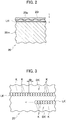
- FIG. 2 is a schematic side cross-sectional view explaining that a peeled substrate is peeled off from a magnesium oxide single crystal substrate in this embodiment.
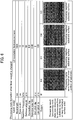
- FIG. 3 is an explanatory view explaining that processing marks are formed in this embodiment.
- a peeled substrate is obtained from a magnesium oxide single crystal substrate (MgO substrate) using a peeled substrate manufacturing apparatus 10 (refer to FIG. 1A ).
- the peeled substrate manufacturing apparatus 10 includes: an XY stage 11; a substrate mounting member 12 (for example, a silicon substrate) held on a stage surface 11f of the XY stage 11; and a laser condensing means 14 (for example, a condenser) for condensing a laser beam B toward a magnesium oxide single crystal substrate 20 mounted on the substrate mounting member 12.
- a laser condensing means 14 for example, a condenser for condensing a laser beam B toward a magnesium oxide single crystal substrate 20 mounted on the substrate mounting member 12.
- the magnesium oxide single crystal substrate 20 is drawn into a rectangular shape when viewed from above; however, may have a wafer shape as a matter of course, and a shape of the magnesium oxide single crystal substrate 20 can be selected freely.
- the XY stage 11 is configured to be capable of adjusting a height position (Z-axis direction position) of the stage surface 11f, in which a distance L between the stage surface 11f and the laser condensing means 14 is made adjustable, that is, a distance between the single crystal substrate on the stage surface 11f and the laser condensing means 14 is made adjustable.
- the XY stage 11 is also configured to be capable of adjusting positions in the XY plane.
- the laser condensing means 14 includes: a correction ring 13; and a condenser lens 15 held in the correction ring 13.
- the laser condensing means 14 has a function to correct an aberration caused by a refractive index of the single crystal substrate 20 made of magnesium oxide, that is, a function as an aberration correction ring.
- the condenser lens 15 when condensing the laser beam B in the air, the condenser lens 15 corrects the laser beam B so that such a laser beam B that has reached an outer peripheral portion E of the condenser lens 15 is condensed closer to the condenser lens 15 than such a laser beam B that has reached a center portion M of the condenser lens 15 is.
- the laser beam B is corrected so that a condensing point EP of the laser beam B that has reached the outer peripheral portion E of the condenser lens 15 is located at a position closer to the condenser lens 15 than a condensing point MP of the laser beam B that has reached the center portion M of the condenser lens 15 is.
- This condenser lens 15 is composed of: a first lens 16 that condenses the laser beam B in the air; and a second lens 18 disposed between this first lens 16 and the single crystal substrate 20.
- each of the first lens 16 and the second lens 18 is defined as a lens capable of condensing the laser beam B in a conical shape.
- a rotational position of the correction ring 13 is adjusted, that is, an interval between the first lens 16 and the second lens 18 is adjusted, whereby it is made possible to adjust an interval between the condensing point EP and the condensing point MP.
- the laser condensing means 14 has a function as a correction ring-attached lens.
- a set lens is usable for the purpose of a variety of aberration corrections and of ensuring a working distance.
- a first step of disposing the laser condensing means 14 in a non-contact manner on an irradiated surface 20r of the magnesium oxide single crystal substrate 20 with less lattice defects (hereinafter, simply referred to as a single crystal substrate 20).
- the laser may be irradiated from the magnesium oxide substrate side.
- a second step is performed.
- the laser beam B is irradiated to the surface of the single crystal substrate 20 and the laser beam B is condensed into an inner portion of the single crystal substrate 20 under designated irradiation conditions using the laser condensing means 14.
- the laser condensing means 14 and the single crystal substrate 20 are two-dimensionally moved relatively to each other.
- processing mark lines LK each of which is composed in such a manner that processing marks K formed by thermal processing are formed in line at an inner portion of a single crystal member, are formed in parallel to one another (for example, refer to FIG. 3 ).
- overlapped line portions DK in which the processing marks K overlap one another are formed in at least a part of the processing mark lines LK, whereby planar peeling is caused from the irradiated surface 20r side.
- the processing marks in this description refer to ranges where the component of the single crystal substrate has scattered from condensed positions by the condensation of the laser beam. On a center portion of each of the ranges (that is, processing marks), a void-shaped air gap like a crater is formed.
- the planar peeling is a concept including a state in which the peeled substrate will be peeled off by receiving slight force even if the peeled substrate is not actually peeled off.
- a relative distance between the laser condensing means 14 and the single crystal substrate 20 is preset so that the laser beam B is focused at a designated height position, that is, so that the laser beam B is focused at a designated depth position from the irradiated surface 20r of the single crystal substrate 20.
- a scanning speed of the laser beam is adjusted so as to overlap the processing marks with one another on at least a part thereof in a scanning direction U of the laser beam B. Furthermore, a scanning direction is set along a crystal orientation of the single crystal substrate.
- the processing marks K are sequentially formed, whereby the planar peeling occurs naturally, and the peeled substrate 20p is formed on the irradiated surface side.
- a mark trace seen as halves of the processing marks K formed by the condensation of the laser beam B is formed on such a laser-condensed side of the peeled substrate.
- This mark trace is such a mark trace looking like a resultant of melting and solidifying a part of the magnesium oxide substrate. This resultant seems to be caused by generation of voids and scattering of the magnesium oxide substrate to peripheries of the voids due to eruption. Moreover, on the other peeled substrate, a mark trace seen as the other halves of the processing marks K is formed. This mark trace is such a mark trace looking like a resultant of melting and solidifying a part of the component of the magnesium oxide single crystal substrate. The following is estimated. That is, by the condensation of the laser beam B, such air gaps are formed between the substrate portions to be peeled off from each other, and these air gaps continue with one another, whereby the planar peeling occurs. Moreover, frequently, the voids are arrayed on one of the peeled surfaces subjected to the planar peeling.
- the designated irradiation conditions of the laser beam B are preset so that the planar peeling occurs naturally as described above.
- the thickness t of the peeled substrate 20p to be formed (refer to FIG. 2 )
- an energy density of the laser beam B at a focal point, and the like set are a variety of values such as a wavelength of the laser beam B to be irradiated, an aberration correction amount (defocus amount) of the condenser lens 15, a laser output, a dot pitch dp of the processing mark K (refer to FIG.
- the obtained peeled substrate 20p is thereafter subjected to post treatment such as polishing of the peeled surface according to needs.
- the thin magnesium oxide single crystal substrate can be obtained easily. Moreover, since the thin magnesium oxide single crystal substrate is obtained by being peeled from the single crystal substrate 20 with less lattice defects, the thin magnesium oxide single crystal substrate thus obtained has less lattice defects.
- the processing marks are overlapped with one another on at least a part thereof in the scanning direction of the laser beam, and accordingly, the processing marks K thus overlapping one another can be formed efficiently.
- FIG. 3 illustrates the example where all of the processing mark lines LK are composed of the overlapped line portions DK
- the planar peeling may be caused from the irradiated surface 20r side by forming the overlapped line portions DK in a part of the processing mark lines LK.
- the time taken to form the processing mark lines LK can be shortened.
- all of the processing mark lines Lk are composed of the overlapped line portions DK, it is easy to cause the planar peeling over the entire surface of the irradiated region.
- the single crystal substrate 20 is used as the single crystal member of the magnesium oxide, and such peeled substrates 20p with the same dimension can be sequentially peeled, thus making it possible to sufficiently increase utilization efficiency of the magnesium oxide single crystal member (that is, to sufficiently suppress an occurrence of chips of the magnesium oxide).
- the scanning direction of the laser beam is set along the crystal orientation of the single crystal substrate 20, it is easy to obtain the laser irradiation that naturally causes the planar peeling.
- the high intensity laser beam is specified by peak power (a value obtained by dividing pulse energy by a pulse width) and a power density (a value per unit area of energy per unit time).
- peak power a value obtained by dividing pulse energy by a pulse width
- power density a value per unit area of energy per unit time.
- a high-output laser can be used in order to increase the power density.
- the high intensity laser beam for use in this embodiment is the laser beam B with a short pulse width and a low laser output, which does not damage the machined substrate.
- a laser beam with a short pulse width (for example, a laser beam with a pulse width of 10 ns or less) is preferable in order to further increase the power density.
- the laser beam with a short pulse width is irradiated as described above, thus making it easy to remarkably increase the power density of the high intensity laser beam.
- the defocus amount can be set by the aberration correction.
- a range of the designated irradiation conditions described above can be greatly widened.
- an abutment member to be brought into surface contact with the peeled substrate 20p may be brought into surface contact with the peeled substrate 20p and may be taken out.
- this abutment member is used as a member to which it is desired that the peeled substrate 20p be pasted, thus making it possible to shorten a pasting step.
- an end edge of the peeled substrate 20p is not completely peeled off from the single crystal substrate 20, then it is also made possible to peel off the peeled substrate 20p from the end edge and take out the peeled substrate 20p while suppressing the peeled substrate 20p from being broken.
- peeling strength at this time is 2 MPa or less, and further, falls down below 1.0 MPa.
- the above embodiment has been described by the example of holding the substrate mounting member 12 on the XY stage 11, mounting the single crystal substrate 20 on the substrate mounting member 12, and irradiating the laser beam B to the single crystal substrate 20.
- this embodiment has been described by the example of obtaining the peeled substrate 20p from the single crystal substrate 20 (magnesium oxide single crystal substrate); however, the material of the peeled substrate 20p is not limited to the single crystal single crystal substrate 20, and the irradiated surface 20r may be subjected to the planar peeling from a single crystal member of magnesium oxide, and the peeled substrate 20p may be obtained.
- the inventors of the present disclosure used the peeled substrate manufacturing apparatus 10 described in the above embodiment, held a silicon wafer as the substrate mounting member 12 on the stage surface 11f of the XY stage 11, and mounted and held a magnesium oxide single crystal substrate 20u (an MgO single crystal substrate; hereinafter, simply referred to as a single crystal substrate 20u occasionally) as the single crystal substrate 20 on this silicon substrate.
- a magnesium oxide single crystal substrate 20u an MgO single crystal substrate; hereinafter, simply referred to as a single crystal substrate 20u occasionally
- a substrate with a crystal orientation of (100) a thickness of 300 ⁇ m and a diameter of 50.8 mm ⁇ was used.
- the laser beam B was irradiated to each irradiation experiment region of the single crystal substrate 20u from the irradiated surface thereof, and at the same time, the laser condensing means 14 and the single crystal substrate 20u were two-dimensionally (in a plane form) moved relatively to each other.
- the laser beam B was irradiated in a line form (linearly), whereby one processing mark line LK (refer to FIG. 3 ) was formed, another processing mark line LK was formed in parallel to this processing mark line LK at a position apart therefrom at a designated amount of offset interval, and still another processing mark line was further formed in a similar way at a position apart therefrom at the designated amount of offset interval.
- irradiation tests of the laser beam were carried out individually for the cases of setting the wavelength of the laser beam B to 1024 nm (laser model M1 (LD-excitation femtosecond laser; pulse width: 10 ps)), 532 nm (laser model M2 (LD-excitation solid-state laser; pulse width: 9 ns)), and 1064 nm (laser model M3 (fiber laser; pulse width: 20 ns, 60 ns). Irradiation conditions and irradiation results are shown in FIG. 4 .
- the power densities in the laser models M2 and M3 when the peak powers thereof are 7.4 kW and 7 kW which are approximate to each other are greatly different from each other. Such a great difference is believed to affect whether it is possible to form the processing marks. That is, factors enabling the formation of the marking marks also include a beam diameter, the pulse width, a repetition frequency, and the like, and among them, the shorter pulse width is effective.
- the laser beam for use in the present disclosure is a high-luminance laser as described above, and preferably, the peak power of the laser beam is 10 kW or more, and the power density obtained from the peak power is 1000 W/cm 2 or more.
- the shorter pulse width is effective in order to increase the power density, and the pulse with is preferably 10 ns or less, more preferably 100 ps or less. The pulse width is still more preferably 15 ps or less.
- the inventors of the present disclosure used the peeled substrate manufacturing apparatus 10 in a similar way to Example 1, set the wavelength of the laser beam B to 1024 nm, that is, used the laser model M1 (LD-excitation femtosecond laser), carried out an irradiation test while individually changing the laser output, the dot pitch dp and the line pitch lp as parameters, and evaluated relationships thereamong. Irradiation conditions and irradiation results are shown in FIG. 5 to FIG. 11 .
- the laser model M1 LD-excitation femtosecond laser
- the output of 0.4 W or less resulted in that the surface of the substrate was not machined.
- the dot pitch of 3.0 ⁇ m or less resulted in that the processing marks were formed in a continuous state.
- the line pitch of 10 ⁇ m or less resulted in that processing lines connected to one another to cause the peeling in the planar direction, that is, the processing marks connected to one another to cause the planar peeling.
- the processing marks formed by thermal processing by the condensation of the laser beam at the inner portion of the single crystal member are formed in a state of being laminated on one another at least partially.
- the processing marks can look like being molten and solidified.
- the magnesium oxide single crystal substrate peeled by the present disclosure can be formed efficiently, and accordingly, the peeled substrate obtained from the magnesium oxide single crystal substrate is useful for a high-temperature superconductive film, a ferroelectric film and the like, and is applicable to the field of semiconductor, the field of display, the field of energy, and the like.
Landscapes
- Engineering & Computer Science (AREA)
- Chemical & Material Sciences (AREA)
- Physics & Mathematics (AREA)
- Optics & Photonics (AREA)
- Plasma & Fusion (AREA)
- Mechanical Engineering (AREA)
- Crystallography & Structural Chemistry (AREA)
- Metallurgy (AREA)
- Materials Engineering (AREA)
- Organic Chemistry (AREA)
- Inorganic Chemistry (AREA)
- Chemical Kinetics & Catalysis (AREA)
- General Chemical & Material Sciences (AREA)
- Oil, Petroleum & Natural Gas (AREA)
- Laser Beam Processing (AREA)
- Crystals, And After-Treatments Of Crystals (AREA)
- Processing Of Stones Or Stones Resemblance Materials (AREA)
- Electromagnetism (AREA)
Abstract
Description
- This application claims priority of Japanese patent application No.
2017-196005 filed October 6, 2017 - The present disclosure relates to a substrate manufacturing method optimum for manufacturing a thin magnesium oxide single crystal substrate.
- A magnesium oxide single crystal substrate is used in the field of semiconductor, the field of display, the field of energy, and the like. In order to manufacture this magnesium oxide single crystal substrate, epitaxially growing this magnesium oxide single crystal substrate into a thin film shape is known as well as crystal-growing the magnesium oxide single crystal substrate into a bulk form and cutting the same into a substrate form (for example, refer to
JP 2001-080996 A - Meanwhile, it is thought that diamond is a semiconductor suitable for a high-frequency/high-output electronic device, and in vapor-phase synthesis as one of synthesis methods thereof, a magnesium oxide substrate or a silicon substrate is used as a base substrate (for example, refer to
JP 2015-59069 A - In recent years, as performance of a semiconductor device has been enhanced, a magnesium oxide single crystal substrate, which is thin and has less lattice defects, has been being required more and more.
- A magnesium oxide substrate (MgO substrate) that is a base substrate in manufacture of the above diamond substrate is expensive, and for example, the magnesium oxide substrate is peeled off and separated while keeping a thickness thereof necessary as a base substrate after subjecting single crystal diamond to gas-phase synthesis, whereby the magnesium oxide substrate becomes reusable as the base substrate. Specifically, for example, if a magnesium oxide substrate with a thickness of 180 µm is obtained and reused from a base substrate of magnesium oxide with a thickness of 200 µm, then it can be expected that significant cost reduction can be achieved in a manufacturing process of the diamond substrate, and that this achievement greatly contributes to cost reduction of the diamond substrate.
- In view of the above problem, it is an object of the present disclosure to provide a substrate manufacturing method capable of easily obtaining the thin magnesium oxide single crystal substrate.
- Incidentally, while a variety of manufacturing methods for obtaining a single crystal silicon substrate have been proposed, the inventors of the present disclosure found a manufacturing method, which is targeted for the magnesium oxide substrate and based on a new processing principle different from that of single crystal silicon, in the present disclosure as a result of earnest study.
- In accordance with an aspect of the present disclosure for solving the above problem, there is provided a substrate manufacturing method including: a first step of disposing a laser condensing means on a surface of a single crystal member of magnesium oxide to be irradiated in a non-contact manner, the laser condensing means being for condensing a laser beam; and a second step of irradiating the laser beam to a surface of the single crystal member and condensing the laser beam into an inner portion of the single crystal member under a designated irradiation condition using the laser condensing means, simultaneously moving the laser condensing means and the single crystal member two-dimensionally (XY plane) relatively to each other, and forming processing mark lines in parallel to one another, each of the processing mark lines being composed by forming processing marks in line at the inner portion of the single crystal member, the processing marks being formed by thermal processing, wherein, in the second step, overlapped line portions in which the processing marks overlap one another are formed in at least a part of the processing mark lines, and planar peeling is caused from the irradiated surface side.
- In accordance with the present disclosure, the substrate manufacturing method capable of easily obtaining the thin magnesium oxide single crystal substrate can be provided.
-
-
FIG. 1A is a schematic perspective view of a peeled substrate manufacturing apparatus for use in an embodiment of the present disclosure, andFIG. 1B is a partially enlarged side view of the peeled substrate manufacturing apparatus for use in the embodiment of the present disclosure. -
FIG. 2 is a schematic side cross-sectional view explaining that a peeled substrate is peeled off from a magnesium oxide single crystal substrate in the embodiment of the present disclosure. -
FIG. 3 is a schematic view explaining that processing marks are being formed in the embodiment of the present disclosure. -
FIG. 4 is an explanatory view showing laser beam irradiation conditions and irradiation results in Example 1. -
FIG. 5 is an explanatory view showing laser beam irradiation conditions and irradiation results in Example 2. -
FIG. 6 is an explanatory view showing laser beam irradiation conditions and irradiation results in Example 2. -
FIG. 7 is an explanatory view showing laser beam irradiation conditions and irradiation results in Example 2. -
FIG. 8 is an explanatory view showing laser beam irradiation conditions and irradiation results in Example 2. -
FIG. 9 is an explanatory view showing laser beam irradiation conditions and irradiation results in Example 2. -
FIG. 10 is an explanatory view showing laser beam irradiation conditions and irradiation results in Example 2. -
FIG. 11 is an explanatory view showing laser beam irradiation conditions and irradiation results in Example 2. - Hereinafter, a description will be given of an embodiment of the present disclosure with reference to the accompanying drawings. In the following description, the same or similar reference numerals are assigned to the same constituents as or similar constituents to those already described, and a detailed description thereof is omitted as appropriate. Moreover, the embodiment shown below is an exemplification for embodying the technical idea of this disclosure, and the embodiment of this disclosure does not specify materials, shapes, structures, dispositions and the like of constituent components to those described below. The embodiment of this disclosure can be implemented while being changed in various ways within the scope without departing from the spirit.
-
FIG. 1A is a schematic perspective view of a peeled substrate manufacturing apparatus for use in an embodiment of the present disclosure (hereinafter, the embodiment will be referred to as "this embodiment"), andFIG. 1B is a partially enlarged side view of the peeled substrate manufacturing apparatus for use in this embodiment.FIG. 2 is a schematic side cross-sectional view explaining that a peeled substrate is peeled off from a magnesium oxide single crystal substrate in this embodiment.FIG. 3 is an explanatory view explaining that processing marks are formed in this embodiment. - In this embodiment, a peeled substrate is obtained from a magnesium oxide single crystal substrate (MgO substrate) using a peeled substrate manufacturing apparatus 10 (refer to
FIG. 1A ). - The peeled
substrate manufacturing apparatus 10 includes: anXY stage 11; a substrate mounting member 12 (for example, a silicon substrate) held on astage surface 11f of theXY stage 11; and a laser condensing means 14 (for example, a condenser) for condensing a laser beam B toward a magnesium oxidesingle crystal substrate 20 mounted on thesubstrate mounting member 12. Note that, inFIG. 1A , the magnesium oxidesingle crystal substrate 20 is drawn into a rectangular shape when viewed from above; however, may have a wafer shape as a matter of course, and a shape of the magnesium oxidesingle crystal substrate 20 can be selected freely. - The
XY stage 11 is configured to be capable of adjusting a height position (Z-axis direction position) of thestage surface 11f, in which a distance L between thestage surface 11f and the laser condensing means 14 is made adjustable, that is, a distance between the single crystal substrate on thestage surface 11f and the laser condensing means 14 is made adjustable. TheXY stage 11 is also configured to be capable of adjusting positions in the XY plane. - In this embodiment, the laser condensing means 14 includes: a
correction ring 13; and acondenser lens 15 held in thecorrection ring 13. The laser condensing means 14 has a function to correct an aberration caused by a refractive index of thesingle crystal substrate 20 made of magnesium oxide, that is, a function as an aberration correction ring. Specifically, as shown inFIG. 1B , when condensing the laser beam B in the air, thecondenser lens 15 corrects the laser beam B so that such a laser beam B that has reached an outer peripheral portion E of thecondenser lens 15 is condensed closer to thecondenser lens 15 than such a laser beam B that has reached a center portion M of thecondenser lens 15 is. That is, in the case of the beam condensation, the laser beam B is corrected so that a condensing point EP of the laser beam B that has reached the outer peripheral portion E of thecondenser lens 15 is located at a position closer to thecondenser lens 15 than a condensing point MP of the laser beam B that has reached the center portion M of thecondenser lens 15 is. - This
condenser lens 15 is composed of: afirst lens 16 that condenses the laser beam B in the air; and asecond lens 18 disposed between thisfirst lens 16 and thesingle crystal substrate 20. In this embodiment, each of thefirst lens 16 and thesecond lens 18 is defined as a lens capable of condensing the laser beam B in a conical shape. Then, a rotational position of thecorrection ring 13 is adjusted, that is, an interval between thefirst lens 16 and thesecond lens 18 is adjusted, whereby it is made possible to adjust an interval between the condensing point EP and the condensing point MP. The laser condensing means 14 has a function as a correction ring-attached lens. - As the
first lens 16, besides a spherical or aspherical single lens, a set lens is usable for the purpose of a variety of aberration corrections and of ensuring a working distance. - Hereinafter, a description will be given of an example of manufacturing the magnesium oxide single crystal substrate that is thin from the magnesium oxide single crystal substrate with reference to the accompanying drawings.
- In this embodiment, performed is a first step of disposing the laser condensing means 14 in a non-contact manner on an
irradiated surface 20r of the magnesium oxidesingle crystal substrate 20 with less lattice defects (hereinafter, simply referred to as a single crystal substrate 20). Note that, though not shown, in the case of peeling off the magnesium oxide substrate while leaving such a thin substrate of the magnesium oxide substrate in the diamond substrate formed using the magnesium oxide substrate as a base substrate, the laser may be irradiated from the magnesium oxide substrate side. - After the first step, a second step is performed. In this second step, the laser beam B is irradiated to the surface of the
single crystal substrate 20 and the laser beam B is condensed into an inner portion of thesingle crystal substrate 20 under designated irradiation conditions using the laser condensing means 14. Simultaneously with the irradiation and the condensation, the laser condensing means 14 and thesingle crystal substrate 20 are two-dimensionally moved relatively to each other. In this way, processing mark lines LK, each of which is composed in such a manner that processing marks K formed by thermal processing are formed in line at an inner portion of a single crystal member, are formed in parallel to one another (for example, refer toFIG. 3 ). At this time, overlapped line portions DK in which the processing marks K overlap one another are formed in at least a part of the processing mark lines LK, whereby planar peeling is caused from theirradiated surface 20r side. - Here, the processing marks in this description refer to ranges where the component of the single crystal substrate has scattered from condensed positions by the condensation of the laser beam. On a center portion of each of the ranges (that is, processing marks), a void-shaped air gap like a crater is formed. Moreover, in this description, the planar peeling is a concept including a state in which the peeled substrate will be peeled off by receiving slight force even if the peeled substrate is not actually peeled off.
- In this second step, in consideration of a thickness of a peeled
substrate 20p (refer toFIG. 2 ) manufactured by the planar peeling described above, a relative distance between the laser condensing means 14 and thesingle crystal substrate 20 is preset so that the laser beam B is focused at a designated height position, that is, so that the laser beam B is focused at a designated depth position from theirradiated surface 20r of thesingle crystal substrate 20. - Moreover, in this embodiment, in the case of overlapping the processing marks with one another, a scanning speed of the laser beam is adjusted so as to overlap the processing marks with one another on at least a part thereof in a scanning direction U of the laser beam B. Furthermore, a scanning direction is set along a crystal orientation of the single crystal substrate.
- The processing marks K are sequentially formed, whereby the planar peeling occurs naturally, and the peeled
substrate 20p is formed on the irradiated surface side. On a laser-condensed side of the peeled substrate, a mark trace seen as halves of the processing marks K formed by the condensation of the laser beam B is formed on such a laser-condensed side of the peeled substrate. - This mark trace is such a mark trace looking like a resultant of melting and solidifying a part of the magnesium oxide substrate. This resultant seems to be caused by generation of voids and scattering of the magnesium oxide substrate to peripheries of the voids due to eruption. Moreover, on the other peeled substrate, a mark trace seen as the other halves of the processing marks K is formed. This mark trace is such a mark trace looking like a resultant of melting and solidifying a part of the component of the magnesium oxide single crystal substrate. The following is estimated. That is, by the condensation of the laser beam B, such air gaps are formed between the substrate portions to be peeled off from each other, and these air gaps continue with one another, whereby the planar peeling occurs. Moreover, frequently, the voids are arrayed on one of the peeled surfaces subjected to the planar peeling.
- The designated irradiation conditions of the laser beam B are preset so that the planar peeling occurs naturally as described above. In this setting of the designated irradiation conditions, in consideration of properties (crystal structure or the like) of the
single crystal substrate 20, the thickness t of the peeledsubstrate 20p to be formed (refer toFIG. 2 ), an energy density of the laser beam B at a focal point, and the like, set are a variety of values such as a wavelength of the laser beam B to be irradiated, an aberration correction amount (defocus amount) of thecondenser lens 15, a laser output, a dot pitch dp of the processing mark K (refer toFIG. 3 ; an interval between adjacent processing marks in the same processing mark line, that is, an interval between a processing mark and a processing mark formed immediately therebefore), and a line pitch lp (refer toFIG. 1A ; an offset pitch: an interval between adjacent processing mark lines). The obtained peeledsubstrate 20p is thereafter subjected to post treatment such as polishing of the peeled surface according to needs. - In accordance with this embodiment, the thin magnesium oxide single crystal substrate can be obtained easily. Moreover, since the thin magnesium oxide single crystal substrate is obtained by being peeled from the
single crystal substrate 20 with less lattice defects, the thin magnesium oxide single crystal substrate thus obtained has less lattice defects. - Moreover, in the case of at least partially overlapping the processing marks with one another, the processing marks are overlapped with one another on at least a part thereof in the scanning direction of the laser beam, and accordingly, the processing marks K thus overlapping one another can be formed efficiently. In addition, it is easy to uniform dimensions of the respective overlapping portions.
- Note that, though
FIG. 3 illustrates the example where all of the processing mark lines LK are composed of the overlapped line portions DK, the planar peeling may be caused from theirradiated surface 20r side by forming the overlapped line portions DK in a part of the processing mark lines LK. In this way, the time taken to form the processing mark lines LK can be shortened. Moreover, when all of the processing mark lines Lk are composed of the overlapped line portions DK, it is easy to cause the planar peeling over the entire surface of the irradiated region. - Moreover, the
single crystal substrate 20 is used as the single crystal member of the magnesium oxide, and such peeledsubstrates 20p with the same dimension can be sequentially peeled, thus making it possible to sufficiently increase utilization efficiency of the magnesium oxide single crystal member (that is, to sufficiently suppress an occurrence of chips of the magnesium oxide). - Further, since the scanning direction of the laser beam is set along the crystal orientation of the
single crystal substrate 20, it is easy to obtain the laser irradiation that naturally causes the planar peeling. - Moreover, in this embodiment, it is desirable to use a high intensity laser beam as the laser beam B. In the present disclosure the high intensity laser beam is specified by peak power (a value obtained by dividing pulse energy by a pulse width) and a power density (a value per unit area of energy per unit time). Generally, a high-output laser can be used in order to increase the power density. Meanwhile, in this embodiment, for example, when the laser beam B is irradiated by such a high output that exceeds 1 kW, such a substrate to be machined is damaged, and the thin processing marks taken as a target cannot be formed. That is, preferably, the high intensity laser beam for use in this embodiment is the laser beam B with a short pulse width and a low laser output, which does not damage the machined substrate.
- A laser beam with a short pulse width (for example, a laser beam with a pulse width of 10 ns or less) is preferable in order to further increase the power density. The laser beam with a short pulse width is irradiated as described above, thus making it easy to remarkably increase the power density of the high intensity laser beam.
- Moreover, in this embodiment, it is possible to implement the aberration correction by the
correction ring 13 and thecondenser lens 15, which are owned by the laser condensing means 14, and in the second step, the defocus amount can be set by the aberration correction. In this way, a range of the designated irradiation conditions described above can be greatly widened. When it is possible to select means for adjusting a depth of forming the processing marks and conditions for thinly forming the processing marks depending on a thickness of the substrate to be machined and a thickness of such a substrate to be peeled off, and the thickness of the magnesium oxide substrate to be machined is 200 to 300 µm, then the above range can be widened effectively by setting the defocus amount to 30 to 120 µm. - Moreover, in the case of taking out the peeled
substrate 20p subjected to the planar peeling from thesingle crystal substrate 20, an abutment member to be brought into surface contact with the peeledsubstrate 20p may be brought into surface contact with the peeledsubstrate 20p and may be taken out. In this way, this abutment member is used as a member to which it is desired that the peeledsubstrate 20p be pasted, thus making it possible to shorten a pasting step. Moreover, when an end edge of the peeledsubstrate 20p is not completely peeled off from thesingle crystal substrate 20, then it is also made possible to peel off the peeledsubstrate 20p from the end edge and take out the peeledsubstrate 20p while suppressing the peeledsubstrate 20p from being broken. Moreover, from a viewpoint of facilitating natural peeling even if nothing is done after the irradiation of the laser beam, it is preferable to establish a state in which peeling strength at this time is 2 MPa or less, and further, falls down below 1.0 MPa. - Moreover, the above embodiment has been described by the example of holding the
substrate mounting member 12 on theXY stage 11, mounting thesingle crystal substrate 20 on thesubstrate mounting member 12, and irradiating the laser beam B to thesingle crystal substrate 20. However, it is also possible to directly mount and hold thesingle crystal substrate 20 on theXY stage 11, and to form the processing marks K by the laser beam B. - Further, this embodiment has been described by the example of obtaining the peeled
substrate 20p from the single crystal substrate 20 (magnesium oxide single crystal substrate); however, the material of the peeledsubstrate 20p is not limited to the single crystalsingle crystal substrate 20, and theirradiated surface 20r may be subjected to the planar peeling from a single crystal member of magnesium oxide, and the peeledsubstrate 20p may be obtained. - The inventors of the present disclosure used the peeled
substrate manufacturing apparatus 10 described in the above embodiment, held a silicon wafer as thesubstrate mounting member 12 on thestage surface 11f of theXY stage 11, and mounted and held a magnesium oxide single crystal substrate 20u (an MgO single crystal substrate; hereinafter, simply referred to as a single crystal substrate 20u occasionally) as thesingle crystal substrate 20 on this silicon substrate. In this example, as the magnesium oxide single crystal substrate 20u to be irradiated with the laser beam, a substrate with a crystal orientation of (100), a thickness of 300 µm and a diameter of 50.8 mmϕ was used. - Then, by the substrate manufacturing method described in the above embodiment, in order to sequentially form the processing marks K at an inner portion of each of irradiation experiment regions of the single crystal substrate 20u, the laser beam B was irradiated to each irradiation experiment region of the single crystal substrate 20u from the irradiated surface thereof, and at the same time, the laser condensing means 14 and the single crystal substrate 20u were two-dimensionally (in a plane form) moved relatively to each other.
- In this example, the laser beam B was irradiated in a line form (linearly), whereby one processing mark line LK (refer to
FIG. 3 ) was formed, another processing mark line LK was formed in parallel to this processing mark line LK at a position apart therefrom at a designated amount of offset interval, and still another processing mark line was further formed in a similar way at a position apart therefrom at the designated amount of offset interval. - Then, in this example, irradiation tests of the laser beam were carried out individually for the cases of setting the wavelength of the laser beam B to 1024 nm (laser model M1 (LD-excitation femtosecond laser; pulse width: 10 ps)), 532 nm (laser model M2 (LD-excitation solid-state laser; pulse width: 9 ns)), and 1064 nm (laser model M3 (fiber laser; pulse width: 20 ns, 60 ns). Irradiation conditions and irradiation results are shown in
FIG. 4 . - In this example, after the laser beam was irradiated, influences from the peak power and power density of the laser beam B in the formation of the processing marks were evaluated.
- In the laser models M1 and M2, conditions enabling the processing marks K to be formed at the inner portion of the single crystal substrate were found; however, in the laser model M3 (fiber laser), the processing marks K were not able to be formed by the irradiation of the laser beam B to the inner portion of the single crystal substrate. The reason for this is believed to be due to lack of the peak power and the power density.
- The power densities in the laser models M2 and M3 when the peak powers thereof are 7.4 kW and 7 kW which are approximate to each other are greatly different from each other. Such a great difference is believed to affect whether it is possible to form the processing marks. That is, factors enabling the formation of the marking marks also include a beam diameter, the pulse width, a repetition frequency, and the like, and among them, the shorter pulse width is effective.
- Preferably, the laser beam for use in the present disclosure is a high-luminance laser as described above, and preferably, the peak power of the laser beam is 10 kW or more, and the power density obtained from the peak power is 1000 W/cm2 or more. Moreover, the shorter pulse width is effective in order to increase the power density, and the pulse with is preferably 10 ns or less, more preferably 100 ps or less. The pulse width is still more preferably 15 ps or less.
- Moreover, the inventors of the present disclosure used the peeled
substrate manufacturing apparatus 10 in a similar way to Example 1, set the wavelength of the laser beam B to 1024 nm, that is, used the laser model M1 (LD-excitation femtosecond laser), carried out an irradiation test while individually changing the laser output, the dot pitch dp and the line pitch lp as parameters, and evaluated relationships thereamong. Irradiation conditions and irradiation results are shown inFIG. 5 to FIG. 11 . - As shown in
FIG. 5 andFIG. 6 , the output of 0.4 W or less resulted in that the surface of the substrate was not machined. Moreover, as shown inFIG. 7 to FIG. 9 , the dot pitch of 3.0 µm or less resulted in that the processing marks were formed in a continuous state. Moreover, as shown inFIG. 10 andFIG. 11 , the line pitch of 10 µm or less resulted in that processing lines connected to one another to cause the peeling in the planar direction, that is, the processing marks connected to one another to cause the planar peeling. - In this example, in order to facilitate the peeling after the irradiation of the laser beam, the processing marks formed by thermal processing by the condensation of the laser beam at the inner portion of the single crystal member are formed in a state of being laminated on one another at least partially. Here, the processing marks can look like being molten and solidified. In this example, it was found that it was possible to evaluate this state by microscopic evaluation from the laser irradiation surface, that is, it was possible to determine that such a state was caused by the continuous formation of the processing marks. Then, this example provided knowledge that it was possible to appropriately select the laser output, the dot pitch dp and the line pitch lp.
- The magnesium oxide single crystal substrate peeled by the present disclosure can be formed efficiently, and accordingly, the peeled substrate obtained from the magnesium oxide single crystal substrate is useful for a high-temperature superconductive film, a ferroelectric film and the like, and is applicable to the field of semiconductor, the field of display, the field of energy, and the like.
-
- 10
- peeled substrate manufacturing apparatus
- 11
- XY stage
- 11f
- stage surface
- 12
- substrate mounting member
- 13
- correction ring
- 14
- laser condensing means
- 15
- condenser lens
- 16
- first lens
- 18
- second lens
- 20
- magnesium oxide single crystal substrate (single crystal member)
- 20p
- peeled substrate
- 20r
- irradiated surface
- 20u
- magnesium oxide single crystal substrate (single crystal member)
- B
- laser beam
- E
- outer peripheral portion
- EP
- condensing point
- K
- processing mark
- LK
- processing mark line
- M
- center portion
- MP
- condensing point
- M1
- laser model
- M2
- laser model
- M3
- laser model
- dp
- dot pitch
- lp
- line pitch
Claims (9)
- A substrate manufacturing method comprising:a first step of disposing a laser condensing means on a surface of a single crystal member of magnesium oxide to be irradiated in a non-contact manner, the laser condensing means being for condensing a laser beam; anda second step of irradiating the laser beam to a surface of the single crystal member and condensing the laser beam into an inner portion of the single crystal member under a designated irradiation condition using the laser condensing means, simultaneously moving the laser condensing means and the single crystal member two-dimensionally relatively to each other, and forming processing mark lines in parallel to one another, each of the processing mark lines being composed by forming processing marks in line at the inner portion of the single crystal member, the processing marks being formed by thermal processing,wherein, in the second step, overlapped line portions in which the processing marks overlap one another are formed in at least a part of the processing mark lines, and planar peeling is caused from the irradiated surface side .
- The substrate manufacturing method according to claim 1, wherein the overlapped line portions are formed over an entirety of the processing mark lines.
- The substrate manufacturing method according to claim 1, wherein a single crystal substrate is used as the single crystal member.
- The substrate manufacturing method according to claim 1, wherein, when being overlapped with one another at least partially, the processing marks are overlapped with one another at least partially in a scanning direction of the laser beam.
- The substrate manufacturing method according to claim 4, wherein the scanning direction is set along a crystal orientation of the single crystal member.
- The substrate manufacturing method according to claim 1, wherein a high intensity laser beam is irradiated as the laser beam.
- The substrate manufacturing method according to claim 6, wherein a laser beam with a pulse width of 10 ns or less is irradiated as the laser beam.
- The substrate manufacturing method according to claim 7, wherein a laser beam with a pulse width of 100 ps or less is irradiated as the laser beam.
- The substrate manufacturing method according to claim 8, wherein a laser beam with a pulse width of 15 ps or less is irradiated as the laser beam.
Applications Claiming Priority (1)
| Application Number | Priority Date | Filing Date | Title |
|---|---|---|---|
| JP2017196005A JP6943388B2 (en) | 2017-10-06 | 2017-10-06 | Substrate manufacturing method |
Publications (2)
| Publication Number | Publication Date |
|---|---|
| EP3467159A1 true EP3467159A1 (en) | 2019-04-10 |
| EP3467159B1 EP3467159B1 (en) | 2023-01-11 |
Family
ID=63685828
Family Applications (1)
| Application Number | Title | Priority Date | Filing Date |
|---|---|---|---|
| EP18197096.3A Active EP3467159B1 (en) | 2017-10-06 | 2018-09-27 | Substrate manufacturing method |
Country Status (6)
| Country | Link |
|---|---|
| US (1) | US20190105739A1 (en) |
| EP (1) | EP3467159B1 (en) |
| JP (1) | JP6943388B2 (en) |
| KR (1) | KR102128501B1 (en) |
| CN (1) | CN109659225B (en) |
| TW (1) | TWI687559B (en) |
Families Citing this family (4)
| Publication number | Priority date | Publication date | Assignee | Title |
|---|---|---|---|---|
| JP6795811B2 (en) * | 2017-02-16 | 2020-12-02 | 国立大学法人埼玉大学 | Peeling substrate manufacturing method |
| JP7121941B2 (en) * | 2018-03-09 | 2022-08-19 | 国立大学法人埼玉大学 | Substrate manufacturing method |
| JP7734363B2 (en) * | 2021-07-02 | 2025-09-05 | 国立大学法人埼玉大学 | Diamond substrate manufacturing method |
| JP2023028581A (en) * | 2021-08-19 | 2023-03-03 | 国立大学法人埼玉大学 | Method for manufacturing magnesium oxide substrate |
Citations (5)
| Publication number | Priority date | Publication date | Assignee | Title |
|---|---|---|---|---|
| JP2001080996A (en) | 1999-09-09 | 2001-03-27 | Fuji Xerox Co Ltd | Thin film structure |
| JP2015059069A (en) | 2013-09-19 | 2015-03-30 | 独立行政法人産業技術総合研究所 | Method for producing single crystal diamond |
| JP2015119076A (en) * | 2013-12-19 | 2015-06-25 | 信越ポリマー株式会社 | Internal processing layer formation single crystal member and manufacturing method therefor |
| WO2016059449A1 (en) * | 2014-10-13 | 2016-04-21 | Evana Technologies, Uab | Method of laser processing for substrate cleaving or dicing through forming "spike-like" shaped damage structures |
| EP3396031A1 (en) * | 2017-04-26 | 2018-10-31 | Shin-Etsu Polymer Co., Ltd. | Substrate manufacturing method |
Family Cites Families (16)
| Publication number | Priority date | Publication date | Assignee | Title |
|---|---|---|---|---|
| JP4659300B2 (en) * | 2000-09-13 | 2011-03-30 | 浜松ホトニクス株式会社 | Laser processing method and semiconductor chip manufacturing method |
| JP4100953B2 (en) * | 2002-04-18 | 2008-06-11 | キヤノン株式会社 | LAMINATE HAVING SINGLE CRYSTAL OXIDE CONDUCTOR ON Si SUBSTRATE, ACTUATOR USING SAME, INKJET HEAD, AND MANUFACTURING METHOD THEREOF |
| KR100616656B1 (en) * | 2005-01-03 | 2006-08-28 | 삼성전기주식회사 | Method and apparatus for manufacturing gallium nitride based single crystal substrate |
| JP5601778B2 (en) * | 2009-02-19 | 2014-10-08 | 信越ポリマー株式会社 | Manufacturing method of semiconductor wafer |
| JP5456382B2 (en) * | 2009-06-17 | 2014-03-26 | 信越ポリマー株式会社 | Method and apparatus for manufacturing semiconductor wafer |
| JP5493107B2 (en) * | 2010-07-09 | 2014-05-14 | 独立行政法人科学技術振興機構 | Method for producing MgO thin film with plane orientation (111) |
| JP5943921B2 (en) * | 2011-08-10 | 2016-07-05 | 日本碍子株式会社 | Stripping method of group 13 element nitride film |
| JP5917862B2 (en) * | 2011-08-30 | 2016-05-18 | 浜松ホトニクス株式会社 | Processing object cutting method |
| JP6044919B2 (en) * | 2012-02-01 | 2016-12-14 | 信越ポリマー株式会社 | Substrate processing method |
| JP2015123466A (en) * | 2013-12-26 | 2015-07-06 | 信越ポリマー株式会社 | Substrate processing device and substrate processing method |
| KR20170028943A (en) * | 2014-07-14 | 2017-03-14 | 코닝 인코포레이티드 | System for and method of processing transparent materials using laser beam focal lines adjustable in length and diameter |
| EP4122633B1 (en) * | 2014-11-27 | 2025-03-19 | Siltectra GmbH | Solid body division by conversion of substances |
| JP6358940B2 (en) * | 2014-12-04 | 2018-07-18 | 株式会社ディスコ | Wafer generation method |
| CN107112205B (en) * | 2015-01-16 | 2020-12-22 | 住友电气工业株式会社 | Semiconductor substrate and manufacturing method thereof, combined semiconductor substrate and manufacturing method thereof |
| JP6452490B2 (en) * | 2015-02-25 | 2019-01-16 | キヤノン株式会社 | Semiconductor chip generation method |
| JP6202695B2 (en) * | 2016-08-30 | 2017-09-27 | 国立大学法人埼玉大学 | Single crystal substrate manufacturing method |
-
2017
- 2017-10-06 JP JP2017196005A patent/JP6943388B2/en active Active
-
2018
- 2018-09-26 CN CN201811126804.0A patent/CN109659225B/en active Active
- 2018-09-27 EP EP18197096.3A patent/EP3467159B1/en active Active
- 2018-09-28 TW TW107134400A patent/TWI687559B/en active
- 2018-10-01 KR KR1020180116849A patent/KR102128501B1/en active Active
- 2018-10-02 US US16/149,631 patent/US20190105739A1/en not_active Abandoned
Patent Citations (5)
| Publication number | Priority date | Publication date | Assignee | Title |
|---|---|---|---|---|
| JP2001080996A (en) | 1999-09-09 | 2001-03-27 | Fuji Xerox Co Ltd | Thin film structure |
| JP2015059069A (en) | 2013-09-19 | 2015-03-30 | 独立行政法人産業技術総合研究所 | Method for producing single crystal diamond |
| JP2015119076A (en) * | 2013-12-19 | 2015-06-25 | 信越ポリマー株式会社 | Internal processing layer formation single crystal member and manufacturing method therefor |
| WO2016059449A1 (en) * | 2014-10-13 | 2016-04-21 | Evana Technologies, Uab | Method of laser processing for substrate cleaving or dicing through forming "spike-like" shaped damage structures |
| EP3396031A1 (en) * | 2017-04-26 | 2018-10-31 | Shin-Etsu Polymer Co., Ltd. | Substrate manufacturing method |
Also Published As
| Publication number | Publication date |
|---|---|
| CN109659225A (en) | 2019-04-19 |
| JP2019069870A (en) | 2019-05-09 |
| TWI687559B (en) | 2020-03-11 |
| US20190105739A1 (en) | 2019-04-11 |
| KR20190039860A (en) | 2019-04-16 |
| CN109659225B (en) | 2023-11-17 |
| KR102128501B1 (en) | 2020-06-30 |
| JP6943388B2 (en) | 2021-09-29 |
| EP3467159B1 (en) | 2023-01-11 |
| TW201915230A (en) | 2019-04-16 |
Similar Documents
| Publication | Publication Date | Title |
|---|---|---|
| JP5875122B2 (en) | Single crystal substrate manufacturing method and internal modified layer forming single crystal member | |
| JP6004338B2 (en) | Single crystal substrate manufacturing method and internal modified layer forming single crystal member | |
| CN108788449B (en) | Substrate manufacturing method | |
| EP3467159B1 (en) | Substrate manufacturing method | |
| US9099546B2 (en) | Workpiece dividing method including two laser beam application steps | |
| CN105364321A (en) | Laser processing method | |
| JP2017071074A (en) | Method for manufacturing internal processed layer forming single crystal substrate, and method for manufacturing single crystal substrate | |
| CN106041329A (en) | Wafer producing method | |
| JP6004339B2 (en) | Internal stress layer forming single crystal member and single crystal substrate manufacturing method | |
| EP3536437B1 (en) | Substrate manufacturing method | |
| WO2013115352A1 (en) | Production method for monocrystalline substrate, monocrystalline substrate, and production method for monocrystalline member having modified layer formed therein | |
| JP6202696B2 (en) | Single crystal substrate manufacturing method | |
| JP6818273B2 (en) | Substrate processing method | |
| JP6202695B2 (en) | Single crystal substrate manufacturing method | |
| JP2015074003A (en) | Internal processing layer-forming single crystal member, and manufacturing method for the same | |
| JP6779486B2 (en) | Substrate processing method and substrate processing equipment | |
| JP2006024782A (en) | Substrate manufacturing method and substrate manufacturing apparatus | |
| JP5143222B2 (en) | Laser processing method | |
| JP2013062526A (en) | Chip manufacturing method | |
| JP5625183B2 (en) | Laser processing equipment | |
| JP6851041B2 (en) | Substrate processing method and substrate processing equipment | |
| JP2020189493A (en) | Method for manufacturing internal processing layer formation single crystal substrate, and method for manufacturing single crystal substrate |
Legal Events
| Date | Code | Title | Description |
|---|---|---|---|
| PUAI | Public reference made under article 153(3) epc to a published international application that has entered the european phase |
Free format text: ORIGINAL CODE: 0009012 |
|
| STAA | Information on the status of an ep patent application or granted ep patent |
Free format text: STATUS: REQUEST FOR EXAMINATION WAS MADE |
|
| 17P | Request for examination filed |
Effective date: 20180927 |
|
| AK | Designated contracting states |
Kind code of ref document: A1 Designated state(s): AL AT BE BG CH CY CZ DE DK EE ES FI FR GB GR HR HU IE IS IT LI LT LU LV MC MK MT NL NO PL PT RO RS SE SI SK SM TR |
|
| AX | Request for extension of the european patent |
Extension state: BA ME |
|
| RBV | Designated contracting states (corrected) |
Designated state(s): AL AT BE BG CH CY CZ DE DK EE ES FI FR GB GR HR HU IE IS IT LI LT LU LV MC MK MT NL NO PL PT RO RS SE SI SK SM TR |
|
| STAA | Information on the status of an ep patent application or granted ep patent |
Free format text: STATUS: EXAMINATION IS IN PROGRESS |
|
| 17Q | First examination report despatched |
Effective date: 20200710 |
|
| GRAP | Despatch of communication of intention to grant a patent |
Free format text: ORIGINAL CODE: EPIDOSNIGR1 |
|
| STAA | Information on the status of an ep patent application or granted ep patent |
Free format text: STATUS: GRANT OF PATENT IS INTENDED |
|
| RIC1 | Information provided on ipc code assigned before grant |
Ipc: C30B 33/06 20060101ALI20220805BHEP Ipc: C30B 29/16 20060101AFI20220805BHEP |
|
| INTG | Intention to grant announced |
Effective date: 20220824 |
|
| GRAS | Grant fee paid |
Free format text: ORIGINAL CODE: EPIDOSNIGR3 |
|
| GRAA | (expected) grant |
Free format text: ORIGINAL CODE: 0009210 |
|
| STAA | Information on the status of an ep patent application or granted ep patent |
Free format text: STATUS: THE PATENT HAS BEEN GRANTED |
|
| AK | Designated contracting states |
Kind code of ref document: B1 Designated state(s): AL AT BE BG CH CY CZ DE DK EE ES FI FR GB GR HR HU IE IS IT LI LT LU LV MC MK MT NL NO PL PT RO RS SE SI SK SM TR |
|
| REG | Reference to a national code |
Ref country code: GB Ref legal event code: FG4D |
|
| REG | Reference to a national code |
Ref country code: CH Ref legal event code: EP |
|
| REG | Reference to a national code |
Ref country code: DE Ref legal event code: R096 Ref document number: 602018045248 Country of ref document: DE |
|
| REG | Reference to a national code |
Ref country code: IE Ref legal event code: FG4D |
|
| REG | Reference to a national code |
Ref country code: AT Ref legal event code: REF Ref document number: 1543465 Country of ref document: AT Kind code of ref document: T Effective date: 20230215 |
|
| REG | Reference to a national code |
Ref country code: LT Ref legal event code: MG9D |
|
| REG | Reference to a national code |
Ref country code: AT Ref legal event code: MK05 Ref document number: 1543465 Country of ref document: AT Kind code of ref document: T Effective date: 20230111 |
|
| PG25 | Lapsed in a contracting state [announced via postgrant information from national office to epo] |
Ref country code: NL Free format text: LAPSE BECAUSE OF FAILURE TO SUBMIT A TRANSLATION OF THE DESCRIPTION OR TO PAY THE FEE WITHIN THE PRESCRIBED TIME-LIMIT Effective date: 20230111 |
|
| PG25 | Lapsed in a contracting state [announced via postgrant information from national office to epo] |
Ref country code: RS Free format text: LAPSE BECAUSE OF FAILURE TO SUBMIT A TRANSLATION OF THE DESCRIPTION OR TO PAY THE FEE WITHIN THE PRESCRIBED TIME-LIMIT Effective date: 20230111 Ref country code: PT Free format text: LAPSE BECAUSE OF FAILURE TO SUBMIT A TRANSLATION OF THE DESCRIPTION OR TO PAY THE FEE WITHIN THE PRESCRIBED TIME-LIMIT Effective date: 20230511 Ref country code: NO Free format text: LAPSE BECAUSE OF FAILURE TO SUBMIT A TRANSLATION OF THE DESCRIPTION OR TO PAY THE FEE WITHIN THE PRESCRIBED TIME-LIMIT Effective date: 20230411 Ref country code: LV Free format text: LAPSE BECAUSE OF FAILURE TO SUBMIT A TRANSLATION OF THE DESCRIPTION OR TO PAY THE FEE WITHIN THE PRESCRIBED TIME-LIMIT Effective date: 20230111 Ref country code: LT Free format text: LAPSE BECAUSE OF FAILURE TO SUBMIT A TRANSLATION OF THE DESCRIPTION OR TO PAY THE FEE WITHIN THE PRESCRIBED TIME-LIMIT Effective date: 20230111 Ref country code: HR Free format text: LAPSE BECAUSE OF FAILURE TO SUBMIT A TRANSLATION OF THE DESCRIPTION OR TO PAY THE FEE WITHIN THE PRESCRIBED TIME-LIMIT Effective date: 20230111 Ref country code: ES Free format text: LAPSE BECAUSE OF FAILURE TO SUBMIT A TRANSLATION OF THE DESCRIPTION OR TO PAY THE FEE WITHIN THE PRESCRIBED TIME-LIMIT Effective date: 20230111 Ref country code: AT Free format text: LAPSE BECAUSE OF FAILURE TO SUBMIT A TRANSLATION OF THE DESCRIPTION OR TO PAY THE FEE WITHIN THE PRESCRIBED TIME-LIMIT Effective date: 20230111 |
|
| PG25 | Lapsed in a contracting state [announced via postgrant information from national office to epo] |
Ref country code: SE Free format text: LAPSE BECAUSE OF FAILURE TO SUBMIT A TRANSLATION OF THE DESCRIPTION OR TO PAY THE FEE WITHIN THE PRESCRIBED TIME-LIMIT Effective date: 20230111 Ref country code: PL Free format text: LAPSE BECAUSE OF FAILURE TO SUBMIT A TRANSLATION OF THE DESCRIPTION OR TO PAY THE FEE WITHIN THE PRESCRIBED TIME-LIMIT Effective date: 20230111 Ref country code: IS Free format text: LAPSE BECAUSE OF FAILURE TO SUBMIT A TRANSLATION OF THE DESCRIPTION OR TO PAY THE FEE WITHIN THE PRESCRIBED TIME-LIMIT Effective date: 20230511 Ref country code: GR Free format text: LAPSE BECAUSE OF FAILURE TO SUBMIT A TRANSLATION OF THE DESCRIPTION OR TO PAY THE FEE WITHIN THE PRESCRIBED TIME-LIMIT Effective date: 20230412 Ref country code: FI Free format text: LAPSE BECAUSE OF FAILURE TO SUBMIT A TRANSLATION OF THE DESCRIPTION OR TO PAY THE FEE WITHIN THE PRESCRIBED TIME-LIMIT Effective date: 20230111 |
|
| REG | Reference to a national code |
Ref country code: DE Ref legal event code: R097 Ref document number: 602018045248 Country of ref document: DE |
|
| PG25 | Lapsed in a contracting state [announced via postgrant information from national office to epo] |
Ref country code: SM Free format text: LAPSE BECAUSE OF FAILURE TO SUBMIT A TRANSLATION OF THE DESCRIPTION OR TO PAY THE FEE WITHIN THE PRESCRIBED TIME-LIMIT Effective date: 20230111 Ref country code: RO Free format text: LAPSE BECAUSE OF FAILURE TO SUBMIT A TRANSLATION OF THE DESCRIPTION OR TO PAY THE FEE WITHIN THE PRESCRIBED TIME-LIMIT Effective date: 20230111 Ref country code: EE Free format text: LAPSE BECAUSE OF FAILURE TO SUBMIT A TRANSLATION OF THE DESCRIPTION OR TO PAY THE FEE WITHIN THE PRESCRIBED TIME-LIMIT Effective date: 20230111 Ref country code: DK Free format text: LAPSE BECAUSE OF FAILURE TO SUBMIT A TRANSLATION OF THE DESCRIPTION OR TO PAY THE FEE WITHIN THE PRESCRIBED TIME-LIMIT Effective date: 20230111 Ref country code: CZ Free format text: LAPSE BECAUSE OF FAILURE TO SUBMIT A TRANSLATION OF THE DESCRIPTION OR TO PAY THE FEE WITHIN THE PRESCRIBED TIME-LIMIT Effective date: 20230111 |
|
| PLBE | No opposition filed within time limit |
Free format text: ORIGINAL CODE: 0009261 |
|
| STAA | Information on the status of an ep patent application or granted ep patent |
Free format text: STATUS: NO OPPOSITION FILED WITHIN TIME LIMIT |
|
| PG25 | Lapsed in a contracting state [announced via postgrant information from national office to epo] |
Ref country code: SK Free format text: LAPSE BECAUSE OF FAILURE TO SUBMIT A TRANSLATION OF THE DESCRIPTION OR TO PAY THE FEE WITHIN THE PRESCRIBED TIME-LIMIT Effective date: 20230111 |
|
| 26N | No opposition filed |
Effective date: 20231012 |
|
| PG25 | Lapsed in a contracting state [announced via postgrant information from national office to epo] |
Ref country code: SI Free format text: LAPSE BECAUSE OF FAILURE TO SUBMIT A TRANSLATION OF THE DESCRIPTION OR TO PAY THE FEE WITHIN THE PRESCRIBED TIME-LIMIT Effective date: 20230111 |
|
| REG | Reference to a national code |
Ref country code: CH Ref legal event code: PL |
|
| PG25 | Lapsed in a contracting state [announced via postgrant information from national office to epo] |
Ref country code: LU Free format text: LAPSE BECAUSE OF NON-PAYMENT OF DUE FEES Effective date: 20230927 |
|
| REG | Reference to a national code |
Ref country code: BE Ref legal event code: MM Effective date: 20230930 |
|
| PG25 | Lapsed in a contracting state [announced via postgrant information from national office to epo] |
Ref country code: LU Free format text: LAPSE BECAUSE OF NON-PAYMENT OF DUE FEES Effective date: 20230927 Ref country code: IT Free format text: LAPSE BECAUSE OF FAILURE TO SUBMIT A TRANSLATION OF THE DESCRIPTION OR TO PAY THE FEE WITHIN THE PRESCRIBED TIME-LIMIT Effective date: 20230111 Ref country code: MC Free format text: LAPSE BECAUSE OF FAILURE TO SUBMIT A TRANSLATION OF THE DESCRIPTION OR TO PAY THE FEE WITHIN THE PRESCRIBED TIME-LIMIT Effective date: 20230111 |
|
| REG | Reference to a national code |
Ref country code: IE Ref legal event code: MM4A |
|
| PG25 | Lapsed in a contracting state [announced via postgrant information from national office to epo] |
Ref country code: IE Free format text: LAPSE BECAUSE OF NON-PAYMENT OF DUE FEES Effective date: 20230927 |
|
| PG25 | Lapsed in a contracting state [announced via postgrant information from national office to epo] |
Ref country code: CH Free format text: LAPSE BECAUSE OF NON-PAYMENT OF DUE FEES Effective date: 20230930 |
|
| PG25 | Lapsed in a contracting state [announced via postgrant information from national office to epo] |
Ref country code: IE Free format text: LAPSE BECAUSE OF NON-PAYMENT OF DUE FEES Effective date: 20230927 Ref country code: CH Free format text: LAPSE BECAUSE OF NON-PAYMENT OF DUE FEES Effective date: 20230930 |
|
| PG25 | Lapsed in a contracting state [announced via postgrant information from national office to epo] |
Ref country code: BE Free format text: LAPSE BECAUSE OF NON-PAYMENT OF DUE FEES Effective date: 20230930 |
|
| PG25 | Lapsed in a contracting state [announced via postgrant information from national office to epo] |
Ref country code: BG Free format text: LAPSE BECAUSE OF FAILURE TO SUBMIT A TRANSLATION OF THE DESCRIPTION OR TO PAY THE FEE WITHIN THE PRESCRIBED TIME-LIMIT Effective date: 20230111 |
|
| PG25 | Lapsed in a contracting state [announced via postgrant information from national office to epo] |
Ref country code: BG Free format text: LAPSE BECAUSE OF FAILURE TO SUBMIT A TRANSLATION OF THE DESCRIPTION OR TO PAY THE FEE WITHIN THE PRESCRIBED TIME-LIMIT Effective date: 20230111 |
|
| PG25 | Lapsed in a contracting state [announced via postgrant information from national office to epo] |
Ref country code: CY Free format text: LAPSE BECAUSE OF FAILURE TO SUBMIT A TRANSLATION OF THE DESCRIPTION OR TO PAY THE FEE WITHIN THE PRESCRIBED TIME-LIMIT; INVALID AB INITIO Effective date: 20180927 |
|
| PG25 | Lapsed in a contracting state [announced via postgrant information from national office to epo] |
Ref country code: HU Free format text: LAPSE BECAUSE OF FAILURE TO SUBMIT A TRANSLATION OF THE DESCRIPTION OR TO PAY THE FEE WITHIN THE PRESCRIBED TIME-LIMIT; INVALID AB INITIO Effective date: 20180927 |
|
| PGFP | Annual fee paid to national office [announced via postgrant information from national office to epo] |
Ref country code: DE Payment date: 20250919 Year of fee payment: 8 |
|
| PGFP | Annual fee paid to national office [announced via postgrant information from national office to epo] |
Ref country code: GB Payment date: 20250919 Year of fee payment: 8 |
|
| PGFP | Annual fee paid to national office [announced via postgrant information from national office to epo] |
Ref country code: FR Payment date: 20250922 Year of fee payment: 8 |
|
| PG25 | Lapsed in a contracting state [announced via postgrant information from national office to epo] |
Ref country code: TR Free format text: LAPSE BECAUSE OF FAILURE TO SUBMIT A TRANSLATION OF THE DESCRIPTION OR TO PAY THE FEE WITHIN THE PRESCRIBED TIME-LIMIT Effective date: 20230111 |