EP3462593A1 - Elektrischer wechselrichter mit niedriger gleichtaktspannung - Google Patents
Elektrischer wechselrichter mit niedriger gleichtaktspannung Download PDFInfo
- Publication number
- EP3462593A1 EP3462593A1 EP17194335.0A EP17194335A EP3462593A1 EP 3462593 A1 EP3462593 A1 EP 3462593A1 EP 17194335 A EP17194335 A EP 17194335A EP 3462593 A1 EP3462593 A1 EP 3462593A1
- Authority
- EP
- European Patent Office
- Prior art keywords
- switch
- bridge
- point
- auxiliary
- phase output
- Prior art date
- Legal status (The legal status is an assumption and is not a legal conclusion. Google has not performed a legal analysis and makes no representation as to the accuracy of the status listed.)
- Withdrawn
Links
Images

Classifications
-
- H—ELECTRICITY
- H02—GENERATION; CONVERSION OR DISTRIBUTION OF ELECTRIC POWER
- H02M—APPARATUS FOR CONVERSION BETWEEN AC AND AC, BETWEEN AC AND DC, OR BETWEEN DC AND DC, AND FOR USE WITH MAINS OR SIMILAR POWER SUPPLY SYSTEMS; CONVERSION OF DC OR AC INPUT POWER INTO SURGE OUTPUT POWER; CONTROL OR REGULATION THEREOF
- H02M7/00—Conversion of ac power input into dc power output; Conversion of dc power input into ac power output
- H02M7/42—Conversion of dc power input into ac power output without possibility of reversal
- H02M7/44—Conversion of dc power input into ac power output without possibility of reversal by static converters
- H02M7/48—Conversion of dc power input into ac power output without possibility of reversal by static converters using discharge tubes with control electrode or semiconductor devices with control electrode
- H02M7/53—Conversion of dc power input into ac power output without possibility of reversal by static converters using discharge tubes with control electrode or semiconductor devices with control electrode using devices of a triode or transistor type requiring continuous application of a control signal
- H02M7/537—Conversion of dc power input into ac power output without possibility of reversal by static converters using discharge tubes with control electrode or semiconductor devices with control electrode using devices of a triode or transistor type requiring continuous application of a control signal using semiconductor devices only, e.g. single switched pulse inverters
- H02M7/5387—Conversion of dc power input into ac power output without possibility of reversal by static converters using discharge tubes with control electrode or semiconductor devices with control electrode using devices of a triode or transistor type requiring continuous application of a control signal using semiconductor devices only, e.g. single switched pulse inverters in a bridge configuration
- H02M7/53871—Conversion of dc power input into ac power output without possibility of reversal by static converters using discharge tubes with control electrode or semiconductor devices with control electrode using devices of a triode or transistor type requiring continuous application of a control signal using semiconductor devices only, e.g. single switched pulse inverters in a bridge configuration with automatic control of output voltage or current
- H02M7/53873—Conversion of dc power input into ac power output without possibility of reversal by static converters using discharge tubes with control electrode or semiconductor devices with control electrode using devices of a triode or transistor type requiring continuous application of a control signal using semiconductor devices only, e.g. single switched pulse inverters in a bridge configuration with automatic control of output voltage or current with digital control
-
- H—ELECTRICITY
- H02—GENERATION; CONVERSION OR DISTRIBUTION OF ELECTRIC POWER
- H02J—CIRCUIT ARRANGEMENTS OR SYSTEMS FOR SUPPLYING OR DISTRIBUTING ELECTRIC POWER; SYSTEMS FOR STORING ELECTRIC ENERGY
- H02J3/00—Circuit arrangements for ac mains or ac distribution networks
- H02J3/38—Arrangements for parallely feeding a single network by two or more generators, converters or transformers
- H02J3/381—Dispersed generators
-
- H—ELECTRICITY
- H02—GENERATION; CONVERSION OR DISTRIBUTION OF ELECTRIC POWER
- H02M—APPARATUS FOR CONVERSION BETWEEN AC AND AC, BETWEEN AC AND DC, OR BETWEEN DC AND DC, AND FOR USE WITH MAINS OR SIMILAR POWER SUPPLY SYSTEMS; CONVERSION OF DC OR AC INPUT POWER INTO SURGE OUTPUT POWER; CONTROL OR REGULATION THEREOF
- H02M7/00—Conversion of ac power input into dc power output; Conversion of dc power input into ac power output
- H02M7/42—Conversion of dc power input into ac power output without possibility of reversal
- H02M7/44—Conversion of dc power input into ac power output without possibility of reversal by static converters
- H02M7/48—Conversion of dc power input into ac power output without possibility of reversal by static converters using discharge tubes with control electrode or semiconductor devices with control electrode
- H02M7/483—Converters with outputs that each can have more than two voltages levels
- H02M7/487—Neutral point clamped inverters
-
- H—ELECTRICITY
- H02—GENERATION; CONVERSION OR DISTRIBUTION OF ELECTRIC POWER
- H02J—CIRCUIT ARRANGEMENTS OR SYSTEMS FOR SUPPLYING OR DISTRIBUTING ELECTRIC POWER; SYSTEMS FOR STORING ELECTRIC ENERGY
- H02J2300/00—Systems for supplying or distributing electric power characterised by decentralized, dispersed, or local generation
- H02J2300/20—The dispersed energy generation being of renewable origin
- H02J2300/22—The renewable source being solar energy
- H02J2300/24—The renewable source being solar energy of photovoltaic origin
-
- H—ELECTRICITY
- H02—GENERATION; CONVERSION OR DISTRIBUTION OF ELECTRIC POWER
- H02M—APPARATUS FOR CONVERSION BETWEEN AC AND AC, BETWEEN AC AND DC, OR BETWEEN DC AND DC, AND FOR USE WITH MAINS OR SIMILAR POWER SUPPLY SYSTEMS; CONVERSION OF DC OR AC INPUT POWER INTO SURGE OUTPUT POWER; CONTROL OR REGULATION THEREOF
- H02M1/00—Details of apparatus for conversion
- H02M1/12—Arrangements for reducing harmonics from ac input or output
- H02M1/123—Suppression of common mode voltage or current
-
- Y—GENERAL TAGGING OF NEW TECHNOLOGICAL DEVELOPMENTS; GENERAL TAGGING OF CROSS-SECTIONAL TECHNOLOGIES SPANNING OVER SEVERAL SECTIONS OF THE IPC; TECHNICAL SUBJECTS COVERED BY FORMER USPC CROSS-REFERENCE ART COLLECTIONS [XRACs] AND DIGESTS
- Y02—TECHNOLOGIES OR APPLICATIONS FOR MITIGATION OR ADAPTATION AGAINST CLIMATE CHANGE
- Y02E—REDUCTION OF GREENHOUSE GAS [GHG] EMISSIONS, RELATED TO ENERGY GENERATION, TRANSMISSION OR DISTRIBUTION
- Y02E10/00—Energy generation through renewable energy sources
- Y02E10/50—Photovoltaic [PV] energy
- Y02E10/56—Power conversion systems, e.g. maximum power point trackers
Definitions
- the invention relates to the field of electrical power conversion.
- the invention relates to an electrical inverter, a method of operating the electrical inverter, a controller for the electrical inverter, a use of the electrical inverter and a photo-voltaic panel arrangement.
- a simple H-bridge inverter For converting the DC voltage from a photo-voltaic panel into an AC voltage, which may be supplied to an electrical grid, a simple H-bridge inverter may be used.
- An H-bridge is composed of two parallel half-bridges, each of which comprises an upper and a lower switch, and may be operated with three voltage levels. Compared to conventional two-level switching, such a three-level operation has a relatively low current ripple.
- inverter types of inverters may be operated with three-level modulation and also may mitigate the high frequency common mode emission in specific operation modes. However, for these inverter types, much more active switches may be needed to achieve a low common mode emission. Examples for such inverter types are T-type inverters and neutral-point-clamped inverters.
- EP 1 369 985 A2 an inverter is proposed, which adds to the conventional H-bridge two active switches and two diodes. This auxiliary circuit is used to separate the DC capacitor terminals from an inductance connected to the output of the inverter during the free-wheeling states of a three-level modulation.
- An aspect of the invention relates to an electrical inverter, which comprises an H-bridge and a further auxiliary circuit for connecting a midpoint or neutral point of a split DC link to phase outputs of the electrical inverter during a free-wheeling state.
- the H-bridge comprises a first half-bridge, which interconnects a positive point and a negative point of the DC link and which provides a first phase output, and a second half-bridge, which interconnects the positive point and the negative point of the DC link and which provides a second phase output.
- the auxiliary circuit comprises a diode bridge, which is interconnected between the first phase output and the second phase output and which has an upper auxiliary point and a lower auxiliary point, an upper auxiliary switch interconnecting the upper auxiliary point with a neutral point of the DC link and a lower auxiliary switch interconnecting the lower auxiliary point with a neutral point of the DC link.
- the diode bridge may be adapted to rectify the two polarities of an output voltage between the phase outputs into a voltage of one polarity provided between the upper and the lower auxiliary point.
- the auxiliary switches may connect the neutral point of the DC link to the upper and lower auxiliary points. In such a way, the phase outputs are connected to the neutral point during free-wheeling.
- the auxiliary circuit may mitigate high-frequency common-mode emissions that would be produced by the H-bridge alone.
- the diode bridge and two auxiliary switches are used to disconnect the positive and negative points of the DC link from the phase outputs.
- the neutral point of the DC link stays connected to the output phases. This may result in a low common mode voltage noise, since during free-wheeling, both voltages of the phase outputs are substantially equal to the neutral point voltage.
- the common mode voltage may be defined as the average of the voltages at the phase outputs relative to the neutral point.
- the differential mode voltage may be the output voltage of the electrical converter, i.e. the difference of the voltages at the phase outputs.
- a switchable conduction direction of the upper auxiliary switch is from the upper auxiliary point to the neutral point.
- the switches as described herein may be switchable by a signal, which controls, whether the switch is conducting or not in at least one direction. In the other direction, the switch may be always conducting.
- a conduction direction may be defined in that the switch has a very low resistance, when a positive voltage is applied to the switch in the direction.
- a switchable conduction direction of the lower auxiliary switch may be from the neutral point to the lower auxiliary point.
- the upper auxiliary switch comprises a semiconductor switch and optionally an antiparallel diode.
- the lower auxiliary switch may comprise a semiconductor switch and optionally an antiparallel diode.
- the auxiliary switches and/or the switches of the H-bridge may comprise transistors or thyristors, such as IGBTs, IGCT, etc., as semiconductor switches.
- the diode bridge may comprise four diodes and/or may be composed solely of diodes.
- the diode bridge may comprise a first upper diode interconnecting the first phase output with the upper auxiliary point in its conducting direction; a second upper diode interconnecting the second phase output with the upper auxiliary point in its conducting direction; a first lower diode interconnecting the lower auxiliary point with the first phase output in its conducting direction; and a second lower diode interconnecting the lower auxiliary point with the second phase output in its conducting direction.
- the first-half-bridge comprises an upper switch and a lower switch, which are series-connected and provide the first phase output between them.
- the second half-bridge may comprise an upper switch and a lower switch, which are series-connected and provide the second phase output between them.
- the auxiliary switches may be series-connected via the neutral point of the DC link.
- the electrical inverter may be composed of three half-bridge modules, each of which comprises two series-connected switches.
- the upper switches and the lower switches have a switchable conduction direction between the positive point and the negative point of the DC link.
- the phase outputs may be connected to the DC link in parallel and antiparallel by accordingly switching the switches.
- each of the upper switches and the lower switches comprises a semiconductor switch and an antiparallel diode.
- the switches of the H-bridge may comprise the same semiconductor switches with the same voltage rating as the auxiliary switches.
- an electrical filter is connected in the first and/or second phase output.
- the electrical filter may be connected between the phase outputs and an electrical grid.
- an inductor may be connected in the first phase output or in the second phase output. It also may be possible that an inductor is connected in both phase outputs.
- the DC link comprises two series-connected capacitors, which provide the neutral point between them.
- the capacitors may have the same voltage rating and/or the same capacity.
- Each of the capacitors may provide half of the DC link voltage.
- the controller may comprise a CPU, which produces switching signals for the switches with a computer program running in the CPU.
- the method is implemented in hardware in the controller.
- the switches of the inverter i.e. the upper switch and the lower switch of the first half-bridge, the upper switch and the lower switch of the second half-bridge, the upper auxiliary switch and the lower auxiliary switch, are switched in such a way, that during free-wheeling, the phase outputs are connected with the auxiliary circuit to the neutral point of the DC link.
- the upper switch of the first half-bridge and the lower switch of the second half-bridge are closed, while the lower switch of the first half-bridge, the upper switch of the second half-bridge, the upper auxiliary switch and the lower auxiliary switch are opened.
- the term "closed” may mean that the corresponding switch is switched into a conducting state in its switchable conduction direction. It may be that also in the opened state, a switch may be conducting in a direction opposite to its conduction direction.
- the lower switch of the first half-bridge and the upper switch of the second half-bridge are closed, while the upper switch of the first half-bridge, the lower switch of the second half-bridge, the upper auxiliary switch and the lower auxiliary switch are opened.
- a free-wheeling switching state in a free-wheeling switching state, at least one of the upper auxiliary switch and the lower auxiliary switch is closed, while the upper switch and the lower switch of the first half-bridge and the upper switch and the lower switch of the second half-bridge are opened.
- the upper switch and the lower switch of the first half-bridge and the upper switch and the lower switch of the second half-bridge are opened.
- the upper auxiliary switch and the lower auxiliary switch are closed. It also may be that both auxiliary switches are closed during free-wheeling. This may result in a rather simple switching scheme.
- the electrical inverter is switched, such that a free-wheeling state is present between two positive and/or negative switching states. It may be that the output current is modulated by switching the output voltage on in short intervals. Between such intervals, the output voltage may be zero and the inverter may be in the free-wheeling switching state.
- the positive switching state, the negative switching state and the free-wheeling switching state are chosen according to pulse width modulation of a sinusoidal reference voltage. This may result in a free-wheeling switching state between two positive and/or negative switching states.
- a further aspect of the invention relates to a photo-voltaic panel arrangement, which comprises an electrical inverter as described in the above and in the following and at least one photo-voltaic panel connected in parallel to the DC link.
- the DC voltage from the at least one photo-voltaic panel may be converted into an AC voltage to be supplied to an electrical grid. Due to the auxiliary circuit, only low common mode noise may be introduced into the electrical grid.
- a further aspect of the invention relates to a use of an electrical inverter as described in the above and in the following for converting a DC voltage from at least one photo-voltaic panel into an AC voltage supplied to an electric grid. Due to its simple design and the simple switching scheme, the electrical converter may be especially suited for a mass market product, such as photo-voltaic energy conversion.
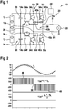
- Fig. 1 shows a photo-voltaic panel arrangement 10 comprising a plurality of series-connected photo-voltaic panels 12, which are connected in parallel to the DC inputs 14a, 14b of an electrical inverter 16.
- the phase outputs 18a, 18b of the electrical inverter are connected via an output filter 20 with an electrical grid 22.
- the output filter 20 may comprise an inductor 21 in one of the phase outputs 18a, 18b and/or an inductor 21 for every phase output 18a, 18b.
- the electrical inverter 16 comprises a DC link 24 with two series-connected DC link capacitors 26, which are connected between a positive point 14a providing an DC input 14a and a negative point 14b providing a further DC output 14b.
- the DC link capacitors 26 provide a neutral point 28 between them.
- the electrical inverter 16 furthermore comprises an H-bridge 30, which is connected between the DC link 24 and the filter 20.
- the H-bridge 30 comprises a first half-bridge 32a, composed of an upper switch 34a and a lower switch 34b, which are series-connected, and a second half-bridge 32b, composed of an upper switch 34c and a lower switch 34d, which are series-connected.
- the half-bridges 32a, 32b are connected in parallel to the DC inputs 14a, 14b of the DC link 24.
- the first half-bridge 32a provides a first phase output 18a between its switches 34a, 34b.
- the second half-bridge 32a provides a second phase output 18b between its switches 34c, 34d.
- the upper switches 34a, 34c and the lower switches 34b, 34d have a switchable conduction direction between the positive point 14a and the negative point 14b of the DC link 24.
- the electrical inverter comprises an auxiliary circuit 36, which comprises a diode bridge 38 and two auxiliary switches 34e, 34f.
- the diode bridge 38 is interconnected between the first phase output 18a and the second phase output 18b and has an upper auxiliary point 40a and a lower auxiliary point 40b.
- the upper auxiliary switch 34e interconnects the upper auxiliary point 40a with the neutral point 28 of the DC link 24 and the lower auxiliary switch 34f interconnects the lower auxiliary point 40b with the neutral point 28 of the DC link 24.
- the diode bridge 38 is adapted for rectifying a voltage of different polarity between the phase outputs 18a, 18b into a voltage of one polarity provided between the auxiliary points 40a, 40b.
- the diode bridge 38 comprises a first upper diode 42a interconnecting the first phase output 18a with the upper auxiliary point 40a in its conducting direction, a second upper diode 42b interconnecting the second phase output 18b with the upper auxiliary point 40a in its conducting direction, a first lower diode 42c interconnecting the lower auxiliary point 40b with the first phase output 18a in its conducting direction, and a second lower diode 42d interconnecting the lower auxiliary point 40b with the second phase output 18b in its conducting direction.
- the upper auxiliary switch 34e and the lower auxiliary switch 34f are series-connected via the neutral point 28.
- the switchable conduction direction of the upper auxiliary switch 34e is from the upper auxiliary point 40a to the neutral point 28 and the switchable conduction direction of the lower auxiliary switch 34f is from the neutral point 28 to the lower auxiliary point 40b.
- the neutral point 28 may be connected with the auxiliary points 40a, 40b, which via the diode bridge 38 provide the rectified phase output voltage.
- the phase outputs 18a, 18b may be set to the same voltage and additionally to the neutral point voltage of the DC link 24.
- Every switch 34a to 34f is composed of a semiconductor switch and an antiparallel diode.
- the diodes of the auxiliary switches 34e, 34f may not be necessary, i.e. each of these switches 34e, 34f may comprise solely a semiconductor switch with one conduction direction.
- the switch 34a to 34f and in particular the semiconductor switches are controlled by a controller 44 of the electrical inverter 16, which may measure currents and/or voltages in the electrical inverter 16 and may switch the switches 34a to 34f as described in the above and the below.
- Fig. 2 shows three diagrams with the output current i L in the phase outputs 18a, 18b, the output or differential mode voltage u DM between the phase outputs 18a, 18b and the common mode voltage u CM of the phase outputs 18a, 18b.
- the differential mode voltage u DM is the difference of the phase output voltage v a of the first phase output 18a (for example relative to the neutral point 28) and the phase output voltage v b of the second phase output 18b (for example relative to the neutral point 28).
- the common mode voltage u CM is the average of the phase output voltage v a of the first phase output 18a and the phase output voltage v b of the second phase output 18b.
- the switches 34a to 34f of the inverter 16 are switched with pulse width modulation to produce a three-level output voltage u DM .
- the upper part of Fig. 2 shows, that this produces a substantially sinusoidal output current i L .
- the output voltage u DM is equal to the DC link voltage.
- the output voltage u DM is equal to the negative of the DC link voltage.
- the output voltage u DM is zero.
- the switches 34e and 34f are switched into a conducting state, the phase outputs 18a, 18b are connected with the neutral point 28 and the common mode output voltage u CM is zero or at least constant, when determined with respect to another potential as the neutral point 28. No common mode noise is produced, which may disturb the electrical grid 22.
- a method for operating the inverter 16, which may be performed by the controller 44, will be described additionally with respect to Fig. 3 and 4 .
- the switches 34a, 34b, 34c and 34d may be switched, that the positive switching state 46, the negative switching state 48 and the free-wheeling switching state 50 are chosen according to pulse width modulation of a sinusoidal reference voltage.
- a free-wheeling switching state 50 is present between two positive and/or negative switching states 46, 48.
- a positive switching state 46 is shown in Fig. 3 , the upper switch 34a of the first half-bridge 32a and the lower switch 34d of the second half-bridge 32b are closed or "on", while the lower switch 34b of the first half-bridge 32a, the upper switch 34c of the second half-bridge 32b, the upper auxiliary switch 34e and the lower auxiliary switch 34f are opened or "off".
- Fig. 3 shows, how the output current i L runs through the inverter 16 during the positive switching state 46.
- Fig. 4 shows a free-wheeling switching state, in which the upper auxiliary switch 34e and the lower auxiliary 34f switch are closed or "on", while the upper switch 34a and the lower switch 34b of the first half-bridge 32a and the upper switch 34c and the lower switch 34d of the second half-bridge 32b are opened or "off".
- Fig. 4 shows, how the output current i L runs through the inverter 16 during the free-wheeling switching state 50.
- the electrical inverter 16 disclosed herein also may be used for rectifying an AC voltage into a DC voltage, which is supplied to a load.
Priority Applications (1)
| Application Number | Priority Date | Filing Date | Title |
|---|---|---|---|
| EP17194335.0A EP3462593A1 (de) | 2017-10-02 | 2017-10-02 | Elektrischer wechselrichter mit niedriger gleichtaktspannung |
Applications Claiming Priority (1)
| Application Number | Priority Date | Filing Date | Title |
|---|---|---|---|
| EP17194335.0A EP3462593A1 (de) | 2017-10-02 | 2017-10-02 | Elektrischer wechselrichter mit niedriger gleichtaktspannung |
Publications (1)
| Publication Number | Publication Date |
|---|---|
| EP3462593A1 true EP3462593A1 (de) | 2019-04-03 |
Family
ID=60001770
Family Applications (1)
| Application Number | Title | Priority Date | Filing Date |
|---|---|---|---|
| EP17194335.0A Withdrawn EP3462593A1 (de) | 2017-10-02 | 2017-10-02 | Elektrischer wechselrichter mit niedriger gleichtaktspannung |
Country Status (1)
| Country | Link |
|---|---|
| EP (1) | EP3462593A1 (de) |
Cited By (1)
| Publication number | Priority date | Publication date | Assignee | Title |
|---|---|---|---|---|
| CN112737070A (zh) * | 2021-01-21 | 2021-04-30 | 华中科技大学 | 基于箝位型三电平变换器的集成驱动充电电路和控制系统 |
Citations (3)
| Publication number | Priority date | Publication date | Assignee | Title |
|---|---|---|---|---|
| EP1369985A2 (de) | 2002-05-15 | 2003-12-10 | Frauenhofer-Gesellschaft zur Förderung der angewandten Forschung e.V. | Wechselrichter zum Umwandeln einer elektrischen Gleichspannung in einen Wechselstrom oder eine Wechselspannung |
| US20050286281A1 (en) | 2004-06-25 | 2005-12-29 | Matthias Victor | Method of converting a direct current voltage from a source of direct current voltage, more specifically from a photovoltaic couse of direct current voltage, into a alternating current voltage |
| CN104300822A (zh) * | 2014-09-26 | 2015-01-21 | 南京邮电大学 | 带续流箝位开关的单相非隔离光伏逆变器的控制方法 |
-
2017
- 2017-10-02 EP EP17194335.0A patent/EP3462593A1/de not_active Withdrawn
Patent Citations (3)
| Publication number | Priority date | Publication date | Assignee | Title |
|---|---|---|---|---|
| EP1369985A2 (de) | 2002-05-15 | 2003-12-10 | Frauenhofer-Gesellschaft zur Förderung der angewandten Forschung e.V. | Wechselrichter zum Umwandeln einer elektrischen Gleichspannung in einen Wechselstrom oder eine Wechselspannung |
| US20050286281A1 (en) | 2004-06-25 | 2005-12-29 | Matthias Victor | Method of converting a direct current voltage from a source of direct current voltage, more specifically from a photovoltaic couse of direct current voltage, into a alternating current voltage |
| CN104300822A (zh) * | 2014-09-26 | 2015-01-21 | 南京邮电大学 | 带续流箝位开关的单相非隔离光伏逆变器的控制方法 |
Cited By (1)
| Publication number | Priority date | Publication date | Assignee | Title |
|---|---|---|---|---|
| CN112737070A (zh) * | 2021-01-21 | 2021-04-30 | 华中科技大学 | 基于箝位型三电平变换器的集成驱动充电电路和控制系统 |
Similar Documents
| Publication | Publication Date | Title |
|---|---|---|
| US9325252B2 (en) | Multilevel converter systems and sinusoidal pulse width modulation methods | |
| US9083230B2 (en) | Multilevel voltage source converters and systems | |
| Yadav et al. | A hybrid 7-level inverter using low-voltage devices and operation with single DC-link | |
| US7310254B2 (en) | AC-to-AC (frequency) converter with three switches per leg | |
| JP5457449B2 (ja) | 電力変換装置 | |
| Stala | A natural DC-link voltage balancing of diode-clamped inverters in parallel systems | |
| JP5977287B2 (ja) | マルチレベルインバータ | |
| US10063162B2 (en) | Multi level inverter | |
| EP2568591A1 (de) | Mehrstufengeklammerte Mehrstufenwandler (MLC2) | |
| WO2013080942A1 (ja) | 電力変換制御装置 | |
| EP3329585B1 (de) | Hybrider modularer mehrstufenumrichter | |
| US11171575B2 (en) | Modular multilevel converter topologies | |
| JP5362657B2 (ja) | 電力変換装置 | |
| WO2013151542A1 (en) | Multilevel converter | |
| Zhang et al. | A novel modulation strategy providing loss balancing and neutral point potential balancing for three-level active neutral-point-clamped converter | |
| EP3462593A1 (de) | Elektrischer wechselrichter mit niedriger gleichtaktspannung | |
| US11601046B2 (en) | Three-phase double t-type four-level rectifier | |
| Farnesi et al. | Soft-switching power converters for efficient grid applications | |
| US20240079967A1 (en) | Quasi multi-level converter | |
| Hasan et al. | Analyses and simulation of three-phase MLI with high value of resolution per switch employing SVM control scheme | |
| US20240079966A1 (en) | Quasi three-level power converter | |
| Gierschner et al. | Five-Level Cascaded Flying-Capacitor Converter | |
| Bharadwaj et al. | Three phase parallel three level inverter fed induction motor using PD modulation scheme | |
| GB2601285A (en) | DC-modulating modular electrical converter system and corresponding method for operation | |
| Rao et al. | An eleven-level inverter system for dual-fed induction motor drive |
Legal Events
| Date | Code | Title | Description |
|---|---|---|---|
| PUAI | Public reference made under article 153(3) epc to a published international application that has entered the european phase |
Free format text: ORIGINAL CODE: 0009012 |
|
| STAA | Information on the status of an ep patent application or granted ep patent |
Free format text: STATUS: THE APPLICATION HAS BEEN PUBLISHED |
|
| AK | Designated contracting states |
Kind code of ref document: A1 Designated state(s): AL AT BE BG CH CY CZ DE DK EE ES FI FR GB GR HR HU IE IS IT LI LT LU LV MC MK MT NL NO PL PT RO RS SE SI SK SM TR |
|
| AX | Request for extension of the european patent |
Extension state: BA ME |
|
| STAA | Information on the status of an ep patent application or granted ep patent |
Free format text: STATUS: THE APPLICATION IS DEEMED TO BE WITHDRAWN |
|
| 18D | Application deemed to be withdrawn |
Effective date: 20191005 |