EP3461069A1 - Procédé d'attribution d'adresses dans un système de bus de données série et n uds de bus pour un tel système de bus de données série - Google Patents
Procédé d'attribution d'adresses dans un système de bus de données série et n uds de bus pour un tel système de bus de données série Download PDFInfo
- Publication number
- EP3461069A1 EP3461069A1 EP18196807.4A EP18196807A EP3461069A1 EP 3461069 A1 EP3461069 A1 EP 3461069A1 EP 18196807 A EP18196807 A EP 18196807A EP 3461069 A1 EP3461069 A1 EP 3461069A1
- Authority
- EP
- European Patent Office
- Prior art keywords
- bus
- addressing
- current
- bus node
- node
- Prior art date
- Legal status (The legal status is an assumption and is not a legal conclusion. Google has not performed a legal analysis and makes no representation as to the accuracy of the status listed.)
- Granted
Links
Images


Classifications
-
- H—ELECTRICITY
- H04—ELECTRIC COMMUNICATION TECHNIQUE
- H04L—TRANSMISSION OF DIGITAL INFORMATION, e.g. TELEGRAPHIC COMMUNICATION
- H04L61/00—Network arrangements, protocols or services for addressing or naming
- H04L61/50—Address allocation
- H04L61/5038—Address allocation for local use, e.g. in LAN or USB networks, or in a controller area network [CAN]
-
- G—PHYSICS
- G06—COMPUTING OR CALCULATING; COUNTING
- G06F—ELECTRIC DIGITAL DATA PROCESSING
- G06F13/00—Interconnection of, or transfer of information or other signals between, memories, input/output devices or central processing units
- G06F13/38—Information transfer, e.g. on bus
- G06F13/42—Bus transfer protocol, e.g. handshake; Synchronisation
- G06F13/4282—Bus transfer protocol, e.g. handshake; Synchronisation on a serial bus, e.g. I2C bus, SPI bus
-
- G—PHYSICS
- G06—COMPUTING OR CALCULATING; COUNTING
- G06F—ELECTRIC DIGITAL DATA PROCESSING
- G06F13/00—Interconnection of, or transfer of information or other signals between, memories, input/output devices or central processing units
- G06F13/38—Information transfer, e.g. on bus
- G06F13/42—Bus transfer protocol, e.g. handshake; Synchronisation
- G06F13/4247—Bus transfer protocol, e.g. handshake; Synchronisation on a daisy chain bus
-
- H—ELECTRICITY
- H04—ELECTRIC COMMUNICATION TECHNIQUE
- H04L—TRANSMISSION OF DIGITAL INFORMATION, e.g. TELEGRAPHIC COMMUNICATION
- H04L12/00—Data switching networks
- H04L12/02—Details
- H04L12/10—Current supply arrangements
-
- H—ELECTRICITY
- H04—ELECTRIC COMMUNICATION TECHNIQUE
- H04L—TRANSMISSION OF DIGITAL INFORMATION, e.g. TELEGRAPHIC COMMUNICATION
- H04L12/00—Data switching networks
- H04L12/28—Data switching networks characterised by path configuration, e.g. LAN [Local Area Networks] or WAN [Wide Area Networks]
- H04L12/40—Bus networks
- H04L12/40006—Architecture of a communication node
- H04L12/40019—Details regarding a bus master
-
- H—ELECTRICITY
- H04—ELECTRIC COMMUNICATION TECHNIQUE
- H04L—TRANSMISSION OF DIGITAL INFORMATION, e.g. TELEGRAPHIC COMMUNICATION
- H04L12/00—Data switching networks
- H04L12/28—Data switching networks characterised by path configuration, e.g. LAN [Local Area Networks] or WAN [Wide Area Networks]
- H04L12/40—Bus networks
- H04L12/40006—Architecture of a communication node
- H04L12/40045—Details regarding the feeding of energy to the node from the bus
-
- H—ELECTRICITY
- H04—ELECTRIC COMMUNICATION TECHNIQUE
- H04L—TRANSMISSION OF DIGITAL INFORMATION, e.g. TELEGRAPHIC COMMUNICATION
- H04L12/00—Data switching networks
- H04L12/28—Data switching networks characterised by path configuration, e.g. LAN [Local Area Networks] or WAN [Wide Area Networks]
- H04L12/40—Bus networks
- H04L12/40052—High-speed IEEE 1394 serial bus
- H04L12/40078—Bus configuration
-
- H—ELECTRICITY
- H04—ELECTRIC COMMUNICATION TECHNIQUE
- H04L—TRANSMISSION OF DIGITAL INFORMATION, e.g. TELEGRAPHIC COMMUNICATION
- H04L12/00—Data switching networks
- H04L12/28—Data switching networks characterised by path configuration, e.g. LAN [Local Area Networks] or WAN [Wide Area Networks]
- H04L12/40—Bus networks
- H04L12/4013—Management of data rate on the bus
-
- H—ELECTRICITY
- H04—ELECTRIC COMMUNICATION TECHNIQUE
- H04L—TRANSMISSION OF DIGITAL INFORMATION, e.g. TELEGRAPHIC COMMUNICATION
- H04L12/00—Data switching networks
- H04L12/28—Data switching networks characterised by path configuration, e.g. LAN [Local Area Networks] or WAN [Wide Area Networks]
- H04L12/40—Bus networks
- H04L12/403—Bus networks with centralised control, e.g. polling
-
- H—ELECTRICITY
- H04—ELECTRIC COMMUNICATION TECHNIQUE
- H04L—TRANSMISSION OF DIGITAL INFORMATION, e.g. TELEGRAPHIC COMMUNICATION
- H04L12/00—Data switching networks
- H04L12/28—Data switching networks characterised by path configuration, e.g. LAN [Local Area Networks] or WAN [Wide Area Networks]
- H04L12/40—Bus networks
- H04L2012/40208—Bus networks characterized by the use of a particular bus standard
- H04L2012/40215—Controller Area Network CAN
-
- H—ELECTRICITY
- H04—ELECTRIC COMMUNICATION TECHNIQUE
- H04L—TRANSMISSION OF DIGITAL INFORMATION, e.g. TELEGRAPHIC COMMUNICATION
- H04L12/00—Data switching networks
- H04L12/28—Data switching networks characterised by path configuration, e.g. LAN [Local Area Networks] or WAN [Wide Area Networks]
- H04L12/40—Bus networks
- H04L2012/40208—Bus networks characterized by the use of a particular bus standard
- H04L2012/40234—Local Interconnect Network LIN
-
- H—ELECTRICITY
- H04—ELECTRIC COMMUNICATION TECHNIQUE
- H04L—TRANSMISSION OF DIGITAL INFORMATION, e.g. TELEGRAPHIC COMMUNICATION
- H04L12/00—Data switching networks
- H04L12/28—Data switching networks characterised by path configuration, e.g. LAN [Local Area Networks] or WAN [Wide Area Networks]
- H04L12/40—Bus networks
- H04L2012/40267—Bus for use in transportation systems
- H04L2012/40273—Bus for use in transportation systems the transportation system being a vehicle
Definitions
- the invention relates to a method for assigning addresses in a serial data bus system and bus node for such a serial data bus system.
- the invention relates generally to self-testable serial data bus systems and methods for assigning bus node addresses within this serial data bus to a chain of bus nodes or to methods and apparatus related to preparing the addressing of the bus nodes.
- bus node addressable by the bus master (hereafter referred to as addressing bus node) is limited, since each bus node initiates a defined current in the bus as part of auto addressing.
- bus shunts one-wire data bus shunt resistors (bus shunts) are inserted in each addressing bus node at which these currents cause a voltage drop on their way to the bus master, in which a current sink is active during the address allocation process.
- the address bus nodes closest to the bus master register a higher voltage drop than the addressing bus node further away from the bus master.
- the voltage across the bus shunt is compared to a threshold.
- the addressing bus node that is the last bus node in the bus node chain from the bus master does not switch its power source off. After a predetermined initialization time, this bus node can assume that it is the last to be addressed addressing bus node in the chain of addressing bus node. It then takes over the bus node address transmitted by the bus master and no longer participates in further initialization runs until the received bus node address is declared invalid by a reset command or another reset condition.
- the electrical resistance of the bus shunt should be as small as possible.
- the addressing system must be able to operate with a negative ground offset.
- the level above the bus shunt must be maximized, requiring the largest possible addressing current.
- the amount of current that must be consumed by the bus master during the address allocation process must not exceed a predetermined value, currently 40mA for LIN buses.
- the DE-B-10 2010 026 431 therefore, does not completely solve the problem of addressing a large number of addressing bus nodes and of sufficiently lowering the resistance of the bus shunt resistor.
- the leads in the DE-B-10 2010 026 431 disclosed technical teaching not to a
- DE-B-10 2010 026 431 Another disadvantage of DE-B-10 2010 026 431 is that for reasons of robustness here too a certain level must be kept free in order to prevent overloading of the master or misaddressing. To minimize the bus shunt resistors and to establish conformity with the LIN bus, it is therefore useful to maximize the DC component in the addressing current. When in the DE-B-10 2010 026 431 however, this value varies by an addressing current level. This unnecessarily reduces the available addressing current level.
- Bus node addressing methods are known which require a bus shunt resistor (R2) within each auto addressing bus node (SL1, SL2, SL3). This resistor has the disadvantage that it degrades the EMC behavior compared to a standard LIN bus node.
- the invention is therefore based on the object to provide a solution which does not have the above disadvantages of the prior art and has further advantages.
- the drive unit may be configured to start adjusting the addressing current from an initial value of substantially zero.
- the current sense circuit may include a resistor between the first connection point and the second connection point, and the output current may be output at the bus line output.
- the drive unit may be further configured to receive the address for bus communication operations after the elapse of the predetermined time after the reception of the start signal.
- the drive unit may obtain the address from a bus master coupled to a downstream end of the bus line.
- adjusting the addressing current may comprise configuring that the addressing current is increased at a first rate and the addressing current is lowered at a second rate, the second rate being higher than the first rate.
- the second rate z. B be at least a factor of ten higher than the first rate.
- the drive unit may be configured to disable the addressing power source after accepting the address, or to receive an instruction indicating termination of an addressing mode and setting the addressing current to a bias current level based on the instruction, or that it contains a control loop with a filter.
- the addressable bus node may be coupled to a bus, wherein the first predetermined value is based in part on a maximum current that a bus master may receive.
- the maximum current that the bus master can receive is equal to a minimum threshold for triggering an error condition
- the first predetermined value may be specified to be a predetermined difference below the maximum current.
- the second predetermined value may be based in part on a number of addressable bus nodes coupled to the bus, or based in part on a number of non-addressable bus nodes coupled to the bus.
- the second predetermined value may be determined as the first predetermined value minus the number of non-addressable bus nodes coupled to the bus multiplied by a specified maximum quiescent current for one of the non-addressable bus nodes.
- assigning an address comprises receiving the address via the bus line on the part of the identified addressable bus node.
- each addressable bus node if it has been provided with an address, deactivates the generation of a respective addressing current assigned to the addressable bus node and its output to the bus line.
- the method steps are repeated without those addressable bus nodes to which an address has already been assigned are repeated.
- the invention further proposes a method for assigning addresses in a serial data bus system, wherein the data bus system has a bus master and bus node and wherein on the one hand the bus master is connected to the bus line and on the other hand, the bus nodes are connected successively to the bus line. At least some of the bus nodes each feed a current flowing to the bus master into the bus line.
- one of the bus nodes is the first bus node connected to the bus line closest to the bus master, while the other bus nodes are connected to the bus line upstream of the first bus node.
- one of the bus nodes is the last bus node furthest from the bus master, while the other bus nodes downstream of this last bus node are connected to the bus line between this bus node and the bus master.
- At least two of the bus nodes are addressing bus nodes to which an address is assigned in each case by the bus master in an addressing phase, while further bus nodes can be standard bus nodes, each with an address already determined before the addressing phase is carried out.
- bus line is understood to mean both a single-wire bus and a two-wire bus, the latter being able to be differentially designed and operated.
- a “bus node” is understood to mean the connection hardware of a bus subscriber via which the bus subscriber is connected to the bus line.
- a bus node thus also includes, for example, a bus transceiver, but above all the normally existing pull-up resistor, which can be regarded as a quiescent current source, and possibly also, for example, the switches (possibly with control) with which a bus user can connect the bus can lay on ground.
- the bus node is not a standard bus node but an addressable addressing bus node, the bus node within the scope of the invention also includes the hardware for feeding in an addressing current with associated current measuring unit and detection, as will be described below ,
- the bus current during the operation of a LIN bus must be below a maximum value. If this value is exceeded, this indicates a short circuit of the bus to ground, which must be detected.
- This basic current is used e.g. the stability of the bus and makes it less sensitive to e.g. electromagnetic interference.
- LIN bus applications have in the past been used to interpose a so-called preselect phase, in which not all bus nodes are addressed, but only one group of bus nodes, the size of the group being selected so that the supply currents are fed all bus nodes of this group the maximum current load of the bus is not exceeded.
- a disadvantage of the LIN application are the shunt resistors in the bus. One strives to choose these resistors as small as possible, for example to minimize losses or to avoid other network problems.
- the addressable subscribers have a bus node with a transceiver, that is, with a hardware connected to the bus line, which additionally are provided with a unit for impressing an addressing current and for measuring addressing currents on the bus line.
- the power supply in the bus line is behind the shunt resistor, which is also on the bus line.
- the bus system has a mix of addressing bus nodes and standard non-addressable bus nodes.
- the standard bus nodes have fixed addresses and do not participate in the auto addressing process. All bus nodes, ie both the standard bus node and the addressing bus node, shape quiescent currents into the bus line when stabilizing the bus line and for uniform bus potential generation over the length of the bus line, or can feed such quiescent currents. Not every standard and / or addressing bus node must forcibly feed this bus current during the auto-addressing phase.
- Each addressing bus node first detects the basic current as the sum of all quiescent currents fed from the standard and addressing bus nodes behind it. The default is a maximum bus current which is somewhat below the current value at which the bus master would detect a fault (eg bus short-circuit) and pull the bus to ground.
- the addressing bus nodes now each feed an addressing current, which is not fed in abruptly.
- the bus node furthest from the bus master measures "its" own addressing current as well as further currents which can be fed in by those bus nodes which are connected farther from the bus master than the considered bus node of the bus line.
- this addressing bus node "knows" that it is now identified. After completing an addressing cycle, it is the only one whose addressing current source supplies an addressing current. If an address were now placed on the bus line, then this addressing bus node would be able to accept the address as its own. Alternatively, an address may have previously been sent from the bus master to all not yet addressed addressing bus nodes, so that now one said addressing bus node accepts this address as its own and the other of the not yet addressed addressing bus nodes discard the bus address.
- the method described above then works particularly advantageously in the case of mixed installation, when the standard bus nodes are located exclusively behind the addressing bus node located furthest away from the bus master. Because then the addressing bus node can detect the sum of the fed from these standard bus node quiescent currents as sum quiescent current. If the standard bus nodes are arranged between the bus master and the first addressing bus node, then this addressing bus node and the further addressing bus nodes located behind it do not know how large the base current composed of the quiescent currents is, since they do not have a quiescent current of the standard Can measure bus node. This could be counteracted by providing each addressing bus node with information about how many standard bus nodes are between the group of addressing bus nodes and the bus master.
- each not yet addressed addressing bus node detects its own fed into the bus addressing current.
- Each addressing bus node knows the maximum allowable maximum addressing current.
- the addressing bus nodes closest to the bus master will detect larger sum currents on the bus line during the addressing phase or during an addressing cycle than those addressing bus nodes which are further connected to the bus line and still addressed further from the bus master. If now all not yet addressed addressing bus node each feed a rising bus current in the bus, so one of the front, i.
- next to the bus master not yet addressed addressing bus node finally drives its addressing current to zero, and this process continues over the next not yet addressed addressing bus node, until finally only one not yet addressed addressing bus node its full addressing current in the Bus line feeds, without that the bus line carries a bus current that is greater than the maximum addressing current.
- This addressing bus node now identified, can now be assigned an address.
- An essential advantage of the method according to the invention is that, at the beginning of an addressing phase, it is clear which addressing current each addressing bus node, which has not yet been addressed, is allowed to feed maximally. This addressing current is the same for all addressing bus nodes. The comparison of the current flowing on the bus line with the maximum addressing current is identical for each addressing bus node, which further simplifies the method according to the invention.
- a special feature can be given if only one of the addressing bus nodes has not yet been addressed. For then either another addressing cycle can be carried out, at the end of which it turns out that exactly this one not yet addressed addressing bus node is identified and can be provided with an address. It is also possible, however, to carry out no further addressing cycle in the case of just one addressing bus node that has not yet been addressed, so that its address not yet addressed by the bus master is assigned to this last not yet addressed addressing bus node Feeds addressing current into the bus line.
- each addressing bus node not yet addressed the enlargement of the addressing current takes place with a certain rate of increase, while the return of the addressing current takes place with a certain reduction rate.
- the reduction rate with which each addressing bus node, which has not yet been addressed, when the maximum bus current or the maximum addressing current is exceeded, reduces its addressing current fed into the bus line is selected to be greater than the slew rate with which each one still non-addressed addressing bus node feeds its addressing current until it is exceeded in the bus line.
- the rise and the decrease rate are expediently defined by a first time constant (for the rise rate) and by a second time constant (for the decrease rate).
- an addressing bus node not yet addressed realizes that it has to reduce its addressing current in order to comply with the maximum addressing current on the bus line, this should be done much faster than the further increase of the addressing currents coming from the other addresses not yet addressed Bus node fed into the bus line become.
- the other not yet addressed addressing bus nodes may not notice it because they detect a bus current due to the fact that they measure other sum currents on the bus line more or less significantly less than the maximum addressing current.
- these not yet addressed addressing bus node continue to feed their addressing current until the first of these other not yet addressed addressing bus node notes that the maximum addressing current load is reached, then as a result also to reduce its addressing current.
- This whole process makes it convenient to perform the return of an addressing current at a significantly greater rate of reduction than the rise of the addressing currents.
- the second time constant, ie the reduction rate should expediently be smaller by at least the factor 2 or 5 or 10 or 20 or 50 or 100 or 200 or 500 or 1000 than the first time constant, ie the rate of increase.
- the first and / or the second time constant can each depend on the size of the bus current determined by a not yet addressed addressing bus node or on the size of the address bus node which has not yet been addressed depend on the supplied addressing current or be selected depending.
- the first time constant is greater than or above the threshold value, or smaller than or below the threshold value and / or the second time constant starting at or below the threshold value is or is at or above the threshold .
- each addressing bus node not yet addressed receives a corresponding message sends over the not yet done address assignment to the bus master.
- so many addressing cycles can be carried out in the addressing phase until it is ascertained in one addressing cycle, in particular by the bus master, that none of the addressing bus nodes feeds the maximum addressing current into the bus line.
- the number of bus nodes to be addressed before the beginning of the addressing phase and thus the number of addressing cycles to be performed is known, it can be checked after completion of the addressing phase whether an addressing has been assigned to each addressing bus node.
- the identification of the respective not yet addressed addressing bus node takes place, as soon as it is determined within the addressing cycle, and thus potentially before the end of the predetermined period of the addressing cycle, that one of the not yet addressed addressing bus nodes feeds the maximum addressing current into the bus line.
- At least one standard bus node is connected to the bus line downstream of an addressing bus node with an address already determined before the addressing phase, and for this addressing bus node to provide information about the number of standard addresses located downstream of this addressing bus node.
- Bus node receives and thus knows a possible maximum of the sum of the fed from these standard bus node in the bus line quiescent currents.
- the current measuring means detects the addressing current of the addressing current source to be fed into the bus line and the drive unit compares the addressing current with a predefinable maximum addressing current.
- the current measuring means can be integrated into the bus line and detects the bus current and that the drive unit compares the bus current with a predetermined maximum bus current.
- the rate of increase is defined by a first time constant and the rate of reduction by a second time constant and that the second time constant is smaller by at least a factor of 2 or 5 or 10 or 20 or 50 or 100 or 200 or 500 or 1000 the first time constant.
- the first and / or the second time constant in each case depending on the size of the bus current determined by a not yet addressed addressing bus node or in dependence on the size of the not yet addressed addressing bus node is selected in the addressing bus node input addressing current.
- the first and / or the second time constant in each case is different depending on whether the determined by a not yet addressed addressing bus node bus or that of a not yet addressed addressing bus node in the Bus line fed addressing current is greater than or equal to a threshold value or less than the threshold value or alternatively greater than a threshold value or less than or equal to the threshold value.
- another aspect of the invention is concerned with a method of injecting addressing currents into the bus of a serial data bus system via addressing bus nodes, the data bus system having a bus line in addition to a bus master and the addressing bus node and optionally standard bus nodes on the one hand, the bus master is connected and to the other hand, the bus nodes are connected sequentially.
- the bus line can have a single-wire bus or a two-wire bus, which may be differentially, i. operated with differential signals.
- the method according to the invention ensures that, irrespective of swapping the inputs and outputs of an addressing bus node, via which the bus node is integrated into the serial data bus, the feed of the addressing current always takes place in such a way that it is fed in Addressing current that flows in the direction of bus master, in any case by the current measuring means, which is connected in the bus line flows or is detected by the current measuring means.
- each addressing bus node or at least some of the addressing bus nodes have two addressing power sources which are operatively connected to the bus line via a respective node.
- the current measuring means or the current measuring means itself is in operative connection with the bus line, namely with that portion of the bus line which lies between the two said nodes.
- the latter has a switching unit with an operative connection to the addressing current source standing input and two outputs, one of which is connected to the one node and the other to the other node, wherein the input of the switching unit is selectively engageable with the one output or with the other output in operative connection and wherein the switching unit Mandatory of the drive unit in that switching position can be transferred, in which the current measuring means detects a current flowing through the switching unit addressing current or test current.
- the latter has a first and a second addressing current source, one of which is connected to one node and the other to the other node, and a monitoring unit for determining in which of the two nodes in the case of infeed an addressing current or a test current, the current measuring means detects this current, wherein the addressing current is to be fed from the addressing current source into the bus line which is connected to the node at which the current measuring means has previously detected the current when the addressing current or alternatively the test current is supplied.
- a bridging switch is thus provided per current measuring means which, like the current measuring means, advantageously belongs to the addressing bus node and is driven by the latter depending on whether or not the relevant addressing bus node is already provided with an address.
- the bypass switch is open. Addressing bus nodes already addressed control the bypass switch in such a way that it is now closed and thus the current measuring means is bypassed.
- the addressing phase has a plurality of addressing cycles, wherein one address is assigned to each of the addressing bus not addressed or not yet addressed, and that an addressing bus node addressed in an addressing cycle starts from there no longer participates in the further addressing for other not yet addressed addressing bus subscribers, wherein in the addressing phase an already addressed Adressier bus node associated current measuring means is bridged by closing the parallel to the current measuring means bridging switch.
- bypass switch it is possible to close the bypass switch as soon as an addressing bus node has received its address.
- several addressing bus nodes to be addressed are to be provided with addresses in an addressing phase and thus several addressing cycles have to be run through in the addressing phase, one of the still open bypass switches can be closed after each addressing cycle.
- all current measuring means are "active", which is advantageous insofar as the same "ratios" always exist on the bus line during the addressing phase, namely that all current measuring means are always connected in the bus line.
- each addressing bus node which is not addressed or not yet addressed feeds into the bus line an addressing current flowing to the bus master which flows through the current measuring means of the relevant address bus node which has not yet been addressed.
- the current measuring means detects inter alia the addressing current fed into the bus line by the addressing current source.
- Such an addressing bus node is thus suitable, for example, for an addressing method in which the addressing current, which each addressing bus node, which has not yet been addressed, feeds into the bus line is immediately detected.
- the current flowing in the amount of the addressing bus node on the bus line thus also contains, as a proportion, the addressing current fed by the relevant addressing bus node.
- Such an addressing method will be discussed in more detail below.
- the viewing direction from a bus node is such that everything in the data bus between the bus node and bus master is BEFORE the bus node under consideration and thus the direction of the current flowing to the bus master located downstream of the considered bus node, and everything that is located between the considered bus node and the end of the data bus, located AFTER the bus node and thus with respect to the current direction upstream of the considered bus node.
- the Local Interconnect Network also called LIN bus, is a serial communication system for the networking of sensors and actuators, ie a fieldbus. LIN is used where the bandwidth and versatility of CAN are not needed. Typical application examples are the networking within the door or the seat of a motor vehicle.
- the relevant standard is ISO standard 17987-1, "Road vehicles - Local interconnect network (LIN) - Part 1-7".
- bus shunt resistor (R2) of the respective bus node (SL1, SL2, SL3) is in each case arranged in front of the respective auto-addressing current source (Iq1, Iq2, Iq3), so that the own addressing current of the respective bus node supports this bus node.
- Shunt resistor (R2) must flow through to get to the bus master (ECU) where it is dissipated to ground.
- a further aspect of the invention presented here is, moreover, that from the output of each addressing bus node during the address allocation process, in contrast to all the above-mentioned documents, a substantially constant output current (i j ) of the relevant bus node (SL j ) into the preceding data bus in Direction bus master (ECU) is fed.
- a problem may be present standard bus nodes (CS1, CS2), which have no ability to Autoadress réelle in the context of the invention, that is, have predetermined addresses.
- the standard bus node (CS1, CS2) without auto-addressing capability feed their bus power source (S1, R3, d1) respectively a bus current, the bus node ground current, into the data bus in the direction of the bus master (ECU).
- these are bus nodes (CS1, CS2) which are present only once in the data bus and are therefore easily visually distinguishable from one another by the fitters because of their appearance, for example during assembly of a motor vehicle.
- Each of these standard bus nodes feeds a fundamental (quiescent) current component into the data bus by means of a pull-up current source (S1, R3, d1) according to the LIN standard.
- These standard bus nodes thus together cause a maximum background current.
- This basic current can be estimated by the address addressing bus nodes with auto addressing capability, hereinafter referred to as auto addressing bus node, based on the delivery of the number of standard bus nodes without auto addressing capability.
- n standard bus nodes that have no ability to auto-address, seen from the bus master (ECU) behind z.
- the maximum number n of standard bus nodes behind the two auto addressing bus nodes with auto address capability is then (n + 2) ⁇ I max / I k .
- I max is the maximum current value that the bus master (ECU) can record in the auto-addressing phase according to the ISO standard.
- the maximum current value I max is selected a little less than the true maximum current value of the bus master (ECU) to intercept manufacturing variations and operating parameter variations.
- I k is the upper limit value for the value of the bus node ground current which the entirety of all standard bus nodes without auto-addressing capability feeds into the data bus.
- each of the standard bus nodes without auto-addressing will feed approximately the same bus node ground (idle) stream into the data bus.
- the auto address bus nodes in an upstream phase A can measure this base current through their respective bus shunt resistor (R2) and then determine the current range for the maximum addressing current of each auto address bus node and then use it for auto addressing.
- the voltage drop across the bus shunt resistors (R2) is maximum.
- configuration B all n standard bus nodes that have no ability to autoaddress, as seen from the bus master (ECU) before the z.
- the auto address bus nodes can now receive no information about the number of standard bus nodes in the direction of the bus master (ECU) before them, ie, downstream of them.
- ECU bus master
- the maximum addressing current used by the auto-addressing bus nodes in combination with the base-master current arriving at the bus master of all preceding bus nodes in the data bus is too great, which would result in an error message.
- the maximum number n of standard bus nodes behind the two Autoaddressing bus nodes with auto-addressing capability is again (n + 2) ⁇ I max / I k .
- I max is again the maximum current value which the bus master (ECU) can record in the auto-addressing phase.
- the maximum current value I max is also chosen to be slightly smaller than the true maximum current value of the bus master (ECU) in order to intercept manufacturing fluctuations and operating parameter fluctuations.
- I k is the upper limit of the value of the bus node ground current which the entirety of all standard bus nodes feed into the data bus.
- each of the standard bus nodes feeds in about the same bus node ground current in the data bus.
- I G n * I k at the input of the bus master (ECU).
- I a addressing current
- This area of power can be used by the following auto-address bus nodes with auto addressability, however, received no information.
- this stream area can be used for auto-addressing, the auto-addressing bus node with auto addressing capability must now be notified by the bus master (ECU).
- Configuration C is a mixture of Configuration A and Configuration B.
- the bus master ECU
- the auto addressing bus nodes can determine the total background current by summing this base current with n times the bus node base current I k by measuring the base current through its bus shunt resistor with respect to the subsequent bus nodes.
- the bus master ECU
- each auto address bus node can then recalculate and maximize the maximum addressing current I amax .
- the bus master (ECU) preferably signals to all bus nodes which configuration of the above configurations exists and how many standard bus nodes are present in the system which have no auto-addressing capability and / or how large the expected base bus current is.
- the bus master ECU pulls the data line to ground by means of a switch (SB) or the like.
- the current sink used for this purpose can absorb the maximum current value I max . If this value is exceeded by the amount of bus current in the bus master (ECU), the bus master (ECU) can assume a short circuit and corresponding signaling and error messages produce. Therefore, this maximum current value I max must not be exceeded in normal operation in terms of amount.
- each bus node can then calculate the maximum addressing current I amax of its respective addressing current source (Iql, Iq2, Iq3), which is still permissible without the maximum permissible addressing current (I max ).
- this value is given by the received number n of the standard bus nodes without Autoaddress réellesrote in each Autoadressier bus node with Autoadress réellesttle.
- a safety margin is preferably taken into account, so that the actually set auto-addressing current I amax of the auto-addressing current sources of the auto-addressing bus nodes (SL1, SL2, SL3) is lower than the actual maximum permissible auto-addressing current.
- the total current (i1, i2, i3) is detected, which leaves the respective Autoadressier bus node via the data bus in the direction of the bus master (ECU).
- This is made up of the bus current fed in by the following auto-addressing bus nodes and possibly standard bus nodes, plus the self-supplied addressing current.
- the respective Autoadressier bus node (SI1, SL2, SL3) measures the outgoing bus current (i1, i2, i3) coming from the subsequent Autoadressier bus node (SI2, SI3) the bus shunt (R2) of the respective Autoadressier bus node (SI1, SL2, SL3) flows through and at the output of the respective bus node this leaves again in the direction of the bus master (ECU).
- the respective auto-addressing bus node (SL1, SL2, SL3) now controls its own addressing current source (Iq1, Iq2, Iq3) such that the sum of incoming bus current of the subsequent bus nodes (SI2, SI3) and addressing current of the own addressing current source (Iql, Iq2, Iq3) corresponds to a predetermined total current (I s ).
- the amplitude of the addressing current (I a ) is adjusted so that the maximum bus current I max by the amount of the outgoing bus current (i1, i2, i3) can not be exceeded.
- bus current (1, i2, i3) leaving the respective bus node (SL1, SL2, SI3) remains constant and is not increased by the respective bus node (SL1, SL2, SI3) above a maximum value. An overload of the bus master current sink during the address allocation process is thus excluded.
- each of the auto-addressing bus nodes participating in the address allocation method therefore detects an additional current deviating from the base current.
- This additional power is composed of the own addressing current of the respective bus node and the addressing current of the bus node (addressing bus node and optionally standard bus node) following the respective auto-addressing bus node (SL1, SL2, SL3).
- the respective bus node regulates its output current (i1, i2, i3) in the direction of the bus master (ECU) in such a way that it always corresponds to the intended maximum value of Addressing current I amax plus corresponds to the base current .
- the addressing current source Iq1, Iq2, Iq3 is designed to be controllable within each auto-addressing bus node (SL1, SI2, SI3) with auto addressing capability.
- the addressing current of the respective addressing current source (Iq1, Iq2, Iq3) depends then on the one hand on the previously determined maximum value (I amax ) and on the other hand on a control signal by means of a controlled system (F) and a measuring device (R2, D1) from the Output current (i1, i2, i3) of the respective bus node (SL2) in the direction of bus master (ECU) is determined.
- the controlled system thus begins with a measuring device, preferably a bus shunt resistor (R2), which upstream of that bus node, as seen from the bus master (ECU) between the respective bus node (SL1, SL2, SL3) is preceded in the data bus is.
- a measuring device eg an operational amplifier (D1) and if necessary after filtering (F) converted to a control value, with which the respective Autoadress istsstrom provoke (Iq1, Iq2, Iq3) can then be controlled so that the bus current (i1, i2, i3) is kept constant in the direction of the bus master (ECU) in this address allocation phase.
- this control variable is directly proportional to the respective output current (i1, i2, i3) of the respective auto-addressing bus node (SI1, SI2, SI3) in the direction of the bus master (ECU).
- this control value still exceeds a predefined threshold value (SW) after expiry of the said predetermined initialization time, ie if the individual addressing current source (Iq1, Iq2, Iq3) supplies the predetermined output current in the direction of the bus master (ECU), then the respective auto-addressing bus node is disconnected from the bus master (FIG. ECU) as the last in the chain of auto address bus nodes.
- the relevant auto-addressing bus node then takes over the bus node address to be assigned by the bus master (ECU) previously or subsequently to all auto-addressing bus nodes (SL1, SL2, SI3) as its now valid bus node address and does not participate in further initialization runs, unless that the received bus node address is invalidated by a reset command or any other reset condition.
- the other auto addressing bus nodes that do not yet have a valid bus node address participate in subsequent initialization passes.
- the regulation of the output current value of the auto addressing current sources (Iq1, Iq2, Iq3) within the auto address bus nodes (SL1, SL2, SL3) is filtered by means of a filter (F).
- the control loop forms a PI controller. This filtering is necessary in order to avoid overshoots in the generation of the addressing current by the entirety of the auto-addressing bus nodes (SL1, SI2, SI3) at the bus master (ECU). If this were to happen, then the maximum permissible bus current I max can be exceeded and the bus master (ECU) can detect a short circuit, which should be avoided.
- each auto-addressing bus node SL1, SL2, SI3
- the filter (F) is designed to be non-linear.
- a first control time constant ( ⁇ 1 ) of the non-linear filter (F) for increasing the addressing current of the respective addressing current source (Iq1, Iq2, Iq3) of the respective bus node (SL1, SI2, SI3) should be greater than a second control time constant ( ⁇ 2 ) of the non-linear filter (F) for lowering the addressing current of the respective addressing current source (Iq1, Iq2, Iq3) of the respective bus node (SL1, SL2, SL3).
- the second time constant ( ⁇ 2 ) defining the reduction of the addressing current of the respective addressing current source (Iq1, Iq2, Iq3) should be shorter than the first time constant ( ⁇ 1 ) by a factor m, which defines the increase of the addressing current of the respective addressing current source (Iq1, Iq2, Iq3).
- the addressing current of the respective addressing current source (Iq1, Iq2, Iq3) of the respective bus node (SL1, SL2, SI3) is reduced faster than it is increased.
- subsequent auto-address bus nodes lower their addressing current faster than it is up-regulated by other auto-addressing bus nodes.
- a car addressing bus node having auto-addressing capability After having received a valid bus node address in this manner, a car addressing bus node having auto-addressing capability preferably uses its addressing power source as a bus node ground power source and then behaves like a bus node without auto-addressing capability.
- bus node ground power sources S1, R3, d1 in the Autoadressier bus node (SL1, SL2, SL3) are located. These would then be eliminated.
- This state of a car addressing bus node after the successful assignment of a valid bus node address is preferably changed only by resetting the auto addressing bus node or deleting the validity of the bus node address.
- the bus receives the information from the bus master (ECU) last Autoadressier bus node is a valid Busknotendresse and behaves from there like a standard bus node, so does not participate in the further Autoadress réellesvon.
- the auto addressing bus nodes that have not yet received a valid bus node address continue to behave like auto addressing bus nodes.
- the bus master then triggers another initialization pass in which the penultimate auto-addressing bus node seen by the bus master (ECU), which is now the last auto-addressing bus node seen by the bus master acting as such, receives a valid bus node address. and so on.
- This repetitive triggering of the initialization passes by the bus master (ECU) and the assignment of a valid bus node address in such an initialization pass to the last known from the bus master Autoaddressier bus node behaving as such, is performed until all Autoadressier bus node is a valid Bus node address received from the bus master (ECU).
- the bus master (ECU) preferably checks, after each initialization run, whether the addressed auto-address bus node, which should have just received a valid bus node address, responds.
- the addressed auto-addressing bus node then sends a random number to the bus master (ECU) at the behest of the bus master (ECU).
- bus collisions occur. These can be detected by the bus nodes and signaled to the bus master (ECU). In certain cases, when the answer is predeterminable, the bus master (ECU) can also detect a bus collision directly. As a result, the bus master (ECU) can either directly or indirectly detect a bus collision and possibly repeat the initialization of the relevant bus node address. For this it makes sense if the bus master (ECU) can issue an erase command for the last assigned bus node address to all bus nodes.
- the second time constant ( ⁇ 2 ) is smaller than the first time constant ( ⁇ 1 ) by a factor greater than 10, preferably greater than 100.
- the first time constant ( ⁇ 1 ) within the respective auto-addressing bus node (SLj) depends on the value of the bus node output current (i j ) of the relevant auto-addressing bus node (SL j ) detected by means of measuring means (R2, D1, D3) ).
- the first time constant ( ⁇ 1 ) is very short at the beginning, when the total current through the bus shunt resistor is still small and thus the addressing current source of the respective auto-addressing bus node very quickly increases the current, while later Addressing current of the auto-addressing power source is slowly increased. It is thus conceivable for the first time constant ( ⁇ 1 ) within the relevant auto-addressing bus node (SLj) to be from the value of the bus node output current (i j ) of the relevant auto-addressing bus node (SL j ) detected by means of measuring means (R 2, D 1, D 3). depends in the way that the value of the first time constant ( ⁇ 1 ) has a first value below a threshold value and a second value above the threshold value.
- a variant of the method preferably includes checking the detected value of the bus node output current (i j ) of the relevant auto addressing bus node (SL j ) for plausibility and initiation of measures if the detected value of the bus node output current (i j ) of the respective auto-addressing bus node (SL j ) is not plausible.
- a signaling of a fault via the data bus can be made as requested by a bus master (ECU) if the detected value of the bus node output current (i j ) of the relevant auto-addressing bus node (SL j ) is not plausible.
- a further measure which is necessary to the stability of the control loop, in a refinement of the execution of the step of detecting the value of the Busknotenausgangsstroms (i j) of the relevant Autoadressier bus node (SL j) by means of measuring means (R2, D1, D3) to be.
- the value of the bus node output current (i j ) of the relevant auto-addressing bus node (SL j ) is detected by means of measuring means (R2, D1, D3) with a first sign, if the detected value of the bus node output current (i j ) of the relevant auto-addressing bus node (SL j ) is plausible, and detecting the value of the bus node output current (i j ) of the respective Autoaddressier bus node (SL j ) by means of measuring means (R2, D1, D3) with a second sign, which is inverted to the first sign, if detected value of the bus node output current (i j ) of the relevant Autoaddressing bus node (SL j ) is not plausible.
- Another procedural measure may be the use of a predetermined error address as a valid bus node address of the respective Autoaddressier bus node (SLj), if the detected value of the bus node output current (i j ) of the respective Autoaddressier bus node (SL j ) is not plausible.
- This can be structurally predetermined or specified for example by broadcast message by the bus master (ECU).
- a data bus system with bus nodes (SL1, SL2, SL3) for a serial data bus is proposed, each having a bus shunt resistor (R2), which is inserted in each case in the data bus. Furthermore, they should have an addressing current source (Iq1, Iq2, Iq3) for determining the bus position of the bus node in the data bus, which can additionally feed an addressing current in the manner regulated in the data bus such that the total current (i1, i2, i3) passes through the bus -Shunt resistance (R2) of the bus node (SL1, SL2, SL3) corresponds to a predetermined or calculated or otherwise determined as sum current (I ref ).
- the control takes place via the said control circuit (R2, D1, D3, F, Iq1, Iq2, Iq3).
- the addressing current flows through the bus shunt resistor (R2) of the relevant auto addressing bus node.
- a variant of the proposed bus node in this case has means (R2, D1) to detect the current through the bus shunt resistor (R2), which may include the acquisition of a measured value.
- This detected current through the bus shunt resistor (R2) can be used for a self-test in such a way that the errors described above (eg bus shunt resistance break) can be detected.
- the latter has a detection device (DET) which checks plausibility of internal signals (ds1, ds3) of the bus node (SLx).
- DET detection device
- the bus node (SLx) or a subdevice (DET) of the bus node (SIx) is preferably designed such that it takes measures when the detection device (DET) detects non-plausible internal signals within the bus node. Reference should be made to the following description of the figures for possible measures.
- a bus node has a sub-device (MUX) which can change the feed-in point of the addressing current of the addressing current source (Iqx).
- a bus node (SLx) instead of an addressing current source (Iqx) and a multiplexer (MUX), a bus node (SLx) according to the invention can also have a first addressing current source (Iqx1) and a second addressing current source (Iqx2), the first addressing current source (Iqx1) having its current in one with the second Feeds the node connected to the bus shunt resistor (R2), and the second addressing current source (Iqx2) feeds its current into a node connected to the first terminal of the bus shunt resistor (R2) when Feeds electricity.
- the two addressing current sources (Iqx1, Iqx2) feeds the auto-addressing current, while the other prefers to feed in no current.
- the two addressing current sources (Iqx1, Iqx2) feed their currents so that the addressing current flows through the bus shunt resistor (R2), preferably in the direction of the bus master (ECU).
- the addressing current source (Iq1, Iq2, Iq2) which feeds the addressing current increases the addressing current with a first time constant ( ⁇ 1 ) and lowers it a second time constant ( ⁇ 2 ) which is smaller or larger than the first time constant ( ⁇ 1 ).
- the bus nodes may be auto-addressing bus nodes or standard bus nodes.
- the data bus has a bus master (ECU).
- Each bus node (SL2, SL3) has a preceding bus node (SL1, SL2) if it is not the first bus node (SL1).
- Each bus node (SL2, SL3) is connected to its preceding bus node (SL1, SL2) by the data bus if it is not the first bus node (SL1).
- the first bus node (SL1) is connected to the bus master (ECU) through the data bus.
- Each bus node (SL2, SL3) sends a bus node output stream (i2, i3) to its preceding bus node (SL1, SI2) via a bus node output if it is not the first bus node (SL1).
- the first bus node (SL1,) sends a bus node output stream (i1) to the bus master (ECU) via a bus node output.
- Each bus node (SL1, SL2) receives a bus node input stream (i2, i3) from its subsequent bus nodes (SL2, SI3) via a bus node input if it is not the last bus node (SL3).
- a bus node which is capable of carrying out a method for assigning bus node addresses to bus nodes of a serial data bus system, wherein the method for assigning bus node addresses to bus nodes of a serial data bus system by means of bus shunt resistors (R2) in the individual bus nodes (SL1, SL2, SL3) is performed in a grant period and according to the method for assigning bus node addresses the bus nodes of the serial data bus system in the award period an operating period connects.
- the bus node has for this purpose such a bus shunt resistor (R2).
- a bus shunt bypass switch (S4), which is open before allocation of a bus node address to the bus node in the allocation period and which is closed after allocation of a bus node address to the bus node in the award period and which is closed in the operating period.
- EP 1 298 851 B1 and the still unpublished German patent applications DE 10 2017 122 364.9 are disclosed.
- the shunt bypass switch (S4) minimizes the resistance in normal operation after auto-addressing has been performed, while in addressing mode the resistance allows good and robust auto-addressing.
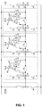
- Fig. 1 shows simplified and schematically a bus system according to the invention.
- the bus master signals to all auto-addressing bus nodes that the bus node addresses should be assigned.
- the following address assignment is split into address allocation phases, wherein in each address assignment phase exactly by means of an initialization run preferred exactly one Autoadressier bus node, namely the last of the Autoadressier bus nodes (SL1, SL2, SI3) from the bus master (ECU) in the bus node chain, which has no Bus node address receives a valid bus node address from the bus master (ECU) receives.
- the bus master transmits by means of a so-called broadcast command to all Autoadressier bus node the number of standard bus nodes that are before the Autoadressier bus node (SI1, SI2, SI3), ie between these and the bus master (ECU) or a maximum addressing current level.
- this maximum addressing current level I amax can also be programmed into the bus node since the bus topology is typically constructive and not operational and therefore predictable.
- I ref sum current
- the bus master (ECU) closes its switch (SB) again for a predetermined addressing time T A.
- this current sink (SB) of the bus master (ECU) is actually a more complex structure, which can also detect a bus short-circuit and is only reproduced here in simplified form.
- the bus master (ECU) provides a current sink for the addressing current of the auto addressing power sources and the bus node ground currents of the bus nodes in the following address assignment phase.
- the autoaddressable auto addressing bus nodes (SL1), (SL2) and (SL3) register that the data bus is pulled to ground and open their respective switches S1 and S2.
- the auto address bus nodes (SL1, SI2, SI3) no longer feed bus node base current into the data bus.
- the auto address bus nodes determine the base current through the respective bus shunt resistor (R2) by measuring the voltage drop across that bus shunt resistor (R2). This voltage drop, for example, as an offset voltage value in a sample-and-hold circuit between are stored and subtracted by a subtractor circuit in the sequence from the voltage drop then measured later via the bus shunt resistor (R2). This ensures that only the bus current deviating from the respective base current is used for the address assignment and the regulation of the addressing current sources (Iq1, Iq2, Iq3).
- This phase is ended after a second period of time has passed (dt2).
- All Autoadressier bus nodes that do not yet have a valid bus node address, detect the current differing from the base current through their respective bus shunt resistor (R2) and then regulate based on this Busstrommesswerts thus their respective addressing current source (Iq1, Iq2, Iq3 ) such that the current through its respective bus shunt resistor (R2) corresponds to the previously determined or predetermined current sum (I ref ).
- the respective auto addressing bus node has measuring means (R2, D1, D3) in order to determine the real current sum in the form of the respective bus node output current (i1, i2, i3) in the direction of the bus master (ECU).
- the voltage drop across the bus shunt resistor (R2) is detected and preferably further processed after subtracting the voltage value for the bus base current as current summation signal.
- the current summation signal thus generated is filtered in a preferably non-linear filter (F1) to form a control signal.
- This is compared with a reference value (Ref) by a differential amplifier stage, which equates to a comparison of the respective bus node output current (i1, i2, i3) with a reference current (I ref ) in its effect.
- this reference value (Ref) is therefore typically defined. This comparison can be done before and after the filtering in the filter (F).
- control value (rw1, rw2, rw3) thus determined then controls the respective addressing current source (Iq1, Iq2, Iq3) of the respective auto-addressing bus node (SL1, SL2, SL3).
- each bus node (SL1, SL2, SL3) can compare this control value (rwl, rw2, rw3) with a preferably approximately equal threshold value (SW).
- the end of this addressing phase is preferably characterized by the opening of the current sink switch (SB).
- SB current sink switch
- the bus nodes (SL1, SL2, SL3) then preferentially freeze the status of their respective control value (rw1, rw2, rw3) and evaluate it in comparison to the said threshold value (SW) and then decide on this basis whether they are the last autoaddresser.
- this auto-addressing bus node (SL3) no longer participates. This means that this auto-addressing bus node (SL3) then no longer feeds addressing current into the data bus by means of its addressing current source (Iq3).
- Iq3 addressing current source
- the bus node address of a car addressing bus node becomes invalid, e.g. at a voltage drop of the operating voltage below an operating voltage threshold or, for example, due to your command of the bus master or due to another signaling.
- the bus master checks the successful address assignment at the end of each initialization pass.
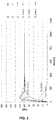
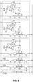
- Fig. 2 shows the course of the output current (i1) of the first bus node (SL1), the output current (i2) of the second bus node (SL2) and the output current (i3) of the third bus node (SL3). It also shows the current (I1-intern) of the addressing current source (Iq1) of the first bus node (SL1), the current (I2_intern) of the addressing current source (Iq2) of the second bus node (SL2) and the current (I3_intern) of the addressing current source (Iq3) of the third bus node (SL3).
- the time constants for up-regulation of the addressing current sources and down-regulation of the addressing current sources are approximately equal. It comes to an overshoot.
- the current (I1-intern) of the addressing current source (Iq1) of the first bus node (SL1) and the current (I2_intern) of the addressing current source (Iq2) of the second bus node (SL2) are controlled down by the controllers of these auto-addressing bus nodes while the current (I3_intern) of the addressing current source (Iq3) of the third bus node (SL3) is regulated to the reference value.
- the time to settle will be different than in the DE-B-10 2010 026 431 determined only by the first time constant ( ⁇ 1 ).
- Fig. 3 shows the course of the output current (i1) of the first bus node (SL1), the output current (i2) of the second bus node (SL2) and the output current (i3) of the third bus node (SL3). It also shows the current (I1_intern) of the addressing power source (Iq1) of the first bus node (SL1), the current (I2_intern) of the addressing power source (Iq2) of the second bus node (SL2) and the current (I3_intern) of the addressing power source (Iq3) of the third bus node (SL3).
- the time constants for up-regulation of the addressing current sources are about ten times as long as the time constants for the down-regulation of the addressing current sources. There is a minimal overshoot.
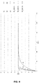
- Fig. 4 shows the course of the output current (i1) of the first bus node (SL1), the output current (i2) of the second bus node (SL2) and the output current (i3) of the third bus node (SL3). It also shows the current (I1_intern) of the addressing power source (Iq1) of the first bus node (SL1), the current (I2_intern) of the addressing power source (Iq2) of the second bus node (SL2) and the current (I3_intern) of the addressing power source (Iq3) of the third bus node (SL3).
- the time constants for up-regulation of the addressing current sources are about one hundred times as long as the time constants for the down-regulation of the addressing current sources. There is no overshoot.
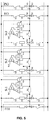
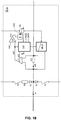
- Fig. 5 schematically shows a simplified Category A bus system with two standard bus nodes (CS1, CS2), which have no Autoaddress réellesever.
- Fig. 6 schematically shows a simplified Category B bus system with two standard bus nodes (CS1, CS2), which have no Autoaddress réellesever.
- Fig. 7 schematically shows a simplified Category C bus system with two standard bus nodes (CS1, CS2), which have no Autoaddress réellesever.
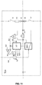
- Fig. 8 shows the case of the rotation of the second bus node (SL2).
- the LIN bus input and the LIN bus output are interchanged in this example.
- This operating case should be recognized.
- the interchange results in the bus shunt current (i2R) being fed through the bus shunt resistor (R2) of this twisted second bus node (SL2), in whose bus shunt resistor (R2) is fed backwards compared to the normal position.
- This bus shunt current (i2R) through the bus shunt resistor (R2) in this example comprises only the bus node output current (i3) of the subsequent, third auto-addressing bus node (SL3) or in other cases the subsequent bus node.
- This bus node output current (i3) of the third auto-addressing bus node (SL3) thus leads to a negative voltage drop (V R2 ) via the bus shunt resistor (R2).
- V R2 negative voltage drop
- Its output (ds1) saturates due to the negative drive by the negative voltage drop (V R2 ) via the bus shunt resistor (R2) at the smallest possible output level of the output (ds1) of the differential amplifier (D1).
- This smallest possible output level of the output (ds1) of the differential amplifier (D1) may be an absolute maximum value of a negative output value or an absolute minimum value of a positive output value.
- the output (ds1) of the first differential amplifier (D1) is typically below the level of the reference value (Ref).
- This causes a large positive signal at the output (ds3) of the third differential amplifier (D3) and thus at least after the settling of the non-linear filter (F) of the twisted auto-addressing bus node (SL2), maximizing the addressing current through the regulated addressing current source (iq2) of the second , here in this example error case twisted car addressing bus node (SL2).
- the control loop increases the addressing current which is fed into the data bus by the addressing current source (Iq2).
- the skewed second auto address bus node (SL2) may be determined from the voltage drop (V R2 ) across its bus shunt resistor (R2) which is the voltage magnitude of
- an xth auto address bus node (SLx) at an xth position in the chain of bus nodes will sense a negative voltage drop (V R2 ) across its bus shunt resistor (R2) and its addressing current source (Iq2) should receive a positive current supply, then the respective Autoadressier bus node (SL2) can recognize this constellation and initiate countermeasures.
- the xth auto addressing bus node turns off its addressing power source (Iqx) and takes a predetermined fault address as the bus node address.
- the bus master (ECU) can send a test query of the bus node with this error address as a bus node address after auto-addressing, whereupon they respond with a standardized response.
- the bus master (ECU) can then signal a bus error to all bus nodes and / or users in the simplest case. However, the bus master (ECU) can also issue a command to the bus nodes with this error address, whereupon, firstly, this is the entry point of your addressing stream, e.g. by a multiplexer (MUX) and, secondly, to change the polarity of the inputs or, alternatively, the output of the first differential amplifier (D1).
- MUX multiplexer
- D1 the output of the first differential amplifier
- the bus master (ECU) then carries out a new address assignment. Only if this is still faulty, he prefers to signal an error. Possibly. he switches off the then still affected bus node by command (broadcast command) to the said error address, since then obviously there is another error.
- the detection device changes the feed point for the addressing current source of the regulated addressing current source (Iqx) of the xth auto-address bus node (SLx), for example by means of an analog multiplexer (MUX) and reverses the polarity of the inputs or the output of the first differential amplifier ( D1) by means of the polarity signal (pol).
- MUX analog multiplexer
- a Umparametritation internal sub-devices such as current sources to neutralize the error possible if instead of an addressing current source (Iqx) of the xth Auto Addressing Bus node (SLx) and a multiplexer (MUX) a first addressing current source (Iqx1) of the xth Autoadressier bus node ( SLx) and, for example, a second addressing current source (Iqx2) of the xth auto-addressing bus node (SLx), of which the first addressing current source (Iqx1) of the xth auto-addressing bus node (SLx) feeds its addressing current before the bus shunt resistor (R2) and the second addressing current source (Iqx2 ) of the xth auto address bus node (SLx) feeds its addressing current behind the bus shunt resistor (R2).
- Iqx addressing current source
- MUX multiplexer
- the detection device would set the addressing current of one of the two current sources (Iqx1, Iqx2) to zero, so that the equivalent effect as with the combination of an addressing current source (Iqx) of the xth auto-address bus node (SLx) with the Switching by a multiplexer (MUX) is achieved.
- the detection device (DET) can recognize that the control value (rwx) of the xth auto address bus node (SLx) maximizes the addressing current of the addressing current source (iqx). This can be done, for example, with a suitable design by comparing the control value (rwx) with a second threshold (Ref2). If the derivative of the addressing current of the auto-addressing current source (iqx) after the control value (rwx) is positive, this means that the control value (rwx) is above the second threshold value (Ref2). Furthermore, the detection device (DET) can simultaneously compare the output (ds1) of the first differential amplifier (D1) with a third reference value.
- the detection device can conclude a negative voltage drop (V R2 ) via the bus shunt resistor (R2) or a voltage drop (V R2 ) close to zero via the bus shunt resistor (R2). This condition is illegal because the auto-addressing power source provides a positive addressing current which, when properly mounted, would have to flow through the bus shunt resistor (R2), but apparently this does not happen.
- Such a detected error the detection device (DET) for example via an error signal (he) signal to a bus node internal computer or a suitable controller.
- Fig. 11 shows the interconnection of the hardware for driving the Autoaddress istsstrom provoke (Iqx) and the feeding of Autoadress réellesstroms in the data bus when the bus node (SLx) against the interconnection in accordance with Fig. 10 "twisted" is integrated into the data bus.
- MUX multiplexer
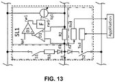
- Fig. 13 shows an addressing bus node (SL1), in which the components belonging to the transceiver are surrounded by dotted lines.
- the signal (RxD) is diverted from the bus and fed after processing the actual application (for example, a window or a seat adjustment), which in turn sends signals to the transceiver, which are then used as control signals (TxD) to control the transceiver.
- the segmented part of the bus node (SL1) which deals with the autoaddressing possibility and the feeding of the auto addressing current according to the invention into the data bus, is punctuated in dotted lines.
Landscapes
- Engineering & Computer Science (AREA)
- Computer Networks & Wireless Communication (AREA)
- Signal Processing (AREA)
- Theoretical Computer Science (AREA)
- Physics & Mathematics (AREA)
- General Physics & Mathematics (AREA)
- General Engineering & Computer Science (AREA)
- Quality & Reliability (AREA)
- Small-Scale Networks (AREA)
- Bus Control (AREA)
- Dc Digital Transmission (AREA)
- Tests Of Electronic Circuits (AREA)
- Debugging And Monitoring (AREA)
Applications Claiming Priority (2)
| Application Number | Priority Date | Filing Date | Title |
|---|---|---|---|
| DE102017122364 | 2017-09-26 | ||
| EP17210851.6A EP3461068B1 (fr) | 2017-09-26 | 2017-12-28 | Procédé d'attribution d'adresses dans un système de bus de données série et noeuds de bus pour un tel système de bus de données série |
Publications (2)
| Publication Number | Publication Date |
|---|---|
| EP3461069A1 true EP3461069A1 (fr) | 2019-03-27 |
| EP3461069B1 EP3461069B1 (fr) | 2021-09-01 |
Family
ID=60937576
Family Applications (2)
| Application Number | Title | Priority Date | Filing Date |
|---|---|---|---|
| EP17210851.6A Active EP3461068B1 (fr) | 2017-09-26 | 2017-12-28 | Procédé d'attribution d'adresses dans un système de bus de données série et noeuds de bus pour un tel système de bus de données série |
| EP18196807.4A Active EP3461069B1 (fr) | 2017-09-26 | 2018-09-26 | Procédé d'attribution d'adresses dans un système de bus de données série et noeuds de bus pour un tel système de bus de données série |
Family Applications Before (1)
| Application Number | Title | Priority Date | Filing Date |
|---|---|---|---|
| EP17210851.6A Active EP3461068B1 (fr) | 2017-09-26 | 2017-12-28 | Procédé d'attribution d'adresses dans un système de bus de données série et noeuds de bus pour un tel système de bus de données série |
Country Status (4)
| Country | Link |
|---|---|
| US (1) | US10311011B2 (fr) |
| EP (2) | EP3461068B1 (fr) |
| CN (2) | CN109862128B (fr) |
| DE (3) | DE102017128489B4 (fr) |
Cited By (4)
| Publication number | Priority date | Publication date | Assignee | Title |
|---|---|---|---|---|
| EP3703344A1 (fr) | 2019-02-27 | 2020-09-02 | ELMOS Semiconductor AG | Procédé de création de la possibilité de vérification de l'exactitude d'adresses attribuées précédemment aux noeuds de bus d'un système de bus de données sériel |
| CN113495853A (zh) * | 2020-03-19 | 2021-10-12 | 施耐德电器工业公司 | 为总线参与者分配地址的方法 |
| CN119276838A (zh) * | 2024-11-26 | 2025-01-07 | 上海朔集半导体科技有限公司 | 地址分配方法及装置、计算机可读存储介质、通信系统 |
| CN119299429A (zh) * | 2024-11-26 | 2025-01-10 | 上海朔集半导体科技有限公司 | 从节点地址分配方法及装置、可读存储介质、通信系统 |
Families Citing this family (14)
| Publication number | Priority date | Publication date | Assignee | Title |
|---|---|---|---|---|
| CN111431596B (zh) * | 2020-03-24 | 2021-04-02 | 中星联华科技(北京)有限公司 | 一种信号升速方法及电路 |
| DE102020113332A1 (de) | 2020-05-18 | 2021-11-18 | Elmos Semiconductor Se | Abwärtskompatibles Bussystem mit niedrigem Buswiderstand mit der Fähigkeit zur Vergabe der Busknotenadressen mittels AMR- oder GMR Messmitteln |
| DE112021006722A5 (de) * | 2020-12-29 | 2023-10-26 | Elmos Semiconductor Se | Teilnehmer für ein Kommunikationsbussystem, Kommunikationsbussystem mit derartigen Teilnehmern und Verfahren zum Signalisieren defekter Teilnehmer sowie zur Autoadressierung intakter Teilnehmer |
| CN117354281B (zh) * | 2022-06-29 | 2024-10-29 | 比亚迪股份有限公司 | 基于lin通信的执行器标识码的配置方法及车辆控制器 |
| CN115230578A (zh) * | 2022-07-27 | 2022-10-25 | 浙江吉利控股集团有限公司 | 车辆的节点地址分配方法、装置、车辆设备及存储介质 |
| CN115086278B (zh) * | 2022-08-19 | 2022-10-28 | 上海泰矽微电子有限公司 | 一种lin总线系统及其从机自动寻址的方法 |
| EP4376364B1 (fr) * | 2022-11-22 | 2026-01-07 | Nxp B.V. | Émetteur-récepteur can et procédé pour l'émetteur-récepteur can |
| CN116527431A (zh) * | 2023-03-31 | 2023-08-01 | 上海矽力杰微电子技术有限公司 | 一种单线通信方法以及系统 |
| CN117135142B (zh) * | 2023-10-26 | 2024-02-06 | 浙江大学 | 电动汽车电机柔性生产线性能测试的地址分配装置及方法 |
| CN117714418B (zh) * | 2023-12-20 | 2024-06-11 | 武汉芯必达微电子有限公司 | 一种基于电源监控的lin网络自动寻址系统及其实现方法 |
| DE102024107988B3 (de) * | 2024-03-20 | 2025-07-17 | Elmos Semiconductor Se | Vorrichtung zur Detektion eines Adressierstroms in einer Busshunt-Konfiguration eines Teilnehmers eines Kommunikationsbussystems in einer Adressvergabephase |
| CN118611665B (zh) * | 2024-08-08 | 2024-10-29 | 江苏帝奥微电子股份有限公司 | 一种lin自动寻址的修调系统及其方法 |
| CN118964225B (zh) * | 2024-10-12 | 2025-03-11 | 无锡英迪芯微电子科技股份有限公司 | 一种自动寻址方法及系统 |
| CN119561800B (zh) * | 2025-01-24 | 2025-05-09 | 江苏云途半导体有限公司 | 一种基于bsm的lin从节点及lin自动寻址方法 |
Citations (11)
| Publication number | Priority date | Publication date | Assignee | Title |
|---|---|---|---|---|
| DE10256631A1 (de) * | 2002-12-03 | 2004-07-01 | Elmos Semiconductor Ag | Verfarhen zur Adressierung der Teilnehmer eines Bussystems |
| DE10147512B4 (de) | 2001-09-26 | 2004-08-26 | Elmos Semiconductor Ag | Verfahren zur Adressierung der Teilnehmer eines Bussystems |
| EP1490772B1 (fr) | 2002-05-02 | 2005-06-01 | ELMOS Semiconductor AG | Procede d'adressage de dispositifs utilisateurs d'un systeme a bus au moyen de courants d'identification |
| WO2005050924A1 (fr) | 2003-10-24 | 2005-06-02 | Elmos Semiconductor Ag | Procede d'attribution d'adresses en serie et de controle de l'attribution d'adresses dans un systeme de bus |
| EP1298851B1 (fr) | 2001-09-26 | 2007-05-30 | ELMOS Semiconductor AG | Procédé d'adressage de noeuds d'un système de bus |
| EP1603282B1 (fr) | 2004-06-03 | 2008-09-24 | ELMOS Semiconductor AG | Procédé d'adressage des abonnés d'un système de bus |
| US7590140B2 (en) | 2004-06-08 | 2009-09-15 | Elmos Semiconductor Ag | Method for addressing the participants of a bus system |
| DE102010026431A1 (de) | 2010-07-06 | 2012-01-12 | Jörg Hartzsch | Verfahren zur Adresszuteilung an Teilnehmer eines Bussystems |
| EP2571200A2 (fr) | 2011-09-16 | 2013-03-20 | Nxp B.V. | Circuit de communication de réseau, système et procédé |
| EP2654246A2 (fr) | 2012-04-20 | 2013-10-23 | Nxp B.V. | Appareil, système et procédé de communication de réseau |
| US9558140B2 (en) | 2012-10-02 | 2017-01-31 | Melexis Technologies N.V. | Method for addressing the participants of a bus system |
Family Cites Families (12)
| Publication number | Priority date | Publication date | Assignee | Title |
|---|---|---|---|---|
| US5831546A (en) | 1996-05-10 | 1998-11-03 | General Signal Corporation | Automatic addressing in life safety system |
| US7565470B2 (en) * | 2007-12-04 | 2009-07-21 | Holylite Microelectronics Corp. | Serial bus device with address assignment by master device |
| DE102008017281A1 (de) * | 2008-04-04 | 2009-10-08 | Zumtobel Lighting Gmbh | Automatische Busadressvergabe mittels Kollisionsprüfung |
| US8122159B2 (en) * | 2009-01-16 | 2012-02-21 | Allegro Microsystems, Inc. | Determining addresses of electrical components arranged in a daisy chain |
| US9399755B2 (en) * | 2010-05-11 | 2016-07-26 | Pall Artelis | Apparatus and methods for cell culture |
| US8775689B2 (en) * | 2011-05-02 | 2014-07-08 | Deere & Company | Electronic modules with automatic configuration |
| US8645580B2 (en) * | 2011-09-06 | 2014-02-04 | Semiconductor Components Industries, Llc | Circuit and electronic module for automatic addressing |
| US9160559B2 (en) * | 2012-05-16 | 2015-10-13 | Infineon Technologies, Ag | System and method to address devices connected to a bus system |
| DE102013201106B4 (de) * | 2013-01-24 | 2014-12-11 | Smiths Heimann Gmbh | Busknoten und Bussystem sowie Verfahren zur Identifikation der Busknoten des Bussystems |
| CN105718414A (zh) * | 2016-01-19 | 2016-06-29 | 圣邦微电子(北京)股份有限公司 | 一种可寻址的总线结构 |
| ES2925737T3 (es) * | 2016-01-29 | 2022-10-19 | Form Energy Inc | Direccionamiento automático de nodos de batería en un sistema de batería |
| US10715350B2 (en) * | 2016-09-19 | 2020-07-14 | Simmonds Precision Products, Inc. | Automatic addressing of networked nodes |
-
2017
- 2017-11-30 DE DE102017128489.3A patent/DE102017128489B4/de active Active
- 2017-12-05 DE DE102017128923.2A patent/DE102017128923A1/de active Pending
- 2017-12-28 EP EP17210851.6A patent/EP3461068B1/fr active Active
-
2018
- 2018-02-27 DE DE102018104488.7A patent/DE102018104488A1/de active Pending
- 2018-09-21 US US16/137,561 patent/US10311011B2/en active Active
- 2018-09-26 CN CN201811126184.0A patent/CN109862128B/zh active Active
- 2018-09-26 EP EP18196807.4A patent/EP3461069B1/fr active Active
- 2018-09-26 CN CN201811126287.7A patent/CN109618013B/zh active Active
Patent Citations (14)
| Publication number | Priority date | Publication date | Assignee | Title |
|---|---|---|---|---|
| EP1298851B1 (fr) | 2001-09-26 | 2007-05-30 | ELMOS Semiconductor AG | Procédé d'adressage de noeuds d'un système de bus |
| DE10147512B4 (de) | 2001-09-26 | 2004-08-26 | Elmos Semiconductor Ag | Verfahren zur Adressierung der Teilnehmer eines Bussystems |
| EP1490772B1 (fr) | 2002-05-02 | 2005-06-01 | ELMOS Semiconductor AG | Procede d'adressage de dispositifs utilisateurs d'un systeme a bus au moyen de courants d'identification |
| US20050132109A1 (en) | 2002-05-02 | 2005-06-16 | Elmos Semiconductor Ag | Method for addressing the users of a bus system by means of identification flows |
| DE10256631A1 (de) * | 2002-12-03 | 2004-07-01 | Elmos Semiconductor Ag | Verfarhen zur Adressierung der Teilnehmer eines Bussystems |
| DE10256631B4 (de) | 2002-12-03 | 2005-07-14 | Elmos Semiconductor Ag | Verfarhen zur Adressierung der Teilnehmer eines Bussystems |
| WO2005050924A1 (fr) | 2003-10-24 | 2005-06-02 | Elmos Semiconductor Ag | Procede d'attribution d'adresses en serie et de controle de l'attribution d'adresses dans un systeme de bus |
| EP1603282B1 (fr) | 2004-06-03 | 2008-09-24 | ELMOS Semiconductor AG | Procédé d'adressage des abonnés d'un système de bus |
| US7590140B2 (en) | 2004-06-08 | 2009-09-15 | Elmos Semiconductor Ag | Method for addressing the participants of a bus system |
| DE102010026431A1 (de) | 2010-07-06 | 2012-01-12 | Jörg Hartzsch | Verfahren zur Adresszuteilung an Teilnehmer eines Bussystems |
| EP2571200A2 (fr) | 2011-09-16 | 2013-03-20 | Nxp B.V. | Circuit de communication de réseau, système et procédé |
| EP2654246A2 (fr) | 2012-04-20 | 2013-10-23 | Nxp B.V. | Appareil, système et procédé de communication de réseau |
| US9331866B2 (en) | 2012-04-20 | 2016-05-03 | Nxp B.V. | Network communications apparatus, system, and method |
| US9558140B2 (en) | 2012-10-02 | 2017-01-31 | Melexis Technologies N.V. | Method for addressing the participants of a bus system |
Cited By (6)
| Publication number | Priority date | Publication date | Assignee | Title |
|---|---|---|---|---|
| EP3703344A1 (fr) | 2019-02-27 | 2020-09-02 | ELMOS Semiconductor AG | Procédé de création de la possibilité de vérification de l'exactitude d'adresses attribuées précédemment aux noeuds de bus d'un système de bus de données sériel |
| US11038712B2 (en) | 2019-02-27 | 2021-06-15 | Elmos Semiconductor Ag | Bus node address verification |
| CN113495853A (zh) * | 2020-03-19 | 2021-10-12 | 施耐德电器工业公司 | 为总线参与者分配地址的方法 |
| US11782862B2 (en) | 2020-03-19 | 2023-10-10 | Schneider Electric Industries Sas | Method of assigning addresses to bus participants |
| CN119276838A (zh) * | 2024-11-26 | 2025-01-07 | 上海朔集半导体科技有限公司 | 地址分配方法及装置、计算机可读存储介质、通信系统 |
| CN119299429A (zh) * | 2024-11-26 | 2025-01-10 | 上海朔集半导体科技有限公司 | 从节点地址分配方法及装置、可读存储介质、通信系统 |
Also Published As
| Publication number | Publication date |
|---|---|
| EP3461069B1 (fr) | 2021-09-01 |
| DE102017128489B4 (de) | 2025-08-14 |
| EP3461068B1 (fr) | 2021-06-30 |
| DE102018104488A1 (de) | 2019-03-28 |
| US20190095379A1 (en) | 2019-03-28 |
| CN109618013A (zh) | 2019-04-12 |
| DE102017128923A1 (de) | 2019-03-28 |
| DE102017128489A1 (de) | 2019-03-28 |
| CN109862128A (zh) | 2019-06-07 |
| CN109862128B (zh) | 2023-07-25 |
| US10311011B2 (en) | 2019-06-04 |
| EP3461068A1 (fr) | 2019-03-27 |
| CN109618013B (zh) | 2023-05-12 |
Similar Documents
| Publication | Publication Date | Title |
|---|---|---|
| EP3461069B1 (fr) | Procédé d'attribution d'adresses dans un système de bus de données série et noeuds de bus pour un tel système de bus de données série | |
| EP3493481B1 (fr) | Procédé d'alimentation de flux d'adressage au moyen des n uds de bus d'un système de bus de données série et n uds de bus pour un tel système de bus de données | |
| DE102017122365B3 (de) | Selbsttestfähiges Bussystem und Verwendung dieser Selbsttestfähigkeit zur Vergabe von Busknotenadressen | |
| EP3496341B1 (fr) | Procédé de commande d'un système de base de données série et noeuds de bus pour un tel système de base de données | |
| DE102018104489A1 (de) | Selbsttestfähiges Bussystem und Verwendung dieser Selbsttestfähigkeit zur Vergabe von Busknotenadressen mit Mischverbaumöglichkeit | |
| EP1490772B1 (fr) | Procede d'adressage de dispositifs utilisateurs d'un systeme a bus au moyen de courants d'identification | |
| EP3759872B1 (fr) | Procédé et dispositif de commande de composants électriques et/ou électroniques d'un module de véhicule à moteur | |
| DE19725710A1 (de) | Verfahren und Vorrichtung zur Leistungs- und Datenübermittlung auf gemeinsamen Leitungen | |
| DE102017012179B4 (de) | Selbsttestfähiges Bussystem und Verwendung dieser Selbsttestfähigkeit zur Vergabe von Busknotenadressen | |
| DE102018104852A1 (de) | Verfahren zur Ansteuerung elektrischer und/oder elektronischer Komponenten eines Kfz-Moduls und ein derartiges Kfz-Modul mit automatischer Moduladressierung mittels Bus-Shunt-Widerständen in einem differenziellen Bus | |
| DE102018010267A1 (de) | Selbsttestfähiges Bussystem und Verwendung dieser Selbsttestfähigkeit zur Vergabe von Busknotenadressen mit Mischverbaumöglichkeit | |
| DE102018104873A1 (de) | Vorrichtung zur Ansteuerung elektrischer und/oder elektronischer Komponenten eines Kfz-Moduls und ein derartiges Kfz-Modul mit automatischer Moduladressierung über Powerline | |
| DE102019104787A1 (de) | Selbsttestfähiges Bussystem und Verwendung dieser Selbsttestfähigkeit zur Vergabe von Busknotenadressen mit Mischverbaumöglichkeit | |
| DE102018124279A1 (de) | Abwärtskompatibles Bussystem mit niedrigem Buswiderstand mit der Fähigkeit zur Vergabe der Busknotenadressen ohne oder mit niederohmigen Bus-Shunt | |
| EP3893607B1 (fr) | Procédé d'adressage local précis des utilisateurs de bus dans un système de bus de données différentiel bifilaire et système de bus de données différentiel bifilaire | |
| DE102018104850A1 (de) | Vorrichtung zur Ansteuerung elektrischer und/oder elektronischer Komponenten eines Kfz-Moduls und ein derartiges Kfz-Modul mit automatischer Moduladressierung mit Verifikation | |
| DE10153847C2 (de) | Verfahren zur Identifizierung von baugleichen Elektronikmodulen in einer CAN-Busarchitektur und geeignetes Elektronikmodul | |
| DE102018104872A1 (de) | Verfahren zur Ansteuerung elektrischer und/oder elektronischer Komponenten eines Kfz-Moduls und ein derartiges Kfz-Modul mit automatischer Moduladressierung über Powerline | |
| DE102018104862B4 (de) | Vorrichtung zur Ansteuerung elektrischer und/oder elektronischer Komponenten eines Kfz-Moduls und ein derartiges Kfz-Modul mit automatischer Moduladressierung und Bus-Shunt-Überbrückungsschaltern | |
| DE102018104858A1 (de) | Vorrichtung zur Ansteuerung elektrischer und/oder elektronischer Komponenten eines Kfz-Moduls und ein derartiges Kfz-Modul mit automatischer Moduladressierung über eine Interruptleitung | |
| DE102018104855A1 (de) | Verfahren zur Ansteuerung elektrischer und/oder elektronischer Komponenten eines Kfz-Moduls und ein derartiges Kfz-Modul mit automatischer Moduladressierung mittels differenziellen Bus-Shunt-Widerständen | |
| DE102018104871A1 (de) | Vorrichtung zur Ansteuerung elektrischer und/oder elektronischer Komponenten eines Kfz-Moduls und ein derartiges Kfz-Modul mit automatischer Moduladressierung mittels Gleichtakt- oder Gegentaktstromquellen | |
| DE102018104868A1 (de) | Vorrichtung zur Ansteuerung elektrischer und/oder elektronischer Komponenten eines Kfz-Moduls und ein derartiges Kfz-Modul mit automatischer Moduladressierung mittels eines Bus-Shunt-Widerstands | |
| DE102018104847A1 (de) | Verfahren zur Ansteuerung elektrischer und/oder elektronischer Komponenten eines Kfz-Moduls und ein derartiges Kfz-Modul mit automatischer Moduladressierung mittels Daisy-Chain | |
| DE102019120210A1 (de) | Abwärtskompatibles Bussystem mit niedrigem Buswiderstand mit der Fähigkeit zur Vergabe der Busknotenadressen ohne oder mit niederohmigen Bus-Shunt mittels zumindest zeitweise zeitlich konstanten Magnetfeldern |
Legal Events
| Date | Code | Title | Description |
|---|---|---|---|
| PUAI | Public reference made under article 153(3) epc to a published international application that has entered the european phase |
Free format text: ORIGINAL CODE: 0009012 |
|
| STAA | Information on the status of an ep patent application or granted ep patent |
Free format text: STATUS: THE APPLICATION HAS BEEN PUBLISHED |
|
| AK | Designated contracting states |
Kind code of ref document: A1 Designated state(s): AL AT BE BG CH CY CZ DE DK EE ES FI FR GB GR HR HU IE IS IT LI LT LU LV MC MK MT NL NO PL PT RO RS SE SI SK SM TR |
|
| AX | Request for extension of the european patent |
Extension state: BA ME |
|
| STAA | Information on the status of an ep patent application or granted ep patent |
Free format text: STATUS: REQUEST FOR EXAMINATION WAS MADE |
|
| 17P | Request for examination filed |
Effective date: 20190926 |
|
| RBV | Designated contracting states (corrected) |
Designated state(s): AL AT BE BG CH CY CZ DE DK EE ES FI FR GB GR HR HU IE IS IT LI LT LU LV MC MK MT NL NO PL PT RO RS SE SI SK SM TR |
|
| RAP1 | Party data changed (applicant data changed or rights of an application transferred) |
Owner name: ELMOS SEMICONDUCTOR SE |
|
| GRAP | Despatch of communication of intention to grant a patent |
Free format text: ORIGINAL CODE: EPIDOSNIGR1 |
|
| STAA | Information on the status of an ep patent application or granted ep patent |
Free format text: STATUS: GRANT OF PATENT IS INTENDED |
|
| RIC1 | Information provided on ipc code assigned before grant |
Ipc: H04L 12/403 20060101AFI20201009BHEP Ipc: G05B 19/00 20060101ALI20201009BHEP Ipc: H04L 29/12 20060101ALI20201009BHEP Ipc: H04L 12/40 20060101ALI20201009BHEP Ipc: G06F 13/42 20060101ALI20201009BHEP |
|
| INTG | Intention to grant announced |
Effective date: 20201109 |
|
| RIN1 | Information on inventor provided before grant (corrected) |
Inventor name: SCHMITZ, CHRISTIAN Inventor name: BURCHARD, BERND |
|
| GRAJ | Information related to disapproval of communication of intention to grant by the applicant or resumption of examination proceedings by the epo deleted |
Free format text: ORIGINAL CODE: EPIDOSDIGR1 |
|
| STAA | Information on the status of an ep patent application or granted ep patent |
Free format text: STATUS: REQUEST FOR EXAMINATION WAS MADE |
|
| INTC | Intention to grant announced (deleted) | ||
| GRAS | Grant fee paid |
Free format text: ORIGINAL CODE: EPIDOSNIGR3 |
|
| STAA | Information on the status of an ep patent application or granted ep patent |
Free format text: STATUS: GRANT OF PATENT IS INTENDED |
|
| GRAP | Despatch of communication of intention to grant a patent |
Free format text: ORIGINAL CODE: EPIDOSNIGR1 |
|
| INTG | Intention to grant announced |
Effective date: 20210507 |
|
| GRAA | (expected) grant |
Free format text: ORIGINAL CODE: 0009210 |
|
| STAA | Information on the status of an ep patent application or granted ep patent |
Free format text: STATUS: THE PATENT HAS BEEN GRANTED |
|
| AK | Designated contracting states |
Kind code of ref document: B1 Designated state(s): AL AT BE BG CH CY CZ DE DK EE ES FI FR GB GR HR HU IE IS IT LI LT LU LV MC MK MT NL NO PL PT RO RS SE SI SK SM TR |
|
| REG | Reference to a national code |
Ref country code: GB Ref legal event code: FG4D Free format text: NOT ENGLISH |
|
| REG | Reference to a national code |
Ref country code: CH Ref legal event code: EP Ref country code: AT Ref legal event code: REF Ref document number: 1427404 Country of ref document: AT Kind code of ref document: T Effective date: 20210915 |
|
| REG | Reference to a national code |
Ref country code: DE Ref legal event code: R096 Ref document number: 502018006803 Country of ref document: DE |
|
| REG | Reference to a national code |
Ref country code: IE Ref legal event code: FG4D Free format text: LANGUAGE OF EP DOCUMENT: GERMAN |
|
| REG | Reference to a national code |
Ref country code: LT Ref legal event code: MG9D |
|
| REG | Reference to a national code |
Ref country code: NL Ref legal event code: MP Effective date: 20210901 |
|
| PG25 | Lapsed in a contracting state [announced via postgrant information from national office to epo] |
Ref country code: NO Free format text: LAPSE BECAUSE OF FAILURE TO SUBMIT A TRANSLATION OF THE DESCRIPTION OR TO PAY THE FEE WITHIN THE PRESCRIBED TIME-LIMIT Effective date: 20211201 Ref country code: BG Free format text: LAPSE BECAUSE OF FAILURE TO SUBMIT A TRANSLATION OF THE DESCRIPTION OR TO PAY THE FEE WITHIN THE PRESCRIBED TIME-LIMIT Effective date: 20211201 Ref country code: LT Free format text: LAPSE BECAUSE OF FAILURE TO SUBMIT A TRANSLATION OF THE DESCRIPTION OR TO PAY THE FEE WITHIN THE PRESCRIBED TIME-LIMIT Effective date: 20210901 Ref country code: ES Free format text: LAPSE BECAUSE OF FAILURE TO SUBMIT A TRANSLATION OF THE DESCRIPTION OR TO PAY THE FEE WITHIN THE PRESCRIBED TIME-LIMIT Effective date: 20210901 Ref country code: FI Free format text: LAPSE BECAUSE OF FAILURE TO SUBMIT A TRANSLATION OF THE DESCRIPTION OR TO PAY THE FEE WITHIN THE PRESCRIBED TIME-LIMIT Effective date: 20210901 Ref country code: HR Free format text: LAPSE BECAUSE OF FAILURE TO SUBMIT A TRANSLATION OF THE DESCRIPTION OR TO PAY THE FEE WITHIN THE PRESCRIBED TIME-LIMIT Effective date: 20210901 Ref country code: SE Free format text: LAPSE BECAUSE OF FAILURE TO SUBMIT A TRANSLATION OF THE DESCRIPTION OR TO PAY THE FEE WITHIN THE PRESCRIBED TIME-LIMIT Effective date: 20210901 Ref country code: RS Free format text: LAPSE BECAUSE OF FAILURE TO SUBMIT A TRANSLATION OF THE DESCRIPTION OR TO PAY THE FEE WITHIN THE PRESCRIBED TIME-LIMIT Effective date: 20210901 |
|
| PG25 | Lapsed in a contracting state [announced via postgrant information from national office to epo] |
Ref country code: PL Free format text: LAPSE BECAUSE OF FAILURE TO SUBMIT A TRANSLATION OF THE DESCRIPTION OR TO PAY THE FEE WITHIN THE PRESCRIBED TIME-LIMIT Effective date: 20210901 Ref country code: LV Free format text: LAPSE BECAUSE OF FAILURE TO SUBMIT A TRANSLATION OF THE DESCRIPTION OR TO PAY THE FEE WITHIN THE PRESCRIBED TIME-LIMIT Effective date: 20210901 Ref country code: GR Free format text: LAPSE BECAUSE OF FAILURE TO SUBMIT A TRANSLATION OF THE DESCRIPTION OR TO PAY THE FEE WITHIN THE PRESCRIBED TIME-LIMIT Effective date: 20211202 |
|
| REG | Reference to a national code |
Ref country code: CH Ref legal event code: PL |
|
| REG | Reference to a national code |
Ref country code: BE Ref legal event code: MM Effective date: 20210930 |
|
| PG25 | Lapsed in a contracting state [announced via postgrant information from national office to epo] |
Ref country code: IS Free format text: LAPSE BECAUSE OF FAILURE TO SUBMIT A TRANSLATION OF THE DESCRIPTION OR TO PAY THE FEE WITHIN THE PRESCRIBED TIME-LIMIT Effective date: 20220101 Ref country code: SM Free format text: LAPSE BECAUSE OF FAILURE TO SUBMIT A TRANSLATION OF THE DESCRIPTION OR TO PAY THE FEE WITHIN THE PRESCRIBED TIME-LIMIT Effective date: 20210901 Ref country code: SK Free format text: LAPSE BECAUSE OF FAILURE TO SUBMIT A TRANSLATION OF THE DESCRIPTION OR TO PAY THE FEE WITHIN THE PRESCRIBED TIME-LIMIT Effective date: 20210901 Ref country code: RO Free format text: LAPSE BECAUSE OF FAILURE TO SUBMIT A TRANSLATION OF THE DESCRIPTION OR TO PAY THE FEE WITHIN THE PRESCRIBED TIME-LIMIT Effective date: 20210901 Ref country code: PT Free format text: LAPSE BECAUSE OF FAILURE TO SUBMIT A TRANSLATION OF THE DESCRIPTION OR TO PAY THE FEE WITHIN THE PRESCRIBED TIME-LIMIT Effective date: 20220103 Ref country code: NL Free format text: LAPSE BECAUSE OF FAILURE TO SUBMIT A TRANSLATION OF THE DESCRIPTION OR TO PAY THE FEE WITHIN THE PRESCRIBED TIME-LIMIT Effective date: 20210901 Ref country code: EE Free format text: LAPSE BECAUSE OF FAILURE TO SUBMIT A TRANSLATION OF THE DESCRIPTION OR TO PAY THE FEE WITHIN THE PRESCRIBED TIME-LIMIT Effective date: 20210901 Ref country code: CZ Free format text: LAPSE BECAUSE OF FAILURE TO SUBMIT A TRANSLATION OF THE DESCRIPTION OR TO PAY THE FEE WITHIN THE PRESCRIBED TIME-LIMIT Effective date: 20210901 Ref country code: AL Free format text: LAPSE BECAUSE OF FAILURE TO SUBMIT A TRANSLATION OF THE DESCRIPTION OR TO PAY THE FEE WITHIN THE PRESCRIBED TIME-LIMIT Effective date: 20210901 |
|
| REG | Reference to a national code |
Ref country code: DE Ref legal event code: R097 Ref document number: 502018006803 Country of ref document: DE |
|
| PG25 | Lapsed in a contracting state [announced via postgrant information from national office to epo] |
Ref country code: MC Free format text: LAPSE BECAUSE OF FAILURE TO SUBMIT A TRANSLATION OF THE DESCRIPTION OR TO PAY THE FEE WITHIN THE PRESCRIBED TIME-LIMIT Effective date: 20210901 |
|
| PLBE | No opposition filed within time limit |
Free format text: ORIGINAL CODE: 0009261 |
|
| STAA | Information on the status of an ep patent application or granted ep patent |
Free format text: STATUS: NO OPPOSITION FILED WITHIN TIME LIMIT |
|
| PG25 | Lapsed in a contracting state [announced via postgrant information from national office to epo] |
Ref country code: LU Free format text: LAPSE BECAUSE OF NON-PAYMENT OF DUE FEES Effective date: 20210926 Ref country code: IT Free format text: LAPSE BECAUSE OF FAILURE TO SUBMIT A TRANSLATION OF THE DESCRIPTION OR TO PAY THE FEE WITHIN THE PRESCRIBED TIME-LIMIT Effective date: 20210901 Ref country code: IE Free format text: LAPSE BECAUSE OF NON-PAYMENT OF DUE FEES Effective date: 20210926 Ref country code: DK Free format text: LAPSE BECAUSE OF FAILURE TO SUBMIT A TRANSLATION OF THE DESCRIPTION OR TO PAY THE FEE WITHIN THE PRESCRIBED TIME-LIMIT Effective date: 20210901 Ref country code: BE Free format text: LAPSE BECAUSE OF NON-PAYMENT OF DUE FEES Effective date: 20210930 |
|
| 26N | No opposition filed |
Effective date: 20220602 |
|
| PG25 | Lapsed in a contracting state [announced via postgrant information from national office to epo] |
Ref country code: SI Free format text: LAPSE BECAUSE OF FAILURE TO SUBMIT A TRANSLATION OF THE DESCRIPTION OR TO PAY THE FEE WITHIN THE PRESCRIBED TIME-LIMIT Effective date: 20210901 Ref country code: LI Free format text: LAPSE BECAUSE OF NON-PAYMENT OF DUE FEES Effective date: 20210930 Ref country code: CH Free format text: LAPSE BECAUSE OF NON-PAYMENT OF DUE FEES Effective date: 20210930 |
|
| GBPC | Gb: european patent ceased through non-payment of renewal fee |
Effective date: 20220926 |
|
| PG25 | Lapsed in a contracting state [announced via postgrant information from national office to epo] |
Ref country code: CY Free format text: LAPSE BECAUSE OF FAILURE TO SUBMIT A TRANSLATION OF THE DESCRIPTION OR TO PAY THE FEE WITHIN THE PRESCRIBED TIME-LIMIT Effective date: 20210901 |
|
| P01 | Opt-out of the competence of the unified patent court (upc) registered |
Effective date: 20230525 |
|
| PG25 | Lapsed in a contracting state [announced via postgrant information from national office to epo] |
Ref country code: HU Free format text: LAPSE BECAUSE OF FAILURE TO SUBMIT A TRANSLATION OF THE DESCRIPTION OR TO PAY THE FEE WITHIN THE PRESCRIBED TIME-LIMIT; INVALID AB INITIO Effective date: 20180926 |
|
| PG25 | Lapsed in a contracting state [announced via postgrant information from national office to epo] |
Ref country code: GB Free format text: LAPSE BECAUSE OF NON-PAYMENT OF DUE FEES Effective date: 20220926 |
|
| PG25 | Lapsed in a contracting state [announced via postgrant information from national office to epo] |
Ref country code: MK Free format text: LAPSE BECAUSE OF FAILURE TO SUBMIT A TRANSLATION OF THE DESCRIPTION OR TO PAY THE FEE WITHIN THE PRESCRIBED TIME-LIMIT Effective date: 20210901 |
|
| PG25 | Lapsed in a contracting state [announced via postgrant information from national office to epo] |
Ref country code: TR Free format text: LAPSE BECAUSE OF FAILURE TO SUBMIT A TRANSLATION OF THE DESCRIPTION OR TO PAY THE FEE WITHIN THE PRESCRIBED TIME-LIMIT Effective date: 20210901 |
|
| PG25 | Lapsed in a contracting state [announced via postgrant information from national office to epo] |
Ref country code: MT Free format text: LAPSE BECAUSE OF FAILURE TO SUBMIT A TRANSLATION OF THE DESCRIPTION OR TO PAY THE FEE WITHIN THE PRESCRIBED TIME-LIMIT Effective date: 20210901 |
|
| REG | Reference to a national code |
Ref country code: AT Ref legal event code: MM01 Ref document number: 1427404 Country of ref document: AT Kind code of ref document: T Effective date: 20230926 |
|
| PG25 | Lapsed in a contracting state [announced via postgrant information from national office to epo] |
Ref country code: AT Free format text: LAPSE BECAUSE OF NON-PAYMENT OF DUE FEES Effective date: 20230926 |
|
| PG25 | Lapsed in a contracting state [announced via postgrant information from national office to epo] |
Ref country code: AT Free format text: LAPSE BECAUSE OF NON-PAYMENT OF DUE FEES Effective date: 20230926 |
|
| PGFP | Annual fee paid to national office [announced via postgrant information from national office to epo] |
Ref country code: DE Payment date: 20250915 Year of fee payment: 8 |
|
| PGFP | Annual fee paid to national office [announced via postgrant information from national office to epo] |
Ref country code: FR Payment date: 20250924 Year of fee payment: 8 |
|
| REG | Reference to a national code |
Ref country code: DE Ref legal event code: R081 Ref document number: 502018006803 Country of ref document: DE Owner name: ELMOS SEMICONDUCTOR SE, DE Free format text: FORMER OWNER: ELMOS SEMICONDUCTOR SE, 44227 DORTMUND, DE |