EP3460952B1 - Spannungsgeregelter oszillator für grosssignale - Google Patents
Spannungsgeregelter oszillator für grosssignale Download PDFInfo
- Publication number
- EP3460952B1 EP3460952B1 EP18000769.2A EP18000769A EP3460952B1 EP 3460952 B1 EP3460952 B1 EP 3460952B1 EP 18000769 A EP18000769 A EP 18000769A EP 3460952 B1 EP3460952 B1 EP 3460952B1
- Authority
- EP
- European Patent Office
- Prior art keywords
- voltage
- frequency
- current
- resonant network
- coupling
- Prior art date
- Legal status (The legal status is an assumption and is not a legal conclusion. Google has not performed a legal analysis and makes no representation as to the accuracy of the status listed.)
- Active
Links
Images







Classifications
-
- H—ELECTRICITY
- H02—GENERATION; CONVERSION OR DISTRIBUTION OF ELECTRIC POWER
- H02J—ELECTRIC POWER NETWORKS; CIRCUIT ARRANGEMENTS OR SYSTEMS FOR SUPPLYING OR DISTRIBUTING ELECTRIC POWER; SYSTEMS FOR STORING ELECTRIC ENERGY
- H02J50/00—Circuit arrangements or systems for wireless supply or distribution of electric power
- H02J50/40—Circuit arrangements or systems for wireless supply or distribution of electric power using two or more transmitting or receiving devices
- H02J50/402—Circuit arrangements or systems for wireless supply or distribution of electric power using two or more transmitting or receiving devices the two or more transmitting or the two or more receiving devices being integrated in the same unit, e.g. power mats with several coils or antennas with several sub-antennas
-
- H—ELECTRICITY
- H02—GENERATION; CONVERSION OR DISTRIBUTION OF ELECTRIC POWER
- H02J—ELECTRIC POWER NETWORKS; CIRCUIT ARRANGEMENTS OR SYSTEMS FOR SUPPLYING OR DISTRIBUTING ELECTRIC POWER; SYSTEMS FOR STORING ELECTRIC ENERGY
- H02J50/00—Circuit arrangements or systems for wireless supply or distribution of electric power
- H02J50/10—Circuit arrangements or systems for wireless supply or distribution of electric power using inductive coupling
- H02J50/12—Circuit arrangements or systems for wireless supply or distribution of electric power using inductive coupling of the resonant type
-
- H—ELECTRICITY
- H02—GENERATION; CONVERSION OR DISTRIBUTION OF ELECTRIC POWER
- H02M—APPARATUS FOR CONVERSION BETWEEN AC AND AC, BETWEEN AC AND DC, OR BETWEEN DC AND DC, AND FOR USE WITH MAINS OR SIMILAR POWER SUPPLY SYSTEMS; CONVERSION OF DC OR AC INPUT POWER INTO SURGE OUTPUT POWER; CONTROL OR REGULATION THEREOF
- H02M3/00—Conversion of DC power input into DC power output
- H02M3/22—Conversion of DC power input into DC power output with intermediate conversion into AC
- H02M3/24—Conversion of DC power input into DC power output with intermediate conversion into AC by static converters
- H02M3/28—Conversion of DC power input into DC power output with intermediate conversion into AC by static converters using discharge tubes with control electrode or semiconductor devices with control electrode to produce the intermediate AC
- H02M3/325—Conversion of DC power input into DC power output with intermediate conversion into AC by static converters using discharge tubes with control electrode or semiconductor devices with control electrode to produce the intermediate AC using devices of a triode or a transistor type requiring continuous application of a control signal
- H02M3/335—Conversion of DC power input into DC power output with intermediate conversion into AC by static converters using discharge tubes with control electrode or semiconductor devices with control electrode to produce the intermediate AC using devices of a triode or a transistor type requiring continuous application of a control signal using semiconductor devices only
- H02M3/338—Conversion of DC power input into DC power output with intermediate conversion into AC by static converters using discharge tubes with control electrode or semiconductor devices with control electrode to produce the intermediate AC using devices of a triode or a transistor type requiring continuous application of a control signal using semiconductor devices only in a self-oscillating arrangement
- H02M3/3385—Conversion of DC power input into DC power output with intermediate conversion into AC by static converters using discharge tubes with control electrode or semiconductor devices with control electrode to produce the intermediate AC using devices of a triode or a transistor type requiring continuous application of a control signal using semiconductor devices only in a self-oscillating arrangement with automatic control of output voltage or current
- H02M3/3387—Conversion of DC power input into DC power output with intermediate conversion into AC by static converters using discharge tubes with control electrode or semiconductor devices with control electrode to produce the intermediate AC using devices of a triode or a transistor type requiring continuous application of a control signal using semiconductor devices only in a self-oscillating arrangement with automatic control of output voltage or current in a push-pull configuration
-
- H—ELECTRICITY
- H02—GENERATION; CONVERSION OR DISTRIBUTION OF ELECTRIC POWER
- H02M—APPARATUS FOR CONVERSION BETWEEN AC AND AC, BETWEEN AC AND DC, OR BETWEEN DC AND DC, AND FOR USE WITH MAINS OR SIMILAR POWER SUPPLY SYSTEMS; CONVERSION OF DC OR AC INPUT POWER INTO SURGE OUTPUT POWER; CONTROL OR REGULATION THEREOF
- H02M7/00—Conversion of AC power input into DC power output; Conversion of DC power input into AC power output
- H02M7/42—Conversion of DC power input into AC power output without possibility of reversal
- H02M7/44—Conversion of DC power input into AC power output without possibility of reversal by static converters
- H02M7/48—Conversion of DC power input into AC power output without possibility of reversal by static converters using discharge tubes with control electrode or semiconductor devices with control electrode
-
- H—ELECTRICITY
- H03—ELECTRONIC CIRCUITRY
- H03B—GENERATION OF OSCILLATIONS, DIRECTLY OR BY FREQUENCY-CHANGING, BY CIRCUITS EMPLOYING ACTIVE ELEMENTS WHICH OPERATE IN A NON-SWITCHING MANNER; GENERATION OF NOISE BY SUCH CIRCUITS
- H03B5/00—Generation of oscillations using amplifier with regenerative feedback from output to input
- H03B5/08—Generation of oscillations using amplifier with regenerative feedback from output to input with frequency-determining element comprising lumped inductance and capacitance
-
- H—ELECTRICITY
- H03—ELECTRONIC CIRCUITRY
- H03B—GENERATION OF OSCILLATIONS, DIRECTLY OR BY FREQUENCY-CHANGING, BY CIRCUITS EMPLOYING ACTIVE ELEMENTS WHICH OPERATE IN A NON-SWITCHING MANNER; GENERATION OF NOISE BY SUCH CIRCUITS
- H03B5/00—Generation of oscillations using amplifier with regenerative feedback from output to input
- H03B5/08—Generation of oscillations using amplifier with regenerative feedback from output to input with frequency-determining element comprising lumped inductance and capacitance
- H03B5/12—Generation of oscillations using amplifier with regenerative feedback from output to input with frequency-determining element comprising lumped inductance and capacitance active element in amplifier being semiconductor device
- H03B5/1206—Generation of oscillations using amplifier with regenerative feedback from output to input with frequency-determining element comprising lumped inductance and capacitance active element in amplifier being semiconductor device using multiple transistors for amplification
- H03B5/1218—Generation of oscillations using amplifier with regenerative feedback from output to input with frequency-determining element comprising lumped inductance and capacitance active element in amplifier being semiconductor device using multiple transistors for amplification the generator being of the balanced type
-
- H—ELECTRICITY
- H03—ELECTRONIC CIRCUITRY
- H03B—GENERATION OF OSCILLATIONS, DIRECTLY OR BY FREQUENCY-CHANGING, BY CIRCUITS EMPLOYING ACTIVE ELEMENTS WHICH OPERATE IN A NON-SWITCHING MANNER; GENERATION OF NOISE BY SUCH CIRCUITS
- H03B5/00—Generation of oscillations using amplifier with regenerative feedback from output to input
- H03B5/08—Generation of oscillations using amplifier with regenerative feedback from output to input with frequency-determining element comprising lumped inductance and capacitance
- H03B5/12—Generation of oscillations using amplifier with regenerative feedback from output to input with frequency-determining element comprising lumped inductance and capacitance active element in amplifier being semiconductor device
- H03B5/1237—Generation of oscillations using amplifier with regenerative feedback from output to input with frequency-determining element comprising lumped inductance and capacitance active element in amplifier being semiconductor device comprising means for varying the frequency of the generator
- H03B5/1262—Generation of oscillations using amplifier with regenerative feedback from output to input with frequency-determining element comprising lumped inductance and capacitance active element in amplifier being semiconductor device comprising means for varying the frequency of the generator the means comprising switched elements
- H03B5/1268—Generation of oscillations using amplifier with regenerative feedback from output to input with frequency-determining element comprising lumped inductance and capacitance active element in amplifier being semiconductor device comprising means for varying the frequency of the generator the means comprising switched elements switched inductors
-
- H—ELECTRICITY
- H03—ELECTRONIC CIRCUITRY
- H03L—AUTOMATIC CONTROL, STARTING, SYNCHRONISATION OR STABILISATION OF GENERATORS OF ELECTRONIC OSCILLATIONS OR PULSES
- H03L7/00—Automatic control of frequency or phase; Synchronisation
- H03L7/06—Automatic control of frequency or phase; Synchronisation using a reference signal applied to a frequency- or phase-locked loop
- H03L7/08—Details of the phase-locked loop
- H03L7/099—Details of the phase-locked loop concerning mainly the controlled oscillator of the loop
-
- H—ELECTRICITY
- H04—ELECTRIC COMMUNICATION TECHNIQUE
- H04B—TRANSMISSION
- H04B5/00—Near-field transmission systems, e.g. inductive or capacitive transmission systems
- H04B5/70—Near-field transmission systems, e.g. inductive or capacitive transmission systems specially adapted for specific purposes
- H04B5/79—Near-field transmission systems, e.g. inductive or capacitive transmission systems specially adapted for specific purposes for data transfer in combination with power transfer
-
- H—ELECTRICITY
- H02—GENERATION; CONVERSION OR DISTRIBUTION OF ELECTRIC POWER
- H02M—APPARATUS FOR CONVERSION BETWEEN AC AND AC, BETWEEN AC AND DC, OR BETWEEN DC AND DC, AND FOR USE WITH MAINS OR SIMILAR POWER SUPPLY SYSTEMS; CONVERSION OF DC OR AC INPUT POWER INTO SURGE OUTPUT POWER; CONTROL OR REGULATION THEREOF
- H02M7/00—Conversion of AC power input into DC power output; Conversion of DC power input into AC power output
- H02M7/42—Conversion of DC power input into AC power output without possibility of reversal
- H02M7/44—Conversion of DC power input into AC power output without possibility of reversal by static converters
- H02M7/48—Conversion of DC power input into AC power output without possibility of reversal by static converters using discharge tubes with control electrode or semiconductor devices with control electrode
- H02M7/4815—Resonant converters
-
- H—ELECTRICITY
- H03—ELECTRONIC CIRCUITRY
- H03J—TUNING RESONANT CIRCUITS; SELECTING RESONANT CIRCUITS
- H03J2200/00—Indexing scheme relating to tuning resonant circuits and selecting resonant circuits
- H03J2200/15—Tuning of resonator by means of digitally controlled inductor bank
-
- Y—GENERAL TAGGING OF NEW TECHNOLOGICAL DEVELOPMENTS; GENERAL TAGGING OF CROSS-SECTIONAL TECHNOLOGIES SPANNING OVER SEVERAL SECTIONS OF THE IPC; TECHNICAL SUBJECTS COVERED BY FORMER USPC CROSS-REFERENCE ART COLLECTIONS [XRACs] AND DIGESTS
- Y02—TECHNOLOGIES OR APPLICATIONS FOR MITIGATION OR ADAPTATION AGAINST CLIMATE CHANGE
- Y02B—CLIMATE CHANGE MITIGATION TECHNOLOGIES RELATED TO BUILDINGS, e.g. HOUSING, HOUSE APPLIANCES OR RELATED END-USER APPLICATIONS
- Y02B70/00—Technologies for an efficient end-user side electric power management and consumption
- Y02B70/10—Technologies improving the efficiency by using switched-mode power supplies [SMPS], i.e. efficient power electronics conversion e.g. power factor correction or reduction of losses in power supplies or efficient standby modes
Definitions
- the current invention relates to the generation of electromagnetic waves by means of a resonance network and in particular to power transmission in the near field for RFID and wireless feeds.
- the current invention also relates to the control of the resonance frequency of an oscillator by means of a switched resonance network.
- Wireless power supply of devices can be realized by means of inductive and / or capacitive near field coupling. This is used in many RFID systems and wireless battery chargers.
- a source unit hereinafter referred to as the base unit, generates an electromagnetic alternating field, the radiation unit of which is usually designed as a resonance circuit.
- the resonance circuit allows an alternating field to be generated efficiently with little effort because the driver circuits generate practically no switching losses (zero voltage ZVS or zero current switching ZCS).
- the filter effect of the resonance circuit influences the spectral power density and suppresses harmonics.
- a generator in the base station drives a resonant circuit with a signal whose frequency and amplitude can be varied in order to control the power to be transmitted.
- the device to be supplied with energy hereinafter referred to as the load unit, is placed at a distance of a fraction of the wavelength of the electromagnetic alternating field so that the coupling between the base and load unit is as good as possible.
- the same polarization, minimum distance and the largest coupling area are optimized. Often times too additional soft magnetic materials are used to further increase the coupling and / or to direct the field course.
- the load resonance circuit should be precisely matched to the frequency of the alternating magnetic field, but a compromise between the achievable bandwidth and coupling gain is weighed up.
- System description Wireless Power Transfer shows an oscillating circuit that is driven by a generator.
- a number of partial inductances are connected to the resonance circuit via a switchable network in order to concentrate the radiated field energy on the area where load units are positioned.
- the supply is also controlled with an upstream voltage or current regulator.
- the general disadvantage of wireless supply principles that use resonance circuits in the base and / or in the load unit is the resonance frequency detuning. This is due to component tolerances, component aging, coupling and load removal. This detuning of the load is undesirable because the impedance of the resonance circuit has a frequency-selective effect and a predetermined operating frequency no longer corresponds to the resonance frequency. As a result, the overall efficiency of the driver circuit and thus the power transfer from base to load unit decrease. In addition, the distortion increases because the driver circuits generate more harmonics.
- the well-known network measurement method measures the resonance frequency of the network in an interval and then operates it at this frequency, but has no way of actively controlling the network frequency.
- frequency ranges e.g. 119 ... 135kHz
- US6586895 shows how to electronically control an inductance or a network of a higher degree by means of a variable coupling interval during a partial period in both half waves of an oscillating circuit period.
- Figure 1 shows the essential circuit, in which the capacitor CS and the inductance LH form a series resonant circuit.
- Capacitor CM and inductance LM are coupled to CS via the controlled transistors Q1a and Q1b and their integrated diodes in two sub-intervals of the resonant circuit period.
- the coupling control works in both half cycles of the resonant circuit, since the current in CM and LM is dependent on the control of the transistors Q1a and Q1b in both directions.
- the capacitor CR is not relevant as it remains short-circuited via the transistor QH and the diode DH; or transistors Q1a and Q1b remain fully open or fully closed when QH is open.
- a controlled resonance network in a generator is proposed, the load resonance circuit of which can be controlled by means of variable coupling control (see Figure 2a ).
- a second capacitor is coupled to the LC resonant circuit for sub-intervals of a resonant circuit period in an LC resonant circuit (see Figure 2b ).
- the switch control compares the resonance voltage with a reference voltage that acts as a control variable and generates the switching signal for the coupling switch from the comparator output signal (see Figure 2c ). This control is very unreliable because every change in the oscillating circuit amplitude immediately affects the frequency of the oscillating circuit.
- Amplitude fluctuations in the resonator voltage occur with each connected load unit (or its load change).
- amplitude control which is often used for power regulation, always results in a frequency misalignment.
- the amplitude control of the resonant circuit and its frequency control do not work independently of each other.
- control signals which are independent of the variable to be controlled is very difficult.
- the main problem is that the changing output variable immediately changes the input variable and thus makes the system unstable.
- the following invention describes a method and its detailed implementations to control the frequency or phase of a generator via a frequency-controlled large signal network.
- the method described meets all the requirements mentioned and is characterized by a short catching time, quality-independent stable operation and high efficiency.
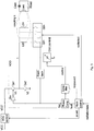
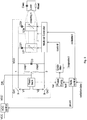
- FIG. 3 shows Figure 3 the block diagram of a series push-pull oscillator with a controlled capacitance in the resonance network.
- This oscillator is used here as a base unit in a wireless feed system, but it can be used as any oscillator.
- the switches Qv1 and Qv2 form a series push-pull stage (half bridge), which alternately switches its center point either to VCC 'or to a reference potential (ground).
- the switches Qv1 and Qv2 are always alternately open or closed.
- the switches Qv1 and Qv2 are of the same type (either two P-channel or two N-channel MOSFETs or either two PNP or two NPN IGBTs).
- the antiphase control signals V1 and V2 are guaranteed by the inverter (Inv).
- the switches Qv1 and Qv2 are complementary types (P / N channel MOSFETs or PNP / NPN bipolar transistors or IGBTs); Inv is not implemented there.
- the switch center point is connected to a series resonant circuit consisting of one or more inductances L01 ... L0n and one or more controlled capacitances Ctot with a reference potential (ground). At least one inductance L01 is actively present in the resonant circuit. If several inductances are used, any number of them are coupled to the resonant circuit via switches Q01 ... Q0n.
- a load unit comprises a load resistor (Rload), a tapping inductance (Lsec) and often, but not necessarily, a capacitor Csec, which tunes a load unit to the resonance frequency of the base unit.
- Rload load resistor
- Lsec tapping inductance
- Csec capacitor
- a parallel resonant circuit is also used in the load unit (not shown).
- the coordination in the load unit is based on series or Parallel resonance, but it is not critical because the attenuation of Rload increases the bandwidth significantly. All or any number of the inductances L01 ...
- L0n are implemented as open coils and couple one or more load units to the resonance circuit of the base unit. If several inductors L01 ... L0n are used, they are positioned on one surface or on several surfaces that are at an angle to one another. If the corresponding coupling switch Q01 ... Q0n is closed, the current through the corresponding inductance L01 ... L0n generates an induction vector. In this way, the induction field can be distributed as desired over an area or a limited space. In this way, the radiated induction field is advantageously concentrated on the positions of the load units. So only those inductances L01 ... L0n are coupled to the resonance network which transmit power to the load units.
- inductance L01 ... L0n coupled to the resonance network.
- inductance L01 which is permanently wired to the resonance network, is used in the power transmission.
- the arrangement can be viewed as an open transformer, the coupling k of which varies greatly with the geometric positioning and with the distance from L01 ... L0n to Lsec.
- a feedback closes a feedback loop from the resonance network to the switch input V1 or V2.
- At one pole of the impedance which is formed by L01 ... L0n, Ctot and the coupled part of Csec and Lsec, there is zero degrees between voltage and current in the resonance network.
- the switches and the feedback block together also have zero degrees in their transfer function.
- the phase condition is fulfilled so that a sustained oscillation can arise.
- the amplitude condition is also fulfilled because the resulting damping by Rload is smaller than the gain of the loop (Qv1, Qv2, resonance network and feedback).
- the feedback block picks up a partial flow from the resonance network and generates a square wave driver signal for V1 or V2. This driver signal is also tapped and sent to a Phase locked loop (PLL) forwarded as fist.
- PLL Phase locked loop
- a phase comparator Compares fist with a reference frequency (fsoll) and filters the resulting error signal in the loop filter. The filtered error signal thus controls the capacitance of the resonance network Ctot.
- VCO voltage-controlled oscillator
- phase comparator Phase Comp.
- the filtered error signal readjusts the capacitance Ctot until the oscillator frequency (fist) is again the same as the reference frequency (fsoll). This compensates for different inductance values L01 ... L0n, changes in the load unit, component value changes and changing coupling conditions.
- the residual error is always zero due to the integrating part of the PLL control loop.
- the phase error correction speed is determined by the response time of Ctot and the stability in the PLL.
- Ctot has a response time of half an oscillating circuit period. This means that the PLL loop can be dimensioned in such a way that it is closed again as quickly as possible if it disengages. This favors PLL-based synchronization systems over software control circuits for such applications because the hardware outlay is small and the locking time is minimal. This is due to the fact that the PLL phase comparator generates at least one error signal for each network period which influences the adjustment.
- a PLL lock-in time (step response to an fsoll change) of less than 100 oscillator frequency periods can be easily achieved with a 2nd order low-pass filter (loop filter), provided that no frequency advantage is used in the oscillator signal feedback.
- Software-based PLL control loops with the same properties can only be implemented with considerably greater effort because the loop is within one oscillator period has to do all PLL control loop calculations (phase error calculation and low-pass filtering).
- the operating voltage VCC ' is controlled by pcont in the VCC control block. This controls the oscillator or resonance network current / voltage amplitude and consequently the energy of the radiated induction field.
- Coilselect controls the switches Q01 ... Q0n and corresponds to a selection signal of the inductances L01 ... L0n, which are coupled to the resonance network. Coilselect controls the geometric induction field distribution.
- the Radicontrol block generates the required signals pcont, coilselect, fsoll and loopselect.
- the control signal radiationdata contains parameters which are required for the generation of pcont, coilselect, fsoll and loopselect.
- Radiationdata contains a first data group which is required for the generation of pcont. These are data that define pcont directly and / or data that define how pcont should change over time. Thus, based on a first value of the first data group, Radicontrol generates a control signal (pcont) for VCCcontrol, which generates pulses at VCC 'and accordingly results in a burst operation in the oscillator. Radicontrol also generates a control signal (pcont) for VCC control based on a further value of the first data group, whereby VCC 'and, accordingly, the emitted field energy can be continuously changed.
- Radiationdata contains a second data group that is required for generating coilselect. These are data that define coilselect directly and / or data that define how coilselect should change over time. Radiationdata contains a third data group which is required for generating fsoll. These are data that define fsoll directly and / or data that define how fsoll should change over time. Radicontrol generates loopselect based on the coilselect signal and if fset is more than one threshold value (e.g. 10%) it also changes based on fset. Loopselect modifies the PLL loop gain within the loop filter using e.g. E.g. modifying the charge pump current in the output of the phase comparator. Is z. E.g.
- Radicontrol can independently generate the 3 independent transmission parameters: radiated field energy, the area or space of the radiated field and the frequency of the radiated field.
- the radiated field energy can be controlled by pcont at any spectral position (fsoll) and at any spatial position.
- a different radiation image can be generated with a simple modification of radiationdata.
- So z. For example, country-specific reduced field radiation values can be generated at any spectral position in a simple manner.
- the third data group of radiationdata contains data which cause Radicontrol to generate no reference frequency (fsoll) at the corresponding spectral positions.
- Radicontrol changes the reference frequency (fsoll) continuously (sweep) and in a further embodiment stochastically in order to spectrally distribute the induction field.
- This is implemented taking into account frequencies fsoll that are not to be used.
- This advantageously reduces the maximum amount in the frequency spectrum and higher powers can be transmitted until the maximum limit value of the guidelines defined by the legislator is reached.
- Another advantage is that other users of the same frequency range are less disturbed and can therefore share the frequency range better.
- several users can negotiate the frequency range with one another, so that interference with one another is minimal.
- the big advantage of Frequency tracking circuits using a phase-locked loop (PLL) is the independence of the oscillator amplitude. In this, the oscillator always oscillates under its ideal conditions (phase and amplitude conditions). As a result, the radiated induction field remains constant when the frequency changes.
- PLL phase-locked loop
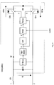
- FIG 4 shows a block diagram of a controlled large-signal capacity (Ctot (control)) according to Figure 3 .
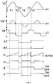
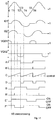
- Signal waveforms too Figure 4 are in Figure 5 and are used in the further description with its indices.
- the coupling to the oscillator takes place via the connections 1 and 2.
- the inductance L01 shown here as one of several inductances L01 ... L0n
- the capacitor CM is coupled to C0 via the coupling switches Q1a and Q1b.
- the diodes shown indicate that the coupling switches can only be controlled in one direction. In the opposite current direction, Q1a and Q1b remain bridged by the diodes.
- the term switch functionally defines the actively controllable part of Q1a and Q1b.
- the term coupling switch functionally defines the actively controllable part and the diode.
- the first extreme condition of the switch control occurs when the coupling switches Q1a and Q1b are always open. Then the resulting total capacitance is equal to C0 and is therefore minimal.
- the resonant circuit frequency is correspondingly at its maximum.
- the second extreme condition of the switch control occurs when the coupling switches Q1a and Q1b are always closed. Then the resulting total capacitance is the same as the parallel connection of C0 and CM and is therefore a maximum.
- the resonant circuit frequency is correspondingly minimal.
- Partial interval coupling means that C0 and CM are coupled to one another during part of the resulting resonant circuit period. In the following description, this is to be understood as a time or angle interval.
- the entire circuit represents a total capacity (Ctot), the value of which is controlled by Control.
- the resonant circuit frequency is the mean value of the entire resonant circuit period.
- the current oscillating circuit frequency changes within the oscillating circuit period between minimum and maximum or maximum and minimum frequency according to the states of the two coupling switches.
- the resulting capacitor voltage V0 is tapped in the V-Sense block and then fed to the Sign Detect block to determine the sign.
- the tapping of the capacitor voltage can also include only a partial voltage; it is only important that the sign of the output signal has a defined phase reference to the voltage V0 across the capacitor C0.
- the resulting waveform is shown in A.
- the following differentiator (Diff) derives A according to the time and outputs its amount, see curve B. This results in positive pulses at every zero crossing 0, T3 and T6 of the resonant circuit voltage V0.
- the pulse width modulator (PWM) generates a sawtooth C (in Figure 4 not shown because it is a signal within the PWM modulator). This sawtooth curve C is compared with the control variable control within the PWM block. If control is less than C, the PWM output D is high. If control is greater than C, the PWM output D is low.
- the modulator can be implemented in various ways based on the known pulse width modulation (PWM). It is only essential that the PWM signal D is triggered by B and its pulse length is controlled by control. This pulse length corresponds to a controlled delay that is controlled by control from the trigger moment (signal B).
- the following block Demux uses signal A to select a portion of the corresponding half-wave and feeds it to switches Q1a and Q1b. When A is high, the negated signal D controls switch Q1a through E. If A is low, the negated signal D controls switch Q1b via F. If D is not linked via A to the corresponding output E or F, E or F remains high. The switch Q1a or Q1b is closed (ON) when E or F is high. If E or F is low, Q1a and Q1b are open.
- PWM pulse width modulation
- the switches always remain closed for at least half a period and bypass their internal diode. This results in smaller on-state losses and prevents settling transients from occurring when the diodes are switched on.
- the stored energy in L0 forces a negative current flow in the internal diode of the coupling switch Q1a. This lasts from T2 to T3 and is replaced by the conductive (or inversely conductive) switch Q1a.
- the coupling switches Q1a and Q1b remain closed until the signal F goes low.
- a negative sinusoidal voltage half-wave develops in the sum voltage VQ1 during the time interval from T4 to T5. No current flows through CM during this interval. If the voltage VQ1 becomes zero (time T5), the stored energy in L0 forces a negative current flow in the internal diode of the coupling switch Q1b.
- FIG. 6 A parallel push-pull oscillator, which delivers more power compared to the half bridge with the same circuit complexity.
- a symmetrically tapped coil (Ltap1 and Ltap2) is alternately switched to a reference potential (ground) at both ends via a switch (Qv1 and Qv2).
- Ltap1 and Ltap2 At the two ends of Ltap1 and Ltap2, one or more controlled inductances (L0) and one or more additional inductances L01 ... L0n are coupled to Ltap1 and Ltap2. Alternatively, this is implemented using additional series capacities (not shown).
- the capacitance C0 forms a parallel resonant circuit with Ltap1, tap2, L0 and L01 ... L0n. If several inductances L01 ... L0n are used, any number of them can be coupled to the resonant circuit via switches Q01 ... Q0n. Additional series inductances and their switches can be implemented in any branch Q0n, L0n (not shown). These switches bridge the series inductances depending on the control. Such extended inductance arrangements can be necessary with high VCC ', higher transmittable powers and / or several load units.
- a load unit comprises a load resistor (Rload), a tapping inductance (Lsec) and often, but not necessarily, a capacitor Csec, which tunes a load unit to the resonance frequency of the base unit.
- a parallel resonant circuit is also used in the load unit (not shown).
- the tuning in the load unit takes place on series or parallel resonance, but it is not critical because the attenuation of Rload increases the bandwidth significantly.
- All or any number of the inductances Ltap1, Ltap2, L0, L01 ... L0n are implemented as open coils and couple one or more load units to the resonance circuit of the base unit. If several inductors Ltap1, Ltap2, L0, L01 ... L0n are used, are they positioned on one surface or on several surfaces that are at an angle to each other. If the corresponding coil coupling switch Q01 ... Q0n is closed, the current through the corresponding inductance L01 ... L0n generates an induction vector.
- the induction field can be distributed as desired over an area or a limited space.
- the radiated induction field is advantageously concentrated on the positions of the load units. So only those inductances L01 ... L0n are coupled to the resonance network which transmit power to the load units. If there is only one load unit, its coupling with the base unit can be improved by several inductances L01 ... L0n coupled to the resonance network.
- the arrangement can be viewed as an open transformer in the near field, the coupling k of which varies greatly with the geometric positioning and with the distance from Ltap1, Ltap2, L0, L01 ... L0n to Lsec.
- the feedback closes a feedback loop from the resonance network to the switch input of Qv1 and Qv2.
- the coil DR acts as a filter in the supply line and thus reduces the harmonic distortion of the push-pull stage (Qv1, Qv2).
- DR acts as a current source on the tapping point and thus allows full-wave rectification voltage, the mean value of which is equal to VCC ', to arise at the tapping point.
- the minimum value of the voltage at the tapping point corresponds to the voltage zero crossing of the voltage across C0.
- This voltage zero crossing or the minimum value of the voltage at the tapping point of the coils Ltap1, Ltap2 triggers a frequency divider within the feedback block.
- the inverted or the non-inverted output of the frequency divider controls Qv1 or Qv2. Is z.
- a sinusoidal voltage half-wave with half the voltage amplitude of the voltage across C0 is formed at the input of the feedback block. If this voltage reaches its minimum, the frequency divider is triggered and the driver signals from Qv1 and Qv2 change their states. Qv2 is closed and Qv1 is open. A sinusoidal voltage half-wave is formed again with half the voltage amplitude of the voltage across C0. You reach this tension The frequency divider is triggered at a minimum and the driver signals from Qv1 and Qv2 change their states again.
- phase comparator Phase Comp.
- the error signal from the Phase Comp. is then filtered in the loop filter block.
- the filtered error signal controls the inductance L0 of the resonance network. If the oscillator does not swing to fsoll, or if the reactance in the oscillator goes out of tune, an error signal results at the output of the phase comparator (Phase Comp.).
- the filtered error signal readjusts the inductance L0 until the oscillator frequency (fist) is again the same as the reference frequency (fsoll). This compensates for different inductance values L01 ...
- L0n changes in the load unit, component value changes and changing coupling conditions.
- the residual error is always zero due to the integrating part of the PLL control loop.
- the control speed is determined by the response time of L0 and the stability in the PLL.
- L0 has a response time of half an oscillating circuit period. This means that the PLL loop can be dimensioned in such a way that it is closed again as quickly as possible if it disengages.
- Figure 7 shows the block diagram of a controlled large-signal inductance (L0 (control)) according to Figure 6 .
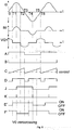
- Signal waveforms too Figure 7 are in Figure 8 and are used in the further description with its indices. It is coupled to the oscillator via connections 1 and 2.
- the resulting total inductance Ltap (from Ltap1 and Ltap2) is in Figure 7 shown. Together with the capacitance C0, it forms a parallel resonant circuit.
- the inductance LM is coupled to Ltap via the coupling switches Q1a and Q1b.
- the first An extreme condition of the switch control occurs when both coupling switches Q1a and Q1b are always open. Then the resulting total inductance is equal to Ltap and is therefore a maximum.
- the resonant circuit frequency is correspondingly minimal.
- the second extreme condition of the switch control occurs when both coupling switches Q1a and Q1b are always closed. Then the resulting total inductance is equal to the parallel connection of Ltap and LM and is therefore minimal.
- the resonant circuit frequency is correspondingly at its maximum. For partial interval coupling of LM with Ltap, any intermediate value of the two extreme values for the total inductance can be set via the control input.
- the entire circuit represents a total inductance (L0), the value of which is controlled by control.
- the resonant circuit frequency is the mean value of the entire resonant circuit period.
- the current oscillating circuit frequency changes within the oscillating circuit period between minimum and maximum or maximum and minimum frequency according to the states of the two coupling switches.
- the resulting coil current is tapped in the I-Sense block and then fed to the Sign Detect block to determine the sign.
- the tapping of the coil current can also only include a partial current of I0; it is only important that the sign of the output signal has a defined phase relation to the current I0 in the coil Ltap.
- the resulting waveform is shown in A.
- the following differentiator (Diff) derives A according to the time and outputs its amount, see curve B. This results in positive pulses at every zero crossing 0, T3 and T6 of the resonant circuit current I0.
- the pulse width modulator (PWM) generates a sawtooth C (in Figure 7 not shown because it is a signal within the PWM modulator). This sawtooth curve C is compared with the control variable control within the PWM block. If control is less than C, the PWM output D is high.
- the modulator can be implemented in various ways based on the known pulse width modulation (PWM). It is only essential that the PWM output signal D is triggered by B and by control in its pulse length is controlled. This pulse length corresponds to a controlled delay that is controlled by control from the trigger moment (signal B).
- the V-Sense block picks up the voltage via Ltap and the Sign Detect block detects the sign of this voltage, see signal J.
- the following differentiator (Diff) derives J after the time and outputs its amount, see curve K.
- the pulses of signal K coincide in time with the maxima or minima of the current I0.
- the signal K is combined with A and D in the demux in order to generate the drive signals E 'and F' of the switches Q1a and Q1b.
- the switch Q1a or Q1b is closed (ON) when E 'or F' is high. If E 'or F' is low, Q1a or Q1b is open.
- the signal D controls the closing of switch Q1a via E '(see time T1). If A is low, the signal D controls the closing of switch Q1b via F 'see (time T4). The transition from high (ON) to low (OFF) in E 'and F' is controlled by signal K with A, see times V0 zerocrossing in E 'and F'. The signal A selects which switch is controlled. If A is low, switch Q1a opens via E 'with K. If A is high, switch Q1b opens via F' with K. The switches always remain closed for at least half a period and bypass their internal diode. This results in lower transmission losses and prevents the occurrence of settling transients when the diodes are switched on.
- the coupling switch Q1b closes and a negative sinusoidal current half-wave develops in IM during the Time interval from T4 to T5. During this interval the total coupling switch voltage VQ1 is zero because both coupling switches are closed. If the current IM becomes zero again at time T5, the stored energy in C0 forces a negative voltage jump in the internal diode of Q1a, which results in an interruption of the current flow.
- the current flow interval of the internal diodes is limited to the interval from V0 zerocrossing to T2 of the positive current half-cycle in IM or T5 of the negative current half-cycle in IM.
- L0 control
- L0 can be divided into two or more parallel controlled inductors. Either one or two switches (Q1a and / or Q1b) are available for each partial inductance L0 (control). If only one switch is implemented per partial inductance L0 (control), then only one switch is implemented in the second partial inductance, namely in such a way that the total current according to the signal IM of Figure 8 results. In this way, the symmetry is advantageously maintained and the harmonic component in the oscillator and in the radiated induction field is kept to a minimum.
- FIG. 9 a parallel push-pull oscillator according to Figure 6 .
- the frequency control here includes not only a controlled inductance but at least one or more series circuits C01, L01 ... C0n, L0n, which are coupled to the parallel resonant circuit (Ltap1, Ltap2 and C0) via switches.
- the switches are integrated here in the Multicoil Controller block and they are used for frequency and induction field control.
- the corresponding input signals are the output of the loop filter (control) and coilselect from the Radicontrol block.
- the filtered error signal (control) controls one or more series circuits C01, L01 ...
- Phase comparator output Phase Comp.
- the filtered error signal regulates one or more series circuits C01, L01 ... C0n, L0n until the oscillator frequency (fist) is again the same as the reference frequency (fsoll). This compensates for different inductance values L01 ... L0n, changes in the load unit, component value changes and changing coupling conditions.
- the residual error is always zero due to the integrating part of the PLL control loop.
- the control speed is determined by the response time of the series circuits C01, L01 ...
- the series circuits C01, L01 ... C0n, L0n have a response time of half an oscillating circuit period. This means that the PLL loop can be dimensioned in such a way that it is closed again as quickly as possible if it disengages.
- the blocks VCC control and Radicontrol as well as their input and output signals behave identically to their names in Figure 3 . This means that the same operating modes are implemented.
- the coupling switch control of the resonance network according to Figure 9 is in Figure 10 shown.
- the corresponding signals are in Figure 11 and are used in the further description with their indices.
- the coupling to the oscillator is via the connections 1 and 2.
- the resulting total inductance Ltap (from Ltap1 and Ltap2) is in Figure 10 shown. Together with the capacitance C0, it forms a parallel resonant circuit.
- One or more series circuits C01, L01 ... C0n, L0n are connected via one or more coupling switches Q01 ... Q0n Ltap coupled.
- the first extreme condition of the switch control occurs when all coupling switches Q01 ... Q01n are always open. Then the resulting total inductance is equal to Ltap and is therefore a maximum.
- the resonant circuit frequency is correspondingly minimal.
- the second extreme condition of the switch control occurs when all coupling switches Q01 and Q01n are always closed. Then the resulting total inductance is minimal and equal to the parallel connection of Ltap and the resulting inductance of all series connections C01, L01 ... C0n, L0n.
- the resonant circuit frequency is correspondingly at its maximum.
- the series circuits C01, L01 ... C0n, L0n are dimensioned such that their series resonance for permanently closed switches Q01 ... Q01n is lower than the lowest network frequency or lowest oscillator frequency. In this case, the series circuits act as inductors and this allows the total inductance of the overall network to be controlled. For partial interval coupling of C01, L01 ...
- any intermediate value of the two extreme values for the total inductance can be set via the control input control.
- the resonant circuit frequency is the mean value of the entire resonant circuit period.
- the current oscillating circuit frequency changes within the oscillating circuit period according to the states of the coupling switches.
- the resulting coil current is tapped in the I-Sense block and then fed to the Sign Detect block to determine the sign.
- the tapping of the coil current can also only include a partial current of I0; it is only important that the sign of the output signal has a defined phase relation to the current I0 in the coil Ltap.
- the resulting waveform is shown in A.
- the following differentiator (Diff) derives A according to the time and outputs its amount, see curve B.
- the pulse width modulator (PWM) generates a sawtooth C (in Figure 10 not shown because it is a signal within the PWM modulator). This sawtooth curve C is compared with the control variable control within the PWM block. If control is less than C, that is PWM output D high. If control is greater than C, the PWM output D is low.
- the modulator can be implemented in various ways based on the known pulse width modulation (PWM). It is only essential that the PWM output signal D is triggered by B and its pulse length is controlled by control. This pulse length corresponds to a controlled delay that is controlled by control from the trigger moment (signal B).
- the V-Sense block picks up the voltage via Ltap and the Sign Detect block detects the sign of this voltage, see signal G.
- the following differentiator (Diff) derives G according to the time and outputs its amount, see curve H. This results positive pulses at each zero crossing of the resonant circuit voltage V0 (see V0 zerocrossing in Fig.11 ).
- the pulses of signal H coincide in time with the maxima or minima of the current I0.
- the signal H is linked with A and D in the demux in order to generate the driver signals E “and F” for the switches Q01 ... Q0n.
- the driver signals E “and F” are coupled to the corresponding coupling switches via the AND gates A01 ... A0n. E "is identical to 01, 03 ...
- 0n-1 and F is identical to 02, 04 ... 0n, if coilselect enables all ANDs A01 ... A0n on E “and F".
- the corresponding selection signals coil 01 select ... coil 0n select are coupled to the corresponding inputs of the ANDs by means of signal A. In this way, coil 01 select ... coil 0n select can change at any time. There is always a stable driver signal 01 ... 0n for every network period.
- the switches Q01 ... Q0n are closed (ON) when E “or F” is high. If E “or F” is low, Q01 ... Q0n are open. If A is high, the signal D via E “controls the closing of switch Q01 (see time T1).
- the signal D via F controls the closure of switch Q02 see (time T4).
- the transition from high (ON) to low (OFF) in E “and F” is controlled by signal H with A, see times V0 zerocrossing in E “and F”.
- the signal A selects which switch is controlled. If A is low, switch Q01 opens via E “with H. If A is high, switch Q02 opens via F” with H.
- the switches always remain closed for at least half a period and at least partially bypass their internal diodes. That causes smaller forward losses and prevents the occurrence of settling transients when the diodes are switched on. The diodes can still carry some residual current.
- the process leads to a reduction in losses, especially if the on-resistance of the switches (Rdson) is sufficiently small.
- E is high, the coupling switch Q01 closes and a current wave develops in I01.
- This current wave defines a coupling period which is twice as long as the interval from T1 to T3.
- the coupling switch voltage VQ01 is zero.
- T3 The entire energy of the series circuit C01, L01 is stored in C01.
- the current I01 passes through the zero point at time T3 and then discharges the capacitance C01 with a negative current I01 in the interval from T3 to T5.
- the current I01 becomes zero again at time T5 , the flow of current I01 to E "stops again, the series circuit C01, L01 couples to the rest of the resonance network. If F "is high, the coupling switch Q02 closes and a current wave develops in I02. This current wave defines a coupling period which is twice as long as the interval from T4 to T6. During this entire coupling period, the coupling switch voltage VQ02 is equal to zero. At time T6 the entire energy of the series circuit C02, L02 is stored in C02. Furthermore, the current I01 passes through the zero point at time T6 and then discharges the capacitance C02 with a positive current I02 in the following coupling half cycle.
- This coupling half cycle is identical to the interval from 0 to T2 If the current I02 is zero again at time T2, the current flow I02 to F ′′ stops again, which couples the series circuit C02, L02 to the rest of the resonance network.
- the resonance frequency of the overall network changes depending on the coupling of the series circuits with the overall network.
- the total network period is determined by C0, Ltap, C02 and L02.
- the total network period is determined by C0, Ltap, C01, L01, C02 and L02.
- the total network period is determined by C0, Ltap, C01 and L01.
- an inductance (L01... L0n) can be controlled with a symmetrical current wave.
- There are particularly few harmonics when a pair of series connections in anti-parallel connection see C01, L01, Q01 and C02, L02, Q02) are coupled together to the overall network.
- the radiation fields in the two inductances L01 and L02 compensate each other.
- a switch e.g. Q01
- a series connection e.g. C01, L01
- FIG 12 shows a detailed circuit of a parallel push-pull large-signal VCO according to the current invention.
- the oscillator essentially corresponds to that of the Figures 6 and 9 .
- Ltap1, Ltap2 are the radiation coils of the induction vector (or at least part of them).
- SMPS switched mode power supply
- the resonance circuit is connected to connections 1 and 2. In the simplest case, this is a controlled capacity. In a further exemplary embodiment, these are controlled capacitances / inductances or controlled series circuits of the two.
- RV9 and CV6 form a low-pass filter that dampens transients.
- QV7, DV3 and RV7 form the voltage minimum detector whose reference voltage is applied to the emitter of QV8 filtered with CV5. The reference voltage is determined by the voltage divider RV6 and RV8.
- QV9 is only responsible for the oscillation and is therefore always conductive in normal operation via RV5.
- RV10 and CV7 make the reference voltage proportional to the mean value of the input voltage. This means that QV7 opens regardless of the output voltage from the SMPS at the minimum voltage via CV6.
- the resulting pulses at the collector QV7 trigger the flip-flop FFV. This causes its outputs Q and IQ to flip.
- QV6 are controlled with opposite signals via CV1 and CV2, which changes the switch states of Qv1 and Qv2.
- the capacitors CV1, CV2, RV3 and RV4 ensure that both switches Qv1 and Qv2 always remain open if there is no pulse at the input of FFV.
- Both inputs of the drivers are always grounded via RV3 and RV4.
- DV1 and DV2 clamp the square voltages to ground in normal operation. This results in driver voltage levels of approx. 0 ... 12V.
- the circuit is started up via the time constant RV5, CV4.
- the reference voltage across CV5 is initially equal to the voltage across CV7 and QV7 is therefore open. If QV9 becomes conductive, the reference voltage drops via CV5 and QV7 switches on.
- the trigger signal from FFV is coupled to the phase comparator (Phase Frequency Detector PFD) as fist.
- the comparison frequency (fsoll) is determined via a controlled frequency divider (RefDiv) from a reference frequency (fref) z. E.g. 32MHz derived.
- the PFD corresponds to that of the known circuit from the CMOS component 4046.
- the PFD output signals are used here independently via the resistors RP1 ... RP4 via a current mirror QV8, QV10 or QV7, QV9 to the loop filter CP1, CP2 and RP7.
- the QV11 transconductance amplifier generates the control current for the controlled admittances via the loop filter in proportion to the control voltage.
- the PLL loop gain is switched over via the analog switch SW via RP2 and RP3. This changes the charge pump current from QV9 and QV10, which flows into the loop filter.
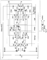
- FIG. 13 shows a detailed circuit of a controlled capacitance according to the block diagram of FIG Figure 4 .
- the dashed lines encompass parts of the block diagram. It is coupled to the oscillator via connections 1 and 2.
- CM is designed as a series circuit of 2 capacitors CM1 and CM2, which is coupled to C0 via Q1a and Q1b.
- the switch control is operated on a supply voltage of +12 '.
- An optocoupler (OPTO) transmits the control information (control) in an electrically isolated manner, as the switch control is galvanically isolated by +12 'from the rest of the network.
- OPTO optocoupler
- the capacitors C1 and C2 pick up the positive voltage half-cycle from V0 and lead it via R1 to the base of transistor Q10.
- Q10 acts as a kind of voltage zero point detector of the positive half-wave.
- D1 and D3 accelerate the shutdown as soon as the voltage across C2 falls below the threshold voltage of Q10.
- the capacitive voltage divider C1, C2 prevents a DC voltage coupling with V0.
- a phase advance can be achieved via R1, C1 and C2.
- these components are dimensioned so that the phase advance is at least as great as the total signal delay of the control circuit. This means that the entire modulation range can be used.
- the components Q9, D2, D4, R3, R4, C3 and C4 work identically to the components around Q10, only they are responsible for the negative half-wave of V0.
- the two D flip-flops FF1, FF2 and the NAND gate N1 detect the two positive edges of the output signals of the voltage zero point detectors Q9 and Q10.
- voltage pulses arise at the output of N1 at each zero crossing of V0 (signal curve B), which briefly fully control transistor Q2.
- This symmetrical implementation guarantees identical behavior with regard to the two voltage half-waves of V0.
- Q2 is only coupled to V0 during the trigger moment of the short voltage pulses.
- Q7, Q8, R6 and R5 reflect a control current, defined by the control variable control, which flows into the capacitor C5.
- the result is a sawtooth voltage across C5 (curve C), which reaches its lowest value in time with the control pulses from Q2.
- This sawtooth voltage triggers FF5 via the CK input as soon as its switching threshold is reached. This point in time can be controlled via the control input, because the slope of the sawtooth voltage can be changed by the collector current in Q8 and consequently with control.
- FF5, FF6, N3 and N4 form the first part of the demux.
- FF5 is configured via the pulses at the Set (S) or Reset (R) input so that the sawtooth always controls the corresponding switch that is responsible for the corresponding half-wave. This corresponds to the switching signal selection using signal curve A. If V0 appears with the positive half-wave, D2 is conductive. Q9's collector is high and triggers FF2 via CK. The briefly set output Q of FF2 sets the output Q of FF5 via its Set (S) input. The low at the output IQ of FF5 forces a high at the output of N4, which closes Q1a via the drivers Q3, Q4. This is the initial condition for the controlled decoupling of CM1 and CM2 during the positive half-cycle of V0.
- S Set
- R Reset
- FF5 tips over: Q is low and IQ is high.
- the IQ of FF6 is also high, as a result of which the output of N4 switches to low, consequently the coupling switch Q1a opens via the drivers Q3, Q4.
- FF5 is reset via the R input of FF1 as soon as D1 is conductive and FF1 is triggered via the clock CK.
- N3 or N4 which was previously low at the output, goes to high.
- both switches Q1a and Q1b always remain closed from this point in time until the PWM modulator opens one of the two switches again.
- the flip-flop FF6 synchronizes itself at the latest after one resonant circuit period after switching on the entire circuit. Then at least one of the coupling switches Q1a or Q1b has always opened once and generated a clock pulse for FF6.
- Figure 14 shows a detailed circuit of a controlled series circuit of inductance and capacitance according to the block diagram of FIG Figure 10 .
- the dashed lines encompass parts of the block diagram. It is coupled to the oscillator via connections 1 and 2.
- the curve shapes of the Figure 11 referenced with their indices. L01, C01, L02, C02, L03, C03 and L04, C04 are coupled to C0 via Q01 ... Q04.
- the required control signals 01 ... 04 of the coupling switches Q01 ... Q04 are electrically isolated from the outputs of the NAND gates N3 ... N6 and coupled to Q01 ... Q04 via the transformers T1 ... T4.
- optocouplers with the following driver can be used (not shown).
- the NANDs N3 ... N6 form the multiplexer which selects the switch control outputs of the flip-flops FF5 and FF6 depending on the selection signals coil 01 select and coil 02 select latched by FF7 and FF8. If coil 01 select or coil 02 select is high, the corresponding NANDs (N3, N4 or N5, N6) are transparent and loop the output signals from FF5 and FF6 to the corresponding pair of coupling switches (Q01, Q02 or Q03, Q04). In a further variant, all 4 inputs of the NANDs N3 ... N6 can be selected via 4 control lines coil 01 select ... coil 04 select. The switch control is operated at a voltage of +12 with any reference potential.
- the inductance L1 picks up the positive current half-wave from I0 and leads it via R1 and C2 to the base of transistor Q10.
- Q10 acts as a quasi current zero point detector of the positive half-wave.
- D1 and D3 accelerate the shutdown as soon as the current through C2 changes its sign.
- C2 also prevents DC coupling with I0.
- the current sense network is designed in such a way that there is a phase advance. This means that the entire modulation range can be used.
- the components Q9, D2, D4, R3, C4 and L2 work identically to the components around Q10, only they are responsible for the negative current half-cycle of I0.
- the two D flip-flops FF1, FF2 and the NAND gate N1 detect the two positive edges of the output signals of the current zero point detectors Q9 and Q10.
- a flip-flop (FF1 or FF2) at output Q switches to high as soon as it is triggered at clock CK. This state is immediately reset via the corresponding reset input after the runtime of N1.
- voltage pulses arise at the output of N1 at every zero crossing of I0 (signal curve B), which briefly fully control transistor Q2.
- This symmetrical implementation guarantees identical behavior with regard to the two current half-waves of I0.
- Q2 is only coupled to I0 during the trigger moment of the short voltage pulses.
- Q7, Q8, R6 and R5 reflect a control current that flows into capacitor C5 and is controlled by the loop filter via connection 3 (control).
- a sawtooth voltage arises across C5 (curve C), which reaches its lowest value with the modulation pulses from Q2.
- This sawtooth voltage triggers FF5 via the CK input as soon as its switching threshold is reached. This point in time can be controlled via the control input, because the slope of the sawtooth voltage is determined by the collector current in Q8 and consequently with control can change.
- FF5, FF6, N3 and N4 form the demux.
- FF5 is configured via the pulses at the Set (S) or Reset (R) input so that the sawtooth always controls the corresponding switch that is responsible for the corresponding half-wave.
- L04, C04 is only determined by the integrated diodes in Q01 ... Q04. A phase lead in the V-Sense block is no longer absolutely necessary. The important boundary condition that switches Q01 ... Q04 open at the latest when the internal diodes open remains fulfilled.
- the flip-flops N7 and N8 take over the inverted state of coil 01 select or coil 02 select with each PWM trigger pulse (output of N1). This means that the number of series oscillating circuits L01, C01 ... L04, C04 can be changed as required with a time resolution of half a network period.
- the advantage of differentiation is the robustness against transients, which only interfere with the function when the sign of the total voltage (V0) changes. This makes the "switch-off command" of switches Q01 ... Q04 insensitive to transients in the resonance circuit.
- the flip-flop FF6 synchronizes itself, at the latest one resonant circuit period after switching on the entire circuit.
- the capacitors C01... C04 are not equipped and are replaced by bridges in Figure 14 .
- the VCO corresponds to the execution according to Figures 7 and 8th with multiple inductances.
- the controller in Figure 12 generates pcont, coilselect (containing the signals coil 01 select and coil 02 select) and fsoll according to the input data contained in radiationdata. Loopselect is generated from the coilselect data.
- loopselect is generated based on the data coilselect and RefDivvalue.
- RefDivvalue divides fref and thus generates fsoll.
- RefDivvalue is unchanged over time and generates a discrete VCO spectral line (measured according to EN300330). This spectral line is controlled by the controller via Refdivvalue and fsoll according to data within radicontrol.
- Fsoll is constant therein during an energy transfer interval.
- An energy transmission interval is a time-limited section which is characterized by an induction vector (measured current in a radiation coil) that is greater than 1 ... 10% of its maximum possible value.
- RefDivvalue changes over time and distributes an induction vector (measured current in a radiation coil) to at least two spectral positions.
- RefDivvalue or fsoll changes so quickly that an induction vector (measured current in a radiation coil) is distributed over several spectral lines or a spectral range (measured according to EN300330).
- the controller generates RefDivvalue values which continuously output random values from a range of values limited by a minimum and a maximum. These values are generated according to a pseudo random sequence (PRS) and describe a sine (x) / x in at least one sub-spectrum of the induction vector spectrum (measured current in a radiation coil).
- PRS pseudo random sequence
- the controller RefDivvalue generates values which output a continuous sweep sequence as values from a value range limited by a minimum and a maximum value.
- a sweep sequence is characterized by the fact that the output values change periodically from a minimum value to the maximum value and then from the maximum value to the minimum value, etc.
- Figure 15a shows a period one such a sweep sequence (RefDivvalue (t)), whereby the dwell time (time interval which outputs the same RefDivvalue) on the time axis (t) changes dynamically depending on RefDivvalue. For example, a dwell time of one time unit applies to min and max and, on the other hand, to an average of min and max a dwell time that is five times longer.
- the increment of the values RefDivvalue is not constant.
- Figure 15a approximate a cubic function in RefDivvalue (t). Such a function generates a uniform spectrum and is characterized by an approximately equal maximum value IPI max (f) (see Figure 15b ).
- RefDivvalue not all possible Refdivvalue values are output in RefDivvalue (t). So becomes like in Figure 16a shown, the value "blacklisted RefDivvalue" is not used in the sweep sequence. This has the consequence that fsoll does not generate a frequency at the point fref divided by "blacklisted RefDivvalue”. This also results in no spectral component at the corresponding point in the VCO frequency. In this way, any incisions can be made in IPI max (f) (see Figure 16b ). It is clear that this method can be applied to any RefDivvalue (t) sequence, regardless of whether it is a sweep sequence or a PRS.
- the controller in Figure 12 In one embodiment, generates pcont- and fsoll values that result in any spectral distribution including incisions (e.g. according to EN300330, REC7003 and ITU-RSM2123).
- Pcont is either determined by the power control between the base and load unit or, if necessary, limited by the maximum values of the standards mentioned.
- Corresponding RefDivvalues (min, max and one or more blacklist RefDivvalue) are advantageously stored as parameters in a memory.
- a memory also stores parameters for pcont and parameters that determine the dwell time of RefDivvalue (t).
- the controller can be designed as a discrete digital network, integrated logic circuit (PLD, FPGA) or as a microcontroller.
- RAM / ROM memories are integrated in integrated circuits (PLD, FPGAs and microcontrollers with integrated memory).
- data input / output interfaces such as pcont, radiationdata, coilselect and Refdivvalue
- the controller implementation can also be implemented in an extremely compact and cost-effective manner, depending on the requirements or requirements.
- All LC-based AC generators and all LC oscillator options in connection with controlled capacitances and / or controlled inductances and / or controlled combination circuits of both can be set up.
- the simplest embodiment of the current invention is an alternating voltage generator with a tunable resonance network.
- the switches Qv1 and Qv2 are controlled with any external signal.
- the independent control signals (V1 and V2) (decoupled from the oscillator) result in greater freedom in the generator design. This can be of interest if exact resonance tuning can be neglected or the bandwidth in the resonance circuit is very high.
- Another embodiment of the current invention is the operation of several VCOs according to the current invention, which work together on induction coils. Since the currents and voltages in the resonance circuit are all defined in terms of time (phase position) in the VCOs Induction field superposition can be implemented particularly easily by means of the current invention.
Landscapes
- Engineering & Computer Science (AREA)
- Power Engineering (AREA)
- Computer Networks & Wireless Communication (AREA)
- Signal Processing (AREA)
- Inductance-Capacitance Distribution Constants And Capacitance-Resistance Oscillators (AREA)
Description
- Die aktuelle Erfindung bezieht sich auf die Generierung von elektromagnetischen Wellen mittels Resonanznetzwerk und insbesondere auf Leistungsübertragung im Nahfeld für RFID und drahtlose Speisungen. Des Weiteren bezieht sich die aktuelle Erfindung auf die Steuerung der Resonanzfrequenz eines Oszillators mittels geschaltenem Resonanznetzwerks.
- Drahtlose Energieversorgung von Geräten kann mittels induktiver- und / oder kapazitiver Nahfeldkopplung realisiert werden. Dies wird in vielen RFID Systemen und drahtlosen Batterieladegeräten eingesetzt.
- Eine Quelleneinheit, im Folgenden als Basiseinheit bezeichnet, generiert ein elektromagnetisches Wechselfeld dessen Strahlungseinheit meisst als Resonanzkreis ausgebildet ist. Durch den Resonanzkreis lässt sich ein Wechselfeld mit wenig Aufwand effizient erzeugen, weil die Treiberschaltungen praktisch keine Schaltverluste generieren (Zero Voltage ZVS- oder Zero Current Switching ZCS). Die Filterwirkung des Resonanzkreises beeinflusst die spektrale Leistungsdichte und unterdrückt Oberwellen.
- Ein Generator in der Basisstation treibt einen Resonanzkreis mit einem Signal, dessen Frequenz und Amplitude variert werden kann, um die zu übertragende Leistung zu steuern. Das mit Energie zu versorgende Gerät, im Folgenden als Lasteinheit bezeichnet, wird im Abstand eines Bruchteils der Wellenlänge des elektromagnetischen Wechselfeldes so plaziert, dass zwischen Basis- und Lasteinheit möglichst gute Kopplung besteht. Dazu wird auf gleiche Polarisation, minimale Distanz und auf grösste Kopplungsfläche optimiert. Oft werden auch zusätzliche weichmagnetische Materialien verwendet um die Kopplung weiter zu erhöhen und / oder den Feldverlauf zu lenken.
- Es ist bekannt, dass bei der Verwendung eines Resonanzkreises in der Lasteinheit die übertragbare Leistung bei gegebener Kopplung erhöht werden kann. Optimalerweise sollte der Lastresonanzkreis genau auf die Frequenz des magnetischen Wechselfeldes abgestimmt sein, wobei man aber einen Kompromiss zwischen erzielbarer Bandreite und Kopplungsgewinn abwägt.
- In "System description Wireless Power Transfer" ist ein Schwingkreis gezeigt, der von einem Generator getrieben wird. Hier wird über ein zuschaltbares Netzwerk eine Mehrzahl von Teilinduktivitäten an den Resonanzkreis zugeschaltet um die abgestrahlte Feldenergie auf die Fläche zu konzentrieren, wo Lasteinheiten positioniert sind. Weiter wird mit einem vorgeschalteten Spannungs- oder Stromregler die Speisung gesteuert.
- Der generelle Nachteil von drahtlosen Speisungsprinzipien, welche Resonanzkreise in der Basis und/ oder in der Lasteinheit verwenden, ist die Resonanzfrequenzverstimmung. Dies ist aufgrund von Komponententoleranzen, Komponentenalterung, Kopplung und Lastentnahme gegeben. Diese Lastverstimmung ist insofern unerwünscht, weil die Impedanz des Resonanzkreises frequenzselektiv wirkt und eine vorgegebene Betriebsfrequenz nicht mehr mit der Resonanzfrequenz übereinstimmt. Folglich sinkt der Gesamtwirkungsgrad der Treiberschaltung und somit der Leistungsübertragung von Basis- zu Lasteinheit. Zusätzlich erhöhen sich die Verzerrungen, weil die Treiberschaltungen mehr Oberwellen erzeugen.
- Die bekannte Netzwerkmessmethode misst zwar in einem Intervall die Resonanzfrequenz des Netzwerks und betreibt es anschliessend bei dieser Frequenz, hat aber keine Möglichkeit die Netzwerkfrequenz aktiv zu steuern. Dies wäre jedoch sehr wünschenswert, da in Richtlinien wie EN300330, REC7003 und ITU-RSM2123 Frequenzbereiche (z. Bsp. 119...135kHz) und deren maximale Amplitudenwerte bestimmt sind. Weiter existieren länderspezifische schmale Frequenzbereiche innerhalb eines Frequenzbandes die viel kleinere Grenzwerte verlangen.
- Es ist daher wichtig, neben der Leistung auch die spektrale Position der abgestrahlten Leistung zu steuern.
-
US6586895 zeigt wie man eine Induktivität oder ein Netzwerk höheren Grades mittels variablen Kopplungsintervalls während einer Teilperiode in beiden Halbwellen einer Schwingkreisperiode elektronisch steuert.Figur 1 zeigt die wesentliche Schaltung, darin bilden der Kondensator CS und die Induktivität LH einen Serienschwingkreis. Kondensator CM und die Induktivität LM werden über die gesteuerten Transistoren Q1a und Q1b und deren integrierten Dioden in zwei Teilintervallen der Schwingkreisperiode an CS gekoppelt. Die Kopplungssteuerung funktioniert in beiden Halbperioden des Schwingkreises, da der Strom in CM und LM in beiden Richtungen von der Ansteuerung der Transistoren Q1a respektive Q1b abhängig ist. Der Kondensator CR ist nicht relevant, da er über den Transistor QH und die Diode DH kurzgeschlossen bleibt; oder die Transistoren Q1a und Q1b ganz offen oder ganz geschlossen bleiben, wenn QH offen ist. - In "Stabilisation the Operating Frequency of a Resonant Converter for Wireless Power transfer to Implantable Biomedical Sensors" wird ein gesteuertes Resonanznetzwerk in einem Generator vorgeschlagen, dessen Lastresonanzkreis mittels variabler Kopplungsteuerung gesteuert werden kann (siehe
Figur 2a ). Dabei wird in einem LC- Schwingkreis ein zweiter Kondensator für Teilintervalle einer Schwingkreisperiode zum LC Schwingkreis gekoppelt (sieheFigur 2b ). Die Schaltersteuerung vergleicht die Resonanzspannung mit einer Referenzspannung die als Steuergrösse wirkt und generiert vom Vergleicherausgangssignal das Schaltsignal für die Kopplungsschalter (sieheFigur 2c ). Diese Steuerung arbeitet sehr unzuverlässig, da jede Änderung der Schwingkreisamplitude sofort die Frequenz des Schwingkreises mitbeinflusst. Amplitudenschwankungen der Resonatorspannung treten bei jeder angekoppelter Lasteinheit (bzw. deren Laständerung) auf. Zudem hat eine Amplitudensteuerung, die zur Leistungsregelung oft eingesetzt wird immer eine Frequenzverstimmung zur Folge. Die Amplitudensteuerung des Schwingkreises und dessen Frequenzsteuerung arbeiten nicht unabhängig voneinander. - Das Erzeugen von Steuersignalen, welche unabhängig sind von der zu steuernden Grösse ist sehr schwierig. Das Hauptproblem besteht darin, dass die ändernde Ausgangsgrösse sogleich die Eingangsgrösse ändert und somit das System instabil macht.
- Eine weitere wichtige Anforderung an einer Basisstation, deren Frequenz gesteuert werden kann, ist die Amplitudentreue. Wird die Frequenz geändert, sollte sich die Amplitude nicht ändern. Dies ist vor allem während dem plötzlichen Umschalten (Frequenzsprüngen) schwierig, da sich die Impedanz des Resonanzkreises je nach Frequenzsprung stark ändern kann.
- Wird ein Schwingkreis gebildet dessen Teilkomponenten mittels gesteuerter Teilintervallkopplung geändert werden können, ist es daher sehr wichtig, dass das Kopplungsintervall unabhängig von der Schwingkreisperiode und Schwingkreisamplituden gesteuert werden kann. Dies bedeutet die Schwingkreisfrequenz ist nur eine Funktion der Steuergrösse. Diese Unabhängigkeitsbedingung garantiert einen stabilen Betrieb unabhängig zur Güte im Resonanznetzwerk. Frequenz- oder Phasenregelschlaufen sollten möglichst kurze Fangzeiten aufweisen. Dadurch werden Frequenz- oder Phasenänderungen in Netzwerk sofort ausgeregelt. Zudem ist eine schnelle Regelschlaufe wichtig, um bei einem Sweepbetrieb einen Betriebsfrequenzbereich mit grosser zeitlicher Auflösung (kurze Verweilzeit) zu bewirtschaften.
- Die nachfolgende Erfindung beschreibt ein Verfahren und deren Detailimplementationen um die Frequenz bzw. Phase eines Generators über ein frequenzgesteuertes Grossignalnetzwerk zu steuern. Das beschriebene Verfahren erfüllt alle erwähnten Anforderungen und zeichnet sich mit kurzer Fangzeit, Güte unabhängigem stabilen Betrieb und hohem Wirkungsgrad aus.
-
-
Figur 1 zeigt eine Schaltung zur Steuerung der Frequenz in einem Grosssignalresonanznetzwerk nach einem ersten Stand der Technik. -
Figuren 2a...2c zeigen Schaltungen zur Steuerung der Frequenz in einem Grosssignalgenerator nach einem zweiten Stand der Technik. -
Figur 3 zeigt das Blockschaltbild eines Grosssignal VCOs gemäss einem ersten Ausführungsbeispiel der aktuellen Erfindung. -
Figur 4 zeigt ein Blockschaltbild einer gesteuerten Grosssignal Kapazität gemässFigur 3 . -
Figur 5 zeigt Signale zuFigur 4 . -
Figur 6 zeigt das Blockschaltbild eines Grosssignal VCOs gemäss einem zweiten Ausführungsbeispiel der aktuellen Erfindung. -
Figur 7 zeigt ein Blockschaltbild einer gesteuerten Grosssignal Induktivität gemässFigur 6 . -
Figur 8 zeigt Signale zuFigur 7 . -
Figur 9 zeigt das Blockschaltbild eines Grosssignal VCOs gemäss einem dritten Ausführungsbeispiel der aktuellen Erfindung. -
Figur 10 zeigt ein verfeinertes Blockschaltbildes zuFigur 9 . -
Figur 11 zeigt Signale zuFigur 10 . -
Figur 12 zeigt eine Detailschaltung eines Ausführungsbeispiels der aktuellen Erfindung. -
Figur 13 zeigt eine Detailschaltung eines Ausführungsbeispiels der aktuellen Erfindung. -
Figur 14 zeigt eine Detailschaltung eines Ausführungsbeispiels der aktuellen Erfindung. -
Figur 15 zeigt ein Frequenzmanagement der aktuellen Erfindung. -
Figur 16 zeigt ein erweitertes Frequenzmanagement der aktuellen Erfindung. - Gemäss einem ersten Ausführungsbeispiel zeigt
Figur 3 das Blockschaltbild eines Serie- Gegentakt Oszillators mit einer gesteuerten Kapazität im Resonanznetzwerk. Dieser Oszillator wird hier als Basiseinheit in einem drahtlosen Speisungssystem verwendet, er kann aber als beliebiger Oszillator eingesetzt werden. Die Schalter Qv1 und Qv2 bilden eine Seriegegentaktstufe (Halbbrücke), welche ihren Mittelpunkt abwechselnd entweder auf VCC' oder an ein Referenzpotenzial (Masse) schaltet. Die Schalter Qv1 und Qv2 sind immer abwechselnd offen oder geschlossen. In einem Ausführungsbeispiel handelt es sich bei den Schaltern Qv1 und Qv2 um gleiche Typen (entweder zwei P- Kanal oder zwei N- Kanal MOSFETs bzw. entweder zwei PNP oder zwei NPN IGBTs). Die gegenphasigen Ansteuersignale V1 und V2 werden durch den Inverter (Inv) garantiert. In einem weiteren Ausführungsbeispiel handelt es sich bei den Schaltern Qv1 und Qv2 um komplementärtypen (P/N Kanal MOSFETs bzw. PNP/NPN bipolar Transistoren oder IGBTs), dort ist Inv nicht implementiert. Der Schaltermittelpunkt ist mit einem Serieschwingkreis bestehend aus einer oder mehreren Induktivitäten L01... L0n und einer oder mehreren gesteuerten Kapazitäten Ctot mit einem Referenzpotential (Masse) verbunden. Mindestens eine Induktivität L01 ist aktiv im Schwingkreis vorhanden. Falls mehrere Induktivitäten verwendet sind, ist eine beliebige Anzahl davon über Schalter Q01... Q0n an den Schwingkreis gekoppelt. Dabei können in einem beliebigen Zweig Q0n, L0n zusätzliche Serieinduktivitäten und deren Schalter implementiert sein (nicht gezeigt). Diese Schalter überbrücken je nach Ansteuerung die Serieinduktivitäten. Solche erweiterte Induktivitätsanordnungen sind bei hohen VCC', höheren übertragbaren Leistungen und / oder mehreren Lasteinheiten erforderlich. Eine Lasteinheit umfasst einen Lastwiderstand (Rload), eine Abgreifinduktivität (Lsec) und oft, aber nicht zwingend einen Kondensator Csec, der eine Lasteinheit auf die Resonanzfrequenz der Basiseinheit abstimmt. Alternativ wird auch ein Parallelschwingkreis in der Lasteinheit verwendet (nicht gezeigt). Die Abstimmung in der Lasteinheit erfolgt auf Serie- bzw. Parallelresonanz, sie ist aber nicht kritisch, weil die Dämpfung von Rload die Bandbreite wesentlich erhöht. Alle oder eine beliebige Anzahl der Induktivitäten L01... L0n sind als offene Spulen implementiert und koppeln eine oder mehrere Lasteinheiten an den Resonanzkreis der Basiseinheit. Sind mehrere Induktivitäten L01... L0n verwendet, sind sie auf einer Fläche oder auf mehreren Flächen, welche in einem Winkel zueinander stehen positioniert. Ist der entsprechende Kopplungsschalter Q01... Q0n geschlossen, generiert der Strom durch die entsprechende Induktivität L01... L0n einen Induktionsvektor. So kann das Induktionsfeld auf einer Fläche bzw. einem begrenzten Raum beliebig verteilt werden. Vorteilhafterweise wird das abgestrahlte Induktionsfeld auf diese Weise auf die Positionen der Lasteinheiten konzentriert. Es werden also nur diejenigen Induktivitäten L01... L0n an das Resonanznetzwerk gekoppelt, welche Leistung an die Lasteinheiten übertragen. Falls nur eine Lasteinheit vorhanden ist, kann derren Kopplung mit der Basiseinheit durch mehrere an das Resonanznetzwerk gekoppelte Induktivitäten L01... L0n verbessert werden. Alternativ wird in einem Ausführungsbeispiel nur eine Induktivität L01, welche permanet mit dem Resonanznetzwerk verdrahtet ist, in der Leistungsübertragung verwendet. Die Anordnung kann im Nahfeld als offener Transformator betrachtet werden, dessen Kopplung (coupling k) stark mit der geometrischen Positionierung und mit dem Abstand von L01... L0n zu Lsec variert. Ein Feedback schliesst eine Rückkopplungsschlaufe vom Resonanznetzwerk zum Schaltereingang V1 bzw. V2. Bei einem Pol der Impedanz, welcher durch L01... L0n, Ctot und dem gekoppelten Anteil von Csec und Lsec gebildet wird, ergibt sich null Grad zwischen Spannung und Strom im Resonanznetzwerk. Die Schalter und der Feedback Block weisen zusammen in ihrer Übertragungsfunktion auch null Grad auf. Somit ist die Phasenbedingung erfüllt damit eine anhaltende Schwingung entstehen kann. Die Amplitudenbedingung ist ebenfalls erfüllt, weil die resultierende Dämpfung durch Rload kleiner ist als die Vestärkung der Schlaufe (Qv1, Qv2, Resonanznetzwerk und Feedback). Der Block Feedback greift ein Teilstrom vom Resonanznetzwerk ab und generiert ein Rechteck Treibersignal für V1 bzw. V2. Dieses Treibersignal wird zusätzlich abgegriffen und an eine Phaseregelschlaufe (Phase Locked Loop PLL) als fist weitergeleitet. Darin vergleicht ein Phasenvergleicher (Phase Comp.) fist mit einer Referenzfrequenz (fsoll) und filtert das resultierende Fehlersignal im Loopfilter. Das gefilterte Fehlersignal steuert damit die Kapazität des Resonanznetzwerks Ctot. Der Begriff spannungsgesteuerter Oszillator (Voltage Controlled Oszillator VCO) wird hier und im Folgenden als allgemeiner Begriff verwendet. Es wird nicht unterschieden, ob es sich um eine Stromsteuerung oder Spannungsteuerung handelt, da beides ineinander überführt werden kann. Schwingt der Oszillator nicht auf fsoll, oder verstimmt sich die Reaktanz im Oszillator, ergibt sich ein Fehlersignal am Ausgang des Phasenvergleichers (Phase Comp.). Das gefilterte Fehlersignal regelt die Kapazität Ctot solange nach, bis die Oszillatorfrequenz (fist) wieder gleich gross ist wie die Referenzfrequenz (fsoll). Dadurch werden unterschiedliche Induktivitätswerte L01... L0n, Änderungen in der Lasteinheit, Bauteilwert Veränderungen und wechselnde Kopplungsbedingungen ausgeglichen. Durch den integrierenden Anteil der PLL- Regelschlaufe wird der Restfehler immer null. Die Phasenfehler Ausregelgeschwindigkeit ist von der Ansprechzeit von Ctot und der Stabilität im PLL bestimmt. In der aktuellen Erfindung hat Ctot eine Ansprechzeit von einer halben Schwingkreisperiode. Damit kann die PLL- Schlaufe so dimensioniert werden, dass sie schnellstmöglich wieder geschlossen wird falls sie einmal ausrastet. Dies favorisiert PLL basierende Synchronisationssysteme gegenüber Softwareregelschaltungen für solche Anwendungen weil der Hardwareaufwand klein und die Einrastzeit minimal wird. Dies liegt daran, dass der PLL-Phasenvergleicher bei jeder Netzwerkperiode mindestens ein Fehlersignal generiert, welches die Ausregelung beeinflusst. Eine PLL- Einrastzeit (Schrittantwort auf einen fsoll Wechsel) von weniger als 100 Oszillatorfrequenzperioden ist mit einem 2ten Ordnung Tiefpassfilter (Loopfilter) problemlos erreichbar, sofern kein Frequenzvorteiler in der Oszillatorsignalrückführung verwendet wird. Softwarebasierende PLL-Regelschlaufen mit den gleichen Eigenschaften sind nur mit erheblich grösserem Aufwand zu realisieren, weil die Schleife innerhalb einer Oszillatorperiode sämtliche PLL- Regelschleifenberechnungen (Phasenfehlerberechnung und Tiefpassfilterung) erledigen muss. - Die Betriebsspannung VCC' wird im Block VCC control von pcont gesteuert. Damit wird die Oszillator- bzw. Resonanznetzwerk Strom / Spannungsamplitude und demzufolge die Energie des abgestrahlten Induktionsfeldes gesteuert. Coilselect steuert die Schalter Q01... Q0n und entspricht einem Selektionssignal der Induktivitäten L01... L0n, welche an das Resonanznetzwerk gekoppelt werden. Coilselect steuert damit die geometrische Induktionsfeldverteilung.
- Der Block Radicontrol generiert die erforderlichen Signale pcont, coilselect, fsoll und loopselect. Das Steuersignal radiationdata beinhaltet Parameter, welche für die Generierung von pcont, coilselect, fsoll und loopselect erforderlich sind. Radiationdata enthält eine erste Datengruppe, welche für die Generierung von pcont erforderlich ist. Dies sind Daten, die pcont direkt definieren und / oder Daten, welche definieren wie sich pcont zeitlich ändern soll. So generiert Radicontrol basierend einem ersten Wert der ersten Datengruppe ein Steuersignal (pcont) für VCCcontrol, welches Pulse an VCC' generiert und dementsprechend einen Burstbetrieb im Oszillator ergibt. Weiter generiert Radicontrol basierend einem weiteren Wert der ersten Datengruppe ein Steuersignal (pcont) für VCC control, wodurch sich VCC' und dementsprechend die abgestrahlten Feldenergie kontinuierlich ändern lassen.
- Radiationdata enthält eine zweite Datengruppe, welche für die Generierung von coilselect erforderlich ist. Dies sind Daten, die coilselect direkt definieren und / oder Daten welche definieren wie sich coilselect zeitlich ändern soll. Radiationdata enthält eine dritte Datengruppe, welche für die Generierung von fsoll erforderlich ist. Dies sind Daten, die fsoll direkt definieren und / oder Daten welche definieren wie sich fsoll zeitlich ändern soll. Radicontrol generiert loopselect basierend dem Signal coilselect und falls fsoll mehr als ein Schwellwert (z. Bsp.10%) ändert auch basierend fsoll. Loopselect modifiziert die PLL Schlaufenverstärkung innerhalb des Loopfilters mittels z. Bsp. Modifizieren des Ladungspumpenstromes im Ausgang des Phasenvergleichers. Ist z. Bsp. nur eine Induktivität L01 durch coilselect ausgewählt, wird im Loopfliter mittels Verkleinerung des Ladungspumpenstromes durch loopselect die Verstärkung reduziert. Sind mehrere Induktivitäten L01... L0n ausgewählt wird umgekehrt verfahren und mittels Erhöhung des Ladungspumpenstromes durch loopselect die Verstärkung erhöht. Dies hat in beiden Fällen zur Folge, dass die Gesamtverstärkung der Regelschlaufe konstant bleibt und gleichbleibende dynamische PLL Eigenschaften resultieren. In einer weiteren Ausführung der aktuellen Erfindung wird mit loopselect eine zusätzliche Kapazität zu Ctot geschaltet. Dies erweitert den Abstimmbereich des VCOs und / oder schaltet dessen Frequenzbereich um.
- Durch diese 3 Datengruppen kann Radicontrol die 3 unabhängigen Übertragungsparameter: Abgestrahlte Feldenergie, die Fläche bzw. den Raum des abgestrahlten Feldes und die Frequenz des abgestrahlten Feldes unabhängig generieren. So kann z. Bsp. die abgestrahlte Feldenergie durch pcont an beliebiger spektraler Position (fsoll) und an einer beliebigen räumlichen Position gesteuert werden. Es kann mit einer einfachen Modifikation von radiationdata ein anderes Abstrahlungsbild erzeugt werden. So können z. Bsp. auf einfache Weise länderspezifisch reduzierte Feldabstrahlungswerte an beliebigen Spektalpositionen generiert werden. Dazu enthält die dritte Datengruppe von radiationdata Daten, welche Radicontrol veranlassen an entsprechenden Spektralpositionen keine Referenzfrequenz (fsoll) zu generieren. In einem Ausführungsbeispiel verändert Radicontrol die Referenzfrequenz (fsoll) kontinuierlich (Sweep) und in einem weiteren Ausführungsbeispiel stochastisch, um das Induktionsfeld Spektral zu verteilen. Dies wird unter Berücksichtigung von nicht zu benützenden Frequenzen fsoll implementiert. Vorteilhafterweise reduziert sich damit der Maximalbetrag im Frequenzspektrum und es können höhere Leistungen übertragen werden bis der maximale Grenzwert der vom Gesetzgeber definierten Richtlinien erreicht ist. Als weiterer Vorteil werden andere Benutzer des gleichen Frequenzbereiches weniger gestört und können sich dadurch den Frequenzbereich besser teilen. Weiter können sich mehrere Benutzer den Frequenzbereich auch unter einander aushandeln, so werden Störungen untereinander minimal. Der grosse Vorteil von Frequenznachlaufschaltungen mittels Phasenregelschlaufe (PLL) ist die Unabhängigkeit der Oszillatoramplitude. Darin schwingt der Oszillator immer unter seinen Idealbedingungen (Phasen- und Amplitudenbedingung). Folglich bleibt das abgestrahlte Induktionsfeld bei Frequenzwechseln unverändert konstant.
-
Figur 4 zeigt ein Blockschaltbild einer gesteuerten Grosssignal Kapazität (Ctot(control)) gemässFigur 3 . Signalkurvenformen zuFigur 4 sind inFigur 5 gezeigt und sind in der weiteren Beschreibung mit dessen Indizes verwendet. Die Ankopplung an den Oszillator erfolgt über die Anschlüsse 1 und 2. Die Induktivität L01 (hier als eine von mehreren Induktivitäten L01... L0n gezeigt) und die Kapazität C0 bilden einen Serieschwingkreis. Der Kondensator CM wird über die Kopplungsschalter Q1a und Q1b an C0 gekoppelt. Die eingezeichneten Dioden deuten an, dass die Kopplungsschalter nur in eine Richtung steuerbar sind. In entgegengesetzter Stromrichtung bleiben Q1a und Q1b durch die Dioden überbrückt. In der weiteren Beschreibung definiert der Begriff Schalter funktionell den aktiv steuerbaren Teil von Q1a und Q1b. Der Begriff Kopplungschalter definiert funktionell den aktiv steuerbaren Teil und die Diode. Die erste Extremalbedingung der Schaltersteuerung stellt sich ein, wenn die Kopplungsschalter Q1a und Q1b immer offen sind. Dann ist die resultierende Gesamtkapazität gleich C0 und damit minimal. Dementsprechend ist die Schwingkreisfrequenz maximal. Die zweite Extremalbedingung der Schaltersteuerung stellt sich ein, wenn die Kopplungsschalter Q1a und Q1b immer geschlossen sind. Dann ist die resultierende Gesamtkapazität gleich der Parallelschaltung von C0 und CM und damit maximal. Dementsprechend ist die Schwingkreisfrequenz minimal. Für Teilintervallkopplung von CM mit C0 lässt sich jeder beliebige Zwischenwert der beiden Extremalwerte für die Gesamtkapazität über den Steuereingang control einstellen. Dabei bedeutet Teilintervallkopplung dass C0 und CM während eines Teiles der resultierenden Schwingkreisperiode miteinander gekoppelt sind. Dies ist in der nachfolgenden Beschreibung als Zeit- oder Winkelinterval zu verstehen. Die gesamte Schaltung repräsentiert eine Gesamtkapazität (Ctot), deren Wert von Control gesteuert wird. Die Schwingkreisfrequenz ergibt sich als Mittelwert der ganzen Schwingkreisperiode. Die momentane Schwingkreisfrequenz wechselt innerhalb der Schwingkreisperiode zwischen minimaler und maximaler bzw. maximaler und minimaler Frequenz entsprechend der Zustände der beiden Kopplungsschalter. Die resultierende Kondensatorspannung V0 wird im Block V- Sense abgegriffen und anschliessend dem Block Sign Detect zur Vorzeichenbestimmung zugeführt. Das Abgreifen der Kondensatorspannung kann auch nur eine Teilspannung umfassen, wichtig ist nur, dass das Vorzeichen des Ausgangssignals einen definierten Phasenbezug zur Spannung V0 über dem Kondensator C0 aufweist. Die daraus resultierende Kurvenform ist in A gezeigt. Der nachfolgende Differenzierer (Diff) leitet A nach der Zeit ab und gibt dessen Betrag aus, siehe Kurve B. Dies ergibt positive Pulse bei jedem Nulldurchgang 0, T3 und T6 der Schwingkreisspannung V0. Der Pulsweitenmodulator (PWM) generiert synchron zu den Pulsen von B einen Sägezahn C (inFigur 4 nicht gezeigt, da es sich um ein Signal innerhalb des PWM- Modulators handelt). Diese Sägezahnkurve C wird innerhalb des PWM Blocks mit der Steuergrösse control verglichen. Ist control kleiner als C, ist der PWM- Ausgang D hoch. Ist control grösser als C, ist der PWM- Ausgang D tief. Basierend der bekannten Pulsweitenmodulation (PWM) ist der Modulator auf verschiedene Arten zu realisieren. Wesentlich ist nur, dass das PWM Signal D von B getriggert wird und von control in seiner Pulslänge gesteuert wird. Diese Pulslänge entspricht einer gesteuerten Verzögerung, welche vom Triggermoment (Signal B) an von control gesteuert ist. Der nachfolgende Block Demux wählt unter Benutzung von Signal A einen Anteil der entsprechenden Halbwelle aus und führt ihn den Schaltern Q1a und Q1b zu. Ist A hoch, steuert das negierte Signal D über E den Schalter Q1a. Ist A tief, steuert das negierte Signal D über F den Schalter Q1b. Ist D über A mit dem entsprechenden Ausgang E bzw. F nicht verknüpft, bleibt E bzw. F hoch. Der Schalter Q1a bzw. Q1b ist geschlossen (ON) wenn E bzw. F hoch ist. Falls E bzw. F tief ist, sind Q1a bzw. Q1b offen. - Die Schalter bleiben immer mindestens für eine Halbperiode geschlossen und überbrücken ihre interne Diode. Dies resultiert in kleineren Durchlassverlusten und verhindert das Entstehen von Einschwingtransienten während dem Einschalten der Dioden. Die Dioden können immer noch einen gewissen Reststrom führen. Das Verfahren bewirkt auf jeden Fall eine Verringerung der Verluste vor allem, wenn der Durchlasswiderstand der Schalter (Rdson) genügend klein ist. Wird E tief, öffnet der Kopplungsschalter Q1a und es entwickelt sich eine positive sinusförmige Spannungshalbwelle in der Summenspannung von VQ1 = VQ1a + VQ1b während dem Zeitintervall von T1 bis T2. Während diesem Intervall fliesst kein Strom durch CM. Wird die Spannung VQ1 zu null (Zeitpunkt T2), erzwingt die gespeicherte Energie in L0 einen negativen Stromfluss in der internen Diode vom Kopplungsschalter Q1a. Dieser dauert von T2 bis T3 und wird durch den leitenden (bzw. invers leitenden) Schalter Q1a abgelöst. Die Kopplungsschalter Q1a und Q1b bleiben geschlossen bis das Signal F tief geht. Es entwickelt sich eine negative sinusförmige Spannungshalbwelle in der Summenspannung VQ1 während dem Zeitintervall von T4 bis T5. Während diesem Intervall fliesst kein Strom durch CM. Wird die Spannung VQ1 zu null (Zeitpunkt T5), erzwingt die gespeicherte Energie in L0 einen negativen Stromfluss in der internen Diode vom Kopplungschalter Q1b. Dieser dauert von T5 bis T6 und wird durch den leitenden (bzw. invers leitenden) Schalter Q1b abgelöst. Das gesamte Stromflussintervall der internen Dioden beschränkt sich auf das Intervall von T2 bis T3 und T5 bis T6. Die Kapazitäten C0 und CM in
Figur 4 sind falls grössere Induktivitätswerte und / oder hohe Betriebsspannung VCC' verlangt ist als Serieschaltung ausgeführt (nicht gezeigt). In diesem Fall greift der Block V-Sense die Gesamtspannung über beiden Kapazitäten (C0 und CM) ab. Alle übrigen Blöcke und deren Verhalten bleiben unverändert. Dies gilt auch, falls zusätzliche Kapazitäten in der Serieschaltung von C0 und CM parallel zu den Schaltern Q1a und Q1b bestückt sind. Es ist weiter offensichtlich, dass sich die Funktion des Blockdiagramms inFigur 4 nicht ändert, wenn CM in zwei Teilkapazitäten zerlegt ist und die beiden Schalter Q1a und Q1b je eine Teilkapazität von CM zu C0 koppeln. Vorteilhafterweise liegen dann die beiden Schalter Q1a und Q1b parallel zueinander, was zu kleineren Durchlassverlusten führt. - Ein Oszillator bleibt auch dann funktionsfähig, wenn anstelle einer gesteuerten Kapazität eine gesteuerte Induktivität verwendet wird um die Frequenz zu steuern. Gemäss einem weiteren Ausführungsbeispiel zeigt
Figur 6 ein ParallelGegentakt Oszillator, welcher gegenüber der Halbbrücke bei gleichem Schaltungsaufwand mehr Leistung liefert. Eine symmetrisch angezapfte Spule (Ltap1 und Ltap2) wird an beiden Enden über je einen Schalter (Qv1 und Qv2) abwechselnd nach einem Referenzpotential (Masse) geschaltet. An den beiden Enden von Ltap1 und Ltap2 wird eine oder mehrere gesteuerte Induktivitäten (L0) und eine oder mehrere Zusatzinduktivitäten L01... L0n an Ltap1 und Ltap2 gekoppelt. Dies wird alternativ über zusätzliche Seriekapazitäten (nicht gezeigt) implementiert. Die Kapazität C0 bildet mit Ltap1, tap2, L0 und L01... L0n einen Parallelschwingkreis. Falls meherere Induktivitäten L01... L0n verwendet werden, können eine beliebige Anzahl davon über Schalter Q01... Q0n an den Schwingkreis gekoppelt werden. Dabei können in einem beliebigen Zweig Q0n, L0n zusätzliche Serieinduktivitäten und deren Schalter implementiert sein (nicht gezeigt). Diese Schalter überbrücken je nach Ansteuerung die Serieinduktivitäten. Solche erweiterte Induktivitätsanordnungen können bei hohen VCC', höheren übertragbaren Leistungen und / oder mehreren Lasteinheiten erforderlich sein. Eine Lasteinheit umfasst einen Lastwiderstand (Rload), eine Abgreifinduktivität (Lsec) und oft, aber nicht zwingend einen Kondensator Csec, der eine Lasteinheit auf die Resonanzfrequenz der Basiseinheit abstimmt. Alternativ wird auch ein Parallelschwingkreis in der Lasteinheit verwendet (nicht gezeigt). Die Abstimmung in der Lasteinheit erfolgt auf Serie- bzw. Parallelresonanz, sie ist aber nicht kritisch, weil die Dämpfung von Rload die Bandbreite wesentlich erhöht. Alle oder eine beliebige Anzahl der Induktivitäten Ltap1, Ltap2, L0, L01... L0n sind als offene Spulen implementiert und koppeln eine oder mehrere Lasteinheiten an den Resonanzkreis der Basiseinheit. Sind mehrere Induktivitäten Ltap1, Ltap2, L0, L01... L0n verwendet, sind sie auf einer Fläche oder auf mehreren Flächen, welche in einem Winkel zueinander stehen positioniert. Ist der entsprechende Spulenkopplungsschalter Q01... Q0n geschlossen, generiert der Strom durch die entsprechende Induktivität L01... L0n einen Induktionsvektor. So kann das Induktionsfeld auf einer Fläche bzw. einem begrenzten Raum beliebig verteilt werden. Vorteilhafterweise wird das abgestrahlte Induktionsfeld auf die Positionen der Lasteinheiten konzentriert. Es werden also nur diejenigen Induktivitäten L01... L0n an das Resonanznetzwerk gekoppelt, welche Leistung an die Lasteinheiten übertragen. Falls nur eine Lasteinheit vorhanden ist, kann deren Kopplung mit der Basiseinheit durch mehrere an das Resonanznetzwerk gekoppelte Induktivitäten L01... L0n verbessert werden. Die Anordnung kann im Nahfeld als offener Transformator betrachtet werden, dessen Kopplung (coupling k) stark mit der geometrischen Positionierung und mit dem Abstand von Ltap1, Ltap2, L0, L01...L0n zu Lsec variert. Das Feedback schliesst eine Rückopplungsschlaufe vom Resonanznetzwerk auf den Schaltereingang von Qv1 und Qv2. Die Spule DR wickt als Filter in der Speisungsleitung und reduziert damit die harmonischen Verzerrungen der Gegentaktstufe (Qv1, Qv2). Im Wesentlichen wirkt DR als Stromquelle auf den Anzapfungspunkt und lässt so Vollweggleichrichtspannung, dessen Mittelwert gleich VCC' ist, am Anzapfungspunkt entstehen. Der Minimalwert der Spannung am Anzapfungspunkt entspricht dem Spannungsnulldurchgang der Spannung über C0. Dieser Spannungsnulldurchgang bzw. der Minimalwert der Spannung am Anzapfpunkt der Spulen Ltap1, Ltap2 triggert einen Frequenzteiler innerhalb des Blocks Feedback. Der invertierte bzw. der nichtinvertierte Ausgang des Frequenzteilers steuert Qv1 bzw. Qv2. Ist z. Bsp. Qv1 geschlossen und Qv2 offen, bildet sich am Eingang vom Feedback Block eine sinusförmige Spannungshalbwelle mit der Hälfte der Spannungsamplitude der Spannung über C0. Erreicht diese Spannung ihr Minimum wird der Frequenzteiler getriggert und die Treibersignale von Qv1 und Qv2 wechseln ihre Zustände. Qv2 ist geschlossen und Qv1 offen. Es bildet sich erneut eine sinusförmige Spannungshalbwelle mit der Hälfte der Spannungsamplitude der Spannung über C0. Erreicht diese Spannung ihr Minimum wird der Frequenzteiler getriggert und die Treibersignale von Qv1 und Qv2 wechseln erneut ihre Zustände. Eines oder beide Treibersignale von Qv1 bzw. Qv2 oder das Triggersignal des Frequenzteilers innerhalb vom Block Feedback wird als fist im Phasenvergleicher (Phase Comp.) mit einer Referenzfrequenz (fsoll) verglichen. Das Fehlersignal vom Block Phase Comp. wird anschliessend im Block Loopfilter gefiltert. Das gefilterte Fehlersignal steuert die Induktivität L0 des Resonanznetzwerks. Schwingt der Oszillator nicht auf fsoll, oder verstimmt sich die Reaktanz im Oszillator, ergibt sich ein Fehlersignal am Ausgang des Phasenvergleichers (Phase Comp.). Das gefilterte Fehlersignal regelt die Induktivität L0 solange nach, bis die Oszillatorfrequenz (fist) wieder gleich gross ist wie die Referenzfrequenz (fsoll). Dadurch werden unterschiedliche Induktivitätswerte L01... L0n, Änderungen in der Lasteinheit, Bauteilwert Veränderungen und wechselnde Kopplungsbedingungen ausgeglichen. Durch den integrierenden Anteil der PLL- Regelschlaufe wird der Restfehler immer null. Die Ausregelgeschwindigkeit wird von der Ansprechzeit von L0 und der Stabilität im PLL bestimmt. In der aktuellen Erfindung hat L0 eine Ansprechzeit von einer halben Schwingkreisperiode. Damit kann die PLL-Schlaufe so dimensioniert werden, dass sie schnellstmöglich wieder geschlossen wird falls sie einmal ausrastet. - Die Blöcke VCC control und Radicontrol sowie deren Ein- und Ausgangsignale verhalten sich identisch zu ihren gleichnamigen in
Figur 3 . Dies bedeutet es sind die gleichen Betriebsarten implementiert. -
Figur 7 zeigt das Blockschaltbild einer gesteuerten Grosssignal Induktivität (L0(control)) gemässFigur 6 . Signalkurvenformen zuFigur 7 sind inFigur 8 gezeigt und sind in der weiteren Beschreibung mit dessen Indizes verwendet. Die Ankopplung an den Oszillator erfolgt über die Anschlüsse 1 und 2. - Zur einfacheren Betrachtung ist die resultierende Gesamtinduktivität Ltap (aus Ltap1 und Ltap2) in
Figur 7 dargestellt. Sie bildet zusammen mit der Kapazität C0 einen Parallelschwingkreis. Die Induktivität LM wird über die Kopplungsschalter Q1a und Q1b an Ltap gekoppelt. Die erste Extremalbedingung der Schaltersteuerung stellt sich ein, wenn beide Kopplungsschalter Q1a und Q1b immer offen sind. Dann ist die resultierende Gesamtinduktivität gleich Ltap und damit maximal. Dementsprechend ist die Schwingkreisfrequenz minimal. Die zweite Extremalbedingung der Schaltersteuerung stellt sich ein, wenn beide Kopplungsschalter Q1a und Q1b immer geschlossen sind. Dann ist die resultierende Gesamtinduktivität gleich der Parallelschaltung von Ltap und LM und damit minimal. Dementsprechend ist die Schwingkreisfrequenz maximal. Für Teilihtervallkopplung von LM mit Ltap lässt sich jeder beliebige Zwischenwert der beiden Extremalwerte für die Gesamtinduktivität über den Steuereingang control einstellen. Die gesamte Schaltung repräsentiert eine Gesamtinduktivität (L0), deren Wert von control gesteuert wird. Die Schwingkreisfrequenz ergibt sich als Mittelwert der ganzen Schwingkreisperiode. Die momentane Schwingkreisfrequenz wechselt innerhalb der Schwingkreisperiode zwischen minimaler und maximaler bzw. maximaler und minimaler Frequenz entsprechend der Zustände der beiden Kopplungsschalter. Der resultierende Spulenstrom wird im Block I- Sense abgegriffen und anschliessend dem Block Sign Detect zur Vorzeichenbestimmung zugeführt. Das Abgreifen des Spulenstroms kann auch nur einen Teilstrom von I0 umfassen, wichtig ist nur, dass das Vorzeichen des Ausgangssignals einen definierten Phasenbezug zum Strom I0 in der Spule Ltap aufweist. Die daraus resultierende Kurvenform ist in A gezeigt. Der nachfolgende Differenzierer (Diff) leitet A nach der Zeit ab und gibt dessen Betrag aus, siehe Kurve B. Dies ergibt positive Pulse bei jedem Nulldurchgang 0, T3 und T6 des Schwingkreisstromes I0. Der Pulsweitenmodulator (PWM) generiert synchron zu den Pulsen von B einen Sägezahn C (inFigur 7 nicht gezeigt, da es sich um ein Signal innerhalb des PWM- Modulators handelt). Diese Sägezahnkurve C wird innerhalb des PWM Blocks mit der Steuergrösse control verglichen. Ist control kleiner als C, ist der PWM- Ausgang D hoch. Ist control grösser als C, ist der PWM- Ausgang D tief. Basierend der bekannten Pulsweitenmodulation (PWM) ist der Modulator auf verschiedene Arten zu realisieren. Wesentlich ist nur, dass das PWM Ausgangssignal D von B getriggert wird und von control in seiner Pulslänge gesteuert wird. Diese Pulslänge entspricht einer gesteuerten Verzögerung, welche vom Triggermoment (Signal B) an von control gesteuert ist. - Der Block V- Sense greift die Spannung über Ltap ab und der Block Sign Detect detektiert das Vorzeichen dieser Spannung, siehe Signal J. Der nachfolgende Differentiator (Diff) leitet J nach der Zeit ab und gibt dessen Betrag aus, siehe Kurve K. Dies ergibt positive Pulse bei jedem Nulldurchgang der Schwingkreisspannung V0 (siehe V0 zerocrossing in
Fig.8 ). Die Pulse von Signal K fallen zeitlich mit den Maxima bzw. Minima des Stromes I0 zusammen. Das Signal K wird mit A und D im Demux verknüpft, um die Treibersignale E' und F' der Schalter Q1a und Q1b zu generieren. Der Schalter Q1a bzw. Q1b ist geschlossen (ON), wenn E' bzw. F' hoch ist. Falls E' bzw. F' tief ist, ist Q1a bzw. Q1b offen. Ist A hoch, steuert das Signal D über E' das Schliessen von Schalter Q1a (siehe Zeitpunkt T1). Ist A tief, steuert das Signal D über F' das Schliessen von Schalter Q1b siehe (Zeitpunkt T4). Den Übergang von hoch (ON) zu tief (OFF) in E' und F' steuert Signal K mit A, siehe Zeitpunkte V0 zerocrossing in E' und F'. Das Signal A selektiert dabei welcher Schalter gesteuert wird. Ist A tief, öffnet Schalter Q1a über E' mit K. Ist A hoch, öffnet Schalter Q1b über F' mit K. Die Schalter bleiben immer mindestens für eine Halbperiode geschlossen und überbrücken ihre interne Diode. Das bewirkt kleinere Durchlassverluste und verhindert das Entstehen von Einschwingtransienten während dem Einschalten der Dioden. Die Dioden können immer noch einen gewissen Reststrom führen. Das Verfahren bewirkt auf jeden Fall eine Verringerung der Verluste vor allem, wenn der Durchlasswiderstand der Schalter (Rdson) genügend klein ist. Wird E' hoch, schliesst der Kopplungsschalter Q1a und es entwickelt sich eine sinusförmige Stromhalbwelle in IM. Während diesem Intervall ist die gesamte Kopplungsschalterspannung VQ1 = VQ1a + VQ1b gleich null, da beide Kopplungsschalter geschlossen sind. Wird der Strom IM im Zeitpunkt T2 wieder null, erzwingt die gespeicherte Energie in C0 einen negativen Spannungssprung in der internen Diode von Q1b und folge dessen eine Unterbrechung des Stromflusses. Wird F' hoch, schliesst der Kopplungsschalter Q1b und es entwickelt sich eine negative sinusförmige Stromhalbwelle in IM während dem Zeitintervall von T4 bis T5. Während diesem Intervall ist die gesamte Kopplungsschalterspannung VQ1 gleich null, da beide Kopplungsschalter geschlossen sind. Wird der Strom IM im Zeitpunkt T5 wieder null, erzwingt die gespeicherte Energie in C0 einen negativen Spannungssprung in der internen Diode von Q1a und folge dessen eine Unterbrechung des Stromflusses. Das Stromflussintervall der internen Dioden beschränkt sich auf das Intervall von V0 zerocrossing bis T2 der positiven Stromhalbwelle in IM bzw. T5 der negativen Stromhalbwelle in IM. - In einem weiteren Ausführungsbeispiel von
Figur 6 kann L0(control) in zwei oder mehrere parallel gesteuerte Induktivitäten aufgeteilt werden. Darin sind pro Teilinduktivität L0(control) entweder je ein oder zwei Schalter (Q1a und / oder Q1b) vorhanden. Ist pro Teilinduktivität L0(control) nur ein Schalter implementiert, so ist in der zweiten Teilinduktivität auch nur ein Schalter implementiert und zwar so, dass sich in diesem Induktivitätenpaar der Summenstrom gemäss des Signals IM vonFigur 8 ergibt. So wird vorteilhafterweise die Symmetrie beibehalten und der Oberwellenanteil im Oszillator und im abgestrahlten Induktionsfeld minimal gehalten. - Ein Oszillator bleibt auch dann funktionsfähig, wenn im Resonanznetzwerk zusätzlich ein gesteuerter Resonanzkreis verwendet wird um die Frequenz zu steuern. Gemäss einem weiteren Ausführungsbespiel zeigt
Figur 9 einen Parallel- Gegentakt Oszillator gemässFigur 6 . Die Frequenzsteuerung umfasst hier nicht nur eine gesteuerte Induktivität sondern mindestens eine oder mehrere Serieschaltungen C01, L01... C0n, L0n, welche über Schalter an den Parallelschwingkreis (Ltap1, Ltap2 und C0) gekoppelt werden. Die Schalter sind hier im Block Multicoil Controller integriert und sie werden zur Frequenz- und Induktionsfeldsteuerung verwendet. Die entsprechenden Eingangssignale sind der Ausgang des Loopfilters (control) und coilselect vom Block Radicontrol. Das gefilterte Fehlersignal (control) steuert eine oder mehrere Serieschaltungen C01, L01... C0n, L0n des Resonanznetzwerks. Schwingt der Oszillator nicht auf fsoll, oder verstimmt sich die Admittanz im Oszillator, ergibt sich ein Fehlersignal am Ausgang des Phasenvergleichers (Phase Comp.). Das gefilterte Fehlersignals (control) regelt eine oder mehrere Serieschaltungen C01, L01... C0n, L0n solange nach, bis die Oszillatorfrequenz (fist) wieder gleich gross ist wie die Referenzfrequenz (fsoll). Dadurch werden unterschiedliche Induktivitätswerte L01... L0n, Änderungen in der Lasteinheit, Bauteilwert Veränderungen und wechselnde Kopplungsbedingungen ausgeglichen. Durch den integrierenden Anteil der PLL- Regelschlaufe wird der Restfehler immer null. Die Ausregelgeschwindigkeit wird von der Ansprechzeit der Serieschaltungen C01, L01... C0n, L0n und der Stabilität im PLL bestimmt. In der aktuellen Erfindung hat die Serieschaltungen C01, L01... C0n, L0n eine Ansprechzeit von einer halben Schwingkreisperiode. Damit kann die PLL- Schlaufe so dimensioniert werden, dass sie schnellstmöglich wieder geschlossen wird falls sie einmal ausrastet. Die Blöcke VCC control und Radicontrol sowie deren Ein- und Ausgangsignale verhalten sich identisch zu ihren gleichnamigen inFigur 3 . Dies bedeutet es sind die gleichen Betriebsarten implementiert. - Zur Energieübertragung tragen alle zum Oszillator gekoppelten Induktivitäten (L01...L0n) und alternativ auch Ltap1, Ltap2 bei. Der Oszillator ist funktionell mit
Figur 6 identisch. Die Beschreibung aller Ausführungen der zum Parallelschwingkreis (Ltap1, Ltap2 und C0) gekoppelten Induktivitäten vonFigur 6 sind ohne Einschränkungen auch gültig fürFigur 9 . Funktionell verhält sich die Frequenzsteuerung der Resonanzkreise C01, L01... C0n, L0n wie eine Induktivitätssteuerung gemässFigur 6 . - Die Kopplungsschaltersteuerung des Resonanznetzwerks gemäss
Figur 9 ist inFigur 10 gezeigt. Die entsprechenden Signale sind inFigur 11 dargestellt und werden in der weiteren Beschreibung mit ihren Indizes verwendet. Die Ankopplung an den Oszillator erfolgt über die Anschlüsse 1 und 2. Zur einfacheren Betrachtung ist die resultierende Gesamtinduktivität Ltap (aus Ltap1 und Ltap2) inFigur 10 dargestellt. Sie bildet zusammen mit der Kapazität C0 einen Parallelschwingkreis. Eine oder mehrere Serieschaltungen C01, L01... C0n, L0n werden über einen oder mehrere Kopplungsschalter Q01... Q0n an Ltap gekoppelt. Die erste Extremalbedingung der Schaltersteuerung stellt sich ein, wenn alle Kopplungsschalter Q01... Q01n immer offen sind. Dann ist die resultierende Gesamtinduktivität gleich Ltap und damit maximal. Dementsprechend ist die Schwingkreisfrequenz minimal. Die zweite Extremalbedingung der Schaltersteuerung stellt sich ein, wenn alle Kopplungsschalter Q01 und Q01n immer geschlossen sind. Dann ist die resultierende Gesamtinduktivität minimal und gleich der Parallelschaltung von Ltap und der resultierenden Induktivität aller Serieschaltungen C01, L01... C0n, L0n. Dementsprechend ist die Schwingkreisfrequenz maximal. Die Serieschaltungen C01, L01... C0n, L0n sind so dimensioniert, dass ihre Serieresonanz für andauernd geschlossene Schalter Q01... Q01n tiefer liegt als die tiefste Netzwerkfrequenz bzw. tiefste Oszillatorfrequenz. Für diesen Fall wirken die Serieschaltungen als Induktivitäten und dadurch lässt sich die Gesamtinduktivität des Gesamtnetzwerks steuern. Für Teilintervallkopplung von C01, L01... C0n, L0n mit Ltap lässt sich jeder beliebige Zwischenwert der beiden Extremalwerte für die Gesamtinduktivität über den Steuereingang control einstellen. Die Schwingkreisfrequenz ergibt sich als Mittelwert der ganzen Schwingkreisperiode. Die momentane Schwingkreisfrequenz wechselt innerhalb der Schwingkreisperiode entsprechend der Zustände der Kopplungsschalter. Der resultierende Spulenstrom wird im Block I- Sense abgegriffen und anschliessend dem Block Sign Detect zur Vorzeichenbestimmung zugeführt. Das Abgreifen des Spulenstroms kann auch nur einen Teilstrom von I0 umfassen, wichtig ist nur, dass das Vorzeichen des Ausgangssignals einen definierten Phasenbezug zum Strom I0 in der Spule Ltap aufweist. Die daraus resultierende Kurvenform ist in A gezeigt. Der nachfolgende Differenzierer (Diff) leitet A nach der Zeit ab und gibt dessen Betrag aus, siehe Kurve B. Dies ergibt positive Pulse bei jedem Nulldurchgang 0, T3 und T6 des Schwingkreisstromes I0. Der Pulsweitenmodulator (PWM) generiert synchron zu den Pulsen von B einen Sägezahn C (inFigur 10 nicht gezeigt, da es sich um ein Signal innerhalb des PWM- Modulators handelt). Diese Sägezahnkurve C wird innerhalb des PWM Blocks mit der Steuergrösse control verglichen. Ist control kleiner als C, ist der PWM- Ausgang D hoch. Ist control grösser als C, ist der PWM- Ausgang D tief. Basierend der bekannten Pulsweitenmodulation (PWM) ist der Modulator auf verschiedene Arten zu realisieren. Wesentlich ist nur, dass das PWM Ausgangssignal D von B getriggert wird und von control in seiner Pulslänge gesteuert wird. Diese Pulslänge entspricht einer gesteuerten Verzögerung, welche vom Triggermoment (Signal B) an von control gesteuert ist. - Der Block V- Sense greift die Spannung über Ltap ab und der Block Sign Detect detektiert das Vorzeichen dieser Spannung, siehe Signal G. Der nachfolgende Differentiator (Diff) leitet G nach der Zeit ab und gibt dessen Betrag aus, siehe Kurve H. Dies ergibt positive Pulse bei jedem Nulldurchgang der Schwingkreisspannung V0 (siehe V0 zerocrossing in
Fig.11 ). Die Pulse von Signal H fallen zeitlich mit den Maxima bzw. Minima des Stromes I0 zusammen. Das Signal H wird mit A und D im Demux verknüpft, um die Treibersignale E" und F" für die Schalter Q01... Q0n zu generieren. Die Treibersignale E" und F" werden über die AND Gates A01... A0n an die entsprechenden Kopplungsschalter gekoppelt. E" ist identisch zu 01, 03... 0n-1 und F" ist identisch mit 02, 04... 0n, falls coilselect alle ANDs A01... A0n auf E" und F" freigibt. Die entsprechenden Selektionssignale coil 01 select... coil 0n select werden mittels Signal A an die entsprechenden Eingänge der ANDs gekoppelt. Auf diese Weise können coil 01 select... coil 0n select zu beliebigen Zeitpunkten ändern. Es stellt sich immer ein stabiles Treibersignal 01... 0n zu jeder Netzwerkperiode ein. Die Schalter Q01... Q0n sind geschlossen (ON), wenn E" bzw. F" hoch ist. Falls E" bzw. F" tief ist, sind Q01... Q0n offen. Ist A hoch, steuert das Signal D über E" das Schliessen von Schalter Q01 (siehe Zeitpunkt T1). Ist A tief, steuert das Signal D über F" das Schliessen von Schalter Q02 siehe (Zeitpunkt T4). Den Übergang von hoch (ON) zu tief (OFF) in E" und F" steuert Signal H mit A, siehe Zeitpunkte V0 zerocrossing in E" und F". Das Signal A selektiert dabei welcher Schalter gesteuert wird. Ist A tief, öffnet Schalter Q01 über E" mit H. Ist A hoch, öffnet Schalter Q02 über F" mit H. Die Schalter bleiben immer mindestens für eine Halbperiode geschlossen und überbrücken dabei mindestens teilweise ihre internen Dioden. Das bewirkt kleinere Durchlassverluste und verhindert das Entstehen von Einschwingtransienten während dem Einschalten der Dioden. Die Dioden können immer noch einen gewissen Reststrom führen. Das Verfahren bewirkt auf jeden Fall eine Verringerung der Verluste vor allem, wenn der Durchlasswiderstand der Schalter (Rdson) genügend klein ist. Wird E" hoch, schliesst der Kopplungsschalter Q01 und es entwickelt sich ein Stromwelle in I01. Diese Stromwelle definiert eine Koppelperiode welche doppelt so lang ist wie das Intervall von T1 bis T3. Während dieser ganzen Koppelperiode ist die Kopplungsschalterspannung VQ01 gleich null. Zum Zeitpunkt T3 ist die gesamte Energie der Serieschaltung C01, L01 in C01 gespeichert. Weiter durchläuft der Strom I01 zum Zeitpunkt T3 den Nullpunkt und entlädt anschliessend im Intervall von T3 bis T5 die Kapazität C01 mit einem negativen Strom I01. Wird der Strom I01 im Zeitpunkt T5 wieder null, stoppt der Stromfluss I01 bis E" von neuem die Serieschaltung C01, L01 an das übrige Resonanznetzwerk koppelt. Wird F" hoch, schliesst der Kopplungsschalter Q02 und es entwickelt sich ein Stromwelle in I02. Diese Stromwelle definiert eine Koppelperiode welche doppelt so lang ist wie das Intervall von T4 bis T6. Während dieser ganzen Koppelperiode ist die Kopplungsschalterspannung VQ02 gleich null. Zum Zeitpunkt T6 ist die gesamte Energie der Serieschaltung C02, L02 in C02 gespeichert. Weiter durchläuft der Strom I01 zum Zeitpunkt T6 den Nullpunkt und entlädt anschliessend in der folgenden Koppelhalbperiode die Kapazität C02 mit einem positiven Strom I02. Diese Koppelhalbperiode ist identisch mit dem Intervall von 0 bis T2. Wird der Strom I02 im Zeitpunkt T2 wieder null, stoppt der Stromfluss I02 bis F" von neuem die Serieschaltung C02, L02 an das übrige Resonanznetzwerk koppelt. Die Resonanzfrequenz des Gesamtnetzwerks ändert sich je nach Kopplung der Serieschaltungen mit dem Gesamtnetzwerk. In den Intervallen von 0 bis T1 und von T5 bis T6, ist die Gesamtnetzwerkperiode bestimmt durch C0, Ltap, C02 und L02. In den Intervallen von T1 bis T2 und von T4 bis T5, ist die Gesamtnetwerkperiode bestimmt durch C0, Ltap, C01, L01, C02 und L02. Im Intervall von T2 bis T4 ist die Gesamtnetzwerkperiode bestimmt durch C0, Ltap, C01 und L01. Dies gilt, sofern man die Lasteinheit nicht berücksichtigt, ansonsten bestimmt bei jedem Teilintervall noch ein Teil der resultierenden Lasteinheit das Netzwerk. Durch späteres Einschalten der Kopplungsschalter verkleinert sich die Koppelperiode und die Schaltung wird weniger stark ausgesteuert. Dementsprechend weniger ändert sich die Gesamtnetwerkperiode bzw. Frequenz. Ab einer Koppelperiode die kleiner ist als eine Gesamtnetzwerkhalbperiode gibt es keine Überlappung mehr der beiden Kopplungsperiode C01, L01 und C02, L02. - Vorteilhafterweise kann so mit nur einem aktiven Element (mit nur einem Schalter) eine Induktivität (L01... L0n) mit einer symmetrischen Stromwelle angesteuert werden. Dies hat weniger Oberwellen im abgestrahlten Induktionsfeld zur Folge. Es ergeben sich besonders wenige Oberwellen wenn immer ein Paar von Serieschaltungen in Antiparallelschaltung (siehe C01, L01, Q01 und C02, L02, Q02) zusammen an das Gesamtnetzwerk gekoppelt werden. In diesem Fall kompensieren sich die Abstrahlungsfelder in den beiden Induktivitäten L01 und L02. Es ist weiter einfach festzustellen, dass bereits mit einem Schalter (Bsp. Q01) und einer Serieschaltung (Bsp. C01, L01) eine zur Nulllinie symmetrische Stromkurve ergibt. So ergeben sich bei weniger Hardwareaufwand günstigere Spektralverteilungen (weniger Oberwellen bzw. kleinere Verrzerrungen) gegenüber
Figur 6 . -
Figur 12 zeigt eine Detailschaltung eines Parallelgegentakt Grosssignal VCOs gemäss der aktuellen Erfindung. Der Oszillator entspricht im Wesentlichen demjenigen derFiguren 6 und9 . Ltap1, Ltap2 sind in einer Ausführungsvariante die Abstrahlungsspulen des Induktionsvektors (oder mindestens Teil davon). An den Enden der gekoppelten Induktivität Ltap1, Ltap2 ist je ein Schalter Qv1 und Qv2 nach Masse. Am Mittelpunkt von Ltap1, Ltap2 wird die Betriebsspannung über DR von VCC control hier als Switched Mode Power Supply (SMPS) zugeführt. An den Anschlüssen 1 und 2 wird der Resonanzkreis angeschlossen. Dies ist im einfachsten Fall eine gesteuerte Kapazität. In einem weiteren Ausführungsbeispiel sind dies gesteuerte Kapazitäten / Induktivitäten oder gesteuerte Serieschaltungen der beiden. - RV9 und CV6 bilden einen Tiefpass, der Transienten dämpft. QV7, DV3 und RV7 bilden den Spannungminimum Detektor, dessen Referenzspannung am Emitter von QV8 gefiltert mit CV5 anliegt. Die Referenzspannung wird durch den Spannungsteiler RV6 und RV8 bestimmt. QV9 ist nur für das Anschwingen zuständig und somit im Normalbetrieb über RV5 immer leitend. Durch RV10 und CV7 ist die Referenzspannung proportional zum Mittelwert der Eingangsspannung. Damit öffnet QV7 unabhängig von der Ausgangsspannung vom SMPS beim Minimum der Spannung über CV6. Die entstehenden Pulse am Kollektor QV7 triggern das Flipflop FFV. Dadurch kippen dessen Ausgänge Q und IQ. Dadurch werden die Treibertransistoren QV3... QV6 über CV1 und CV2 mit entgegengesetzen Signalen angesteuert, was die Schalterzustände von Qv1 und Qv2 wechselt. Die Kondensatoren CV1, CV2, RV3 und RV4 stellen sicher, dass bei ausbleibendem Takt am Eingang von FFV immer beide Schalter Qv1 und Qv2 offen bleiben. Dazu liegen beide Eingänge der Treiber über RV3 und RV4 immer an Masse. DV1 und DV2 klemmen die Reckteckspannungen im Normalbetrieb an Masse. Dadurch ergeben sich Treibersspannungspegel von ca. 0... 12V. Der Anlauf der Schaltung geschieht über die Zeitkonstante RV5, CV4. Die Referenzspannung über CV5 ist im ersten Moment gleich der Spannung über CV7 und dadurch ist QV7 offen. Wird QV9 leitend, sinkt die Referenzspannung über CV5 und QV7 schaltet ein. Dies generiert einen ersten Puls und daraus über FFV ein Wechsel der Treibersignale von Qv1 und Qv2. Sobald die Sinushalbwelle am Mittelpunkt von Ltap1, Ltap2 wieder minimal wird, triggert FFV erneut. Die Schalter Qv1, Qv2 wechseln ihre Zustände und der Oszillator startet. Diese digitale Ansteuerung der Schalter Qv1 und Qv2 garantiert minimalste Verluste, weil der Schalterzustandswechsel bei tiefster Schalterspannung erfolgt. Dies entspricht Zero Voltage Switching (ZVS).
- Das Triggersignal von FFV wird an den Phasenvergleicher (Phase Frequency Detector PFD) als fist gekoppelt. Die Vergleichsfrequenz (fsoll) wird über einen gesteuerten Frequenzteiler (RefDiv) von einer Referenzfrequenz (fref) z. Bsp. 32MHz abgeleitet. Der PFD entspricht dem der bekannten Schaltung aus dem CMOS Baustein 4046. Im Unterschied zu 4046 werden hier die PFD-Ausgangssignale unabhängig über die Widerstände RP1... RP4 über je einen Stromspiegel QV8, QV10 bzw. QV7, QV9 an das Loopfilter CP1, CP2 und RP7 gekoppelt. Transkonduktanzverstärker QV11 generiert proportional zur Regelspannung über dem Loopfilter den Steuerstrom für die gesteuerten Admittanzen. Über RP2 und RP3 wird die PLL- Schleifenverstärkung über den Analogschalter SW umgeschaltet. Dies ändert den Ladungspumpenstrom von QV9 und QV10, welcher in das Loopfilter fliesst.
-
Figur 13 zeigt eine Detailschaltung einer gesteuerten Kapazität gemäss Blockschaltbild derFigur 4 . Die gestrichelten Linien umfassen Teile des Blockschaltbildes. Die Ankopplung an den Oszillator erfolgt über die Anschlüsse 1 und 2. In der weiteren Beschreibung werden Kurvenformen derFigur 5 mit deren Indizes referenziert. CM ist als Serienschaltung von 2 Kondensatoren CM1 und CM2 ausgeführt, welche über Q1a und Q1b an C0 gekoppelt wird. Die Schalteransteuerung wird an einer Speisespannung +12' betrieben. Ein Optokoppler (OPTO) überträgt die Steuerinformation (control) galvanisch getrennt, da die Schaltersteuerung um +12' vom Rest des Netzwerks galvanisch getrennt ist. Die Kondensatoren C1 und C2 greifen die positive Spannungshalbwelle von V0 ab und führen sie über R1 an die Basis von Transistor Q10. Q10 agiert als quasi Spannungs- Nullpunktdetektor der positiven Halbwelle. D1 und D3 beschleunigen das Abschalten sobald die Spannung über C2 unter die Schwellenspannung von Q10 fällt. Der kapazitive Spannungsteiler C1, C2 verhindert eine Gleichspannungskopplung mit V0. Zusätzlich lässt sich über R1, C1 und C2 eine Phasenvordrehung erreichen. Zu diesem Zweck sind diese Komponenten so dimensioniert, dass die Phasenvordrehung mindestens so groß ist wie die gesamte Signalverzögerung der Steuerschaltung. Dadurch lässt sich der komplette Aussteuerbereich nutzen. Die Komponenten Q9, D2, D4, R3, R4, C3 und C4 arbeiten identisch zu den Komponenten um Q10, nur sind sie für die negative Halbwelle von V0 zuständig. Die beiden D- Flipflops FF1, FF2 und das NAND Gate N1 detektieren die beiden positiven Flanken der Ausgangssignale der Spannungs- Nullpunktdetektoren Q9 und Q10. Dazu schaltet abwechselnd ein Flipflop (FF1 bzw. FF2) am Ausgang Q auf hoch, sobald es am Clock CK getriggert wird. Dieser Zustand wird nach der Laufzeit von N1 sofort wieder über den entsprechenden Reset Eingang zurückgesetzt. So entstehen am Ausgang von N1 Spannungspulse bei jedem Nulldurchgang von V0 (Signalkurve B), welche den Transistor Q2 kurz voll durchsteuern. Diese symmetrische Implementation garantiert identisches Verhalten bezüglich der beiden Spannungshalbwellen von V0. Zudem ist Q2 nur während dem Triggermoment der kurzen Spannungspulse mit V0 gekoppelt. Q7, Q8, R6 und R5 spiegeln einen Steuerstrom, definiert durch die Steuergrösse control, welcher in den Kondensator C5 fliesst. Es ergibt sich eine Sägezahnspannung über C5 (Kurve C), die zeitlich mit den Aussteuerpulsen von Q2 ihren tiefsten Wert erreicht. Diese Sägezahnspannung triggert FF5 über den Eingang CK sobald dessen Schaltschwelle erreicht ist. Dieser Zeitpunkt ist über den Steuereingang control steuerbar, weil sich die Steilheit der Sägezahnspannung durch den Kollektorstrom in Q8 und folglich mit control ändern lässt. FF5, FF6, N3 und N4 bilden den ersten Teil vom Demux. FF5 wird über die Pulse am Set (S) bzw. Reset (R) Eingang so konfiguriert, dass der Sägezahn immer den entsprechenden Schalter ansteuert, welcher für die entsprechende Halbwelle zuständig ist. Dies entspricht der Schaltsignalselektion mittels Signalkurve A. Erscheint V0 mit der positiven Halbwelle, ist D2 leitend. Der Kollektor von Q9 ist hoch und triggert FF2 über CK. Der kurzzeitig gesetzte Ausgang Q von FF2 setzt den Ausgang Q von FF5 über dessen Set (S) Eingang. Das Tief am Ausgang IQ von FF5 erzwingt am Ausgang von N4 ein hoch, welches Q1a über die Treiber Q3, Q4 schliesst. Dies ist die Anfangsbedingung für das gesteuerte Abkoppeln von CM1 und CM2 während der positiven Halbwelle von V0. Wird die Schaltschwelle im PWM Modulator erreicht (die Spannung über C5 ist gleich der Schaltschwelle von FF5), kippt FF5: Q ist tief und IQ hoch. IQ von FF6 ist ebenfalls auf hoch, dadurch schaltet der Ausgang von N4 auf tief, folglich öffnet der Kopplungsschalter Q1a über die Treiber Q3, Q4. Bei der negativen Halbwelle von V0 geschieht ähnliches. FF5 wird über den R Eingang von FF1 zurückgesetzt sobald D1 leitend ist und FF1 über den Clock CK getriggert wird. - Dies erzwingt am Ausgang von N3 ein hoch, welches Q1b über die Treiber Q5, Q6 schliesst. Dies ist die Anfangsbedingung für das gesteuerte Abkoppeln von CM1 und CM2 während der negativen Halbwelle von V0. Wird die Schaltschwelle im PWM Modulator erreicht (die Spannung über C5 ist gleich der Schaltschwelle von FF5), kippt FF5: Q ist hoch und IQ tief. Q von FF6 ist ebenfalls auf hoch, dadurch schaltet der Ausgang von N3 auf tief, folglich öffnet der Kopplungsschalter Q1b über die Treiber Q5, Q6. Das Schliessen der Schalter erfolgt über das Ausgangsignal von N1, welches über FF6 an CK triggert. Dadurch übernehmen die beiden Ausgänge von FF6 die Zustände von FF5. Dadurch geht N3 bzw. N4 welches vorher am Ausgang tief war auf hoch. Dadurch bleiben ab diesem Zeitpunkt immer beide Schalter Q1a und Q1b geschlossen bis der PWM Modulator einer der beiden Schalter von neuem öffnet. Das Flipflop FF6 synchronisiert sich selbst nach spätestens einer Schwingkreisperiode nach dem Einschalten der gesamten Schaltung. Dann hat immer mindestens einer der Kopplungsschalter Q1a bzw. Q1b einmal geöffnet und einen Clockpuls für FF6 generiert.
-
Figur 14 zeigt eine Detailschaltung einer gesteuerten Serieschaltung aus Induktivität und Kapazität gemäss Blockschaltbild derFigur 10 . Die gestrichelten Linien umfassen Teile des Blockschaltbildes. Die Ankopplung an den Oszillator erfolgt über die Anschlüsse 1 und 2. In der weiteren Beschreibung werden Kurvenformen derFigur 11 mit deren Indizes referenziert. L01, C01, L02, C02, L03, C03 und L04, C04 werden über Q01... Q04 an C0 gekoppelt. Die erforderlichen Steuersignale 01... 04 der Kopplungsschalter Q01... Q04 sind von den Ausgängen der NAND Gates N3... N6 galvanisch getrennt über die Transformatoren T1... T4 an Q01... Q04 gekoppelt. Alternativ können Optokoppler mit nachfolgendem Treiber benützt werden (nicht gezeigt). Die NANDs N3... N6 bilden den Multiplexer, der die Schaltersteuerungsausgänge der Flipflops FF5 und FF6 abhängig der durch FF7 und FF8 gelatchten Selektionssignale coil 01 select und coil 02 select auswählt. Ist coil 01 select bzw. coil 02 select hoch, sind die entsprechenden NANDs (N3, N4 bzw. N5, N6) transparent und schlaufen die Ausgangssignale von FF5 und FF6 an das entsprechende Kopplungsschalterpaar (Q01, Q02 bzw. Q03, Q04) durch. In einer weiteren Ausführungsvariante sind alle 4 Eingänge der NANDs N3... N6 über 4 Steuerleitungen coil 01 select... coil 04 select selektierbar. Die Schalteransteuerung wird an einer Spannung +12 mit beliebigen Referenzpotential betrieben. Die Induktivität L1 greift die positive Stromhalbwelle von I0 ab und führt sie über R1 und C2 an die Basis von Transistor Q10. Q10 agiert als quasi Strom- Nullpunktdetektor der positiven Halbwelle. D1 und D3 beschleunigen das Abschalten sobald der Strom durch C2 sein Vorzeichen wechselt. Weiter verhindert C2 eine Gleichstromkopplung mit I0. In einem weiteren Ausführungsbeispiel ist das Stromsense Netzwerk so ausgeführt, dass sich eine Phasenvordrehung ergibt. Dadurch lässt sich der komplette Aussteuerbereich nutzen. Die Komponenten Q9, D2, D4, R3, C4 und L2 arbeiten identisch zu den Komponenten um Q10, nur sind sie für die negative Stromhalbwelle von I0 zuständig. Die beiden D- Flipflops FF1, FF2 und das NAND Gate N1 detektieren die beiden positiven Flanken der Ausgangssignale der Strom- Nullpunktdetektoren Q9 und Q10. Dazu schaltet abwechselnd ein Flipflop (FF1 bzw. FF2) am Ausgang Q auf hoch, sobald es am Clock CK getriggert wird. Dieser Zustand wird nach der Laufzeit von N1 sofort wieder über den entsprechenden Reset Eingang zurückgesetzt. So entstehen am Ausgang von N1 Spannungspulse bei jedem Nulldurchgang von I0 (Signalkurve B), welche den Transistor Q2 kurz voll durchsteuern. Diese symmetrische Implementation garantiert identisches Verhalten bezüglich der beiden Stromhalbwellen von I0. Zudem ist Q2 nur während dem Triggermoment der kurzen Spannungspulse mit I0 gekoppelt. Q7, Q8, R6 und R5 spiegeln einen Steuerstrom, welcher in den Kondensator C5 fliesst und über Anschluss 3 (control) vom Loopfilter gesteuert wird. Es entsteht eine Sägezahnspannung über C5 (Kurve C), die zeitlich mit den Aussteuerpulsen von Q2 ihren tiefsten Wert erreicht. Diese Sägezahnspannung triggert FF5 über den Eingang CK sobald dessen Schaltschwelle erreicht ist. Dieser Zeitpunkt ist über den Steuereingang control steuerbar, weil sich die Steilheit der Sägezahnspannung durch den Kollektorstrom in Q8 und folglich mit control ändern lässt. FF5, FF6, N3 und N4 bilden den Demux. FF5 wird über die Pulse am Set (S) bzw. Reset (R) Eingang so konfiguriert, dass der Sägezahn immer den entsprechenden Schalter ansteuert, welcher für die entsprechende Halbwelle zuständig ist. Dies entspricht der Schaltsignalselektion mittels Signalkurve A. Erscheint I0 mit der positiven Halbwelle, ist D2 leitend. Der Kollektor von Q9 ist hoch und triggert FF2 über CK. Der kurzzeitig gesetzte Ausgang Q von FF2 setzt den Ausgang Q von FF5 über dessen Set (S) Eingang. Das Hoch am Ausgang Q von FF5 erzwingt an den Ausgängen von N4 und N6 ein tief, welches Q01 und Q03 über die Treiber Q3, Q4 bzw. Q15, Q16 öffnet. Dies ist die Anfangsbedingung für das gesteuerte Ankoppeln der Serieschaltungen L01, C01 und L03, C03 während der positiven Halbwelle von I0. Wird die Schaltschwelle im PWM Modulator erreicht (die Spannung über C5 ist gleich der Schaltschwelle von FF5), kippt FF5 und dessen Ausgang Q wird tief. Da IQ von FF6 unverändert hoch ist, schalten die Ausgänge von N4 und N6 auf hoch, folglich schliessen die Kopplungsschalter Q01 und Q03 über die Treiber Q3, Q4 bzw. Q15, Q16 falls coil 01 select und coil 02 select hoch sind. Bei der negativen Halbwelle von I0 geschieht ähnliches. Der invertierte Ausgang IQ von FF5 wird über den Reset (R) Eingang von FF1 gesetzt sobald D1 leitend ist und FF1 über den Clock (CK) getriggert wird. Dies erzwingt an den Ausgängen von N3 und N5 ein tief, welches Q02 und Q04 über die Treiber Q5, Q6 bzw. Q13, Q14 öffnet. Dies ist die Anfangsbedingung für das gesteuerte Ankoppeln der Serieschaltungen L02, C02 und L04, C04 während der negativen Halbwelle von I0. Wird die Schaltschwelle im PWM Modulator erreicht (die Spannung über C5 ist gleich der Schaltschwelle von FF5) kippt FF5 und dessen invertierter Ausgang IQ wird tief. Da Q von FF6 unverändert hoch ist, schalten die Ausgänge von N3 und N5 auf hoch, folglich schliessen die Kopplungsschalter Q02 und Q04 über die Treiber Q5, Q6 bzw. Q13, Q14 falls coil 01 select und coil 02 select hoch sind. Das Öffnen der Schalter wird von Vsense und Diff gesteuert. Hierzu wird der Nulldurchgang der Spannung V0 mit einem Spannungs-Nullpunktdetektor vonFigur 13 detektiert. Die Blöcke V- Sense und Diff mit all ihren Komponenten sind identisch in denFiguren 13 und14 und sind deshalb nicht mehr näher erläutert. Die Pulse H am Ausgang von N2 signalisieren den Moment an dem die entsprechenden Schalter wieder öffnen sollen. Dieser "Ausschaltbefehl" triggert FF6 am Clock Eingang. Dadurch übernehmen die beiden Ausgänge von FF6 die Zustände von FF5. Für die positive Stromhalbwelle von I0 bleiben N4 und N6 auf hoch, N3 und N5 hingegen gehen auf tief. Für die negative Stromhalbwelle von I0 bleiben N3 und N5 auf hoch, N4 und N6 hingegen gehen auf tief. Dadurch bleibt ab diesem Zeitpunkt (V0 Zerocrossing) immer nur noch einer der Schalter Q01, Q02 bzw. Q03, Q04 der entsprechenden Halbwelle von I0 geschlossen. Dadurch wird das Abkoppeln der Serieschaltungen L01, C01... L04, C04 nur von den integrierten Dioden in Q01... Q04 bestimmt. Eine Phasenvoreilung im Block V- Sense ist nicht mehr unbedingt notwendig. Die wichtige Grenzbedingung, dass die Schalter Q01... Q04 spätestens mit der internen Dioden öffnen bleibt erfüllt. Die Flipflops N7 und N8 übernehmen bei jedem PWM- Triggerpuls (Ausgang von N1) den invertierten Zustand von coil 01 select bzw. coil 02 select. Dadurch lässt sich die Serieschwingkreisanzahl L01, C01... L04, C04 beliebig mit einer zeitlichen Auflösung von einer halben Netzwerkperiode ändern. - Der Vorteil der Differenzierung (Flankendetektierung mittels Flipflops) ist die Robustheit gegenüber Transienten, welche erst ab einem Vorzeichenwechsel der Gesamtspannung (V0) die Funktion störend beeinträchtigen. Dies macht den "Ausschaltbefehl" der Schalter Q01... Q04 unempfindlich gegenüber Transienten des Resonanzkreises. Das Flipflop FF6 synchronisiert sich selbst, spätestens eine Schwingkreisperiode nach dem Einschalten der gesamten Schaltung.
- In einem weiteren Ausführungsbeispiel der Erfindung sind die Kapazitäten C01... C04 nicht bestückt und durch Brücken ersetzt in
Figur 14 . Dann entspricht der VCO der Ausführung gemässFiguren 7 und8 mit mehreren induktivitäten. - Der Controller in
Figur 12 generiert pcont, coilselect (enthaltend die Signale coil 01 select und coil 02 select) und fsoll gemäss Eingangsdaten, welche in radiationdata enthalten sind. Loopselect wird von den Daten coilselect generiert. - In einem weiteren Ausführungsbeispiel wird loopselect basierend den Daten coilselect und RefDivvalue generiert. RefDivvalue teilt fref und generiert so fsoll. In einem Ausführungsbeispiel ist RefDivvalue zeitlich unverändert und generiert eine diskrete VCO Spektrallinie (gemessen nach EN300330). Diese Spektrallinie wird vom Controller über Refdivvalue und fsoll gemäss Daten innerhalb radicontrol gesteuert. Fsoll ist darin während einem Energieübertragungsintervall konstant. Ein Energieübertragungsintervall ist ein zeitlich begrenzter Abschnitt, welcher durch einen Induktionsvektor (gemessener Strom in einer Abstrahlungsspule) charakterisiert ist, der grösser als 1... 10% seines maximal möglichen Wertes ist.
- In einem weiteren Ausführungsbeispiel verändert sich RefDivvalue zeitlich und verteilt einen Induktionsvektor (gemessener Strom in einer Abstrahlungsspule) auf mindestens zwei spektrale Positionen.
- In einem weiteren Ausführungsbeispiel verändert sich RefDivvalue bzw. fsoll so schnell, dass sich ein Induktionsvektor (gemessener Strom in einer Abstrahlungsspule) auf mehrere Spektrallinien oder ein Spektralbereich verteilt (gemessen nach EN300330).
- Charakteristisch für alle Ausführungsbeispiele ist, dass sich fsoll höchstens so schnell ändert wie die Einschwingzeit der PLL- Regelschlaufe ist.
- Dabei generiert der Controller in einem Ausführungsbeispiel RefDivvalue Werte, welche aus einem durch minimal und maximal begrenzten Wertebereich fortlaufend zufällige Werte ausgibt. Diese Werte werden nach einer Pseudo Random Sequenz (PRS) generiert und beschreiben in mindestens einem Teilspektrum des Induktionsvektorsspektrums (gemessener Strom in einer Abstrahlungsspule) einen Sinus(x) / x.
- In einem weiteren Ausführungsbeispiel generiert der Controller RefDivvalue Werte, welche aus einem durch minimal und maximal begrenzten Wertebereich eine andauernde Sweepsequenz als Werte ausgibt. Eine Sweepsequenz ist dadurch charakterisiert, dass sich die Ausgangswerte periodisch von einem minimalen Wert bis zum maximalen Wert und anschliessend vom maximalen Wert bis zum minimalen Wert usw. ändern.
Figure 15a zeigt eine Periode einer solchen Sweepsequenz (RefDivvalue(t)), wobei sich die Verweilzeit (Zeitintervall, welches den gleichen RefDiwalue ausgibt) auf der Zeitachse (t) dynamisch in Abhängigkeit von RefDivvalue ändert. So gilt zum Bsp. für min und max eine Verweilzeit von einer Zeiteinheit, und andererseits für einen Mittelwert von min und max eine Verweilzeit die fünfmal länger ist. Weiter ist in einem Ausführungsbeispiel die Schrittweite der Werte RefDivvalue nicht konstant. So lässt sich wie inFigur 15a gezeigt eine kubische Funktion in RefDivvalue(t) annähern. Eine solche Funktion erzeugt ein gleichmässiges Spektrum, und zeichnet sich mit angenähert gleichem Maximalwert IPImax(f) aus (sieheFigur 15b ). - In einem weiteren Ausführungsbeispiel werden nicht alle möglichen Refdivvalue Werte in RefDivvalue (t) ausgegeben. So wird wie in
Figur 16a gezeigt, der Wert "blacklisted RefDivvalue" nicht verwendet in der Sweepsequenz. Dies hat zur Folge, dass fsoll keine Frequenz an der Stelle fref geteilt durch "blacklisted RefDivvalue" erzeugt. Daraus resultiert auch kein Spektralanteil an der entsprechenden Stelle in der VCO Frequenz. Auf diese Weise, lassen sich beliebige Einschnitte in IPImax(f) erzeugen (sieheFigur 16b ). Es ist klar, dass sich dieses Verfahren auf jede RefDivvalue(t) Sequenz anwenden lässt, egal ob es sich um eine Sweepsequenz oder eine PRS handelt. - Der Controller in
Figur 12 generiert in einem Ausführungsbeispiel pcont- und fsoll Werte, welche eine beliebige Spektralverteilung inklusive Einschnitte ergeben (z. Bsp. nach EN300330, REC7003 und ITU-RSM2123). Pcont wird dabei entweder von der Leistungsregelung zwischen Basis- und Lasteinheit bestimmt oder falls erforderlich durch maximale Werte der genannten Normen begrenzt. Vorteilhafterweise werden entsprechende RefDivvalues (min, max und ein oder mehrere blacklist RefDivvalue) als Parameter in einem Memory abgespeichert. Weiter speichert ein Memory Parameter für pcont und Parameter, welche die Verweilzeit von RefDivvalue(t) bestimmen. Der Controller kann als diskretes digitales Netzwerk, integrierte Logikschältung (PLD, FPGA) oder als Microcontroller ausgeführt sein. Weiter ist es seit langer Zeit Stand der Technik, dass RAM / ROM Speicher (Memory) in integrierten Schaltungen mitintegriert sind (PLD, FPGAs und Microcontroller mit integriertem Speicher). Es ist weiter Stand der Technik, dass Daten Ein- / Ausgabeinterfaces (wie z. Bsp. pcont, radiationdata, coilselect und Refdivvalue) seriell oder parallel ausgeführt werden können. So kann die Controllerimplementation je nach belieben bzw. gestellten Anforderungen auch äusserst kompakt und kostengünstig realisiert werden. - Es können alle LC basierenden AC- Generatoren und alle LC-Oszillatormöglichkeiten im Zusammenhang mit gesteuerten Kapazitäten und / oder gesteuerten Induktivitäten und / oder gesteuerten Kombinationsschaltungen von beiden aufgebaut werden. Der Term "L" steht dabei für Induktivität bzw. Spule und der Term "C" steht dabei für Kapazität bzw. Kondensator.
- Das einfachste Ausführungsbeispiel der aktuellen Erfindung stellt einen Wechselsspannungsgenerator mit einem abstimmbaren Resonanznetzwerk dar. In diesem Ausführungsbeispiel lässt man einfach den Feedback Block in den
Figuren 3 ,6 und9 weg. Die Schalter Qv1 und Qv2 sind mit einem beliebigen externen Signal angesteuert. Die unabhängigen (vom Oszillator abgekoppelten) Ansteuersignale (V1 und V2) ergeben eine höhere Freiheit im Generatordesign. Dies kann interessant sein, falls exakte Resonanzabstimmung vernachlässigt werden kann oder die Bandbreite im Resonanzkreis sehr hoch ist. - Bei Oszillatoren spielt es für die Funktion keine Rolle, ob die Rückführung (Feedback) im Oszillator durch einen Transformator, eine induktive- oder kapazitive 3 Punktschaltung realisiert wird.
- Es ist klar, dass das Verfahren gemäss der aktuellen Erfindung auch auf Vollbrückenschaltungen anwendbar ist, egal ob es sich um Ausgangsstufen oder Oszillatoren handelt.
- Ein weiteres Ausführungsbeispiel der aktuellen Erfindung ist der Betrieb mehrerer VCOs gemäss der aktuellen Erfindung, welche zusammen kombiniert auf Induktionsspulen arbeiten. Da die Ströme bzw. Spannungen im Resonanzkreis alle zeitlich (Phasenlage) definiert sind in den VCOs, ist Induktionsfeldüberlagerung besonders einfach zu realisieren mittels der aktuellen Erfindung.
Claims (15)
- Methode um Wechselspannung / Wechselstrom in einem Resonanznetzwerk zu erzeugen, welches mindestens eine erste Kapazität (C0), mindestens eine erste Induktivität (L0) und mindestens eine reaktive Komponente (CM, LM) beinhaltet umfassend:erzeugen von Wechselspannung / Wechselstrom im Resonanznetzwerk durch mindestens einen ersten Transistor (Qv1, Qv2),steuern der Wechselspannungs- / Wechselstromamplitude im Resonanznetzwerk, wobei die Betriebsspannung oder der Betriebstrom der Wechselspannungs- / Wechselstromerzeugung des Resonanznetzwerks gesteuert wird,koppeln der mindestens einen reaktiven Komponente (CM, LM) mit dem ersten Kondensatoren (C0) und / oder mit der ersten Induktivität (L0) für ein veränderliches Teilintervall einer Resonanznetzwerkperiode, durch mindestens einen zweiten Transistor (Q1a, Q1b, Q01... Q0n), mittels einem ON/OFF Kopplungssignal,verändern der Teilintervalkopplung der mindestens einen reaktiven Komponente (CM, LM) mit dem ersten Kondensatoren (C0) und / oder mit der ersten Induktivität (L0) durch den mindestens einen zweiten Transistor (Q1a, Q1b, Q01... Q0n), welche dadurch gekennzeichnet ist,dass die Teilintervalkopplung als Funktion der Zeit so ändert, dass sich Wechselspannung / Wechselstrom im Resonanznetzwerk oder eines abgestrahlten Feldes davon über einen Frequenzbereich zwischen einer Minimalfrequenz und einer Maximalfrequenz verteilt, oder
dass die Teilintervalkopplung als Funktion der Zeit eine Resonanzfrequenz des Resonanznetzwerks so ändert, dass sich Wechselspannung / Wechselstrom im Resonanznetzwerk oder eines abgestrahlten Feldes davon über einen Frequenzbereich zwischen einer Minimalfrequenz und einer Maximalfrequenz verteilt. - Die Methode nach Anspruch 1, zusätzlich umfasst:
rückkoppeln von Spannung oder Strom des Resonanznetzwerks zur Erzeugung der Wechselspannung / des Wechselstromes im Resonanznetzwerk damit sich ein Oszillator ergibt. - Die Methode nach Anspruch 2, zusätzlich umfasst:vergleichen von Spannung oder Strom des Resonanznetzwerks mit einer Sollfrequenz (fsoll),filtern des Ausgangssignals des Vergleichens von Spannung / Strom des Resonanznetzwerks mit einer Sollfrequenz (fsoll), undnachregeln des Resonanznetzwerks der mindestens einen reaktiven Komponente mit dem ersten Kondensatoren und / oder mit der ersten Induktivität mittels Teilintervalkopplung des mindestens einen zweiten Transistor (Q1a, Q1b, Q01... Q0n) für ein veränderliches Teilintervall innerhalb einer Resonanznetzwerkperiode, bis sich in Spannung / Strom des Resonanznetzwerk Sollfrequenz (fsoll) einstellt.
- Die Methode nach Anspruch 1, wobei sich die Teilintervallkopplung als Funktion der Zeit im Resonanznetzwerk so verändert, dass sich Wechselspannung / Wechselstrom im Resonanznetzwerk oder eines abgestrahlten Feldes davon spektral:a1) auf mindestens zwei spektrale Positionen verteilt, odera2) in der Form Sinus(x)/x verteilt, odera3) mit angenähert gleichen maximal Leistungswerten verteilt, odera4) auf mindestens eines von a1) bis a3) verteilt, wobei mindestens ein spektraler Einschnitt / Frequenzloch im Frequenzspektrum a1) bis a3) vorhanden ist.
- Die Methode nach den Ansprüchen 1 bis 4, wobei das Frequenzspektrum von Wechselspannung / Wechselstrom im Resonanznetzwerk oder eines abgestrahlten Feldes davon mittels Vergleichen von Spannung / Strom des Resonanznetzwerk mit einer Sollfrequenz (fsoll) gesteuert wird, wobei sich die Sollfrequenz (fsoll) spektral:b1) auf mindestens zwei spektrale Positionen verteilt, oderb2) in der Form Sinus(x)/x verteilt, oderb3) mit angenähert gleichen maximal Leistungswerten verteilt, oderb4) auf mindestens eines von b1) bis b3) verteilt, wobei mindestens ein spektraler Einschnitt / Frequenzloch im Frequenzspektrum b1) bis b3) vorhanden ist und bei diesem mindestens einen spektralen Einschnitt / Frequenzloch keine Sollfrequenz (fsoll) generiert wird.
- Die Methode nach den Ansprüchen 1 bis 5, zusätzlich umfasst:
generieren von mindestens einer beliebigen Spektralverteilung basierend mindestens einem vorgegebenen Amplitudensteuerwert (pcont) und mindestens einem vorgegebenen Sollfrequenz (fsoll) Wert und / oder basierend mindestens einem vorgegebenen Einschnitt / Frequenzloch. - Die Methode nach Anspruch 6, wobei das Generieren von mindestens einer beliebigen Spektralverteilung mindestens einen vorabgespeicherten Aplitudensteuerwert (pcont) umfasst, und / oder
wobei das Generieren von mindestens einer beliebigen Spektralverteilung mindestens einen vorabgespeicherten Frequenzteilerwert (RefDivvalues) umfasst, und / oder
wobei das Generieren von mindestens einer beliebigen Spektralverteilung mindestens einen vorabgespeicherten Wert (blacklisted RefDivvalue) umfasst, welcher einen spektralen Einschnitt / Frequenzloch definiert, und / oder
wobei das Generieren von mindestens einer beliebigen Spektralverteilung in einem Speicher vorabgespeicherte länderspezifische Werte (radiationdata) für Aplitude und / oder Frequenz und / oder Einschnitte in einem Spektrum umfasst. - Ein Wechselspannungs- / Wechselstromgenerator, dessen Ausgangsnetzwerk ein Resonanznetzwerk enthält, welches in der Frequenz abgestimmt werden kann, umfassend:a) mindestens einen ersten Transistor (Qv1, Qv2), der dazu angepasst ist von einer digitalen Wechselspannung oder einem digitalen Wechselstrom angesteuert zu werden und dessen Last ein Resonanznetzwerk mit mindestens einer ersten Induktivität (Ltap) und mindestens einer ersten Kapazität (C0) umfasst,b) mindestens eine Reaktanz (LM, CM) oder mindestens eine Serieschaltung von einer dritten Induktivität (L01) und einer dritten Kapazität (C01), welche über mindestens einen zweiten Transistor (Q1a, Q1b, Q01... Q0n) mittels einem veränderlichen ON/OFF Kopplungssignal (E, E', E", F, F', F") an das Resonanznetzwerk gekoppelt ist, wobei der Lade- und Entladevorgang der Reaktanz (LM, CM) oder mindestens einen Serieschaltung von einer dritten Induktivität (L01) und einer dritten Kapazität (C01) durch das Resonanznetzwerk erfolgt und das veränderliche ON/OFF Kopplungssignal (E, E', E", F, F', F") mindestens einmal innerhalb der Resonanznetzwerkperiode wechselt und dadurch gekennzeichnet ist,dass sich das veränderliche ON/OFF Kopplungssignal (E, E', E", F, F', F") als Funktion der Zeit so ändert, dass sich Wechselspannung / Wechselstrom im Resonanznetzwerk oder eines abgestrahlten Feldes davon über einen Frequenzbereich zwischen einer Minimalfrequenz und einer Maximalfrequenz verteilt, oder
dass sich das veränderliche ON/OFF Kopplungssignal (E, E', E", F, F', F") als Funktion der Zeit so ändert, dass sich Wechselspannung / Wechselstrom im Resonanznetzwerk oder eines abgestrahlten Feldes davon über einen Frequenzbereich zwischen einer Minimalfrequenz und einer Maximalfrequenz verteilt und die Resonanznetzwerk Strom- / Spannungsamplitude von einem Mittel (VCC control, DR, SMPS) gesteuert wird, welches dazu angepasst ist die Betriebsspannung / den Betriebsstrom des Wechselspannungs- / Wechselstromgenerator zu steuern, oder dass sich das veränderliche ON/OFF Kopplungssignal (E, E', E", F, F', F") als Funktion der Zeit die Resonanzfrequenz des Resonanznetzwerks so ändert, dass sich Wechselspannung / Wechselstrom im Resonanznetzwerk oder eines abgestrahlten Feldes davon über einen Frequenzbereich zwischen einer Minimalfrequenz und einer Maximalfrequenz verteilt, oder
dass sich das veränderliche ON/OFF Kopplungssignal (E, E', E", F, F', F") als Funktion der Zeit die Resonanzfrequenz des Resonanznetzwerks so ändert, dass sich Wechselspannung / Wechselstrom im Resonanznetzwerk oder eines abgestrahlten Feldes davon über einen Frequenzbereich zwischen einer Minimalfrequenz und einer Maximalfrequenz verteilt und die Resonanznetzwerk Strom- / Spannungsamplitude von einem Mittel (VCC control, DR, SMPS) gesteuert wird, welches die Betriebsspannung oder den Betriebsstrom des Wechselspannungs- / Wechselstromgenerator steuert. - Der Wechselspannungs- / Wechselstromgenerator gemäss Anspruch 8, zusätzlich eine Rückkopplung (Feedback) umfasst, welche Spannung / Strom des Resonanznetzwerks so an den mindestens einen ersten Transistor zurückkoppelt, damit sich ein Oscillator ergibt.
- Der Wechselspannungs- / Wechselstromgenerator gemäss Anspruch 9, zusätzlich umfassend:einen Vergleicher zum vergleichen von Spannung oder Strom des Resonanznetzwerk mit einer Sollfrequenz (fsoll),ein Filter zum Filtern des Ausgangssignals des Vergleichers, undeine geschlossene PLL- Regelschlaufe zum Nachregeln des Resonanznetzwerks der mindestens einen reaktiven Komponente mit dem ersten Kondensatoren und / oder mit der ersten Induktivität mittels des veränderlichen ON/OFF Kopplungssignals (E, E', E", F, F', F") des mindestens einen zweiten Transistor (Q1a, Q1b, Q01... Q0n), bis sich in Spannung / Strom des Resonanznetzwerk Sollfrequenz (fsoll) einstellt.
- Der Wechselspannungs- / Wechselstromgenerator gemäss Anspruch 8, wobei sich das veränderliche ON/OFF Kopplungssignal (E, E', E", F, F', F") als Funktion der Zeit im Resonanznetzwerk so ändert, dass sich Wechselspannung / Wechselstrom im Resonanznetzwerk oder eines abgestrahlten Feldes davon spektral:a1) auf mindestens zwei spektrale Positionen verteilt, odera2) in der Form Sinus(x)/x verteilt, odera3) mit angenähert gleichen maximal Leistungswerten verteilt, odera4) auf mindestens eines von a1) bis a3) verteilt, wobei mindestens ein spektraler Einschnitt / Frequenzloch im Frequenzspektrum a1) bis a3) vorhanden ist.
- Der Wechselspannungs- / Wechselstromgenerator gemäss den Ansprüchen 8 bis 11, wobei das Frequenzspektrum von Wechselspannung / Wechselstrom im Resonanznetzwerk oder eines abgestrahlten Feldes davon mittels einem Vergleicher von Spannung / Strom des Resonanznetzwerk mit einer Sollfrequenz (fsoll) gesteuert wird, wobei sich die Sollfrequenz (fsoll) spektral:b1) auf mindestens zwei spektrale Positionen verteilt, oderb2) in der Form Sinus(x)/x verteilt, oderb3) mit angenähert gleichen maximal Leistungswerten verteilt, oderb4) auf mindestens eines von b1) bis b3) verteilt, wobei mindestens ein spektraler Einschnitt / Frequenzloch im Frequenzspektrum b1) bis b3) vorhanden ist und bei diesem mindestens einen spektralen Einschnitt / Frequenzloch keine Sollfrequenz (fsoll) generiert wird.
- Der Wechselspannungs- / Wechselstromgenerator gemäss den Ansprüchen 8 bis 12, wobei eine beliebige Spektralverteilung basierend mindestens einem vorgegebenen Amplitudensteuerwert (pcont) und mindestens einem vorgegebenen Sollfrequenz (fsoll) Wert und / oder basierend mindestens einem vorgegebenen Einschnitt / Frequenzloch generiert wird.
- Der Wechselspannungs- / Wechselstromgenerator gemäss Anspruch 13, wobei mindestens eine beliebige Spektralverteilung basierend mindestens einem vorabgespeicherten Aplitudensteuerwert (pcont) generiert wird, und / oder
wobei mindestens eine beliebige Spektralverteilung basierend mindestens einem vorabgespeicherten Frequenzteilerwert (RefDivvalues) generiert wird, und / oder
wobei mindestens eine beliebige Spektralverteilung basierend mindestens einem vorabgespeicherten Wert (blacklisted RefDivvalue), welcher einen spektralen Einschnitt / Frequenzloch definiert, generiert wird, und / oder
wobei mindestens eine beliebige Spektralverteilung basierend vorabgespeicherten länderspezifischen Werten (radiationdata) für Aplitude und / oder Frequenz und / oder Einschnitte in einem Spektrum generiert wird. - Der Wechselspannungs- / Wechselstromgenerator gemäss Anspruch 8, wobei die Resonanznetzwerk Strom- / Spannungsamplitude unabhängig von der Frequenzabstimmung von einem Mittel (VCC control, DR, SMPS) gesteuert wird.
Applications Claiming Priority (2)
| Application Number | Priority Date | Filing Date | Title |
|---|---|---|---|
| DE102011016027A DE102011016027A1 (de) | 2011-04-04 | 2011-04-04 | Großsignal VCO |
| EP12002023.5A EP2573904B1 (de) | 2011-04-04 | 2012-03-22 | Spannungsgeregelter oszillator für grosssignale |
Related Parent Applications (2)
| Application Number | Title | Priority Date | Filing Date |
|---|---|---|---|
| EP12002023.5A Division-Into EP2573904B1 (de) | 2011-04-04 | 2012-03-22 | Spannungsgeregelter oszillator für grosssignale |
| EP12002023.5A Division EP2573904B1 (de) | 2011-04-04 | 2012-03-22 | Spannungsgeregelter oszillator für grosssignale |
Publications (2)
| Publication Number | Publication Date |
|---|---|
| EP3460952A1 EP3460952A1 (de) | 2019-03-27 |
| EP3460952B1 true EP3460952B1 (de) | 2020-10-28 |
Family
ID=46021961
Family Applications (2)
| Application Number | Title | Priority Date | Filing Date |
|---|---|---|---|
| EP12002023.5A Active EP2573904B1 (de) | 2011-04-04 | 2012-03-22 | Spannungsgeregelter oszillator für grosssignale |
| EP18000769.2A Active EP3460952B1 (de) | 2011-04-04 | 2012-03-22 | Spannungsgeregelter oszillator für grosssignale |
Family Applications Before (1)
| Application Number | Title | Priority Date | Filing Date |
|---|---|---|---|
| EP12002023.5A Active EP2573904B1 (de) | 2011-04-04 | 2012-03-22 | Spannungsgeregelter oszillator für grosssignale |
Country Status (3)
| Country | Link |
|---|---|
| US (3) | US8963514B2 (de) |
| EP (2) | EP2573904B1 (de) |
| DE (1) | DE102011016027A1 (de) |
Families Citing this family (29)
| Publication number | Priority date | Publication date | Assignee | Title |
|---|---|---|---|---|
| TWI430640B (zh) * | 2010-07-21 | 2014-03-11 | Global Unichip Corp | Clock data recovery system |
| EP2614581B1 (de) * | 2010-09-10 | 2015-11-11 | ST-Ericsson SA | Schaltnetzteil mit symmetrischer ausgabe |
| TWI663806B (zh) * | 2018-02-12 | 2019-06-21 | Fu Da Tong Technology Co., Ltd. | 感應式電源供應系統之供電模組及其訊號偵測方法 |
| CN103199634B (zh) * | 2013-03-01 | 2015-12-02 | 西安理工大学 | 磁耦合谐振式无线电能传输相控电容调谐装置 |
| US20190089183A9 (en) * | 2013-10-23 | 2019-03-21 | Apple Inc. | Transmitter and receiver communication for inductive power transfer systems |
| US9673784B2 (en) | 2013-11-21 | 2017-06-06 | Apple Inc. | Using pulsed biases to represent DC bias for charging |
| US9369183B2 (en) * | 2014-05-15 | 2016-06-14 | Qualcomm Incorporated | Systems and methods for measuring power and impedance in wireless power charging systems |
| US20150372494A1 (en) * | 2014-06-20 | 2015-12-24 | Funai Electric Co., Ltd. | Wireless power supply device |
| BR112017004943B1 (pt) | 2014-09-16 | 2022-07-19 | Koninklijke Philips N.V. | Transmissor de energia para fornecer de modo sem fio energia para um receptor de energia por meio de um sinal indutivo de potência, método para operar um transmissor de energia, e sistema de transferência de potência sem fio |
| US9385790B1 (en) * | 2014-12-31 | 2016-07-05 | Texas Instruments Incorporated | Periodic bandwidth widening for inductive coupled communications |
| TWI552529B (zh) * | 2015-02-04 | 2016-10-01 | 茂達電子股份有限公司 | 解調電路及使用其的無線充電裝置 |
| CN106469935B (zh) * | 2015-08-11 | 2019-07-19 | 纽艾吉科技有限公司 | 无线充电系统及其无线送电装置及无线送电方法 |
| CN108781002B (zh) | 2015-10-22 | 2021-07-06 | 韦特里西提公司 | 无线能量传输系统中的动态调谐 |
| CA3008661C (en) * | 2015-12-22 | 2025-06-03 | Thermatool Corp. | HIGH-FREQUENCY POWER SUPPLY SYSTEM WITH HIGHLY REGULATED OUTPUT FOR HEATING A WORKPIECE |
| CN105553007B (zh) * | 2015-12-29 | 2018-05-22 | 成都芯源系统有限公司 | 一种升降压电池充电电路及其控制电路和控制方法 |
| CN105680578B (zh) * | 2016-04-11 | 2018-06-12 | 重庆大学 | 无线电能传输系统副边异常保护方法 |
| US10727697B2 (en) * | 2016-09-14 | 2020-07-28 | Witricity Corporation | Power flow controller synchronization |
| US10601250B1 (en) | 2016-09-22 | 2020-03-24 | Apple Inc. | Asymmetric duty control of a half bridge power converter |
| US10020813B1 (en) * | 2017-01-09 | 2018-07-10 | Microsoft Technology Licensing, Llc | Scaleable DLL clocking system |
| US10978899B2 (en) | 2017-02-02 | 2021-04-13 | Apple Inc. | Wireless charging system with duty cycle control |
| US11064573B2 (en) * | 2017-07-24 | 2021-07-13 | Haier Us Appliance Solutions, Inc. | Determining resonant frequency for quasi-resonant induction cooking devices |
| US10511347B2 (en) * | 2017-11-14 | 2019-12-17 | Nxp B.V. | Device detection in contactless communication systems |
| US11108256B2 (en) * | 2019-08-01 | 2021-08-31 | Monolithic Power Systems, Inc. | Multi-port battery charge and discharge system |
| EP3816860B1 (de) * | 2019-11-01 | 2023-01-18 | Nxp B.V. | Rfid-transponder und verfahren zum betreiben eines rfid-transponders |
| TWI760730B (zh) * | 2020-04-21 | 2022-04-11 | 美律實業股份有限公司 | 耳機充電及資料傳輸系統 |
| US11462944B2 (en) * | 2020-06-04 | 2022-10-04 | Aira, Inc. | Resonant class D wireless transmitter |
| US11515839B2 (en) * | 2020-11-02 | 2022-11-29 | Texas Instruments Incorporated | Isolated power transfer via coupled oscillators |
| CN114744735B (zh) * | 2022-06-10 | 2022-08-26 | 成都星联芯通科技有限公司 | 一种充电设备及电池系统 |
| TWI870144B (zh) * | 2023-12-06 | 2025-01-11 | 亞福儲能股份有限公司 | 無線供電系統以及用於無線供電系統的操作方法 |
Family Cites Families (11)
| Publication number | Priority date | Publication date | Assignee | Title |
|---|---|---|---|---|
| US4438386A (en) * | 1981-09-10 | 1984-03-20 | Westinghouse Electric Corp. | Static VAR generation for transmission line compensation of subsynchronous resonance |
| US6586895B2 (en) | 2001-05-08 | 2003-07-01 | Thomson Licensing S.A. | Raster distortion correction circuit |
| CA2390845C (en) * | 2002-06-18 | 2004-10-26 | Magneto-Inductive Systems Limited | Apparatus and method for continuous variable reactive impedance control |
| JP4778432B2 (ja) | 2003-05-23 | 2011-09-21 | オークランド ユニサービシズ リミテッド | 周波数制御共振形コンバータ |
| CN101194423B (zh) * | 2005-06-09 | 2010-05-12 | 艾利森电话股份有限公司 | 可调谐电路装置以及提供该电路装置的方法 |
| GB2433381B (en) * | 2005-12-16 | 2008-03-05 | Nicholas Patrick Roland Hill | Resonant circuits |
| US8385474B2 (en) * | 2007-09-21 | 2013-02-26 | Qualcomm Incorporated | Signal generator with adjustable frequency |
| US7737797B2 (en) * | 2007-11-07 | 2010-06-15 | Mediatek Inc. | Controllable oscillating system and related method for selectively adjusting currents passing through cross-coupling driving device |
| US8446046B2 (en) * | 2008-10-03 | 2013-05-21 | Access Business Group International Llc | Power system |
| GB2467931A (en) * | 2009-02-19 | 2010-08-25 | Cambridge Silicon Radio Ltd | Tuning circuit with mutually coupled inductors |
| GB0911568D0 (en) * | 2009-07-03 | 2009-08-12 | Eosemi Ltd | Improvements in the fine tuning of electronic oscillators |
-
2011
- 2011-04-04 DE DE102011016027A patent/DE102011016027A1/de not_active Ceased
-
2012
- 2012-03-22 EP EP12002023.5A patent/EP2573904B1/de active Active
- 2012-03-22 EP EP18000769.2A patent/EP3460952B1/de active Active
- 2012-03-27 US US13/506,095 patent/US8963514B2/en active Active
-
2015
- 2015-01-08 US US14/592,343 patent/US9479112B2/en active Active
-
2016
- 2016-09-08 US US15/259,373 patent/US10079512B2/en active Active
Non-Patent Citations (1)
| Title |
|---|
| None * |
Also Published As
| Publication number | Publication date |
|---|---|
| EP2573904B1 (de) | 2018-12-05 |
| US10079512B2 (en) | 2018-09-18 |
| US20120249197A1 (en) | 2012-10-04 |
| US9479112B2 (en) | 2016-10-25 |
| US20160380483A1 (en) | 2016-12-29 |
| EP2573904A2 (de) | 2013-03-27 |
| EP3460952A1 (de) | 2019-03-27 |
| US8963514B2 (en) | 2015-02-24 |
| DE102011016027A1 (de) | 2012-10-04 |
| US20150137863A1 (en) | 2015-05-21 |
| EP2573904A3 (de) | 2013-08-07 |
Similar Documents
| Publication | Publication Date | Title |
|---|---|---|
| EP2573904B1 (de) | Spannungsgeregelter oszillator für grosssignale | |
| EP3041112B1 (de) | Kopplungsoptimierte elektrische drahtlose energieübertragung | |
| DE10259088B4 (de) | Resonanzkonverter mit Spannungsregelung und Verfahren zum Treiben von veränderlichen Lasten | |
| EP2765701A2 (de) | Drahtlose resonanzgekoppelte elektrische Energieübertragung | |
| EP1257048A2 (de) | Regelvorrichtung für einen resonanten Konverter | |
| EP0968559A1 (de) | Verfahren und anordnung zur induktiven übertragung elektrischer leistung auf mehrere bewegte verbraucher | |
| EP0901664A1 (de) | Vorrichtung und verfahren zum kontaktlosen übertragen von energie oder daten | |
| WO2015063683A1 (de) | Verfahren zur regelung der zwischen resonatoren eines systems zur kontaktlosen energieübertragung übertragenen energie, sowie resonatoranordnung | |
| DE102016125796B3 (de) | Stromrichterschaltung und verfahren zur steuerung derselben | |
| US4916380A (en) | Regulated switching power supply with complex output filter | |
| EP2479975B1 (de) | Gesteuerte Grossignal-Kapazität und -Induktivität | |
| DE102011122103A1 (de) | Steuereinrichtung für einen mit einem resonanten Lastnetzwerk belasteten Wechselrichter | |
| DE102014208880B4 (de) | Treiberschaltung für eine Induktivität und aktive Sendeeinrichtung mit einer Treiberschaltung | |
| DE10124217B4 (de) | Mikrowellenofen | |
| DE69836498T2 (de) | Schaltnetzteil | |
| DE102016107068A1 (de) | Phasensynchronisierter modulierbarer resonanter elektro-optischer Modulator zum Schalten von Hochleistungslaserpulsen | |
| EP3539814B1 (de) | Ladeanordnung für kraftfahrzeuge mit schaltungssteuerung auf der empfängerseite | |
| RU2459342C1 (ru) | Резонансный преобразователь постоянного напряжения в постоянное и переменное и способ управления его выходным напряжением | |
| DE2818374C2 (de) | Frequenzsteuerbarer Quarzoszillator mit großem Ziehbereich | |
| EP0766375B1 (de) | Spannungsgesteuerter Oszillator | |
| DE10259069A1 (de) | Resonanzkonverter und Verfahren zum Treiben von veränderlichen Lasten | |
| DE1140969B (de) | Frequenzregelschaltung zur Synchronisierung eines Oszillators | |
| DE10143251A1 (de) | Regelvorrichtung für einen resonanten Konverter | |
| DE2943269A1 (de) | Steuerverfahren und schaltungsanordnung fuer einen schwingkreisumrichter | |
| DE19811932A1 (de) | Schaltnetzteil |
Legal Events
| Date | Code | Title | Description |
|---|---|---|---|
| PUAI | Public reference made under article 153(3) epc to a published international application that has entered the european phase |
Free format text: ORIGINAL CODE: 0009012 |
|
| STAA | Information on the status of an ep patent application or granted ep patent |
Free format text: STATUS: REQUEST FOR EXAMINATION WAS MADE |
|
| 17P | Request for examination filed |
Effective date: 20181012 |
|
| AC | Divisional application: reference to earlier application |
Ref document number: 2573904 Country of ref document: EP Kind code of ref document: P |
|
| AK | Designated contracting states |
Kind code of ref document: A1 Designated state(s): AL AT BE BG CH CY CZ DE DK EE ES FI FR GB GR HR HU IE IS IT LI LT LU LV MC MK MT NL NO PL PT RO RS SE SI SK SM TR |
|
| REG | Reference to a national code |
Ref country code: DE Ref legal event code: R079 Ref document number: 502012016450 Country of ref document: DE Free format text: PREVIOUS MAIN CLASS: H02J0050120000 Ipc: H03B0005120000 |
|
| GRAP | Despatch of communication of intention to grant a patent |
Free format text: ORIGINAL CODE: EPIDOSNIGR1 |
|
| STAA | Information on the status of an ep patent application or granted ep patent |
Free format text: STATUS: GRANT OF PATENT IS INTENDED |
|
| RIC1 | Information provided on ipc code assigned before grant |
Ipc: H03B 5/12 20060101AFI20200504BHEP Ipc: H02M 7/48 20070101ALI20200504BHEP Ipc: H04B 5/00 20060101ALI20200504BHEP Ipc: H02M 3/338 20060101ALI20200504BHEP Ipc: H03L 7/099 20060101ALI20200504BHEP Ipc: H02J 50/40 20160101ALI20200504BHEP |
|
| INTG | Intention to grant announced |
Effective date: 20200602 |
|
| GRAS | Grant fee paid |
Free format text: ORIGINAL CODE: EPIDOSNIGR3 |
|
| GRAA | (expected) grant |
Free format text: ORIGINAL CODE: 0009210 |
|
| STAA | Information on the status of an ep patent application or granted ep patent |
Free format text: STATUS: THE PATENT HAS BEEN GRANTED |
|
| AC | Divisional application: reference to earlier application |
Ref document number: 2573904 Country of ref document: EP Kind code of ref document: P |
|
| AK | Designated contracting states |
Kind code of ref document: B1 Designated state(s): AL AT BE BG CH CY CZ DE DK EE ES FI FR GB GR HR HU IE IS IT LI LT LU LV MC MK MT NL NO PL PT RO RS SE SI SK SM TR |
|
| REG | Reference to a national code |
Ref country code: GB Ref legal event code: FG4D Free format text: NOT ENGLISH |
|
| REG | Reference to a national code |
Ref country code: CH Ref legal event code: EP |
|
| REG | Reference to a national code |
Ref country code: AT Ref legal event code: REF Ref document number: 1329256 Country of ref document: AT Kind code of ref document: T Effective date: 20201115 |
|
| REG | Reference to a national code |
Ref country code: DE Ref legal event code: R084 Ref document number: 502012016450 Country of ref document: DE |
|
| REG | Reference to a national code |
Ref country code: DE Ref legal event code: R096 Ref document number: 502012016450 Country of ref document: DE |
|
| REG | Reference to a national code |
Ref country code: IE Ref legal event code: FG4D Free format text: LANGUAGE OF EP DOCUMENT: GERMAN |
|
| REG | Reference to a national code |
Ref country code: GB Ref legal event code: 746 Effective date: 20201125 |
|
| REG | Reference to a national code |
Ref country code: NL Ref legal event code: MP Effective date: 20201028 |
|
| PG25 | Lapsed in a contracting state [announced via postgrant information from national office to epo] |
Ref country code: NO Free format text: LAPSE BECAUSE OF FAILURE TO SUBMIT A TRANSLATION OF THE DESCRIPTION OR TO PAY THE FEE WITHIN THE PRESCRIBED TIME-LIMIT Effective date: 20210128 Ref country code: GR Free format text: LAPSE BECAUSE OF FAILURE TO SUBMIT A TRANSLATION OF THE DESCRIPTION OR TO PAY THE FEE WITHIN THE PRESCRIBED TIME-LIMIT Effective date: 20210129 Ref country code: FI Free format text: LAPSE BECAUSE OF FAILURE TO SUBMIT A TRANSLATION OF THE DESCRIPTION OR TO PAY THE FEE WITHIN THE PRESCRIBED TIME-LIMIT Effective date: 20201028 Ref country code: PT Free format text: LAPSE BECAUSE OF FAILURE TO SUBMIT A TRANSLATION OF THE DESCRIPTION OR TO PAY THE FEE WITHIN THE PRESCRIBED TIME-LIMIT Effective date: 20210301 Ref country code: RS Free format text: LAPSE BECAUSE OF FAILURE TO SUBMIT A TRANSLATION OF THE DESCRIPTION OR TO PAY THE FEE WITHIN THE PRESCRIBED TIME-LIMIT Effective date: 20201028 |
|
| REG | Reference to a national code |
Ref country code: LT Ref legal event code: MG4D |
|
| PG25 | Lapsed in a contracting state [announced via postgrant information from national office to epo] |
Ref country code: ES Free format text: LAPSE BECAUSE OF FAILURE TO SUBMIT A TRANSLATION OF THE DESCRIPTION OR TO PAY THE FEE WITHIN THE PRESCRIBED TIME-LIMIT Effective date: 20201028 Ref country code: SE Free format text: LAPSE BECAUSE OF FAILURE TO SUBMIT A TRANSLATION OF THE DESCRIPTION OR TO PAY THE FEE WITHIN THE PRESCRIBED TIME-LIMIT Effective date: 20201028 Ref country code: LV Free format text: LAPSE BECAUSE OF FAILURE TO SUBMIT A TRANSLATION OF THE DESCRIPTION OR TO PAY THE FEE WITHIN THE PRESCRIBED TIME-LIMIT Effective date: 20201028 Ref country code: IS Free format text: LAPSE BECAUSE OF FAILURE TO SUBMIT A TRANSLATION OF THE DESCRIPTION OR TO PAY THE FEE WITHIN THE PRESCRIBED TIME-LIMIT Effective date: 20210228 Ref country code: PL Free format text: LAPSE BECAUSE OF FAILURE TO SUBMIT A TRANSLATION OF THE DESCRIPTION OR TO PAY THE FEE WITHIN THE PRESCRIBED TIME-LIMIT Effective date: 20201028 Ref country code: BG Free format text: LAPSE BECAUSE OF FAILURE TO SUBMIT A TRANSLATION OF THE DESCRIPTION OR TO PAY THE FEE WITHIN THE PRESCRIBED TIME-LIMIT Effective date: 20210128 |
|
| PG25 | Lapsed in a contracting state [announced via postgrant information from national office to epo] |
Ref country code: HR Free format text: LAPSE BECAUSE OF FAILURE TO SUBMIT A TRANSLATION OF THE DESCRIPTION OR TO PAY THE FEE WITHIN THE PRESCRIBED TIME-LIMIT Effective date: 20201028 Ref country code: NL Free format text: LAPSE BECAUSE OF FAILURE TO SUBMIT A TRANSLATION OF THE DESCRIPTION OR TO PAY THE FEE WITHIN THE PRESCRIBED TIME-LIMIT Effective date: 20201028 |
|
| REG | Reference to a national code |
Ref country code: DE Ref legal event code: R097 Ref document number: 502012016450 Country of ref document: DE |
|
| PG25 | Lapsed in a contracting state [announced via postgrant information from national office to epo] |
Ref country code: SM Free format text: LAPSE BECAUSE OF FAILURE TO SUBMIT A TRANSLATION OF THE DESCRIPTION OR TO PAY THE FEE WITHIN THE PRESCRIBED TIME-LIMIT Effective date: 20201028 Ref country code: LT Free format text: LAPSE BECAUSE OF FAILURE TO SUBMIT A TRANSLATION OF THE DESCRIPTION OR TO PAY THE FEE WITHIN THE PRESCRIBED TIME-LIMIT Effective date: 20201028 Ref country code: CZ Free format text: LAPSE BECAUSE OF FAILURE TO SUBMIT A TRANSLATION OF THE DESCRIPTION OR TO PAY THE FEE WITHIN THE PRESCRIBED TIME-LIMIT Effective date: 20201028 Ref country code: EE Free format text: LAPSE BECAUSE OF FAILURE TO SUBMIT A TRANSLATION OF THE DESCRIPTION OR TO PAY THE FEE WITHIN THE PRESCRIBED TIME-LIMIT Effective date: 20201028 Ref country code: SK Free format text: LAPSE BECAUSE OF FAILURE TO SUBMIT A TRANSLATION OF THE DESCRIPTION OR TO PAY THE FEE WITHIN THE PRESCRIBED TIME-LIMIT Effective date: 20201028 Ref country code: RO Free format text: LAPSE BECAUSE OF FAILURE TO SUBMIT A TRANSLATION OF THE DESCRIPTION OR TO PAY THE FEE WITHIN THE PRESCRIBED TIME-LIMIT Effective date: 20201028 |
|
| PG25 | Lapsed in a contracting state [announced via postgrant information from national office to epo] |
Ref country code: DK Free format text: LAPSE BECAUSE OF FAILURE TO SUBMIT A TRANSLATION OF THE DESCRIPTION OR TO PAY THE FEE WITHIN THE PRESCRIBED TIME-LIMIT Effective date: 20201028 |
|
| PLBE | No opposition filed within time limit |
Free format text: ORIGINAL CODE: 0009261 |
|
| STAA | Information on the status of an ep patent application or granted ep patent |
Free format text: STATUS: NO OPPOSITION FILED WITHIN TIME LIMIT |
|
| 26N | No opposition filed |
Effective date: 20210729 |
|
| PG25 | Lapsed in a contracting state [announced via postgrant information from national office to epo] |
Ref country code: MC Free format text: LAPSE BECAUSE OF FAILURE TO SUBMIT A TRANSLATION OF THE DESCRIPTION OR TO PAY THE FEE WITHIN THE PRESCRIBED TIME-LIMIT Effective date: 20201028 Ref country code: IT Free format text: LAPSE BECAUSE OF FAILURE TO SUBMIT A TRANSLATION OF THE DESCRIPTION OR TO PAY THE FEE WITHIN THE PRESCRIBED TIME-LIMIT Effective date: 20201028 Ref country code: AL Free format text: LAPSE BECAUSE OF FAILURE TO SUBMIT A TRANSLATION OF THE DESCRIPTION OR TO PAY THE FEE WITHIN THE PRESCRIBED TIME-LIMIT Effective date: 20201028 |
|
| PG25 | Lapsed in a contracting state [announced via postgrant information from national office to epo] |
Ref country code: SI Free format text: LAPSE BECAUSE OF FAILURE TO SUBMIT A TRANSLATION OF THE DESCRIPTION OR TO PAY THE FEE WITHIN THE PRESCRIBED TIME-LIMIT Effective date: 20201028 |
|
| REG | Reference to a national code |
Ref country code: BE Ref legal event code: MM Effective date: 20210331 |
|
| PG25 | Lapsed in a contracting state [announced via postgrant information from national office to epo] |
Ref country code: LU Free format text: LAPSE BECAUSE OF NON-PAYMENT OF DUE FEES Effective date: 20210322 Ref country code: IE Free format text: LAPSE BECAUSE OF NON-PAYMENT OF DUE FEES Effective date: 20210322 |
|
| REG | Reference to a national code |
Ref country code: AT Ref legal event code: MM01 Ref document number: 1329256 Country of ref document: AT Kind code of ref document: T Effective date: 20210322 |
|
| PG25 | Lapsed in a contracting state [announced via postgrant information from national office to epo] |
Ref country code: IS Free format text: LAPSE BECAUSE OF FAILURE TO SUBMIT A TRANSLATION OF THE DESCRIPTION OR TO PAY THE FEE WITHIN THE PRESCRIBED TIME-LIMIT Effective date: 20210228 |
|
| PG25 | Lapsed in a contracting state [announced via postgrant information from national office to epo] |
Ref country code: BE Free format text: LAPSE BECAUSE OF NON-PAYMENT OF DUE FEES Effective date: 20210331 |
|
| PG25 | Lapsed in a contracting state [announced via postgrant information from national office to epo] |
Ref country code: AT Free format text: LAPSE BECAUSE OF NON-PAYMENT OF DUE FEES Effective date: 20210322 |
|
| PG25 | Lapsed in a contracting state [announced via postgrant information from national office to epo] |
Ref country code: CY Free format text: LAPSE BECAUSE OF FAILURE TO SUBMIT A TRANSLATION OF THE DESCRIPTION OR TO PAY THE FEE WITHIN THE PRESCRIBED TIME-LIMIT Effective date: 20201028 |
|
| PG25 | Lapsed in a contracting state [announced via postgrant information from national office to epo] |
Ref country code: HU Free format text: LAPSE BECAUSE OF FAILURE TO SUBMIT A TRANSLATION OF THE DESCRIPTION OR TO PAY THE FEE WITHIN THE PRESCRIBED TIME-LIMIT; INVALID AB INITIO Effective date: 20120322 |
|
| PG25 | Lapsed in a contracting state [announced via postgrant information from national office to epo] |
Ref country code: MK Free format text: LAPSE BECAUSE OF FAILURE TO SUBMIT A TRANSLATION OF THE DESCRIPTION OR TO PAY THE FEE WITHIN THE PRESCRIBED TIME-LIMIT Effective date: 20201028 |
|
| PG25 | Lapsed in a contracting state [announced via postgrant information from national office to epo] |
Ref country code: MT Free format text: LAPSE BECAUSE OF FAILURE TO SUBMIT A TRANSLATION OF THE DESCRIPTION OR TO PAY THE FEE WITHIN THE PRESCRIBED TIME-LIMIT Effective date: 20201028 |
|
| PGFP | Annual fee paid to national office [announced via postgrant information from national office to epo] |
Ref country code: DE Payment date: 20250331 Year of fee payment: 14 |
|
| PGFP | Annual fee paid to national office [announced via postgrant information from national office to epo] |
Ref country code: CH Payment date: 20250401 Year of fee payment: 14 |
|
| PG25 | Lapsed in a contracting state [announced via postgrant information from national office to epo] |
Ref country code: TR Free format text: LAPSE BECAUSE OF FAILURE TO SUBMIT A TRANSLATION OF THE DESCRIPTION OR TO PAY THE FEE WITHIN THE PRESCRIBED TIME-LIMIT Effective date: 20201028 |
|
| REG | Reference to a national code |
Ref country code: CH Ref legal event code: U11 Free format text: ST27 STATUS EVENT CODE: U-0-0-U10-U11 (AS PROVIDED BY THE NATIONAL OFFICE) Effective date: 20260401 |
|
| PGFP | Annual fee paid to national office [announced via postgrant information from national office to epo] |
Ref country code: GB Payment date: 20260330 Year of fee payment: 15 |
|
| PGFP | Annual fee paid to national office [announced via postgrant information from national office to epo] |
Ref country code: FR Payment date: 20260330 Year of fee payment: 15 |