EP3460573A1 - Lichtempfindliche zusammensetzung und verfahren zur herstellung einer graphenvorrichtung - Google Patents
Lichtempfindliche zusammensetzung und verfahren zur herstellung einer graphenvorrichtung Download PDFInfo
- Publication number
- EP3460573A1 EP3460573A1 EP18162333.1A EP18162333A EP3460573A1 EP 3460573 A1 EP3460573 A1 EP 3460573A1 EP 18162333 A EP18162333 A EP 18162333A EP 3460573 A1 EP3460573 A1 EP 3460573A1
- Authority
- EP
- European Patent Office
- Prior art keywords
- graphene
- photosensitive composition
- acid
- group
- naphthalene ring
- Prior art date
- Legal status (The legal status is an assumption and is not a legal conclusion. Google has not performed a legal analysis and makes no representation as to the accuracy of the status listed.)
- Withdrawn
Links
- 239000000203 mixture Substances 0.000 title claims abstract description 43
- OKTJSMMVPCPJKN-UHFFFAOYSA-N Carbon Chemical compound [C] OKTJSMMVPCPJKN-UHFFFAOYSA-N 0.000 title claims description 228
- 229910021389 graphene Inorganic materials 0.000 title claims description 183
- 238000004519 manufacturing process Methods 0.000 title claims description 20
- 239000002253 acid Substances 0.000 claims abstract description 127
- 125000001624 naphthyl group Chemical group 0.000 claims abstract description 98
- 229920005989 resin Polymers 0.000 claims abstract description 69
- 239000011347 resin Substances 0.000 claims abstract description 69
- 229910052799 carbon Inorganic materials 0.000 claims abstract description 67
- 125000001997 phenyl group Chemical group [H]C1=C([H])C([H])=C(*)C([H])=C1[H] 0.000 claims abstract description 57
- 229920001577 copolymer Polymers 0.000 claims abstract description 16
- 229920002125 Sokalan® Polymers 0.000 claims abstract description 15
- 239000004584 polyacrylic acid Substances 0.000 claims abstract description 15
- 239000000126 substance Substances 0.000 claims abstract description 15
- 229920002845 Poly(methacrylic acid) Polymers 0.000 claims abstract description 14
- 150000001732 carboxylic acid derivatives Chemical class 0.000 claims abstract description 14
- 229920003050 poly-cycloolefin Polymers 0.000 claims abstract description 12
- 125000004432 carbon atom Chemical group C* 0.000 claims abstract description 10
- LFQSCWFLJHTTHZ-UHFFFAOYSA-N Ethanol Chemical compound CCO LFQSCWFLJHTTHZ-UHFFFAOYSA-N 0.000 claims abstract description 9
- RTZKZFJDLAIYFH-UHFFFAOYSA-N ether Substances CCOCC RTZKZFJDLAIYFH-UHFFFAOYSA-N 0.000 claims abstract description 8
- 229910052717 sulfur Inorganic materials 0.000 claims description 24
- 150000001721 carbon Chemical group 0.000 claims description 22
- 238000000034 method Methods 0.000 claims description 15
- 125000001424 substituent group Chemical group 0.000 claims description 9
- 150000001768 cations Chemical class 0.000 claims description 7
- 238000012545 processing Methods 0.000 claims description 6
- RWSOTUBLDIXVET-UHFFFAOYSA-O sulfonium Chemical compound [SH3+] RWSOTUBLDIXVET-UHFFFAOYSA-O 0.000 claims description 6
- 125000004434 sulfur atom Chemical group 0.000 claims description 6
- 238000010438 heat treatment Methods 0.000 claims description 4
- 150000001450 anions Chemical class 0.000 claims description 3
- 230000001678 irradiating effect Effects 0.000 claims description 2
- 229920002120 photoresistant polymer Polymers 0.000 description 70
- 125000006239 protecting group Chemical group 0.000 description 27
- 125000000999 tert-butyl group Chemical group [H]C([H])([H])C(*)(C([H])([H])[H])C([H])([H])[H] 0.000 description 27
- NINIDFKCEFEMDL-UHFFFAOYSA-N Sulfur Chemical compound [S] NINIDFKCEFEMDL-UHFFFAOYSA-N 0.000 description 19
- 239000011593 sulfur Substances 0.000 description 18
- 230000000052 comparative effect Effects 0.000 description 17
- 125000002496 methyl group Chemical group [H]C([H])([H])* 0.000 description 17
- 239000002585 base Substances 0.000 description 13
- 125000002091 cationic group Chemical group 0.000 description 13
- SECXISVLQFMRJM-UHFFFAOYSA-N N-Methylpyrrolidone Chemical compound CN1CCCC1=O SECXISVLQFMRJM-UHFFFAOYSA-N 0.000 description 12
- 239000007789 gas Substances 0.000 description 12
- 239000000243 solution Substances 0.000 description 11
- -1 triphenyl sulfonium hexafluorophosphate Chemical compound 0.000 description 11
- 230000015556 catabolic process Effects 0.000 description 10
- 238000006731 degradation reaction Methods 0.000 description 10
- 239000002904 solvent Substances 0.000 description 10
- 239000000758 substrate Substances 0.000 description 9
- 125000000129 anionic group Chemical group 0.000 description 8
- 230000000694 effects Effects 0.000 description 8
- 238000005530 etching Methods 0.000 description 8
- 238000000059 patterning Methods 0.000 description 8
- 125000003118 aryl group Chemical group 0.000 description 7
- 229920003986 novolac Polymers 0.000 description 7
- 125000002723 alicyclic group Chemical group 0.000 description 6
- 238000011109 contamination Methods 0.000 description 6
- 239000000113 methacrylic resin Substances 0.000 description 6
- 230000003287 optical effect Effects 0.000 description 6
- 238000012546 transfer Methods 0.000 description 6
- LWHOMMCIJIJIGV-UHFFFAOYSA-N (1,3-dioxobenzo[de]isoquinolin-2-yl) trifluoromethanesulfonate Chemical compound C1=CC(C(N(OS(=O)(=O)C(F)(F)F)C2=O)=O)=C3C2=CC=CC3=C1 LWHOMMCIJIJIGV-UHFFFAOYSA-N 0.000 description 5
- ARXJGSRGQADJSQ-UHFFFAOYSA-N 1-methoxypropan-2-ol Chemical compound COCC(C)O ARXJGSRGQADJSQ-UHFFFAOYSA-N 0.000 description 5
- 125000005073 adamantyl group Chemical group C12(CC3CC(CC(C1)C3)C2)* 0.000 description 5
- 238000004891 communication Methods 0.000 description 5
- 150000002596 lactones Chemical class 0.000 description 5
- 229910052753 mercury Inorganic materials 0.000 description 5
- 229910052751 metal Inorganic materials 0.000 description 5
- 239000002184 metal Substances 0.000 description 5
- 125000003518 norbornenyl group Chemical group C12(C=CC(CC1)C2)* 0.000 description 5
- LLHKCFNBLRBOGN-UHFFFAOYSA-N propylene glycol methyl ether acetate Chemical compound COCC(C)OC(C)=O LLHKCFNBLRBOGN-UHFFFAOYSA-N 0.000 description 5
- YEJRWHAVMIAJKC-UHFFFAOYSA-N 4-Butyrolactone Chemical compound O=C1CCCO1 YEJRWHAVMIAJKC-UHFFFAOYSA-N 0.000 description 4
- 150000001925 cycloalkenes Chemical class 0.000 description 4
- QSHDDOUJBYECFT-UHFFFAOYSA-N mercury Chemical compound [Hg] QSHDDOUJBYECFT-UHFFFAOYSA-N 0.000 description 4
- 150000002739 metals Chemical class 0.000 description 4
- 239000003504 photosensitizing agent Substances 0.000 description 4
- 229920003229 poly(methyl methacrylate) Polymers 0.000 description 4
- 229920000642 polymer Polymers 0.000 description 4
- 239000004926 polymethyl methacrylate Substances 0.000 description 4
- 238000009966 trimming Methods 0.000 description 4
- UHOVQNZJYSORNB-UHFFFAOYSA-N Benzene Chemical group C1=CC=CC=C1 UHOVQNZJYSORNB-UHFFFAOYSA-N 0.000 description 3
- RYGMFSIKBFXOCR-UHFFFAOYSA-N Copper Chemical compound [Cu] RYGMFSIKBFXOCR-UHFFFAOYSA-N 0.000 description 3
- 206010073261 Ovarian theca cell tumour Diseases 0.000 description 3
- 239000007864 aqueous solution Substances 0.000 description 3
- 239000000969 carrier Substances 0.000 description 3
- 238000011161 development Methods 0.000 description 3
- 230000018109 developmental process Effects 0.000 description 3
- 125000000524 functional group Chemical group 0.000 description 3
- 229910052736 halogen Inorganic materials 0.000 description 3
- 125000004435 hydrogen atom Chemical class [H]* 0.000 description 3
- 125000000959 isobutyl group Chemical group [H]C([H])([H])C([H])(C([H])([H])[H])C([H])([H])* 0.000 description 3
- 125000004491 isohexyl group Chemical group C(CCC(C)C)* 0.000 description 3
- 125000001972 isopentyl group Chemical group [H]C([H])([H])C([H])(C([H])([H])[H])C([H])([H])C([H])([H])* 0.000 description 3
- 125000001449 isopropyl group Chemical group [H]C([H])([H])C([H])(*)C([H])([H])[H] 0.000 description 3
- 125000003538 pentan-3-yl group Chemical group [H]C([H])([H])C([H])([H])C([H])(*)C([H])([H])C([H])([H])[H] 0.000 description 3
- 239000000523 sample Substances 0.000 description 3
- 125000002914 sec-butyl group Chemical group [H]C([H])([H])C([H])([H])C([H])(*)C([H])([H])[H] 0.000 description 3
- 125000003548 sec-pentyl group Chemical group [H]C([H])([H])C([H])([H])C([H])([H])C([H])(*)C([H])([H])[H] 0.000 description 3
- 230000035945 sensitivity Effects 0.000 description 3
- 208000001644 thecoma Diseases 0.000 description 3
- ZFEAYIKULRXTAR-UHFFFAOYSA-M triphenylsulfanium;chloride Chemical compound [Cl-].C1=CC=CC=C1[S+](C=1C=CC=CC=1)C1=CC=CC=C1 ZFEAYIKULRXTAR-UHFFFAOYSA-M 0.000 description 3
- 102100033806 Alpha-protein kinase 3 Human genes 0.000 description 2
- 101710082399 Alpha-protein kinase 3 Proteins 0.000 description 2
- NBIIXXVUZAFLBC-UHFFFAOYSA-N Phosphoric acid Chemical compound OP(O)(O)=O NBIIXXVUZAFLBC-UHFFFAOYSA-N 0.000 description 2
- VYPSYNLAJGMNEJ-UHFFFAOYSA-N Silicium dioxide Chemical compound O=[Si]=O VYPSYNLAJGMNEJ-UHFFFAOYSA-N 0.000 description 2
- 238000010521 absorption reaction Methods 0.000 description 2
- 125000000484 butyl group Chemical group [H]C([*])([H])C([H])([H])C([H])([H])C([H])([H])[H] 0.000 description 2
- 239000011248 coating agent Substances 0.000 description 2
- 238000000576 coating method Methods 0.000 description 2
- 239000000470 constituent Substances 0.000 description 2
- 125000004122 cyclic group Chemical group 0.000 description 2
- 230000000593 degrading effect Effects 0.000 description 2
- 230000006866 deterioration Effects 0.000 description 2
- 238000004090 dissolution Methods 0.000 description 2
- LZCLXQDLBQLTDK-UHFFFAOYSA-N ethyl 2-hydroxypropanoate Chemical compound CCOC(=O)C(C)O LZCLXQDLBQLTDK-UHFFFAOYSA-N 0.000 description 2
- 150000002367 halogens Chemical class 0.000 description 2
- CATSNJVOTSVZJV-UHFFFAOYSA-N heptan-2-one Chemical compound CCCCCC(C)=O CATSNJVOTSVZJV-UHFFFAOYSA-N 0.000 description 2
- 229910052739 hydrogen Inorganic materials 0.000 description 2
- 239000001257 hydrogen Substances 0.000 description 2
- 239000007791 liquid phase Substances 0.000 description 2
- UMRZSTCPUPJPOJ-KNVOCYPGSA-N norbornane Chemical compound C1C[C@H]2CC[C@@H]1C2 UMRZSTCPUPJPOJ-KNVOCYPGSA-N 0.000 description 2
- 238000004321 preservation Methods 0.000 description 2
- BBEAQIROQSPTKN-UHFFFAOYSA-N pyrene Chemical compound C1=CC=C2C=CC3=CC=CC4=CC=C1C2=C43 BBEAQIROQSPTKN-UHFFFAOYSA-N 0.000 description 2
- 150000003220 pyrenes Chemical class 0.000 description 2
- JOLQKTGDSGKSKJ-UHFFFAOYSA-N 1-ethoxypropan-2-ol Chemical compound CCOCC(C)O JOLQKTGDSGKSKJ-UHFFFAOYSA-N 0.000 description 1
- KGWYICAEPBCRBL-UHFFFAOYSA-N 1h-indene-1-carboxylic acid Chemical compound C1=CC=C2C(C(=O)O)C=CC2=C1 KGWYICAEPBCRBL-UHFFFAOYSA-N 0.000 description 1
- ZSDAMBJDFDRLSS-UHFFFAOYSA-N 2,3,5,6-tetrafluorobenzene-1,4-diol Chemical compound OC1=C(F)C(F)=C(O)C(F)=C1F ZSDAMBJDFDRLSS-UHFFFAOYSA-N 0.000 description 1
- SMZOUWXMTYCWNB-UHFFFAOYSA-N 2-(2-methoxy-5-methylphenyl)ethanamine Chemical compound COC1=CC=C(C)C=C1CCN SMZOUWXMTYCWNB-UHFFFAOYSA-N 0.000 description 1
- NIXOWILDQLNWCW-UHFFFAOYSA-N 2-Propenoic acid Natural products OC(=O)C=C NIXOWILDQLNWCW-UHFFFAOYSA-N 0.000 description 1
- IXHWGNYCZPISET-UHFFFAOYSA-N 2-[4-(dicyanomethylidene)-2,3,5,6-tetrafluorocyclohexa-2,5-dien-1-ylidene]propanedinitrile Chemical compound FC1=C(F)C(=C(C#N)C#N)C(F)=C(F)C1=C(C#N)C#N IXHWGNYCZPISET-UHFFFAOYSA-N 0.000 description 1
- LDMRLRNXHLPZJN-UHFFFAOYSA-N 3-propoxypropan-1-ol Chemical compound CCCOCCCO LDMRLRNXHLPZJN-UHFFFAOYSA-N 0.000 description 1
- LSNNMFCWUKXFEE-UHFFFAOYSA-M Bisulfite Chemical compound OS([O-])=O LSNNMFCWUKXFEE-UHFFFAOYSA-M 0.000 description 1
- FXHOOIRPVKKKFG-UHFFFAOYSA-N N,N-Dimethylacetamide Chemical compound CN(C)C(C)=O FXHOOIRPVKKKFG-UHFFFAOYSA-N 0.000 description 1
- 206010028980 Neoplasm Diseases 0.000 description 1
- 229920002873 Polyethylenimine Polymers 0.000 description 1
- DYAHQFWOVKZOOW-UHFFFAOYSA-N Sarin Chemical compound CC(C)OP(C)(F)=O DYAHQFWOVKZOOW-UHFFFAOYSA-N 0.000 description 1
- GRXKLBBBQUKJJZ-UHFFFAOYSA-N Soman Chemical compound CC(C)(C)C(C)OP(C)(F)=O GRXKLBBBQUKJJZ-UHFFFAOYSA-N 0.000 description 1
- QYKIQEUNHZKYBP-UHFFFAOYSA-N Vinyl ether Chemical compound C=COC=C QYKIQEUNHZKYBP-UHFFFAOYSA-N 0.000 description 1
- 241000700605 Viruses Species 0.000 description 1
- PJVJTCIRVMBVIA-JTQLQIEISA-N [dimethylamino(ethoxy)phosphoryl]formonitrile Chemical compound CCO[P@@](=O)(C#N)N(C)C PJVJTCIRVMBVIA-JTQLQIEISA-N 0.000 description 1
- 239000003513 alkali Substances 0.000 description 1
- 125000000217 alkyl group Chemical group 0.000 description 1
- 229920005603 alternating copolymer Polymers 0.000 description 1
- 229910052782 aluminium Inorganic materials 0.000 description 1
- 229910000147 aluminium phosphate Inorganic materials 0.000 description 1
- ROOXNKNUYICQNP-UHFFFAOYSA-N ammonium persulfate Chemical compound [NH4+].[NH4+].[O-]S(=O)(=O)OOS([O-])(=O)=O ROOXNKNUYICQNP-UHFFFAOYSA-N 0.000 description 1
- 239000012935 ammoniumperoxodisulfate Substances 0.000 description 1
- 150000008064 anhydrides Chemical group 0.000 description 1
- 238000013459 approach Methods 0.000 description 1
- 125000004429 atom Chemical group 0.000 description 1
- 230000015572 biosynthetic process Effects 0.000 description 1
- 125000004744 butyloxycarbonyl group Chemical group 0.000 description 1
- 201000011510 cancer Diseases 0.000 description 1
- 239000003054 catalyst Substances 0.000 description 1
- 238000006243 chemical reaction Methods 0.000 description 1
- 238000005229 chemical vapour deposition Methods 0.000 description 1
- 229910052681 coesite Inorganic materials 0.000 description 1
- 150000001875 compounds Chemical class 0.000 description 1
- 229910052906 cristobalite Inorganic materials 0.000 description 1
- DDTBPAQBQHZRDW-UHFFFAOYSA-N cyclododecane Chemical compound C1CCCCCCCCCCC1 DDTBPAQBQHZRDW-UHFFFAOYSA-N 0.000 description 1
- 238000003745 diagnosis Methods 0.000 description 1
- 238000010894 electron beam technology Methods 0.000 description 1
- 238000000609 electron-beam lithography Methods 0.000 description 1
- 125000001495 ethyl group Chemical group [H]C([H])([H])C([H])([H])* 0.000 description 1
- 229940116333 ethyl lactate Drugs 0.000 description 1
- 238000011156 evaluation Methods 0.000 description 1
- 238000004299 exfoliation Methods 0.000 description 1
- 230000002349 favourable effect Effects 0.000 description 1
- 230000005669 field effect Effects 0.000 description 1
- GVEPBJHOBDJJJI-UHFFFAOYSA-N fluoranthrene Natural products C1=CC(C2=CC=CC=C22)=C3C2=CC=CC3=C1 GVEPBJHOBDJJJI-UHFFFAOYSA-N 0.000 description 1
- 235000019000 fluorine Nutrition 0.000 description 1
- 125000001153 fluoro group Chemical group F* 0.000 description 1
- 229910052737 gold Inorganic materials 0.000 description 1
- 229910002804 graphite Inorganic materials 0.000 description 1
- 239000010439 graphite Substances 0.000 description 1
- 230000002209 hydrophobic effect Effects 0.000 description 1
- 208000015181 infectious disease Diseases 0.000 description 1
- 150000002500 ions Chemical group 0.000 description 1
- 230000031700 light absorption Effects 0.000 description 1
- FPYJFEHAWHCUMM-UHFFFAOYSA-N maleic anhydride Chemical group O=C1OC(=O)C=C1 FPYJFEHAWHCUMM-UHFFFAOYSA-N 0.000 description 1
- 239000000463 material Substances 0.000 description 1
- 239000002923 metal particle Substances 0.000 description 1
- 238000012986 modification Methods 0.000 description 1
- 230000004048 modification Effects 0.000 description 1
- 239000000178 monomer Substances 0.000 description 1
- 125000004123 n-propyl group Chemical group [H]C([H])([H])C([H])([H])C([H])([H])* 0.000 description 1
- 230000007935 neutral effect Effects 0.000 description 1
- 229910052759 nickel Inorganic materials 0.000 description 1
- 125000000962 organic group Chemical group 0.000 description 1
- 229910052763 palladium Inorganic materials 0.000 description 1
- 229910052697 platinum Inorganic materials 0.000 description 1
- 102000004169 proteins and genes Human genes 0.000 description 1
- 108090000623 proteins and genes Proteins 0.000 description 1
- 125000005581 pyrene group Chemical group 0.000 description 1
- 230000007261 regionalization Effects 0.000 description 1
- 238000011160 research Methods 0.000 description 1
- 238000012827 research and development Methods 0.000 description 1
- 150000003839 salts Chemical class 0.000 description 1
- 239000000377 silicon dioxide Substances 0.000 description 1
- 238000001179 sorption measurement Methods 0.000 description 1
- 241000894007 species Species 0.000 description 1
- 238000004528 spin coating Methods 0.000 description 1
- 229910052682 stishovite Inorganic materials 0.000 description 1
- 238000006467 substitution reaction Methods 0.000 description 1
- 229910052905 tridymite Inorganic materials 0.000 description 1
- 241000712461 unidentified influenza virus Species 0.000 description 1
Images


Classifications
-
- G—PHYSICS
- G03—PHOTOGRAPHY; CINEMATOGRAPHY; ANALOGOUS TECHNIQUES USING WAVES OTHER THAN OPTICAL WAVES; ELECTROGRAPHY; HOLOGRAPHY
- G03F—PHOTOMECHANICAL PRODUCTION OF TEXTURED OR PATTERNED SURFACES, e.g. FOR PRINTING, FOR PROCESSING OF SEMICONDUCTOR DEVICES; MATERIALS THEREFOR; ORIGINALS THEREFOR; APPARATUS SPECIALLY ADAPTED THEREFOR
- G03F7/00—Photomechanical, e.g. photolithographic, production of textured or patterned surfaces, e.g. printing surfaces; Materials therefor, e.g. comprising photoresists; Apparatus specially adapted therefor
- G03F7/20—Exposure; Apparatus therefor
- G03F7/2002—Exposure; Apparatus therefor with visible light or UV light, through an original having an opaque pattern on a transparent support, e.g. film printing, projection printing; by reflection of visible or UV light from an original such as a printed image
- G03F7/2004—Exposure; Apparatus therefor with visible light or UV light, through an original having an opaque pattern on a transparent support, e.g. film printing, projection printing; by reflection of visible or UV light from an original such as a printed image characterised by the use of a particular light source, e.g. fluorescent lamps or deep UV light
- G03F7/2006—Exposure; Apparatus therefor with visible light or UV light, through an original having an opaque pattern on a transparent support, e.g. film printing, projection printing; by reflection of visible or UV light from an original such as a printed image characterised by the use of a particular light source, e.g. fluorescent lamps or deep UV light using coherent light; using polarised light
-
- G—PHYSICS
- G03—PHOTOGRAPHY; CINEMATOGRAPHY; ANALOGOUS TECHNIQUES USING WAVES OTHER THAN OPTICAL WAVES; ELECTROGRAPHY; HOLOGRAPHY
- G03F—PHOTOMECHANICAL PRODUCTION OF TEXTURED OR PATTERNED SURFACES, e.g. FOR PRINTING, FOR PROCESSING OF SEMICONDUCTOR DEVICES; MATERIALS THEREFOR; ORIGINALS THEREFOR; APPARATUS SPECIALLY ADAPTED THEREFOR
- G03F7/00—Photomechanical, e.g. photolithographic, production of textured or patterned surfaces, e.g. printing surfaces; Materials therefor, e.g. comprising photoresists; Apparatus specially adapted therefor
- G03F7/004—Photosensitive materials
- G03F7/0045—Photosensitive materials with organic non-macromolecular light-sensitive compounds not otherwise provided for, e.g. dissolution inhibitors
-
- G—PHYSICS
- G03—PHOTOGRAPHY; CINEMATOGRAPHY; ANALOGOUS TECHNIQUES USING WAVES OTHER THAN OPTICAL WAVES; ELECTROGRAPHY; HOLOGRAPHY
- G03F—PHOTOMECHANICAL PRODUCTION OF TEXTURED OR PATTERNED SURFACES, e.g. FOR PRINTING, FOR PROCESSING OF SEMICONDUCTOR DEVICES; MATERIALS THEREFOR; ORIGINALS THEREFOR; APPARATUS SPECIALLY ADAPTED THEREFOR
- G03F7/00—Photomechanical, e.g. photolithographic, production of textured or patterned surfaces, e.g. printing surfaces; Materials therefor, e.g. comprising photoresists; Apparatus specially adapted therefor
- G03F7/004—Photosensitive materials
- G03F7/038—Macromolecular compounds which are rendered insoluble or differentially wettable
-
- G—PHYSICS
- G03—PHOTOGRAPHY; CINEMATOGRAPHY; ANALOGOUS TECHNIQUES USING WAVES OTHER THAN OPTICAL WAVES; ELECTROGRAPHY; HOLOGRAPHY
- G03F—PHOTOMECHANICAL PRODUCTION OF TEXTURED OR PATTERNED SURFACES, e.g. FOR PRINTING, FOR PROCESSING OF SEMICONDUCTOR DEVICES; MATERIALS THEREFOR; ORIGINALS THEREFOR; APPARATUS SPECIALLY ADAPTED THEREFOR
- G03F7/00—Photomechanical, e.g. photolithographic, production of textured or patterned surfaces, e.g. printing surfaces; Materials therefor, e.g. comprising photoresists; Apparatus specially adapted therefor
- G03F7/004—Photosensitive materials
- G03F7/039—Macromolecular compounds which are photodegradable, e.g. positive electron resists
- G03F7/0392—Macromolecular compounds which are photodegradable, e.g. positive electron resists the macromolecular compound being present in a chemically amplified positive photoresist composition
-
- G—PHYSICS
- G03—PHOTOGRAPHY; CINEMATOGRAPHY; ANALOGOUS TECHNIQUES USING WAVES OTHER THAN OPTICAL WAVES; ELECTROGRAPHY; HOLOGRAPHY
- G03F—PHOTOMECHANICAL PRODUCTION OF TEXTURED OR PATTERNED SURFACES, e.g. FOR PRINTING, FOR PROCESSING OF SEMICONDUCTOR DEVICES; MATERIALS THEREFOR; ORIGINALS THEREFOR; APPARATUS SPECIALLY ADAPTED THEREFOR
- G03F7/00—Photomechanical, e.g. photolithographic, production of textured or patterned surfaces, e.g. printing surfaces; Materials therefor, e.g. comprising photoresists; Apparatus specially adapted therefor
- G03F7/16—Coating processes; Apparatus therefor
- G03F7/162—Coating on a rotating support, e.g. using a whirler or a spinner
-
- G—PHYSICS
- G03—PHOTOGRAPHY; CINEMATOGRAPHY; ANALOGOUS TECHNIQUES USING WAVES OTHER THAN OPTICAL WAVES; ELECTROGRAPHY; HOLOGRAPHY
- G03F—PHOTOMECHANICAL PRODUCTION OF TEXTURED OR PATTERNED SURFACES, e.g. FOR PRINTING, FOR PROCESSING OF SEMICONDUCTOR DEVICES; MATERIALS THEREFOR; ORIGINALS THEREFOR; APPARATUS SPECIALLY ADAPTED THEREFOR
- G03F7/00—Photomechanical, e.g. photolithographic, production of textured or patterned surfaces, e.g. printing surfaces; Materials therefor, e.g. comprising photoresists; Apparatus specially adapted therefor
- G03F7/16—Coating processes; Apparatus therefor
- G03F7/168—Finishing the coated layer, e.g. drying, baking, soaking
-
- G—PHYSICS
- G03—PHOTOGRAPHY; CINEMATOGRAPHY; ANALOGOUS TECHNIQUES USING WAVES OTHER THAN OPTICAL WAVES; ELECTROGRAPHY; HOLOGRAPHY
- G03F—PHOTOMECHANICAL PRODUCTION OF TEXTURED OR PATTERNED SURFACES, e.g. FOR PRINTING, FOR PROCESSING OF SEMICONDUCTOR DEVICES; MATERIALS THEREFOR; ORIGINALS THEREFOR; APPARATUS SPECIALLY ADAPTED THEREFOR
- G03F7/00—Photomechanical, e.g. photolithographic, production of textured or patterned surfaces, e.g. printing surfaces; Materials therefor, e.g. comprising photoresists; Apparatus specially adapted therefor
- G03F7/26—Processing photosensitive materials; Apparatus therefor
- G03F7/30—Imagewise removal using liquid means
- G03F7/32—Liquid compositions therefor, e.g. developers
- G03F7/322—Aqueous alkaline compositions
-
- G—PHYSICS
- G03—PHOTOGRAPHY; CINEMATOGRAPHY; ANALOGOUS TECHNIQUES USING WAVES OTHER THAN OPTICAL WAVES; ELECTROGRAPHY; HOLOGRAPHY
- G03F—PHOTOMECHANICAL PRODUCTION OF TEXTURED OR PATTERNED SURFACES, e.g. FOR PRINTING, FOR PROCESSING OF SEMICONDUCTOR DEVICES; MATERIALS THEREFOR; ORIGINALS THEREFOR; APPARATUS SPECIALLY ADAPTED THEREFOR
- G03F7/00—Photomechanical, e.g. photolithographic, production of textured or patterned surfaces, e.g. printing surfaces; Materials therefor, e.g. comprising photoresists; Apparatus specially adapted therefor
- G03F7/26—Processing photosensitive materials; Apparatus therefor
- G03F7/38—Treatment before imagewise removal, e.g. prebaking
-
- H—ELECTRICITY
- H01—ELECTRIC ELEMENTS
- H01L—SEMICONDUCTOR DEVICES NOT COVERED BY CLASS H10
- H01L21/00—Processes or apparatus adapted for the manufacture or treatment of semiconductor or solid state devices or of parts thereof
- H01L21/02—Manufacture or treatment of semiconductor devices or of parts thereof
- H01L21/027—Making masks on semiconductor bodies for further photolithographic processing not provided for in group H01L21/18 or H01L21/34
- H01L21/0271—Making masks on semiconductor bodies for further photolithographic processing not provided for in group H01L21/18 or H01L21/34 comprising organic layers
- H01L21/0273—Making masks on semiconductor bodies for further photolithographic processing not provided for in group H01L21/18 or H01L21/34 comprising organic layers characterised by the treatment of photoresist layers
- H01L21/0274—Photolithographic processes
- H01L21/0275—Photolithographic processes using lasers
-
- H—ELECTRICITY
- H01—ELECTRIC ELEMENTS
- H01L—SEMICONDUCTOR DEVICES NOT COVERED BY CLASS H10
- H01L21/00—Processes or apparatus adapted for the manufacture or treatment of semiconductor or solid state devices or of parts thereof
- H01L21/02—Manufacture or treatment of semiconductor devices or of parts thereof
- H01L21/04—Manufacture or treatment of semiconductor devices or of parts thereof the devices having potential barriers, e.g. a PN junction, depletion layer or carrier concentration layer
- H01L21/0405—Manufacture or treatment of semiconductor devices or of parts thereof the devices having potential barriers, e.g. a PN junction, depletion layer or carrier concentration layer the devices having semiconductor bodies comprising semiconducting carbon, e.g. diamond, diamond-like carbon
- H01L21/042—Changing their shape, e.g. forming recesses
-
- H—ELECTRICITY
- H10—SEMICONDUCTOR DEVICES; ELECTRIC SOLID-STATE DEVICES NOT OTHERWISE PROVIDED FOR
- H10D—INORGANIC ELECTRIC SEMICONDUCTOR DEVICES
- H10D30/00—Field-effect transistors [FET]
- H10D30/01—Manufacture or treatment
-
- H—ELECTRICITY
- H10—SEMICONDUCTOR DEVICES; ELECTRIC SOLID-STATE DEVICES NOT OTHERWISE PROVIDED FOR
- H10D—INORGANIC ELECTRIC SEMICONDUCTOR DEVICES
- H10D62/00—Semiconductor bodies, or regions thereof, of devices having potential barriers
- H10D62/80—Semiconductor bodies, or regions thereof, of devices having potential barriers characterised by the materials
- H10D62/83—Semiconductor bodies, or regions thereof, of devices having potential barriers characterised by the materials being Group IV materials, e.g. B-doped Si or undoped Ge
- H10D62/8303—Diamond
-
- H—ELECTRICITY
- H10—SEMICONDUCTOR DEVICES; ELECTRIC SOLID-STATE DEVICES NOT OTHERWISE PROVIDED FOR
- H10D—INORGANIC ELECTRIC SEMICONDUCTOR DEVICES
- H10D62/00—Semiconductor bodies, or regions thereof, of devices having potential barriers
- H10D62/80—Semiconductor bodies, or regions thereof, of devices having potential barriers characterised by the materials
- H10D62/881—Semiconductor bodies, or regions thereof, of devices having potential barriers characterised by the materials being a two-dimensional material
- H10D62/882—Graphene
Definitions
- Embodiments described herein relate generally to a photosensitive composition and a method of manufacturing a graphene device.
- Graphene can be fabricated by the physical exfoliation of graphite, and ever since its unique properties were experimentally confirmed, it has been drawing attention and research and development have been made on its various applications. For example, because of its high mobility, graphene has been drawing attention as a high-speed communication device, and studies have been made on its application to an optical frequency mixer, an optical communication modulator, a photodetector, further an oscillator, and the like as optical communication devices. Studies have also been made on a switching element that achieves an on/off current value ratio of 10 5 or more. Another feature of graphene is that the number of its carriers is easily changed by doping.
- the low-cost fabrication of a large number of graphene devices is enabled by using a resist whose exposure light is UV light with a wavelength of 300 nm or more (a g-line with a 436 nm wavelength, and i-line with a 365 nm wavelength, or the like) of a halogen lamp or a mercury lamp) or KrF excimer laser light with a 248 nm wavelength.
- a resist whose exposure light is UV light with a wavelength of 300 nm or more (a g-line with a 436 nm wavelength, and i-line with a 365 nm wavelength, or the like) of a halogen lamp or a mercury lamp) or KrF excimer laser light with a 248 nm wavelength.
- a novolac resist As the resist sensitive to the UV light with a 300 nm wavelength or more, a novolac resist is typically used.
- the photosensitizer inhibits the novolac resin from dissolving, but when irradiated with the UV light with a 300 nm wavelength or more, the photosensitizer converts into indene carboxylic acid to be hydrophilic, which causes the novolac resin to decompose and dissolve in a developing solution, so that patterning can be done.
- the novolac resin and the photosensitizer each contain a benzene ring and thus are readily ⁇ - ⁇ stacked with graphene. Accordingly, if the novolac resist is used in the fabrication of a graphene device, the resist cannot be completely removed, and after being processed, contaminates the graphene, causing a problem of degrading the performance of the graphene device.
- a KrF resist adapted to the KrF excimer laser light with a 248 nm wavelength
- PHS polyhydroxystyrene
- the photo acid generator salt of triphenyl sulfonium hexafluorophosphate which generates an acid when irradiated with the KrF excimer laser light is used, for instance.
- a polymer chain of PHS includes a portion in which a phenyl group of PHS is protected with a protecting group (for example, a butoxycarbonyl group).
- PHS and a triphenyl sulfonium ion each also contain an aromatic ring (benzene ring). Therefore, the KrF resist cannot be completely removed at the time of the processing of graphene and thus also has a problem of degrading the performance of a graphene device.
- a problem to be solved by the aspects of the invention is to provide a photosensitive composition as a resist used in, for example, the processing of graphene, that is prevented from being ⁇ - ⁇ stacked with the graphene, making it possible to reduce the contamination, performance degradation, and so on of the graphene, and a method of manufacturing a graphene device using the same.
- a photosensitive composition as a resist used in, for example, the processing of graphene, that is prevented from being ⁇ - ⁇ stacked with the graphene, making it possible to reduce the contamination, performance degradation, and so on of the graphene.
- a photosensitive composition that includes: a resin containing at least one selected from the group consisting of polyacrylic acid, polymethacrylic acid, a cycloolefin-maleic anhydride copolymer, polycycloolefin, and a vinyl ether-maleic anhydride copolymer and having an ester bond which is caused to generate carboxylic acid by an acid or an ether bond which is caused to generate alcohol by an acid; and a photo acid generator which generates an acid by being irradiated with light with a wavelength of not less than 300 nm nor more than 500 nm or KrF excimer laser light, the photo acid generator containing a substance which has a naphthalene ring or a benzene ring and in which at least one carbon atom of the naphthalene ring or the benzene ring is bonded to a bulky group.
- a photoresist (photosensitive composition) of an arrangement and a method of manufacturing a graphene device using the same will be hereinafter described with reference to the drawings. Note that, in each arrangement, substantially the same constituent parts are denoted by the same reference signs and a description thereof will be partly omitted in some case.
- the drawings are schematic, and a relation of thickness and planar dimension of each part, a thickness ratio among parts, and so on are sometimes different from actual ones.
- the photoresist (photosensitive composition) of the arrangement is a chemically amplified resist and is basically composed of a resin and a photo acid generator.
- the photoresist of the arrangement enables the pattern formation by the exposure with the light, of which a wavelength is not less than 300 nm nor more than 500 nm, or KrF excimer laser light and the development while reducing the contamination, property degradation, and so on of the graphene caused by ⁇ - ⁇ stacking.
- a hydrophilic portion of the resin is partly protected with a protecting group, that is, the resin has an ester bond caused to generate carboxylic acid by an acid or an ether bond caused to generate alcohol by an acid, and the protecting group is removed by the acid generated from the photo acid generator at the time of the exposure to the aforesaid light, and the resin becomes soluble in a developing solution, so that patterning can be done.
- a protecting group that is, the resin has an ester bond caused to generate carboxylic acid by an acid or an ether bond caused to generate alcohol by an acid
- the protecting group is removed by the acid generated from the photo acid generator at the time of the exposure to the aforesaid light, and the resin becomes soluble in a developing solution, so that patterning can be done.
- what causes performance degradation of a graphene device is that a benzene ring or a naphthalene ring formed of carbons (C) having an sp 2 bond is ⁇ - ⁇ stacked with graphene. Therefore,
- a resin not having an aromatic ring is used as the resin.
- the resin does not have the aromatic ring and thus can be prevented from being ⁇ - ⁇ stacked with graphene, making it possible to reduce performance degradation of a graphene device ascribable to the resin.
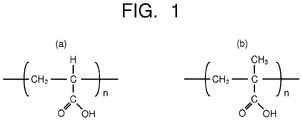
- a base resin forming the resin of the photoresist is polyacrylic acid ( Fig. 1(a) ) or polymethacrylic acid ( Fig. 1(b) ) illustrated in Fig. 1 .
- an about several 10% unit in which a carboxylic acid portion of polyacrylic acid or polymethacrylic acid is substituted by a protecting group is introduced into a polymer chain.
- An introduction amount of the unit substituted by the protecting group is preferably not less than 10 mol% nor more than 50 mol% of the polymer chain.
- the exposure causes the photo acid generator to generate an acid, and the acid serves as a catalyst to remove the protecting group, so that carboxylic acid is generated. Consequently, the resin becomes soluble in a developing solution.
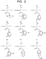
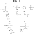
- Examples of the unit in which a group serving as the protecting group is introduced are illustrated in Fig. 2 and Fig. 3 , taking polymethacrylic acid as an example. Only difference in the case of polyacrylic acid is that the methyl group bonded to C of a main chain is replaced by hydrogen, and the other structure is the same.
- Polyacrylic acid and polymethacrylic acid have characteristics of being higher in etching resistance than other resins.
- polyacrylic acid and polymethacrylic acid have a disadvantage of low adhesion. It is effective to introduce a lactone into the resin for the purpose of improving hydrophilic properties of polyacrylic acid and polymethacrylic acid to enhance their adhesion and for the purpose of improving a dissolution contract at the time of the developing.
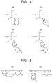
- Fig. 4 illustrates examples of a unit having a lactone copolymerized with polyacrylic acid or polymethacrylic acid.
- a second example of the resin include alternating copolymers of cycloolefin-maleic anhydride (COMA) illustrated in Fig. 5.
- Fig. 5(a) is an example where cycloolefin is norbornane
- Fig. 5(b) is an example where cycloolefin is tetracyclododecane.
- R is a protecting group. The protecting group R is removed by the acid generated from the photo acid generator, so that carboxylic acid is generated, and the resin becomes soluble in the developing solution.
- Fig. 6 illustrates examples of the protecting group R in COMA.
- a COMA-based resin has a high hydrophilic property and has good affinity with an oxide film. Further, it has a high dissolution contrast at the time of the developing. However, the COMA-based resin is low in etching resistance, and in addition, it is readily hydrolyzed because of an anhydride ring that it contains, and thus some measure needs to be taken for its preservation stability. Incidentally, since graphene itself has a high etching property, very high etching resistance is not required.
- a third example of the resin is polycycloolefin whose main chain is formed of cycloolefin as illustrated in Fig. 7 .
- cycloolefin include norbornane illustrated in Fig. 7(a) and cyclododecane illustrated in Fig. 7(b) . They each have carboxylic acid, and part thereof is a substituent (-COOR) substituted by a protecting group.
- Polycycloolefin contains a unit having the substituent (-COOR) in which part of carboxylic acid is substituted by the protecting group. In this case, R is the protecting group, and the protecting group R is removed by the acid generated from the photo acid generator, as in the other resins.
- the protecting group R in polycycloolefin include the same groups as those of the protecting group R in COMA illustrated in Fig. 6 .
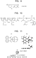
- Examples of a fourth example of the resin include vinyl ether-maleic anhydride copolymers (VEMA) illustrated in Fig. 8.
- Fig. 8(a) illustrates a basic structure of VEMA.
- a ternary compound system in which a polyacrylic unit is introduced to VEMA for the purpose of improving etching resistance may be used ( Fig. 8(b) ).
- portions corresponding to an R1 group and an R2 group are protecting groups. Heating in the presence of an acid removes the protecting group R1 to convert a vinyl ether portion into alcohol. The heating removes the protecting group R2 to convert an acrylic acid portion into carboxylic acid.
- Fig. 9 illustrates another example of a vinyl ether-maleic anhydride copolymer portion.
- VEMA has a high hydrophilic property and has good affinity with an oxide film. Similarly to the COMA-based resin, it requires some measure for etching resistance and preservation stability.
- the resin systems constituting the resin of the photosensitive composition have their own merits and demerits and thus it is preferable that they are appropriately selected for use according to the intended use or the like. Further, in order to compensate for the demerits of the resin systems, it is also possible to use a hybrid polymer in which a plurality of resin systems are combined. For example, as illustrated in Fig. 10 , a hybrid resin of a methacrylic resin that contains a polyacrylic acid-based unit, a polycycloolefin unit, and a maleic anhydride unit, a COMA-based resin, and a polycycloolefin resin, is also usable, for instance.
- the photo acid generator is a component that generates an acid when absorbing exposure light.
- the exposure light is light with a wavelength of not less than 300 nm not more than 500 nm (a g-line (436 nm wavelength) or an i-line (365 nm wavelength) of a halogen lamp or a mercury lamp), it is effective to have a naphthalene ring.
- the exposure light is KrF excimer laser light (248 nm wavelength)
- it is effective to have a benzene ring.
- an aromatic ring such as a naphthalene ring and a benzene ring is ⁇ - ⁇ stacked with graphene when capable of coming close to the graphene.
- Fig. 11 illustrates an example thereof.
- Fig. 11(a) illustrates an example of the structure of a photo acid generator that absorbs light with a 300 to 500 nm wavelength.
- Fig. 11(b) illustrates the most stable structure that its molecule can take.
- the upper drawing is a view of the molecule seen from above, and the lower drawing is a view of the molecule seen from side.
- the circled portion in Fig. 11(a) is a bulky group.
- the photo acid generator illustrated in Fig. 11 is in the most stable state when the bulky group is present in a direction deviating from a surface made by the naphthalene ring as illustrated in Fig. 11(b) .
- the naphthalene ring is capable of coming close to graphene as illustrated in Fig. 11(c) and accordingly the ⁇ - ⁇ stacking can be formed between the naphthalene ring and the graphene.
- a substance having a naphthalene ring or a benzene ring is used, and in addition, a bulky group is bonded to a carbon of the naphthalene ring or the benzene ring.
- Fig. 12 illustrates a first example of the photo acid generator used in the photoresist of the arrangement.
- Fig. 12(a) is a view illustrating a structural formula of the photo acid generator of the first example and
- Fig. 12(b) is a view illustrating a relation between the aromatic ring and graphene in the photo acid generator of the first example.
- t-butyl groups (the circled portions in Fig. 12(a) ) are bonded as the bulky groups to carbon atoms of the naphthalene ring of the photo acid generator illustrated in Fig. 11 .
- the t-butyl groups each have a carbon atom to which three methyl groups are bonded, that is, have a tertiary carbon atom.
- the t-butyl groups each have a shape protruding from a surface formed by the naphthalene ring. This can prevent the naphthalene ring from coming close to the graphene as illustrated in Fig. 12(b) .
- bonding positions of the t-butyl groups are not limited to the positions illustrated in Fig.
- the t-butyl group only needs to be bonded to at least one carbon atom, preferably two carbon atoms, out of carbon atoms of the naphthalene ring to which imidyl sulfonic acid is not bonded.
- the t-butyl group is a representative example of an organic group having the tertiary carbon, and the tertiary carbon bonded to the carbon of the naphthalene ring or the benzene ring is not limited to that of the t-butyl group.
- the naphthalene ring has an sp 2 bond.
- the photo acid generator of the arrangement has the bulky group deviating from the surface formed by the naphthalene ring, which makes the naphthalene ring floated by steric hindrance to prevent it from coming close to the graphene. As a result, the naphthalene ring does not absorb on the graphene and can be prevented from contaminating the graphene. Since the tertiary carbon of the t-butyl group has an sp 3 bond, the three methyl groups and the carbon of the naphthalene ring take the tetrahedral structure.
- the t-butyl group protrudes from the surface formed by the naphthalene ring, preventing the graphene and the naphthalene ring from coming close to each other. Therefore, it is only necessary that the bulky group has the tertiary carbon and the tertiary carbon is bonded to the naphthalene ring, and the bulky group is not limited to the t-butyl group.
- part of the butyl group may be substituted, and for example, may be fluorinated.
- a bulky group may be further bonded to the tertiary carbon, and an alicyclic group such as an adamantyl group or a norbornene group may be bonded.
- a functional group other than the group having the tertiary carbon like the t-butyl group may be further bonded to the carbon of the naphthalene ring.
- the t-butyl groups are bonded to two carbons of the naphthalene ring respectively to prevent the naphthalene ring from coming close to the graphene, but this structure is not restrictive. It is also possible to prevent the naphthalene ring from coming close to the graphene, by bonding the group (bulky group) having the tertiary carbon such as the t-butyl group to one carbon of the naphthalene ring to thereby prevent the naphthalene ring from being parallel to the graphene. In such a case, the positions of the naphthalene ring having the bulky group and the graphene are arranged as illustrated in Fig.
- Fig. 14 illustrates a photo acid generator in which, instead of the group having the tertiary carbon, a group having sulfur (S) to which two carbons are bonded is introduced to a naphthalene ring, and a positional relation between the group having sulfur and the graphene is same as that between the naphthalene ring having the bulky group and the graphene.
- S sulfur
- Fig. 12 since light to be used is light with a wavelength of not less than 300 nm nor more than 500 nm, the description is given using the photo acid generator having the naphthalene ring, but in a case where KrF excimer light is exposure light, a benzene ring is effective for light absorption. Accordingly, in the case where the KrF excimer light is used as the exposure light, a substance having a benzene ring to which a bulky group such as a group having a tertiary carbon is bonded is effective as the photo acid generator, and in this case, the same effect can be also obtained.
- Fig. 13 illustrates an example of such a photo acid generator. The photo acid generator illustrated in Fig.
- the photo acid generator illustrated in Fig. 13 is made of a cation (cationic portion) and an anion (anionic portion), and the diphenyliodonium ion of the cationic portion has the aforesaid t-butyl group.
- the anionic portion is a PF 6 - ion.
- the bonding position of the t-butyl group is not limited to a para position of the benzene ring of the diphenyliodonium ion. The same effect can be expected as long as the t-butyl group is bonded to at least one carbon of the benzene ring in the diphenyliodonium ion. Considering the steric hindrance, the two benzene rings each preferably have the t-butyl group.
- the group having the tertiary carbon is not limited to the t-butyl group, and since the same effect can be expected as long as at least one carbon of the benzene ring is bonded to the tertiary carbon, part of the methyl group in the butyl group may be substituted or may be, for example, fluorinated.
- a bulky group may be further bonded to the tertiary carbon, and an alicyclic group such as an adamantyl group or a norbornene group may be bonded.
- a functional group other than the group having the tertiary carbon like the t-butyl may further be bonded to the benzene ring.
- the diphenyliodonium ion is taken as an example of the cationic portion of the photo acid generator, but the cationic portion is not limited to this.
- the cationic portion is not limited to this.
- a photo acid generator having a triphenyl sulfonium ion as the cationic portion by bonding a group having a tertiary carbon to the carbon of the benzene ring, it is also possible to obtain the same effect.
- the bulky group whose tertiary carbon is bonded to the carbon of the benzene ring or the naphthalene ring is described as an example.
- the bulky group is not limited to the group having the tertiary carbon, and a secondary carbon of an isopropyl group or an isobutyl group having a side chain and not being straight-chained, a sec-butyl group, an isopentyl group, a sec-pentyl group, a 3-pentyl group, an isohexyl group, or the like may be bonded to the carbon of the benzene ring or the naphthalene ring.
- a primary carbon bonded to an alicyclic group such as an adamantyl group or a norbornene group may be bonded.
- an alicyclic group such as an adamantyl group or a norbornene group
- the bulky group is not limited to the group having the tertiary group, but an isopropyl group or an isobutyl group having a side chain and not being straight-chained, a sec-butyl group, an isopentyl group, a sec-pentyl group, a 3-pentyl group, an isohexyl group, or the like is also usable.
- an alicyclic group such as an adamantyl group or a norbornene group may be used.
- a photo acid generator of a different type from the aforesaid photo acid generator in which the bulky group such as the t-butyl group is bonded to at least one carbon of the naphthalene ring or the benzene ring will be described.
- Fig. 14 illustrates an example thereof.
- the photo acid generator is composed of a cationic portion and an anionic portion.
- the cationic portion of the photo acid generator has a sulfonium ion, and a sulfur (S) atom of the sulfonium ion is bonded to a naphthalene ring.
- a group containing this sulfur bonded to two carbons functions as a bulky group.
- the sulfur is bonded to at least one carbon of the naphthalene ring or the benzene ring and the sulfur is bonded to the two carbons
- Fig. 14(a) illustrates a structure in which two methyl groups are bonded to sulfur. Since the sulfur is an ion (S + ), a structure in which the methyl groups protrude to the outside of a surface formed by the naphthalene ring as illustrated in Fig. 14(b) is stable.
- the upper drawing is a view of a photo acid generator molecule seen from above, and the lower drawing is a view of the photo acid generator molecule seen from side.
- Fig. 14(c) illustrates a conceptual view of this case.
- the structure in which the group protruding to the outside of the naphthalene ring is bonded only to one side of the naphthalene ring also prevents the naphthalene ring and the graphene from coming close to each other.
- the cationic portion has the sulfonium ion, and since the state where the two portions (groups having carbons) bonded to the sulfur and not bonded to the naphthalene ring are oriented to the outside of the naphthalene ring is stable, it is possible to prevent the graphene and the naphthalene ring from coming close to each other.
- the carbons bonded to the sulfur are not limited to the carbons of the methyl groups.
- the groups bonded to the sulfur may be partly substituted methyl groups, for example, fluorinated methyl groups, or may be alkyl groups other than the methyl groups.
- a functional group other than the group containing the sulfur may be further bonded to the naphthalene ring.
- the group having the sulfur to which the two methyl groups are bonded is a substituent of the naphthalene ring, but the substituent is not limited to this.
- the groups bonded to the sulfur may be groups bulkier than the methyl groups.
- a primary carbon bonded to an alicyclic group such as an adamantyl group or a norbornene group may be bonded.
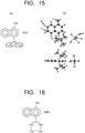
- groups bonded to sulfur are not methyl groups but t-butyl groups.
- Fig. 15(b) illustrates a stable structure, the upper drawing being a view of a photo acid generator molecule seen from above and the lower drawing being a view of the photo acid generator molecule seen from side.
- the two t-butyl groups are arranged symmetrically outside the surface formed by the naphthalene ring to be in the state illustrated in Fig.
- the plural bulky groups (here, the groups each having the tertiary carbon as an example) such as the t-butyl groups are included in the substituent of the naphthalene ring, and accordingly the bulky groups are oriented to the outside of the surface made by the naphthalene ring, which is a stable structure. It is seen that this structure prevents the graphene and the naphthalene ring from coming close to each other.
- the substituent of the naphthalene ring includes not only the sulfonium ion but also the plural bulky groups such as the t-butyl groups, it is possible to prevent the naphthalene ring and the graphene from coming close to each other.
- a case where carbons bonded to sulfur form a ring as illustrated in Fig. 16 is also effective.
- two carbons are bonded to the sulfur bonded to a naphthalene ring and these carbons form a ring structure
- the ring having the four carbons is taken as an example, but the number of the carbons forming the ring structure may be more.
- the photo acid generator contained in the photoresist of the arrangement is formed of a substance having a naphthalene ring or a benzene ring, and for example, has a structure in which at least one carbon atom of the naphthalene ring or the benzene ring is bonded to a tertiary carbon atom, or to a secondary carbon of a group having a side chain, or to a primary carbon bonded to a cyclic group, a structure in which it has a naphthalene ring or a benzene ring, a group bonded to a carbon atom of the naphthalene ring or the benzene ring contains a plurality of bulky groups, in particular, contains a plurality of tertiary carbon atoms, or contains a plurality of groups each having a side chain, or contains a plurality of cyclic groups, or a structure in which at least one carbon atom of the na
- the photo acid generator having such a molecular structure make it possible to inhibit the ⁇ - ⁇ bonding of the naphthalene ring or the benzene ring in the molecular structure to the graphene Therefore, using the photoresist containing such a photo acid generator and containing the aforesaid resin not having the aromatic ring makes it possible to prevent the occurrence of the resist residue on the graphene after the patterning step and reduce performance degradation of the graphene device.
- the cationic portion has the naphthalene ring or the benzene ring.
- the anionic portion SbF 6 - and PF 6 - are cited, but the anionic portion is not limited to these.
- the anionic portion CF 3 SO 3 - , C 4 F 8 SO 3 - , C 8 F 17 SO 3 - , or the like is also usable. These are selected for the purpose of adjusting resist properties such as the intensity of an acid generated after the light irradiation, and various kinds of generally known anionic ions are usable.
- a basic fabrication method of the photoresist of the arrangement is to dissolve the aforesaid resin and photo acid generator in a solvent.
- a solvent propylene glycol monomethyl ether acetate, propylene glycol monomethyl ether, propylene glycol monoethyl ether, propylene glycol monopropyl ether, ⁇ -butyrolactone, 2-heptanone, ethyl lactate, or the like is used. These are selected for the purpose of not only dissolving the resin and the photo acid generator but also obtaining desired coating properties.
- the resin whose ratio is within a 1 to 40% by weight to the solvent is dissolved, and the photo acid generator whose ratio is several %, roughly 5% or less to the resin component is dissolved.
- the photoresist fabricated with such a weight ratio make it possible to obtain favorable resist properties and coating properties.
- the photoresist of the arrangement allows the exposure using light with a wavelength of not less than 300 nm nor more than 500 nm (a g-line (436 nm wavelength) or an i-line (365 nm wavelength) of a mercury lamp light source) or KrF excimer laser light with a 248 nm wavelength, and is prevented from contaminating the graphene, based on the aforesaid combination of the resin and the photo acid generator. This enables the low-cost and efficient fabrication of a high-performance graphene device.
- an alicyclic resin not containing an aromatic ring, or the like is used as its resin in order to reduce the absorption of the exposure light.
- the ArF resist is not sensitive to light of which a wavelength is not less than 300 nm nor more than 500 nm. This is because its photo acid generator does not have the absorption and does not generate an acid. Therefore, this resist is different from the photoresist of the arrangement.
- Figs. 17A to 17C illustrate steps of manufacturing a graphene field-effect transistor (GFET) using the photoresist of the first arrangement, as an example of the method of manufacturing the graphene device.
- the graphene FET (GFET) is used as a high-sensitivity gas sensor, for instance. It should be noted that GFET is an example of the graphene device, and the graphene device is not limited to this.
- a plurality of electrode patterns 12 each having a pair of electrodes 12a, 12b are formed on a Si substrate 11 having a thermal Si oxide film on its front surface side and having back gate electrodes on its rear surface side.
- graphene 13 is transferred onto the Si substrate 11 in a manner that gaps between the pairs of electrodes 12a, 12b in the plural electrode patterns 12 are covered with the graphene.
- the photoresist of the first arrangement is used for trimming (patterning) the graphene 13 illustrated in Fig. 17C .
- the photoresist of the first arrangement is applied on the substrate 11 and is baked at a predetermined temperature (soft bake).
- the baked photoresist film is exposed to light with a wavelength of not less than 300 nm nor more than 500 nm (a g-line (436 nm wavelength) or an i-line (365 nm wavelength) of a mercury lamp light source)) or KrF excimer laser light with a 248 nm wavelength through a photomask.
- the photoresist is baked at a predetermined temperature (post exposure bake), and thereby, the photo acid generator generates an acid. A desired area of the photoresist becomes soluble by the generated acid.
- the photoresist film is developed into a resist pattern using, for example, a tetramethylammonium hydride aqueous solution (TMAH aqueous solution).
- TMAH aqueous solution tetramethylammonium hydride aqueous solution
- etching of the graphene 13 with, for example, O 2 plasma is performed to remove unnecessary portions of the graphene 13.
- the resist pattern (photoresist film) is stripped off using, for example, N,N-dimethylacetamide or N-methylpyrrolidinone (NMP), whereby sheets of patterned graphene 13X as illustrated in Fig. 17C are fabricated.
- NMP N-methylpyrrolidinone
- GFET in which the sheets of thus patterned graphene 13X serve as channels is fabricated.
- the electrodes 12a are sources and the electrodes 12b are drains.
- the ⁇ - ⁇ stacking of the photoresist of the arrangement with the graphene is prevented, it is possible to prevent the residue from occurring after the resist pattern is stripped off. This accordingly reduces performance degradation and so on of GFET due to the resist residue, enabling the low-cost and efficient fabrication of the high-performance GFET.
- the above-described arrangement is the example where the resist pattern is used as the etching mask of the graphene, but the photoresist of the arrangement can be effectively used for other purposes.
- the use of the photoresist of the arrangement also makes it possible to reduce the contamination of the graphene.
- the electrode patterns are sometimes formed after the graphene is first transferred onto the Si oxide film-substrate. Specifically, after the graphene is transferred onto the Si oxide film-substrate, a base film soluble in a developing solution and the photoresist of the arrangement are formed. When the photoresist of the arrangement is heated and thereafter exposed and developed, the base film dissolves in the developing solution after the resist pattern is formed. Using a development condition under which the base film is set back from the photoresist, forms the photoresist into an eaves shape. On such a photoresist, electrode metals (for example, Ni and Au) are deposited in vacuum.
- the photoresist of the arrangement is used to fabricate GFET used in the gas sensor, but a graphene device fabricated by using the manufacturing method of the arrangement is not limited to this.
- the photoresist of the arrangement is applicable to any of various kinds of structures, and the photoresist of the arrangement is usable for trimming the graphene in this case.
- the photoresist of the arrangement is also effective for fabricating graphene sensors such as a sensor in which gas molecules adsorb on graphene of channel portions of GFET and a sensor in which an organic substance that captures gas molecules is installed on graphene of channel portions by being ⁇ - ⁇ bonded to the graphene through a pyrene ring.
- graphene sensors such as a sensor in which gas molecules adsorb on graphene of channel portions of GFET and a sensor in which an organic substance that captures gas molecules is installed on graphene of channel portions by being ⁇ - ⁇ bonded to the graphene through a pyrene ring.
- a substance serving as an electron donor or an electron acceptor such as tetrafluorohydroquinone, tetrafluoro-tetracyanoquinodimethane, or polyethyleneimine or a metal particle of Pt, Pd, Al, or the like is adsorbed.
- a pyrene derivative having a group that reacts with a substance to be sensed is used, and a sensing probe is installed on a graphene surface, by making a pyrene portion of the pyrene derivative ⁇ - ⁇ bonded to the graphene.
- a sensing probe is also formed on a graphene surface. This makes it possible to improve the sensitivity of the sensor and selectively identify a substance to be sensed by the sensing probe.
- the substance to be sensed is not limited to NH 3 and NO 2 which will be described later, but the graphene device is also effective for detecting gas that industrially needs to be detected, such as CO 2 or hydrogen, organic phosphoric acid-based harmful gas such as sarin, tabun, or soman, and a specific substance used for cancer exhalation diagnosis, and if the sensor is a liquid-phase sensor, a virus, for example, a human-infectious influenza virus, or the like. In any of these cases, since graphene with less performance degradation due to contamination can be used as a channel, it is possible to fabricate a graphene FET sensor excellent in performance.
- a graphene device is also used in an optical frequency mixer, an optical communication modulator, a photodetector, an oscillator, and the like as optical communication devices.
- the photoresist of the arrangement is also usable for forming the graphene shape.
- the resist of the present invention is also effective for an electronic device, and is applicable also to a switching element that can achieve an on-off current value ratio of 10 5 .
- the photoresist of the arrangement is effective for a graphene device manufacture having a step of graphene patterning or the like.
- a thermal Si oxide film with a 285 nm thickness is formed on an n-type highly-doped Si substrate.
- An oxide film on a rear surface is stripped off, and metal films, here, 20 nm-thick Ti and 100 nm-thick Ag are deposited to form a back gate electrode.
- a resist pattern serving as an electrode pattern is formed on the Si oxide film using an i-line resist. With the resist pattern used as a mold, electrode metals are deposited in vacuum.
- 10 nm-thick Ni is deposited on the Si oxide film, 20 nm-thick Au is deposited.
- the resultant is immersed in a stripping solution containing N-methylpyrrolidinone (NMP) as a main material, whereby the unnecessary metals together with the resist are lifted off to form the electrode patterns as illustrated in Fig. 17A .
- NMP N-methylpyrrolidinone
- graphene is transferred.
- the graphene one fabricated on a Cu foil by a CVD method is used.
- Polymethyl methacrylate (PMMA) is applied on the graphene surface to protect the surface. Since coarse graphene is on a rear surface of the Cu foil, the coarse graphene is removed with O 2 plasma. Thereafter, the Cu foil with the graphene is immersed in a Cu stripping solution, so that Cu is dissolved. Here, ammonium peroxodisulfate is used.
- the graphene is scooped by the Si substrate on which the electrodes is formed, and the graphene is transferred onto the substrate as illustrated in Fig. 17B .
- the photoresist of the arrangement is used for trimming the graphene.
- a methacrylic resin having the protecting group illustrated in Fig. 2(b) and the photo acid generator illustrated in Fig. 14(a) are used.
- a solvent containing 60% propylene glycol monomethyl ether acetate and 40% propylene glycol monomethyl ether is used, and an amount of the methacrylic resin is adjusted to 10% by weight to the solvent and an amount of the photo acid generator is adjusted to 1% by weight to the resin.
- the resist is applied on the substrate by spin coating and is baked at 130°C for 90 seconds. This is exposed, using a mercury halogen lamp. After exposure, the resist is baked at 130°C for 90 seconds.
- a Cr mask As a mask, a Cr mask is used. This is developed in a tetramethylammonium hydride aqueous solution (TMAH) to be patterned. With the above resist pattern used as a mask, the graphene is etched with O 2 plasma. Thereafter, the resist is stripped off by NMP, whereby graphene FET patterns as illustrated in Fig. 17C are obtained.
- TMAH tetramethylammonium hydride aqueous solution
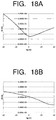
- Fig. 18A illustrates an I-V characteristic (a variation characteristic of a drain current Id when a gate voltage Vg is varied under a constant drain voltage) of the graphene FET fabricated in the example 1.
- Fig. 18B illustrates an I-V characteristic of a graphene FET as a comparative example 1 fabricated in the same manner as in the example 1 except that a commercially available i-line novolac resist is used.
- Graphene displays polarity since holes and electrons serve as carriers, and in its I-V characteristic, a point where Id is the smallest, that is, a Dirac point appears. Inherently, it is neutral when Vg is 0 V.
- the Dirac point is not clearly observed in the graphene FET of the comparative example 1 until Vg becomes 40 V.
- the Dirac point is observed near substantially 0 V as illustrated in Fig. 18A .
- the gradient of the I-V characteristic is proportional to mobility, and in the graphene FET of the example 1, the gradient is larger than in the comparative example 1, from which it is seen that the mobility is large in the graphene FET of the example 1.
- the graphene FET fabricated in this manner is used as a gas sensor
- gas introduction causes charge transfer, so that the I-V characteristic illustrated in Fig. 18A transfers to left or right according to a gas species.
- NO 2 it transfers to right
- NH 3 it transfers to left.
- the gradient of the I-V characteristic is large, an Id variation is large even under the same amount of the left or right transfer. Accordingly, the sensitivity improves. That is, by using the photoresist of the arrangement to fabricate the graphene FET, it is possible to improve sensitivity as a sensor.
- a resin that is the COMA-based resin in Fig. 5(a) and whose substituent R is a t-butyl group, and the photo acid generator illustrated in Fig. 15(a) are dissolved in a solvent containing 60% propylene glycol monomethyl ether acetate and 40% propylene glycol monomethyl ether.
- An amount of the resin is adjusted to 30% by weight to the solvent, and an amount of the photo acid generator is adjusted to 1% by weight to the resin.
- a graphene FET is fabricated in the same manner as in the example 1. In the case, the resist is baked at 90°C for 90 seconds in the soft bake and the post exposure bake.
- the Dirac point is observed at substantially 0 V as in Fig. 18A . Further, since the gradient of the I-V characteristic is larger than that in Fig. 18B , it is confirmed that the mobility is large.
- the hybrid resin illustrated in Fig. 10 and the photo acid generator illustrated in Fig. 12(a) are dissolved in a solvent containing 60% propylene glycol monomethyl ether acetate, 30% propylene glycol monomethyl ether, and 10% ⁇ -butyrolactone.
- An amount of the resin is adjusted to 20% by weight to the solvent, and an amount of the photo acid generator is adjusted to 1% by weight to the resin.
- a graphene FET is fabricated in the same manner as in the example 1.
- the resist is baked at 110°C for 90 seconds in the soft bake and the post exposure bake.
- the Dirac point is observed at substantially 0 V as in Fig. 18A . Further, since the gradient of the I-V characteristic is larger than that in Fig. 18B , it is confirmed that the mobility is large.
- the processes up to the one for transferring the graphene are the same as the example 1.
- the photoresist using the trimming process of the graphene is different from that of the example 1.
- the photoresists using the example 4 and the comparative example 2 are described as follows.
- a methacrylic resin containing a lactone illustrated in Fig. 4(a) and having the protecting group illustrated in Fig. 2(b) is used.
- the monomers are copolymerized so that a unit having the protecting group becomes 20 mol% of the methacrylic resin, and the lactone becomes 5 mol% of the methacrylic resin.
- a solvent containing 60% propylene glycol monomethyl ether acetate and 40% propylene glycol monomethyl ether is used.
- An amount of the photo acid generator is adjusted to 1% by weight to the resin.
- NAI-105 An photo acid generator (NAI-105, manufactured by Midori Kagaku Co., Ltd) of which the naphthalene ring is capable of coming close to graphene is prepared as a photo acid generator of the comparative example 2, and a photo acid generator (NDS-105, manufactured by Midori Kagaku Co., Ltd) of which the naphthalene ring is not capable of coming close to graphene is prepared as a photo acid generator of the example 4.
- NAI-105 has a structure of which hydrogens of the methyl group illustrated in Fig. 11(a) are substituted by fluorines, and the structure is illustrated in Fig. 19(a).
- Fig. 19(b) illustrates a stable structure. In Fig.
- NDS-105 has a cationic portion which is the same as the cationic portion illustrated in Fig. 14(a) and a CF 3 SO 3 - ion as an anionic portion.
- NDS-105 has a structure of which the methyl groups in the cationic portion protrude to the outside of the surface formed by the naphthalene ring, the naphthalene ring is not able to come close to the graphene.
- the graphene FETs are fabricated by using the two types of photoresists having different photo acid generators.
- the process for fabricating the graphene FET by using the photoresist is the same as in the example 1.
- the I-V characteristics of the graphene FETs are measured.
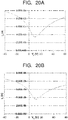
- Figs. 20A and 20B illustrate measured results.
- Fig. 20A illustrates an I-V characteristic of the graphene FET (example 4) fabricated by using NDS-105
- Fig. 20B illustrates an I-V characteristic of the graphene FET (comparative example 2) fabricated by using NAI-105.
- the gradient of the example 4 is larger than that of the comparative example 2.
- the gradient corresponds to the mobility, and the mobility is high so the gradient is large. Therefore, it is thought that the deterioration of the graphene by the resist process is suppressed.
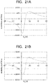
- Figs. 21A and 21B illustrate effective mobility calculated from the gradient of I-V characteristic.
- Fig. 21A illustrates the effective mobility of the example 4 using NDS-105
- Fig. 21B illustrates effective mobility of the comparative example 2 using NAI-105.
- the effective mobility ⁇ is calculated by the following expression (1).
- L is channel length
- W is channel width
- V d drain voltage
- I d drain current
- V g gate voltage
- C ox is ⁇ 0 ⁇ s ⁇ 1/t ( ⁇ 0 : permittivity of vacuum, ⁇ s : relative permittivity of SiO 2 , t: thickness of film).
Landscapes
- Physics & Mathematics (AREA)
- General Physics & Mathematics (AREA)
- Spectroscopy & Molecular Physics (AREA)
- Engineering & Computer Science (AREA)
- Condensed Matter Physics & Semiconductors (AREA)
- Manufacturing & Machinery (AREA)
- Computer Hardware Design (AREA)
- Microelectronics & Electronic Packaging (AREA)
- Power Engineering (AREA)
- Optics & Photonics (AREA)
- Materials For Photolithography (AREA)
- Carbon And Carbon Compounds (AREA)
Applications Claiming Priority (2)
| Application Number | Priority Date | Filing Date | Title |
|---|---|---|---|
| JP2017180938 | 2017-09-21 | ||
| JP2018046574A JP6971896B2 (ja) | 2017-09-21 | 2018-03-14 | グラフェンデバイスの製造方法 |
Publications (1)
| Publication Number | Publication Date |
|---|---|
| EP3460573A1 true EP3460573A1 (de) | 2019-03-27 |
Family
ID=61691371
Family Applications (1)
| Application Number | Title | Priority Date | Filing Date |
|---|---|---|---|
| EP18162333.1A Withdrawn EP3460573A1 (de) | 2017-09-21 | 2018-03-16 | Lichtempfindliche zusammensetzung und verfahren zur herstellung einer graphenvorrichtung |
Country Status (2)
| Country | Link |
|---|---|
| US (2) | US20190086804A1 (de) |
| EP (1) | EP3460573A1 (de) |
Cited By (3)
| Publication number | Priority date | Publication date | Assignee | Title |
|---|---|---|---|---|
| CN111413849A (zh) * | 2020-01-15 | 2020-07-14 | 常州强力先端电子材料有限公司 | 感光性组合物及其制备方法、图案形成方法、应用 |
| WO2021057862A1 (zh) * | 2019-09-25 | 2021-04-01 | 常州强力先端电子材料有限公司 | 能够在i线高产酸的磺酰亚胺类光产酸剂、感光性组合物及其制备方法、图案形成方法、二者的应用 |
| EP4546050A1 (de) | 2023-10-23 | 2025-04-30 | Valstybinis Moksliniu Tyrimu Institutas Fiziniu Ir Technologijos Mokslu Centras | Verfahren zur strukturierung von graphenschichten durch photolithographie zur skalierbaren herstellung von graphenvorrichtungen |
Citations (4)
| Publication number | Priority date | Publication date | Assignee | Title |
|---|---|---|---|---|
| US20090104563A1 (en) * | 2007-10-22 | 2009-04-23 | Tokyo Ohka Kogyo Co., Ltd. | Resist composition, method of forming resist pattern, novel compound, and acid generator |
| US20100209827A1 (en) * | 2009-02-19 | 2010-08-19 | Shin-Etsu Chemical Co., Ltd. | Novel sulfonate and its derivative, photosensitive acid generator, and resist composition and patterning process using the same |
| US20160131976A1 (en) * | 2013-07-17 | 2016-05-12 | Fujifilm Corporation | Resist composition for semiconductor manufacturing process; resist film, resist-coated mask blanks, photomask, and resist patterning method using said resist composition; electronic-device manufacturing method; and electronic device |
| EP3064997A1 (de) * | 2013-10-31 | 2016-09-07 | Fujifilm Corporation | Laminat, kit zur herstellung organischer halbleiter und lackzusammensetzung zur herstellung organischer halbleiter |
Family Cites Families (6)
| Publication number | Priority date | Publication date | Assignee | Title |
|---|---|---|---|---|
| US5302757A (en) * | 1992-09-14 | 1994-04-12 | Eastman Kodak Company | Ultraviolet light sensitive onium salts |
| US6187504B1 (en) * | 1996-12-19 | 2001-02-13 | Jsr Corporation | Radiation sensitive resin composition |
| EP0930541A1 (de) * | 1998-01-16 | 1999-07-21 | JSR Corporation | Strahlungsempfindliche Harzzusammensetzung |
| WO2005061566A1 (ja) * | 2003-12-22 | 2005-07-07 | Lion Corporation | ハイパーブランチポリマー及びその製造方法、並びに該ハイパーブランチポリマーを含有するレジスト組成物 |
| EP3018182A4 (de) * | 2013-07-05 | 2016-12-07 | San-Apro Ltd | Fotosäuregenerator und harzzusammensetzung für fotolithografie |
| KR102295525B1 (ko) * | 2015-01-16 | 2021-08-30 | 삼성전자 주식회사 | 스핀 코팅용 하드 마스크 조성물 |
-
2018
- 2018-03-16 US US15/923,814 patent/US20190086804A1/en not_active Abandoned
- 2018-03-16 EP EP18162333.1A patent/EP3460573A1/de not_active Withdrawn
-
2021
- 2021-01-14 US US17/148,849 patent/US20210141310A1/en not_active Abandoned
Patent Citations (4)
| Publication number | Priority date | Publication date | Assignee | Title |
|---|---|---|---|---|
| US20090104563A1 (en) * | 2007-10-22 | 2009-04-23 | Tokyo Ohka Kogyo Co., Ltd. | Resist composition, method of forming resist pattern, novel compound, and acid generator |
| US20100209827A1 (en) * | 2009-02-19 | 2010-08-19 | Shin-Etsu Chemical Co., Ltd. | Novel sulfonate and its derivative, photosensitive acid generator, and resist composition and patterning process using the same |
| US20160131976A1 (en) * | 2013-07-17 | 2016-05-12 | Fujifilm Corporation | Resist composition for semiconductor manufacturing process; resist film, resist-coated mask blanks, photomask, and resist patterning method using said resist composition; electronic-device manufacturing method; and electronic device |
| EP3064997A1 (de) * | 2013-10-31 | 2016-09-07 | Fujifilm Corporation | Laminat, kit zur herstellung organischer halbleiter und lackzusammensetzung zur herstellung organischer halbleiter |
Cited By (4)
| Publication number | Priority date | Publication date | Assignee | Title |
|---|---|---|---|---|
| WO2021057862A1 (zh) * | 2019-09-25 | 2021-04-01 | 常州强力先端电子材料有限公司 | 能够在i线高产酸的磺酰亚胺类光产酸剂、感光性组合物及其制备方法、图案形成方法、二者的应用 |
| CN111413849A (zh) * | 2020-01-15 | 2020-07-14 | 常州强力先端电子材料有限公司 | 感光性组合物及其制备方法、图案形成方法、应用 |
| CN111413849B (zh) * | 2020-01-15 | 2024-03-01 | 常州强力先端电子材料有限公司 | 感光性组合物及其制备方法、图案形成方法、应用 |
| EP4546050A1 (de) | 2023-10-23 | 2025-04-30 | Valstybinis Moksliniu Tyrimu Institutas Fiziniu Ir Technologijos Mokslu Centras | Verfahren zur strukturierung von graphenschichten durch photolithographie zur skalierbaren herstellung von graphenvorrichtungen |
Also Published As
| Publication number | Publication date |
|---|---|
| US20210141310A1 (en) | 2021-05-13 |
| US20190086804A1 (en) | 2019-03-21 |
Similar Documents
| Publication | Publication Date | Title |
|---|---|---|
| KR101439394B1 (ko) | 산 확산을 이용하는 더블 패터닝 공정에 의한 반도체소자의 미세 패턴 형성 방법 | |
| US8883405B2 (en) | Method for forming pattern | |
| US20210141310A1 (en) | Photosensitive composition and method of manufacturing graphene device | |
| US10777681B2 (en) | Multi-layer photoresist | |
| US8084185B2 (en) | Substrate planarization with imprint materials and processes | |
| Okoroanyanwu et al. | Alicyclic polymers for 193 nm resist applications: Lithographic evaluation | |
| Hayase | Polysilanes for semiconductor fabrication | |
| EP1315044A1 (de) | Resistzusammensetzung und Verfahren zur Herstellung von Halbleiterbauelementen | |
| US20180149976A1 (en) | Lithography Process With Enhanced Etch Selectivity | |
| US11809080B2 (en) | Extreme ultraviolet photoresist with high-efficiency electron transfer | |
| CN108983546A (zh) | 微影方法 | |
| KR101941740B1 (ko) | 반도체 디바이스를 패턴화하는 방법 및 장치 | |
| JP6971896B2 (ja) | グラフェンデバイスの製造方法 | |
| US7566527B2 (en) | Fused aromatic structures and methods for photolithographic applications | |
| US5994007A (en) | Pattern forming method utilizing first insulative and then conductive overlayer and underlayer | |
| JPH02251962A (ja) | 微細パターン形成材料およびパターン形成方法 | |
| US11127592B2 (en) | Photosensitive groups in resist layer | |
| US7282318B2 (en) | Photoresist composition for EUV and method for forming photoresist pattern using the same | |
| JP2002006478A (ja) | 露光用マスクとその製造方法 | |
| Ku et al. | Iodinated underlayer for enhanced chemically amplified resist performance | |
| JP3619037B2 (ja) | パターン形成方法 | |
| EP2985798B1 (de) | Verfahren zum herstellen einer organischen elektronischen vorrichtung | |
| TWI809913B (zh) | 臨界尺寸的測量方法 | |
| Shibayama et al. | EUV sensitive Si containing hard mask (Si-HM) for PTD and NTD process in EUVL | |
| JP2586584B2 (ja) | 微細パターン形成方法 |
Legal Events
| Date | Code | Title | Description |
|---|---|---|---|
| PUAI | Public reference made under article 153(3) epc to a published international application that has entered the european phase |
Free format text: ORIGINAL CODE: 0009012 |
|
| STAA | Information on the status of an ep patent application or granted ep patent |
Free format text: STATUS: REQUEST FOR EXAMINATION WAS MADE |
|
| 17P | Request for examination filed |
Effective date: 20180316 |
|
| AK | Designated contracting states |
Kind code of ref document: A1 Designated state(s): AL AT BE BG CH CY CZ DE DK EE ES FI FR GB GR HR HU IE IS IT LI LT LU LV MC MK MT NL NO PL PT RO RS SE SI SK SM TR |
|
| AX | Request for extension of the european patent |
Extension state: BA ME |
|
| STAA | Information on the status of an ep patent application or granted ep patent |
Free format text: STATUS: THE APPLICATION IS DEEMED TO BE WITHDRAWN |
|
| 18D | Application deemed to be withdrawn |
Effective date: 20190928 |