EP3460510A1 - Fm-cw radar and method for generating fm-cw signal - Google Patents
Fm-cw radar and method for generating fm-cw signal Download PDFInfo
- Publication number
- EP3460510A1 EP3460510A1 EP16902316.5A EP16902316A EP3460510A1 EP 3460510 A1 EP3460510 A1 EP 3460510A1 EP 16902316 A EP16902316 A EP 16902316A EP 3460510 A1 EP3460510 A1 EP 3460510A1
- Authority
- EP
- European Patent Office
- Prior art keywords
- frequency
- signal
- voltage
- processing unit
- signal processing
- Prior art date
- Legal status (The legal status is an assumption and is not a legal conclusion. Google has not performed a legal analysis and makes no representation as to the accuracy of the status listed.)
- Granted
Links
Images



Classifications
-
- G—PHYSICS
- G01—MEASURING; TESTING
- G01S—RADIO DIRECTION-FINDING; RADIO NAVIGATION; DETERMINING DISTANCE OR VELOCITY BY USE OF RADIO WAVES; LOCATING OR PRESENCE-DETECTING BY USE OF THE REFLECTION OR RERADIATION OF RADIO WAVES; ANALOGOUS ARRANGEMENTS USING OTHER WAVES
- G01S7/00—Details of systems according to groups G01S13/00, G01S15/00, G01S17/00
- G01S7/02—Details of systems according to groups G01S13/00, G01S15/00, G01S17/00 of systems according to group G01S13/00
- G01S7/40—Means for monitoring or calibrating
- G01S7/4004—Means for monitoring or calibrating of parts of a radar system
- G01S7/4008—Means for monitoring or calibrating of parts of a radar system of transmitters
-
- G—PHYSICS
- G01—MEASURING; TESTING
- G01S—RADIO DIRECTION-FINDING; RADIO NAVIGATION; DETERMINING DISTANCE OR VELOCITY BY USE OF RADIO WAVES; LOCATING OR PRESENCE-DETECTING BY USE OF THE REFLECTION OR RERADIATION OF RADIO WAVES; ANALOGOUS ARRANGEMENTS USING OTHER WAVES
- G01S13/00—Systems using the reflection or reradiation of radio waves, e.g. radar systems; Analogous systems using reflection or reradiation of waves whose nature or wavelength is irrelevant or unspecified
- G01S13/02—Systems using reflection of radio waves, e.g. primary radar systems; Analogous systems
- G01S13/06—Systems determining position data of a target
- G01S13/08—Systems for measuring distance only
- G01S13/32—Systems for measuring distance only using transmission of continuous waves, whether amplitude-, frequency-, or phase-modulated, or unmodulated
- G01S13/34—Systems for measuring distance only using transmission of continuous waves, whether amplitude-, frequency-, or phase-modulated, or unmodulated using transmission of continuous, frequency-modulated waves while heterodyning the received signal, or a signal derived therefrom, with a locally-generated signal related to the contemporaneously transmitted signal
-
- G—PHYSICS
- G01—MEASURING; TESTING
- G01S—RADIO DIRECTION-FINDING; RADIO NAVIGATION; DETERMINING DISTANCE OR VELOCITY BY USE OF RADIO WAVES; LOCATING OR PRESENCE-DETECTING BY USE OF THE REFLECTION OR RERADIATION OF RADIO WAVES; ANALOGOUS ARRANGEMENTS USING OTHER WAVES
- G01S13/00—Systems using the reflection or reradiation of radio waves, e.g. radar systems; Analogous systems using reflection or reradiation of waves whose nature or wavelength is irrelevant or unspecified
- G01S13/02—Systems using reflection of radio waves, e.g. primary radar systems; Analogous systems
- G01S13/06—Systems determining position data of a target
- G01S13/08—Systems for measuring distance only
- G01S13/32—Systems for measuring distance only using transmission of continuous waves, whether amplitude-, frequency-, or phase-modulated, or unmodulated
- G01S13/34—Systems for measuring distance only using transmission of continuous waves, whether amplitude-, frequency-, or phase-modulated, or unmodulated using transmission of continuous, frequency-modulated waves while heterodyning the received signal, or a signal derived therefrom, with a locally-generated signal related to the contemporaneously transmitted signal
- G01S13/345—Systems for measuring distance only using transmission of continuous waves, whether amplitude-, frequency-, or phase-modulated, or unmodulated using transmission of continuous, frequency-modulated waves while heterodyning the received signal, or a signal derived therefrom, with a locally-generated signal related to the contemporaneously transmitted signal using triangular modulation
-
- G—PHYSICS
- G01—MEASURING; TESTING
- G01S—RADIO DIRECTION-FINDING; RADIO NAVIGATION; DETERMINING DISTANCE OR VELOCITY BY USE OF RADIO WAVES; LOCATING OR PRESENCE-DETECTING BY USE OF THE REFLECTION OR RERADIATION OF RADIO WAVES; ANALOGOUS ARRANGEMENTS USING OTHER WAVES
- G01S7/00—Details of systems according to groups G01S13/00, G01S15/00, G01S17/00
- G01S7/02—Details of systems according to groups G01S13/00, G01S15/00, G01S17/00 of systems according to group G01S13/00
- G01S7/35—Details of non-pulse systems
-
- G—PHYSICS
- G01—MEASURING; TESTING
- G01S—RADIO DIRECTION-FINDING; RADIO NAVIGATION; DETERMINING DISTANCE OR VELOCITY BY USE OF RADIO WAVES; LOCATING OR PRESENCE-DETECTING BY USE OF THE REFLECTION OR RERADIATION OF RADIO WAVES; ANALOGOUS ARRANGEMENTS USING OTHER WAVES
- G01S7/00—Details of systems according to groups G01S13/00, G01S15/00, G01S17/00
- G01S7/02—Details of systems according to groups G01S13/00, G01S15/00, G01S17/00 of systems according to group G01S13/00
- G01S7/40—Means for monitoring or calibrating
-
- G—PHYSICS
- G01—MEASURING; TESTING
- G01S—RADIO DIRECTION-FINDING; RADIO NAVIGATION; DETERMINING DISTANCE OR VELOCITY BY USE OF RADIO WAVES; LOCATING OR PRESENCE-DETECTING BY USE OF THE REFLECTION OR RERADIATION OF RADIO WAVES; ANALOGOUS ARRANGEMENTS USING OTHER WAVES
- G01S7/00—Details of systems according to groups G01S13/00, G01S15/00, G01S17/00
- G01S7/02—Details of systems according to groups G01S13/00, G01S15/00, G01S17/00 of systems according to group G01S13/00
- G01S7/35—Details of non-pulse systems
- G01S7/352—Receivers
- G01S7/358—Receivers using I/Q processing
Definitions
- the present invention relates to an FM-CW radar that uses frequency modulation based on a frequency modulated continuous waves (FM-CW) scheme, and to a method of generating an FM-CW signal that is transmitted by the FM-CW radar.
- FM-CW frequency modulated continuous waves
- An FM-CW radar has the ease of configuration and a relatively low frequency of the baseband that facilitates signal processing, and is thus used commonly these days as a millimeter wave band collision avoidance radar or the like with the aim of reducing cost.
- An FM-CW scheme uses an up-chirp signal that varies a transmit frequency from a low frequency to a high frequency and a down-chirp signal that varies the frequency from a high frequency to a low frequency, and calculates the distance to a target as well as relative velocity with respect to the target on the basis of a sum of peak frequencies and a difference in the peak frequencies of beat signals respectively obtained from the chirp signals.
- transmit/receive modules making up the FM-CW radar require adjustment work in a delivery inspection process due to individual differences and temperature characteristics of voltage control oscillators (hereinafter noted as a "VCO"), and thus hinder reduction of the inspection time in mass production. Because no feedback control performed after shipment, there is a problem in that the radar is unable to respond to a change in the characteristics of the VCO caused by aging or the like.
- VCO voltage control oscillators
- Patent Literature 1 discloses the configuration including: a frequency divider that divides, by the number of divisions N, an output signal from the VCO an oscillating frequency of which varies according to an analog control voltage; a digital phase detector that detects phase information from an output signal of the frequency divider and outputs digital phase information; and a differentiator that differentiates the digital phase information output from the digital phase detector and converts the information into digital frequency information.
- Patent Literature 1 Japanese Patent Application Laid-Open No. 2013-47617
- Patent Literature 1 obtains the frequency information on the basis of the phase information included in the output of the VCO as described above, but does not disclose a specific method of generating the output of the VCO. A conventional technique has thus been unable to properly respond to the change in the characteristics of the VCO caused by aging or the like.
- the present invention has been made in view of the aforementioned circumstances, where an object of the invention is to obtain an FM-CW radar capable of properly responding to a change in the characteristics of a VCO caused by aging or the like, and to obtain a method of generating an FM-CW signal.
- the FM-CW radar includes: a high frequency circuit to receive a reflected wave from a target; and a signal processing unit to convert an analog signal generated by the high frequency circuit into a digital signal and detect at least a distance to the target and velocity of the target, wherein the high frequency circuit includes a voltage control oscillator to generate a frequency-modulated high frequency signal in response to receiving a modulation voltage from the signal processing unit, the signal processing unit includes a look up table to store default modulation control data, and the signal processing unit uses an initial frequency value and an initial voltage value calculated from a voltage-frequency characteristic manifested by application of a default chirp having a linear characteristic, and updates the data stored in the look up table with correction data that is generated by fixing a voltage increment and varying a time increment.
- the FM-CW radar can properly respond to the change in the characteristics of the VCO caused by aging or the like.
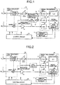
- FIG. 1 is a block diagram illustrating the configuration of an FM-CW radar according to a first embodiment.
- the FM-CW radar according to the first embodiment is an FM-CW radar that uses frequency modulation based on an FM-CW scheme.
- the FM-CW radar is made up of main components including: a high frequency circuit 13 that radiates a transmit signal as a radio wave into space via a transmitting antenna 1 (Tx) and receives, via a receiving antenna 2 (Rx), a reflected wave of the transmitted radio wave that is reflected from a target; a signal processing unit 14 that converts an analog signal output from the high frequency circuit 13 into a digital signal and detects the distance to the target as well as the velocity thereof and, if necessary, the bearing of the target; and a control circuit 12 that controls various control voltages supplied to the high frequency circuit 13.
- the high frequency circuit 13 includes, as basic components: a VCO 4 that receives, as a transmit command, a VCO modulation voltage being a triangular wave voltage signal from the signal processing unit 14 and generates a frequency-modulated high frequency signal; a power distributor 3 that supplies most of the high frequency signal output from the VCO 4 to the transmitting antenna 1 and supplies the rest as a local signal; and a mixer 5 that receives the local signal and uses it to convert the frequency of a received signal from the receiving antenna 2 or, to be specific, down-convert the received signal.
- the components of the high frequency circuit 13 are each formed of a microwave monolithic IC (MMIC).
- a baseband amplifier circuit 6, a prescaler 15, a mixer 17, and a reference frequency generator 18 are provided between the high frequency circuit 13 and the signal processing unit 14. The functions of these components will be described later. Note that the transmitting antenna 1, the receiving antenna 2, the baseband amplifier circuit 6, the control circuit 12, the high frequency circuit 13, the signal processing unit 14, the prescaler 15, the mixer 17, and the reference frequency generator 18 make up a millimeter wave transceiver module.
- the signal processing unit 14 includes: a microcomputer 10 that is a main circuit unit mainly performing transmission processing and measurement processing of the FM-CW radar; a digital-to-analog converter (hereinafter noted as “DAC” as appropriate) 7 that converts the triangular wave voltage signal being the transmit command from the microcomputer 10 into an analog signal and inputs the signal to the VCO 4 of the high frequency circuit 13; an analog-to-digital converter (hereinafter noted as “ADC” as appropriate) 8 that converts a received signal from the baseband amplifier circuit 6 into a digital signal and inputs the signal to the microcomputer 10; and an ADC 16, the function of which will be described in detail later on.
- DAC digital-to-analog converter
- ADC analog-to-digital converter
- the microcomputer 10 includes a look up table (hereinafter noted as "LUT" as appropriate) 9 that stores data of the triangular wave voltage signal being input to the VCO 4.
- the FM-CW radar is further provided with an ambient temperature monitor 11 that monitors the ambient temperature, where a value detected by the ambient temperature monitor 11 is input to the microcomputer 10.
- the control circuit 12 controls the various control voltages supplied to the MMICs in the high frequency circuit 13.
- the microcomputer 10 is provided with a non-volatile memory 19.
- the MMICs in the high frequency circuit 13 vary depending on a production lot.
- the non-volatile memory 19 in the microcomputer 10 thus stores a control voltage value that is individually adjusted and determined for each product of the millimeter wave transceiver module. In the actual operation, the control voltage value is read from the non-volatile memory 19 by the microcomputer 10 and supplied to the MMICs in the high frequency circuit 13 via the control circuit 12.
- the VCO 4 receives the VCO modulation voltage being the triangular wave voltage signal from the signal processing unit 14 and generates an FM-CW signal that is a high frequency signal including an up modulation signal which is shifted up in frequency within a certain period of time, and a down modulation signal which is shifted down in frequency within a certain period of time.
- Most of the FM-CW signal being generated is supplied from the power distributor 3 to the transmitting antenna 1, and the transmitting antenna 1 radiates millimeter waves toward a target.
- the rest of the FM-CW signal namely a portion not supplied to the transmitting antenna 1, is supplied as a local signal to the mixer 5.
- a reflected wave reflected from the target that is captured by the receiving antenna 2 is input to the mixer 5 as a received signal.
- the mixer 5 mixes the received signal from the receiving antenna 2 and the local signal from the power distributor 3 to output a beat signal with a frequency corresponding to a difference in the frequencies of the two signals.
- the beat signal is amplified to an appropriate level in the baseband amplifier circuit 6 and then input to the microcomputer 10 via the ADC 8.
- the microcomputer 10 obtains the distance to the target as well as the relative velocity with respect to the target and, if necessary, the bearing of the target on the basis of the frequency of the input beat signal during each of a period in which the frequency is shifted up and a period in which the frequency is shifted down.
- the frequency of a frequency-divided signal from the VCO 4 is decreased to a fraction of a certain integer by the prescaler 15 and then input to the mixer 17.
- the mixer 17 mixes an output signal from the prescaler 15 and the local signal from the reference frequency generator 18 to output a signal with a frequency corresponding to a difference in the frequencies of the two signals.
- the output signal from the mixer 17 is input to the microcomputer 10 via the ADC 16 and is used to update the data on the triangular wave voltage signal stored in the LUT 9.
- FIG. 2 illustrates another possible configuration not using the mixer 17 or the reference frequency generator 18 used in FIG. 1.
- FIG. 2 illustrates the configuration where the frequency band of a signal input to the ADC 16 is the frequency band of a signal output from the prescaler 15. Although this requires a faster processing clock than the ADC 16 used in FIG. 1 , the advantage of not using the mixer 17 or the reference frequency generator 18 can effectively reduce cost and improve reliability of the millimeter wave transceiver module.
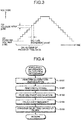
- FIG. 3 is a diagram provided for explaining parameters that make up modulation control data stored in the LUT 9.
- FIG. 4 is a flowchart illustrating the flow of frequency information calculation processing performed by the microcomputer 10.
- FIG. 5 is a block diagram illustrating the calculation flow of the processing illustrated in FIG. 4 when the processing is performed by a dedicated processor.
- FIG. 6 is a flowchart illustrating the flow of correction processing using a polynomial approximation.
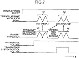
- FIG. 7 is a timing diagram provided for explaining an update of the LUT 9 and transmission processing performed after the update.
- the modulation control data stored in the LUT 9 will be described first with reference to FIG. 3 .
- the modulation control data is formed of a voltage step DV, a starting voltage BV, a time increment DC, and the number of pieces of time data DN.
- the diagram in FIG. 3 has a horizontal axis representing time and a vertical axis representing a voltage value.
- the time increment DC and the number of pieces of time data DN are parameters along the time axis, whereas the starting voltage BV and the voltage step DV are parameters along the voltage axis.
- the voltage step DV is set to an integer multiple of the voltage resolution of the DAC 7 and is basically fixed.
- the DAC 7 with a reference voltage of 5 V and resolution of 10 bit has the voltage resolution of 5/1024 ⁇ 0.00488 V, for example.
- the starting voltage BV is a starting voltage of the modulation control data and is set to an integer multiple of the voltage resolution of the DAC 7, as is the case with the voltage step DV.
- the time increment DC is a duration of a certain voltage value and is set to an integer multiple of the minimum time resolution of the microcomputer 10.
- the time increment DC essentially controls the waveform. Note that the time increment DC has a fixed value in default chirp data that is stored in the LUP 9 as a default.
- the number of pieces of time data DN is a cumulative value of the time increments DC in any single section and indicates the number of pieces of data in the single section.
- the present embodiment forms a desired waveform by fixing the value of the voltage step DV and varying the time increment DC. It is needless to say that the voltage step DV may be variable, not fixed.
- Quadrature demodulation corresponds to processing in step S101 of FIG. 4 as well as processing by a sine function and cosine function generator 31 and multipliers 32a, 32b in FIG. 5 .
- a piece of data sampled from the ADC 16 is subjected to quadrature detection and separated into two signals including an in-phase (I) component and a quadrature (Q) component.
- I component and Q component signals are expressed by the following expression. [Expression 1]
- Q n x n ⁇ cos ⁇ ⁇ ⁇ t ⁇ n
- Filtering corresponds to processing in step S102 of FIG. 4 and processing by low pass filters (hereinafter noted as "LPF") 33a and 33b in FIG. 5 .
- LPF low pass filters
- the filtering is performed to multiply the I signal and the Q signal acquired by the quadrature demodulation in step S101 by corresponding weighting factors according to finite impulse response (FIR) filters, respectively.
- FIR finite impulse response
- the FIR filtering can be expressed by the following expression. Not only the FIR filter but an infinite impulse response (IIR) filter may be used in the filtering.
- Phase calculation corresponds to processing in step S103 of FIG. 4 and processing by an arctangent function calculator 34 in FIG. 5 .
- Frequency calculation corresponds to processing in step S104 of FIG. 4 and processing by a frequency calculator 35 in FIG. 5 .
- step S105 Consideration of a delay time caused by the filter corresponds to processing in step S105 of FIG. 4 .
- the frequency information calculated by the flow of the "frequency information calculation processing" illustrated in FIG. 4 is stored as frequency data with respect to time into the non-volatile memory 19 of the microcomputer 10.
- the modulation control data described with reference to FIG. 3 is already stored in the LUT 9 of the microcomputer 10 as voltage data with respect to time.
- the correction processing using a polynomial approximation in this case uses a polynomial to approximate the relationship between the voltage and the frequency while referring to the "frequency data with respect to time” and the "voltage data with respect to time".
- a piece of modulation data required to obtain linearity of the frequency is generated on the basis of an approximation function obtained by the polynomial approximation, and is applied to the LUT 9 as modulation control data to be output to a next period. That is, the approximation function obtained by the polynomial approximation is used to update the modulation control data stored in the LUT 9.
- FIG. 6 uses, as preconditions, the 10-bit DAC 7 and a quadratic function as a function used in the polynomial approximation.
- Determination of a voltage range corresponds to processing in step S201 of FIG. 6 .
- the frequency is expressed as a quadratic function of the voltage as expressed by the following expression, where a center frequency fc corresponding to a center voltage Vc is obtained to then set a starting frequency fmin as well as a starting voltage Vmin for a required modulation width ⁇ f.
- Setting of a voltage increment corresponds to processing in step S202 of FIG. 6 .
- the voltage step DV is set to a fixed value.
- an initial voltage V 0 is obtained by rounding the starting voltage Vmin obtained by expression (7) to a value that the DAC 7 can have for every voltage increment. Such value then serves as a starting voltage BV.
- An initial frequency f 0 is a frequency corresponding to V 0 .
- the voltage with the initial voltage of Vo is incremented by one step at a time.
- the time obtained is quantized by the minimum time resolution of the microcomputer 10 to be expressed.
- Calculation of a final voltage corresponds to processing in step S205 of FIG. 6 .
- the final voltage is calculated up to where a cumulative time of the time increment data calculated in step S204 does not exceed the prescribed time.
- the number of pieces of the time increments DC acquired is the number of pieces of time data DN.
- the timing diagram in FIG. 7 has a horizontal axis representing time and a vertical axis representing, from the top, an on state of a module power supply, a triangular wave modulation signal, a transmit frequency, a VCO control voltage, and a transmission system control voltage.
- the LUT 9 stores predetermined data as a default of the modulation control data.
- the predetermined data is referred to as default chirp data.
- FIG. 7 indicates the default chirp data by a waveform K1 of the triangular wave modulation signal.
- the frequency of the FM-CW signal transmitted from the transmitting antenna 1 has a waveform as indicated by a waveform K4 with linearity.
- the frequency of the FM-CW signal transmitted from the transmitting antenna 1 has a waveform as indicated by a waveform K2 without linearity.
- the first embodiment converts the frequency-divided signal from the VCO 4 into a digital signal to monitor the signal on a regular basis, and at the same time calculates the frequency information from the phase information of the frequency-divided signal from the VCO 4 (the processing flow in FIG. 4 ).
- a result of the calculation is used to perform the correction processing and calculate voltage data that is required for ensuring the linearity of the transmit frequency (the processing flow in FIG. 6 ).
- the data stored in the LUT 9 is updated to data as indicated by a waveform K3, which is then applied to the waveform K2 to be able to generate the FM-CW signal that has the waveform with linearity as indicated by the waveform K4.
- the FM-CW signal is not transmitted until a first round of the update of the LUT 9 is completed by calculating the frequency information and performing the correction processing.
- the frequency calculation and correction processing are performed after turning on the module power supply and then the VCO control voltage as illustrated in FIG. 7 , whereas transmission of the FM-CW signal can be inhibited by keeping the transmission system control voltage off.
- the transmission system control voltage may be turned on in synchronization with the update of the LUT 9 to enable transmission of the FM-CW signal quickly after the update of the LUT 9.
- the first embodiment calculates the frequency information from the phase information of the frequency-divided signal output from the VCO 4, and updates the data stored in the LUT 9 with correction data that is generated by using the result of the calculation, whereby the radar can properly respond to the change in the characteristics of the VCO caused by aging or the like.
- the ability to properly respond to the change in the characteristics of the VCO allows a reduction in the inspection time required in a delivery inspection process as well as construction of a mechanism of feedback control after the shipment, thereby allowing the VCO correction to be performed with higher accuracy.
- the first embodiment has described the calculation processing in which the V-f curve is approximated by the quadratic function as the correction processing using the polynomial approximation. That is, the first embodiment has described the method of directly calculating the initial voltage value using the quadratic function.
- a second embodiment proposes a method in which the V-f curve can be approximated by a third-order or higher polynomial or another function including an exponential function by using a solution based on an iterative method with the use of an approximate solution.
- FIG. 8 is a flowchart illustrating processing that calculates the initial frequency value and the initial voltage value using a cubic function. The entire processing flow illustrated in FIG. 8 corresponds to step S203 illustrated in FIG. 6 .
- FIG. 9 is a diagram illustrating the waveform of a default chirp.
- FIG. 10 is a diagram illustrating the waveform of a V-f characteristic.
- FIG. 11 is a diagram illustrating a desired t-f characteristic.
- FIG. 12 is a diagram illustrating an applied voltage at the time of correction for obtaining the desired t-f characteristic. Note that a basic configuration is identical or equivalent to the configuration of the first embodiment illustrated in FIG. 1 or 2 , and thus a description of a specific configuration will be omitted.
- the default chirp having a linear characteristic as illustrated in FIG. 9 is applied (step S301).
- the default chirp data is stored in the LUT 9 as described above.
- the V-f characteristic as illustrated in FIG. 10 is manifested by the application of the default chirp, whereby a curve representing the V-f characteristic, that is, the V-f curve, is obtained (step S302).
- step S302 the V-f curve obtained in step S302 is approximated by a cubic function as expressed below (step S303).
- an initial frequency value fmin is determined (step S304). Specifically, the initial frequency value f min can be determined with the voltage of 2.5V defined as the center frequency and ⁇ 200 MHz as the modulation bandwidth, for example.
- V 0 1 as an approximate solution of an initial voltage value V min .
- the initial voltage value V min is obtained by performing iterative calculation according to expression (14) above (step S305).
- the initial voltage value V min practically converges to a desired value by repeating the calculation about five times.
- step S306 time increment data is calculated.
- the idea of the processing in step S306 is equivalent to the processing in step S204 illustrated in FIG. 6 . Although the description is redundant, the processing will be described below because the function is different from that in the description made with reference to FIG. 6 .
- ⁇ is the slope of frequency (GHz/ ⁇ s) and can be obtained from the modulation width and the modulation time. Moreover, the initial frequency value f min may be substituted into ⁇ .
- the voltage increment is thereafter changed step by step starting from the initial voltage value V min obtained in step S305 above. At this time, time data corresponding to the voltage increment changed step by step, that is, the time increment data, is obtained.
- the time increment data obtained here is applied to the LUT 9 as modulation control data to be output in a next period. That is, the function approximated by the cubic function is used to update the modulation control data stored in the LUT 9.
- the subsequent processing is the same as that described in the first embodiment and thus will not be described.
- the second embodiment uses the initial frequency value and the initial voltage value calculated from the V-f characteristic manifested by the application of the default chirp having the linear characteristic and updates the data stored in the LUT 9 with the correction data generated by fixing the voltage increment and varying the time increment, thereby being able to properly respond to a change in the characteristics of the VCO caused by aging or the like.
- the ability to properly respond to the change in the characteristics of the VCO allows a reduction in the inspection time required in a delivery inspection process as well as construction of a feedback control mechanism after shipment, thereby allowing the VCO correction to be performed with high accuracy.
- the LUT 9 is updated by the combination of the frequency calculation processing based on the phase calculation and the correction processing using the polynomial approximation.
- correction processing based on time error calculation is substituted for second and subsequent rounds of updating the LUT 9. Note that a basic configuration is identical or equivalent to the configuration of the first embodiment illustrated in FIG. 1 or 2 , and thus a description of a specific configuration will be omitted.
- FIG. 13 is a flowchart illustrating the flow of the correction processing based on time error calculation performed by a microcomputer 10.
- FIG. 14 is a diagram provided for explaining the concept of the "correction processing based on time error calculation”.
- f ideal represents the ideal frequency line
- f detect represents the frequency data calculated by the flow of FIG. 4
- ⁇ represents a theoretical slope value of the frequency obtained from a modulation width and prescribed time.
- FIG. 14 illustrates an image of such calculation, where an arrow component between the waveform of the frequency data f detect indicated by a solid waveform and the waveform of the ideal frequency line f ideal is calculated as the error, the arrow component corresponding to a difference between the waveforms along a time axis.
- Correction of time increment data corresponds to processing in step S402 of FIG. 13 .
- a time increment DC is corrected by using the error from the ideal frequency line that is calculated by expression (18).
- the beginning of the data range is denoted as k-th
- the time increment DC after correction can be obtained by the following expression.
- DC (k) represents k-th data before correction
- ⁇ t (k) represents an error component obtained by using DC (k)
- DC' (k) represents k-th data after correction
- DC (k+1) represents (k+1)-th data before correction
- ⁇ t (k+1) represents an error component obtained by using DC (k+1)
- DC' (k+1) represents (k+1)-th data after correction.
- the LUT 9 of the third embodiment is updated as follows according to the flow of FIG. 13 .
- a frequency characteristic of default chirp data is subjected to a polynomial approximation (the quadratic approximation in the aforementioned example) and, from a result of the approximation, a voltage table required to secure linearity is calculated.
- a time error with respect to the ideal frequency line is calculated according to the flow in FIG. 13 instead of using the polynomial approximation, and then the time error is used to correct each time data.
- the third embodiment as described above is adapted to calculate, as the error, the difference along the time axis between the calculated frequency information data and the waveform data of the ideal frequency line, and use the calculated error to perform the correction along the time axis to thus be able to obtain an effect similar to that of the first embodiment.
- an indication of a change in characteristics of a VCO caused by a change in ambient temperature is perceived to result in an additional function of detecting an abnormality in a transmit frequency of an FM-CW radar and issuing an alarm and an error.
- a basic configuration is identical or equivalent to the configuration of the first embodiment illustrated in FIG. 1 or 2 , and thus a description of a specific configuration will be omitted.
- FIG. 15 is a table illustrating the image of data stored in a non-volatile memory 19 of a microcomputer 10.
- FIG. 16 is a flowchart illustrating the flow of "alarm processing” according to the fourth embodiment.
- FIG. 17 is a flowchart illustrating the flow of "abnormality determination processing” according to the fourth embodiment.
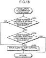
- FIG. 18 is a flowchart illustrating the flow of singularity determination processing according to the fourth embodiment.
- An ambient temperature monitor 11 monitors the ambient temperature of a transceiver module on a regular basis. Temperature data obtained by the ambient temperature monitor 11 is stored in the non-volatile memory 19 along with the transmit frequency that is a frequency of a transmit signal of an FM-CW signal.
- step S501 it is first determined whether or not the transmit frequency falls within a preset tolerance.
- the transmit frequency falling outside the preset tolerance leads to a determination that there is an indication of deterioration, and an alarm is issued to a host control unit (step S502). No alarm is issued if the transmit frequency falls within the present tolerance (Yes in step S501).
- the non-volatile memory 19 stores the transmit frequency information along with the ambient temperature data, thereby allowing one to check whether the transmit frequency deviates from a prescribed value and, in short, allowing one to issue the alarm to the host control unit.
- the non-volatile memory can store a limited number of data and may thus hold data at predetermined temperature intervals and, when not holding data on a temperature concerned, obtain a value of the temperature concerned by a linear approximation.
- the processing flow in FIG. 16 determines whether or not the frequency of the transmit signal falls within the tolerance, whereas a processing flow in FIG. 17 may be executed to determine compliance with the Radio Act. Note that the processing flows in FIGS. 16 and 17 can coexist.
- a transmit frequency Max that is an upper limit of the transmit frequency stipulated by the Radio Act
- a transmit frequency Min that is a lower limit of the transmit frequency being stipulated
- a modulation width of a transmit radar signal are stored in the non-volatile memory 19 together with the temperature data obtained by the ambient temperature monitor 11, as illustrated in FIG. 15 .
- step S601 it is first determined whether or not the transmit frequency falls within the range defined by the upper and lower limits (step S601).
- the transmit frequency falling outside the range defined by the upper and lower limits (No in step S601) leads to a determination that an abnormality is generated, and an error is issued to the host control unit (S603).
- step S602 it is further determined whether or not a modulation bandwidth of the FM-CW signal falls within a range defined by an upper limit. Then if the modulation bandwidth falls outside the range defined by the upper limit (No in step S602), an error is output to the host control unit (step S603).
- the processing flow of FIG. 18 may be executed in addition to the processing flows of FIGS. 16 and 17 . Note that the processing flows of FIGS. 16 to 18 can coexist.
- step S701 it is first checked whether the transmit frequency Min has a temperature singularity (step S701), and, if a singularity is found (No in step S701), an alarm is issued to the host control unit (step S703). Even if the transmit frequency Min has no temperature singularity (Yes in step S701), it is further checked whether the transmit frequency Max has a temperature singularity (step S702) so that an alarm is issued to the host control unit (step S703) if a singularity is found (No in step S702).
- the purpose of the singularity here is to check whether or not the signal behaves differently at a specific temperature. Obtaining information on the singularity has an effect of facilitating a search for a failure when a problem occurs and contributing to improvement in reliability of the device.
- the ambient temperature of the transceiver module including a high frequency circuit 13 is monitored and stored into the non-volatile memory 19 along with the transmit frequency of the FM-CW signal, whereby an effect that the alarm processing, the abnormality determination processing and the singularity determination processing can be performed is obtained in addition to the effect of the first embodiment.
- the processing in the first embodiment may be combined with the processing in the third embodiment, for example.
- the processing in the first embodiment may be combined with the processing in the fourth embodiment, or the processing in the third embodiment may be combined with the processing in the fourth embodiment.
- the processing in the first to fourth embodiments may all be combined.
- Tx transmitting antenna
- Rx receiving antenna
- Rx receiving antenna
- 3 power distributor 5, 17 mixer
- 6 baseband amplifier circuit 7 digital-to-analog converter (DAC), 8, 16 analog-to-digital converter (ADC), 9 look up table (LUT)
- 10 microcomputer 11 ambient temperature monitor, 12 control circuit, 13 high frequency circuit, 14 signal processing unit, 15 prescaler, 18 reference frequency generator, 19 non-volatile memory, 31 sine function generator, 32a, 32b multiplier, 34 arctangent function calculator, 35 frequency calculator.
Landscapes
- Engineering & Computer Science (AREA)
- Radar, Positioning & Navigation (AREA)
- Remote Sensing (AREA)
- Computer Networks & Wireless Communication (AREA)
- Physics & Mathematics (AREA)
- General Physics & Mathematics (AREA)
- Signal Processing (AREA)
- Radar Systems Or Details Thereof (AREA)
Abstract
Description
- The present invention relates to an FM-CW radar that uses frequency modulation based on a frequency modulated continuous waves (FM-CW) scheme, and to a method of generating an FM-CW signal that is transmitted by the FM-CW radar.
- An FM-CW radar has the ease of configuration and a relatively low frequency of the baseband that facilitates signal processing, and is thus used commonly these days as a millimeter wave band collision avoidance radar or the like with the aim of reducing cost.
- An FM-CW scheme uses an up-chirp signal that varies a transmit frequency from a low frequency to a high frequency and a down-chirp signal that varies the frequency from a high frequency to a low frequency, and calculates the distance to a target as well as relative velocity with respect to the target on the basis of a sum of peak frequencies and a difference in the peak frequencies of beat signals respectively obtained from the chirp signals.
- On the other hand, transmit/receive modules making up the FM-CW radar require adjustment work in a delivery inspection process due to individual differences and temperature characteristics of voltage control oscillators (hereinafter noted as a "VCO"), and thus hinder reduction of the inspection time in mass production. Because no feedback control performed after shipment, there is a problem in that the radar is unable to respond to a change in the characteristics of the VCO caused by aging or the like.
- Note that
Patent Literature 1 discloses the configuration including: a frequency divider that divides, by the number of divisions N, an output signal from the VCO an oscillating frequency of which varies according to an analog control voltage; a digital phase detector that detects phase information from an output signal of the frequency divider and outputs digital phase information; and a differentiator that differentiates the digital phase information output from the digital phase detector and converts the information into digital frequency information. - Patent Literature 1: Japanese Patent Application Laid-Open No.
2013-47617 -
Patent Literature 1 obtains the frequency information on the basis of the phase information included in the output of the VCO as described above, but does not disclose a specific method of generating the output of the VCO. A conventional technique has thus been unable to properly respond to the change in the characteristics of the VCO caused by aging or the like. - The present invention has been made in view of the aforementioned circumstances, where an object of the invention is to obtain an FM-CW radar capable of properly responding to a change in the characteristics of a VCO caused by aging or the like, and to obtain a method of generating an FM-CW signal.
- To solve the above problem and achieve an object, there is provided an FM-CW radar using frequency modulation based on an FM-CW scheme. The FM-CW radar according to the present invention includes: a high frequency circuit to receive a reflected wave from a target; and a signal processing unit to convert an analog signal generated by the high frequency circuit into a digital signal and detect at least a distance to the target and velocity of the target, wherein the high frequency circuit includes a voltage control oscillator to generate a frequency-modulated high frequency signal in response to receiving a modulation voltage from the signal processing unit, the signal processing unit includes a look up table to store default modulation control data, and the signal processing unit uses an initial frequency value and an initial voltage value calculated from a voltage-frequency characteristic manifested by application of a default chirp having a linear characteristic, and updates the data stored in the look up table with correction data that is generated by fixing a voltage increment and varying a time increment.
- According to the present invention, the FM-CW radar can properly respond to the change in the characteristics of the VCO caused by aging or the like.
-
-
FIG. 1 is a block diagram illustrating the configuration of an FM-CW radar according to a first embodiment. -
FIG. 2 is a block diagram illustrating the configuration of the FM-CW radar according to the first embodiment, where some components are omitted. -
FIG. 3 is a diagram provided for explaining parameters that make up modulation control data stored in an LUT. -
FIG. 4 is a flowchart illustrating the flow of frequency information calculation processing performed by a microcomputer. -
FIG. 5 is a block diagram illustrating the calculation flow of the processing illustrated inFIG. 4 when the processing is performed by a dedicated processor. -
FIG. 6 is a flowchart illustrating the flow of correction processing using a polynomial approximation. -
FIG. 7 is a timing diagram provided for explaining an update of the LUT and transmission processing performed after the update. -
FIG. 8 is a flowchart illustrating processing that calculates an initial frequency value and an initial voltage value using a cubic function. -
FIG. 9 is a diagram illustrating the waveform of a default chirp. -
FIG. 10 is a diagram illustrating the waveform of a V-f characteristic. -
FIG. 11 is a diagram illustrating a desired t-f characteristic. -
FIG. 12 is a diagram illustrating an applied voltage at the time of correction for obtaining the desired t-f characteristic. -
FIG. 13 is a flowchart illustrating the flow of correction processing based on time error calculation performed by a microcomputer. -
FIG. 14 is a diagram provided for explaining the concept of the correction processing based on the time error calculation. -
FIG. 15 is a table illustrating an image of data stored in a non-volatile memory of the microcomputer. -
FIG. 16 is a flowchart illustrating the flow of alarm processing according to a fourth embodiment. -
FIG. 17 is a flowchart illustrating the flow of abnormality determination processing according to the fourth embodiment. -
FIG. 18 is a flowchart illustrating the flow of singularity determination processing according to the fourth embodiment. - An FM-CW radar and a method of generating an FM-CW signal according to an embodiment of the present invention will now be described in detail with reference to the drawings. Note that the present invention is not to be limited by the following embodiment.
-
FIG. 1 is a block diagram illustrating the configuration of an FM-CW radar according to a first embodiment. The FM-CW radar according to the first embodiment is an FM-CW radar that uses frequency modulation based on an FM-CW scheme. As illustrated inFIG. 1 , the FM-CW radar is made up of main components including: ahigh frequency circuit 13 that radiates a transmit signal as a radio wave into space via a transmitting antenna 1 (Tx) and receives, via a receiving antenna 2 (Rx), a reflected wave of the transmitted radio wave that is reflected from a target; asignal processing unit 14 that converts an analog signal output from thehigh frequency circuit 13 into a digital signal and detects the distance to the target as well as the velocity thereof and, if necessary, the bearing of the target; and acontrol circuit 12 that controls various control voltages supplied to thehigh frequency circuit 13. - The
high frequency circuit 13 includes, as basic components: a VCO 4 that receives, as a transmit command, a VCO modulation voltage being a triangular wave voltage signal from thesignal processing unit 14 and generates a frequency-modulated high frequency signal; a power distributor 3 that supplies most of the high frequency signal output from the VCO 4 to the transmittingantenna 1 and supplies the rest as a local signal; and amixer 5 that receives the local signal and uses it to convert the frequency of a received signal from thereceiving antenna 2 or, to be specific, down-convert the received signal. The components of thehigh frequency circuit 13 are each formed of a microwave monolithic IC (MMIC). - A baseband amplifier circuit 6, a
prescaler 15, amixer 17, and areference frequency generator 18 are provided between thehigh frequency circuit 13 and thesignal processing unit 14. The functions of these components will be described later. Note that the transmittingantenna 1, thereceiving antenna 2, the baseband amplifier circuit 6, thecontrol circuit 12, thehigh frequency circuit 13, thesignal processing unit 14, theprescaler 15, themixer 17, and thereference frequency generator 18 make up a millimeter wave transceiver module. - The
signal processing unit 14 includes: amicrocomputer 10 that is a main circuit unit mainly performing transmission processing and measurement processing of the FM-CW radar; a digital-to-analog converter (hereinafter noted as "DAC" as appropriate) 7 that converts the triangular wave voltage signal being the transmit command from themicrocomputer 10 into an analog signal and inputs the signal to the VCO 4 of thehigh frequency circuit 13; an analog-to-digital converter (hereinafter noted as "ADC" as appropriate) 8 that converts a received signal from the baseband amplifier circuit 6 into a digital signal and inputs the signal to themicrocomputer 10; and anADC 16, the function of which will be described in detail later on. Note that themicrocomputer 10 includes a look up table (hereinafter noted as "LUT" as appropriate) 9 that stores data of the triangular wave voltage signal being input to the VCO 4. The FM-CW radar is further provided with anambient temperature monitor 11 that monitors the ambient temperature, where a value detected by theambient temperature monitor 11 is input to themicrocomputer 10. - Under the control of the
microcomputer 10, thecontrol circuit 12 controls the various control voltages supplied to the MMICs in thehigh frequency circuit 13. Themicrocomputer 10 is provided with anon-volatile memory 19. The MMICs in thehigh frequency circuit 13 vary depending on a production lot. Thenon-volatile memory 19 in themicrocomputer 10 thus stores a control voltage value that is individually adjusted and determined for each product of the millimeter wave transceiver module. In the actual operation, the control voltage value is read from thenon-volatile memory 19 by themicrocomputer 10 and supplied to the MMICs in thehigh frequency circuit 13 via thecontrol circuit 12. - The VCO 4 receives the VCO modulation voltage being the triangular wave voltage signal from the
signal processing unit 14 and generates an FM-CW signal that is a high frequency signal including an up modulation signal which is shifted up in frequency within a certain period of time, and a down modulation signal which is shifted down in frequency within a certain period of time. Most of the FM-CW signal being generated is supplied from the power distributor 3 to the transmittingantenna 1, and the transmittingantenna 1 radiates millimeter waves toward a target. The rest of the FM-CW signal, namely a portion not supplied to the transmittingantenna 1, is supplied as a local signal to themixer 5. - A reflected wave reflected from the target that is captured by the
receiving antenna 2 is input to themixer 5 as a received signal. Themixer 5 mixes the received signal from thereceiving antenna 2 and the local signal from the power distributor 3 to output a beat signal with a frequency corresponding to a difference in the frequencies of the two signals. The beat signal is amplified to an appropriate level in the baseband amplifier circuit 6 and then input to themicrocomputer 10 via the ADC 8. Themicrocomputer 10 obtains the distance to the target as well as the relative velocity with respect to the target and, if necessary, the bearing of the target on the basis of the frequency of the input beat signal during each of a period in which the frequency is shifted up and a period in which the frequency is shifted down. - Here, the frequency of a frequency-divided signal from the VCO 4 is decreased to a fraction of a certain integer by the
prescaler 15 and then input to themixer 17. Themixer 17 mixes an output signal from theprescaler 15 and the local signal from thereference frequency generator 18 to output a signal with a frequency corresponding to a difference in the frequencies of the two signals. The output signal from themixer 17 is input to themicrocomputer 10 via theADC 16 and is used to update the data on the triangular wave voltage signal stored in theLUT 9. -
FIG. 2 illustrates another possible configuration not using themixer 17 or thereference frequency generator 18 used inFIG. 1. FIG. 2 illustrates the configuration where the frequency band of a signal input to theADC 16 is the frequency band of a signal output from theprescaler 15. Although this requires a faster processing clock than theADC 16 used inFIG. 1 , the advantage of not using themixer 17 or thereference frequency generator 18 can effectively reduce cost and improve reliability of the millimeter wave transceiver module. - Main parts of the FM-CW radar according to the first embodiment will now be described with reference to
FIGS. 1 and3 to 7 .FIG. 3 is a diagram provided for explaining parameters that make up modulation control data stored in theLUT 9.FIG. 4 is a flowchart illustrating the flow of frequency information calculation processing performed by themicrocomputer 10.FIG. 5 is a block diagram illustrating the calculation flow of the processing illustrated inFIG. 4 when the processing is performed by a dedicated processor.FIG. 6 is a flowchart illustrating the flow of correction processing using a polynomial approximation.FIG. 7 is a timing diagram provided for explaining an update of theLUT 9 and transmission processing performed after the update. - The modulation control data stored in the
LUT 9 will be described first with reference toFIG. 3 . The modulation control data is formed of a voltage step DV, a starting voltage BV, a time increment DC, and the number of pieces of time data DN. The diagram inFIG. 3 has a horizontal axis representing time and a vertical axis representing a voltage value. The time increment DC and the number of pieces of time data DN are parameters along the time axis, whereas the starting voltage BV and the voltage step DV are parameters along the voltage axis. A more detailed description will now be provided. - The voltage step DV is set to an integer multiple of the voltage resolution of the
DAC 7 and is basically fixed. TheDAC 7 with a reference voltage of 5 V and resolution of 10 bit has the voltage resolution of 5/1024 ≈ 0.00488 V, for example. - The starting voltage BV is a starting voltage of the modulation control data and is set to an integer multiple of the voltage resolution of the
DAC 7, as is the case with the voltage step DV. - The time increment DC is a duration of a certain voltage value and is set to an integer multiple of the minimum time resolution of the
microcomputer 10. The time increment DC essentially controls the waveform. Note that the time increment DC has a fixed value in default chirp data that is stored in theLUP 9 as a default. - The number of pieces of time data DN is a cumulative value of the time increments DC in any single section and indicates the number of pieces of data in the single section.
- Note that in order to increase the accuracy of correction, the present embodiment forms a desired waveform by fixing the value of the voltage step DV and varying the time increment DC. It is needless to say that the voltage step DV may be variable, not fixed.
- The frequency information calculation processing will now be described with reference to
FIGS. 4 and5 . - Quadrature demodulation corresponds to processing in step S101 of
FIG. 4 as well as processing by a sine function andcosine function generator 31 andmultipliers FIG. 5 . Specifically, a piece of data sampled from theADC 16 is subjected to quadrature detection and separated into two signals including an in-phase (I) component and a quadrature (Q) component. These I component and Q component signals are expressed by the following expression.
[Expression 1]
- x(n) : Digital data acquired by sampling
- k : The number of samples
- Δt : Sampling interval
- ω = 2πfLo(fLo : Lo frequency for quadrature demodulation)
- Filtering corresponds to processing in step S102 of
FIG. 4 and processing by low pass filters (hereinafter noted as "LPF") 33a and 33b inFIG. 5 . Note that in the present embodiment, the filtering is performed to multiply the I signal and the Q signal acquired by the quadrature demodulation in step S101 by corresponding weighting factors according to finite impulse response (FIR) filters, respectively. The FIR filtering can be expressed by the following expression. Not only the FIR filter but an infinite impulse response (IIR) filter may be used in the filtering.
[Expression 2]
- Phase calculation corresponds to processing in step S103 of
FIG. 4 and processing by anarctangent function calculator 34 inFIG. 5 . The processing in step S103 is performed to generate an instantaneous phase θ (n) expressed by the following expression.
[Expression 3]
- Frequency calculation corresponds to processing in step S104 of
FIG. 4 and processing by afrequency calculator 35 inFIG. 5 . The processing in step S104 generates an instantaneous frequency f" (n) expressed by the following expression.
[Expression 4]
- Those calculations yield a relationship between the time and the frequency. The acquired frequency is then converted into a value in the 76 to 77 GHz band by the following conversion expression.
[Expression 5]
- fxo: Local oscillator frequency (generated by reference frequency generator)
- N: Division number of prescaler
- The above expression (5) applies to the case where a local oscillator signal frequency fxo of the
reference frequency generator 18 is 19 GHz, or where the frequency-divided signal from the VCO 4 is monitored in the 19 GHz band. - Consideration of a delay time caused by the filter corresponds to processing in step S105 of
FIG. 4 . Regarding the relationship between the time and the frequency acquired through the processing in steps S101 to S104, the processing in step S105 is performed to shift the frequency data while taking into consideration the delay time caused by the FIR filter. Specifically, shift processing as expressed by the following expression is performed in step S105.
[Expression 6]
- Correction processing using a polynomial approximation will now be described. The frequency information calculated by the flow of the "frequency information calculation processing" illustrated in
FIG. 4 is stored as frequency data with respect to time into thenon-volatile memory 19 of themicrocomputer 10. The modulation control data described with reference toFIG. 3 is already stored in theLUT 9 of themicrocomputer 10 as voltage data with respect to time. The correction processing using a polynomial approximation in this case uses a polynomial to approximate the relationship between the voltage and the frequency while referring to the "frequency data with respect to time" and the "voltage data with respect to time". A piece of modulation data required to obtain linearity of the frequency is generated on the basis of an approximation function obtained by the polynomial approximation, and is applied to theLUT 9 as modulation control data to be output to a next period. That is, the approximation function obtained by the polynomial approximation is used to update the modulation control data stored in theLUT 9. - Next, an example of the correction processing using a polynomial approximation will be described with reference to
FIG. 6 . Note that the example inFIG. 6 uses, as preconditions, the 10-bit DAC 7 and a quadratic function as a function used in the polynomial approximation. - Determination of a voltage range corresponds to processing in step S201 of
FIG. 6 . Specifically, the frequency is expressed as a quadratic function of the voltage as expressed by the following expression, where a center frequency fc corresponding to a center voltage Vc is obtained to then set a starting frequency fmin as well as a starting voltage Vmin for a required modulation width Δf.
[Expression 7]
- Setting of a voltage increment corresponds to processing in step S202 of
FIG. 6 . Specifically, the voltage step DV is set to a fixed value. - Setting of an initial voltage and an initial frequency corresponds to processing in step S203 of
FIG. 6 . Specifically, an initial voltage V0 is obtained by rounding the starting voltage Vmin obtained by expression (7) to a value that theDAC 7 can have for every voltage increment. Such value then serves as a starting voltage BV. An initial frequency f0 is a frequency corresponding to V0. The initial frequency is obtained by the following expression.
[Expression 8]
- Calculation of time increment data corresponds to processing in step S204 of
FIG. 6 . Note that α represents a theoretical slope of a frequency obtained from a modulation width and prescribed time.
[Expression 9]
- An expression for calculating time can be expressed by the following expression on the basis of expression (9) and the quadratic approximation (first expression) in expression (7).
[Expression 10]
- Note that the voltage with the initial voltage of Vo is incremented by one step at a time. The time obtained is quantized by the minimum time resolution of the
microcomputer 10 to be expressed. - Calculation of a final voltage corresponds to processing in step S205 of
FIG. 6 . Specifically, the final voltage is calculated up to where a cumulative time of the time increment data calculated in step S204 does not exceed the prescribed time. The number of pieces of the time increments DC acquired is the number of pieces of time data DN. Note that with the initial voltage Vo, a final voltage Ve can be calculated by the following expression.
[Expression 11]
- Next, an update of the
LUT 9 and transmission processing performed after the update according to the first embodiment will be described with reference to a timing diagram inFIG. 7 . The timing diagram inFIG. 7 has a horizontal axis representing time and a vertical axis representing, from the top, an on state of a module power supply, a triangular wave modulation signal, a transmit frequency, a VCO control voltage, and a transmission system control voltage. - The
LUT 9 stores predetermined data as a default of the modulation control data. The predetermined data is referred to as default chirp data.FIG. 7 indicates the default chirp data by a waveform K1 of the triangular wave modulation signal. When there is no change in the characteristics of the VCO 4, the frequency of the FM-CW signal transmitted from the transmittingantenna 1 has a waveform as indicated by a waveform K4 with linearity. On the other hand, when there occurs a change in the characteristics of the VCO 4 due to aging or the like, the frequency of the FM-CW signal transmitted from the transmittingantenna 1 has a waveform as indicated by a waveform K2 without linearity. Because of the above, the first embodiment converts the frequency-divided signal from the VCO 4 into a digital signal to monitor the signal on a regular basis, and at the same time calculates the frequency information from the phase information of the frequency-divided signal from the VCO 4 (the processing flow inFIG. 4 ). A result of the calculation is used to perform the correction processing and calculate voltage data that is required for ensuring the linearity of the transmit frequency (the processing flow inFIG. 6 ). After the processing inFIG. 6 , the data stored in theLUT 9 is updated to data as indicated by a waveform K3, which is then applied to the waveform K2 to be able to generate the FM-CW signal that has the waveform with linearity as indicated by the waveform K4. - The FM-CW signal is not transmitted until a first round of the update of the
LUT 9 is completed by calculating the frequency information and performing the correction processing. In this case, the frequency calculation and correction processing are performed after turning on the module power supply and then the VCO control voltage as illustrated inFIG. 7 , whereas transmission of the FM-CW signal can be inhibited by keeping the transmission system control voltage off. The transmission system control voltage may be turned on in synchronization with the update of theLUT 9 to enable transmission of the FM-CW signal quickly after the update of theLUT 9. - As described above, the first embodiment calculates the frequency information from the phase information of the frequency-divided signal output from the VCO 4, and updates the data stored in the
LUT 9 with correction data that is generated by using the result of the calculation, whereby the radar can properly respond to the change in the characteristics of the VCO caused by aging or the like. The ability to properly respond to the change in the characteristics of the VCO allows a reduction in the inspection time required in a delivery inspection process as well as construction of a mechanism of feedback control after the shipment, thereby allowing the VCO correction to be performed with higher accuracy. - The first embodiment has described the calculation processing in which the V-f curve is approximated by the quadratic function as the correction processing using the polynomial approximation. That is, the first embodiment has described the method of directly calculating the initial voltage value using the quadratic function. On the other hand, instead of directly calculating the initial voltage value, a second embodiment proposes a method in which the V-f curve can be approximated by a third-order or higher polynomial or another function including an exponential function by using a solution based on an iterative method with the use of an approximate solution.
- The present embodiment will describe calculation processing using a cubic function as an example of a function other than the quadratic function with reference to
FIGS. 8 to 12 .FIG. 8 is a flowchart illustrating processing that calculates the initial frequency value and the initial voltage value using a cubic function. The entire processing flow illustrated inFIG. 8 corresponds to step S203 illustrated inFIG. 6 .FIG. 9 is a diagram illustrating the waveform of a default chirp.FIG. 10 is a diagram illustrating the waveform of a V-f characteristic.FIG. 11 is a diagram illustrating a desired t-f characteristic.FIG. 12 is a diagram illustrating an applied voltage at the time of correction for obtaining the desired t-f characteristic. Note that a basic configuration is identical or equivalent to the configuration of the first embodiment illustrated inFIG. 1 or 2 , and thus a description of a specific configuration will be omitted. - First, the default chirp having a linear characteristic as illustrated in
FIG. 9 is applied (step S301). Note that the default chirp data is stored in theLUT 9 as described above. The V-f characteristic as illustrated inFIG. 10 is manifested by the application of the default chirp, whereby a curve representing the V-f characteristic, that is, the V-f curve, is obtained (step S302). - Next, the V-f curve obtained in step S302 is approximated by a cubic function as expressed below (step S303).
[Expression 12]
- At this time, the differentiation of expression (12) as expressed below is also prepared.
[Expression 13]
- Next, an initial frequency value fmin is determined (step S304). Specifically, the initial frequency value fmin can be determined with the voltage of 2.5V defined as the center frequency and ±200 MHz as the modulation bandwidth, for example.
- The initial frequency value fmin obtained in step S304 is substituted into expression (12) to set up a cubic equation as expressed below.
[Expression 14]
- Generally, when finding x that satisfies f (x)=0, a sequence converging to x can be obtained by a recursion formula as expressed below by taking an approximate solution x0.
[Expression 15]
- Experience gives V0=1 as an approximate solution of an initial voltage value Vmin. After that, the initial voltage value Vmin is obtained by performing iterative calculation according to expression (14) above (step S305). The initial voltage value Vmin practically converges to a desired value by repeating the calculation about five times.
- Finally, time increment data is calculated (step S306). The idea of the processing in step S306 is equivalent to the processing in step S204 illustrated in
FIG. 6 . Although the description is redundant, the processing will be described below because the function is different from that in the description made with reference toFIG. 6 . - First, target frequency data for obtaining linearity can be represented by a linear function as follows.
[Expression 16]
- The following expression can be obtained from expressions (12) and (16) above.
[Expression 17]
- α: slope of frequency (GHz/µs) determined by modulation width and modulation time
- β: equal to initial frequency value (fmin)
- In expression (17) above, α is the slope of frequency (GHz/µs) and can be obtained from the modulation width and the modulation time. Moreover, the initial frequency value fmin may be substituted into β. The voltage increment is thereafter changed step by step starting from the initial voltage value Vmin obtained in step S305 above. At this time, time data corresponding to the voltage increment changed step by step, that is, the time increment data, is obtained. The time increment data obtained here is applied to the
LUT 9 as modulation control data to be output in a next period. That is, the function approximated by the cubic function is used to update the modulation control data stored in theLUT 9. The subsequent processing is the same as that described in the first embodiment and thus will not be described. - As described above, the second embodiment uses the initial frequency value and the initial voltage value calculated from the V-f characteristic manifested by the application of the default chirp having the linear characteristic and updates the data stored in the
LUT 9 with the correction data generated by fixing the voltage increment and varying the time increment, thereby being able to properly respond to a change in the characteristics of the VCO caused by aging or the like. The ability to properly respond to the change in the characteristics of the VCO allows a reduction in the inspection time required in a delivery inspection process as well as construction of a feedback control mechanism after shipment, thereby allowing the VCO correction to be performed with high accuracy. - In the first embodiment, the
LUT 9 is updated by the combination of the frequency calculation processing based on the phase calculation and the correction processing using the polynomial approximation. In a third embodiment, correction processing based on time error calculation is substituted for second and subsequent rounds of updating theLUT 9. Note that a basic configuration is identical or equivalent to the configuration of the first embodiment illustrated inFIG. 1 or 2 , and thus a description of a specific configuration will be omitted. - Main parts of an FM-CW radar according to the third embodiment will now be described with reference to
FIGS. 13 and14 .FIG. 13 is a flowchart illustrating the flow of the correction processing based on time error calculation performed by amicrocomputer 10.FIG. 14 is a diagram provided for explaining the concept of the "correction processing based on time error calculation". - Calculation of an error from an ideal frequency line corresponds to processing in step S401 of
FIG. 13 . Specifically, "frequency data with respect to time" is calculated first according to the flow of "frequency information calculation processing" illustrated inFIG. 4 . Then, an error δt (i) between the "frequency data with respect to time" and the ideal frequency line is calculated on the basis of the following expression.
[Expression 18]
- In expression (18), fideal represents the ideal frequency line, and fdetect represents the frequency data calculated by the flow of
FIG. 4 . Moreover, α represents a theoretical slope value of the frequency obtained from a modulation width and prescribed time.FIG. 14 illustrates an image of such calculation, where an arrow component between the waveform of the frequency data fdetect indicated by a solid waveform and the waveform of the ideal frequency line fideal is calculated as the error, the arrow component corresponding to a difference between the waveforms along a time axis. - Correction of time increment data corresponds to processing in step S402 of
FIG. 13 . Specifically, a time increment DC is corrected by using the error from the ideal frequency line that is calculated by expression (18). Where the beginning of the data range is denoted as k-th, the time increment DC after correction can be obtained by the following expression.
[Expression 19]
- In expression (19), DC (k) represents k-th data before correction, δt (k) represents an error component obtained by using DC (k), and DC' (k) represents k-th data after correction. Likewise, DC (k+1) represents (k+1)-th data before correction, δt (k+1) represents an error component obtained by using DC (k+1), and DC' (k+1) represents (k+1)-th data after correction.
- The
LUT 9 of the third embodiment is updated as follows according to the flow ofFIG. 13 . In a first round of updating theLUT 9, a frequency characteristic of default chirp data is subjected to a polynomial approximation (the quadratic approximation in the aforementioned example) and, from a result of the approximation, a voltage table required to secure linearity is calculated. In second and subsequent rounds of updating theLUT 9, a time error with respect to the ideal frequency line is calculated according to the flow inFIG. 13 instead of using the polynomial approximation, and then the time error is used to correct each time data. - The third embodiment as described above is adapted to calculate, as the error, the difference along the time axis between the calculated frequency information data and the waveform data of the ideal frequency line, and use the calculated error to perform the correction along the time axis to thus be able to obtain an effect similar to that of the first embodiment.
- In a fourth embodiment, an indication of a change in characteristics of a VCO caused by a change in ambient temperature is perceived to result in an additional function of detecting an abnormality in a transmit frequency of an FM-CW radar and issuing an alarm and an error. A basic configuration is identical or equivalent to the configuration of the first embodiment illustrated in
FIG. 1 or 2 , and thus a description of a specific configuration will be omitted. - Main parts of the FM-CW radar according to the fourth embodiment will now be described with reference to
FIGS. 15 to 18 .FIG. 15 is a table illustrating the image of data stored in anon-volatile memory 19 of amicrocomputer 10.FIG. 16 is a flowchart illustrating the flow of "alarm processing" according to the fourth embodiment.FIG. 17 is a flowchart illustrating the flow of "abnormality determination processing" according to the fourth embodiment.FIG. 18 is a flowchart illustrating the flow of singularity determination processing according to the fourth embodiment. - An ambient temperature monitor 11 monitors the ambient temperature of a transceiver module on a regular basis. Temperature data obtained by the ambient temperature monitor 11 is stored in the
non-volatile memory 19 along with the transmit frequency that is a frequency of a transmit signal of an FM-CW signal. - According to the flow of the alarm processing in
FIG. 16 , it is first determined whether or not the transmit frequency falls within a preset tolerance (step S501). The transmit frequency falling outside the preset tolerance (No in step S501) leads to a determination that there is an indication of deterioration, and an alarm is issued to a host control unit (step S502). No alarm is issued if the transmit frequency falls within the present tolerance (Yes in step S501). - The
non-volatile memory 19 stores the transmit frequency information along with the ambient temperature data, thereby allowing one to check whether the transmit frequency deviates from a prescribed value and, in short, allowing one to issue the alarm to the host control unit. - Note that the non-volatile memory can store a limited number of data and may thus hold data at predetermined temperature intervals and, when not holding data on a temperature concerned, obtain a value of the temperature concerned by a linear approximation.
- The processing flow in
FIG. 16 determines whether or not the frequency of the transmit signal falls within the tolerance, whereas a processing flow inFIG. 17 may be executed to determine compliance with the Radio Act. Note that the processing flows inFIGS. 16 and 17 can coexist. - In the execution of the processing flow in
FIG. 17 , a transmit frequency Max that is an upper limit of the transmit frequency stipulated by the Radio Act, a transmit frequency Min that is a lower limit of the transmit frequency being stipulated, and a modulation width of a transmit radar signal are stored in thenon-volatile memory 19 together with the temperature data obtained by theambient temperature monitor 11, as illustrated inFIG. 15 . - According to the flow of the abnormality determination processing in
FIG. 17 , it is first determined whether or not the transmit frequency falls within the range defined by the upper and lower limits (step S601). The transmit frequency falling outside the range defined by the upper and lower limits (No in step S601) leads to a determination that an abnormality is generated, and an error is issued to the host control unit (S603). Even when the transmit frequency falls within the range defined by the upper and lower limits (Yes in S601), it is further determined whether or not a modulation bandwidth of the FM-CW signal falls within a range defined by an upper limit (step S602). Then if the modulation bandwidth falls outside the range defined by the upper limit (No in step S602), an error is output to the host control unit (step S603). - It is needless to say that an action such as stopping the output of transmission is taken when the error is issued to the host control unit.
- The processing flow of
FIG. 18 may be executed in addition to the processing flows ofFIGS. 16 and 17 . Note that the processing flows ofFIGS. 16 to 18 can coexist. - In the flow of singularity determination processing illustrated in
FIG. 18 , it is first checked whether the transmit frequency Min has a temperature singularity (step S701), and, if a singularity is found (No in step S701), an alarm is issued to the host control unit (step S703). Even if the transmit frequency Min has no temperature singularity (Yes in step S701), it is further checked whether the transmit frequency Max has a temperature singularity (step S702) so that an alarm is issued to the host control unit (step S703) if a singularity is found (No in step S702). Note that the purpose of the singularity here is to check whether or not the signal behaves differently at a specific temperature. Obtaining information on the singularity has an effect of facilitating a search for a failure when a problem occurs and contributing to improvement in reliability of the device. - Note that although the processing flow of
FIG. 18 performs the singularity determination processing for both the transmit frequency Min and the transmit frequency Max, the above effect can be obtained by performing the singularity determination processing for at least one of the frequencies. - In the fourth embodiment described above, the ambient temperature of the transceiver module including a
high frequency circuit 13 is monitored and stored into thenon-volatile memory 19 along with the transmit frequency of the FM-CW signal, whereby an effect that the alarm processing, the abnormality determination processing and the singularity determination processing can be performed is obtained in addition to the effect of the first embodiment. - The configuration illustrated in the aforementioned embodiment merely illustrates an example of the content of the present invention, and can thus be combined with another known technique or partially omitted and/or modified without departing from the gist of the present invention.
- The processing in the first embodiment may be combined with the processing in the third embodiment, for example. Alternatively, the processing in the first embodiment may be combined with the processing in the fourth embodiment, or the processing in the third embodiment may be combined with the processing in the fourth embodiment. Still alternatively, the processing in the first to fourth embodiments may all be combined.
- 1 transmitting antenna (Tx), 2 receiving antenna (Rx), 3 power distributor, 5, 17 mixer, 6 baseband amplifier circuit, 7 digital-to-analog converter (DAC), 8, 16 analog-to-digital converter (ADC), 9 look up table (LUT), 10 microcomputer, 11 ambient temperature monitor, 12 control circuit, 13 high frequency circuit, 14 signal processing unit, 15 prescaler, 18 reference frequency generator, 19 non-volatile memory, 31 sine function generator, 32a, 32b multiplier, 34 arctangent function calculator, 35 frequency calculator.
Claims (8)
- An FM-CW radar using frequency modulation based on an FM-CW scheme, the FM-CW radar comprising:a high frequency circuit to receive a reflected wave from a target; anda signal processing unit to convert an analog signal generated by the high frequency circuit into a digital signal and detect at least a distance to the target and velocity of the target, whereinthe high frequency circuit includes a voltage control oscillator to generate a frequency-modulated high frequency signal in response to receiving a modulation voltage from the signal processing unit,the signal processing unit includes a look up table to store default modulation control data, andthe signal processing unit uses an initial frequency value and an initial voltage value calculated from a voltage-frequency characteristic manifested by application of a default chirp having a linear characteristic, and updates the data stored in the look up table with correction data that is generated by fixing a voltage increment and varying a time increment.
- The FM-CW radar according to claim 1, wherein the FM-CW radar does not transmit an FM-CW signal until a first round of updating the look up table is completed by calculating the frequency information and performing correction processing.
- The FM-CW radar according to claim 1 or 2, wherein the signal processing unit calculates, as an error, a difference along a time axis between data of the frequency information being calculated and waveform data of an ideal frequency line, and uses the calculated error to perform a correction along the time axis.
- The FM-CW radar according to any one of claims 1 to 3, wherein
the signal processing unit includes a non-volatile memory, and
the signal processing unit monitors ambient temperature of a transceiver module including the high frequency circuit, and stores temperature data obtained by the monitoring into the non-volatile memory along with a transmit frequency of the FM-CW signal. - The FM-CW radar according to claim 4, wherein the signal processing unit uses the temperature data stored in the non-volatile memory to determine whether or not the transmit frequency falls within a preset tolerance, and issues an alarm to a host control unit when the transmit frequency falls outside the tolerance.
- The FM-CW radar according to claim 4, wherein the signal processing unit uses the temperature data stored in the non-volatile memory to determine whether or not the transmit frequency falls within a range defined by an upper limit and a lower limit, or whether or not a modulation bandwidth of the FM-CW signal falls within a range defined by an upper limit, and issues an error to a host control unit when the transmit frequency falls outside the range defined by the upper limit and the lower limit or when the modulation bandwidth falls outside the range defined by the upper limit.
- The FM-CW radar according to claim 4, wherein the signal processing unit uses the temperature data stored in the non-volatile memory to determine whether or not at least one of a lower limit of the transmit frequency and an upper limit of the transmit frequency has a singularity, and issues an alarm to a host control unit when the singularity is determined to exist.
- A method of generating an FM-CW signal transmitted from an FM-CW radar including: a high frequency circuit to include a voltage control oscillator generating a frequency-modulated high frequency signal; and a signal processing unit to convert an analog signal generated by the high frequency circuit into a digital signal and detect at least a distance to a target and velocity of the target, wherein
the signal processing unit includes a look up table to store default modulation control data, and
the FM-CW radar generates the FM-CW signal by executing processing including:a first step of applying a default chirp having a linear characteristic;a second step of calculating an initial frequency value and an initial voltage value from a voltage-frequency characteristic manifested by the application of the default chirp;a third step of calculating time data by using a result of the calculation in the second step, by fixing a voltage increment and varying a time increment; anda fourth step of updating a value stored in the look up table by using the time data calculated in the third step.
Applications Claiming Priority (1)
| Application Number | Priority Date | Filing Date | Title |
|---|---|---|---|
| PCT/JP2016/064497 WO2017199296A1 (en) | 2016-05-16 | 2016-05-16 | Fm-cw radar and method for generating fm-cw signal |
Publications (3)
| Publication Number | Publication Date |
|---|---|
| EP3460510A1 true EP3460510A1 (en) | 2019-03-27 |
| EP3460510A4 EP3460510A4 (en) | 2019-06-26 |
| EP3460510B1 EP3460510B1 (en) | 2021-03-17 |
Family
ID=60326302
Family Applications (1)
| Application Number | Title | Priority Date | Filing Date |
|---|---|---|---|
| EP16902316.5A Active EP3460510B1 (en) | 2016-05-16 | 2016-05-16 | Fm-cw radar and method for generating fm-cw signal |
Country Status (5)
| Country | Link |
|---|---|
| US (1) | US11029389B2 (en) |
| EP (1) | EP3460510B1 (en) |
| JP (1) | JP6647396B2 (en) |
| CN (1) | CN109196375B (en) |
| WO (1) | WO2017199296A1 (en) |
Families Citing this family (12)
| Publication number | Priority date | Publication date | Assignee | Title |
|---|---|---|---|---|
| GB2562412B (en) | 2016-01-07 | 2022-03-16 | Mi Llc | Breaker fluids and methods of use thereof |
| US11490363B2 (en) * | 2018-04-18 | 2022-11-01 | Google Llc | User device-initiated bandwidth request |
| JP7011729B2 (en) * | 2018-09-20 | 2022-02-10 | 京セラ株式会社 | Electronic devices, control methods for electronic devices, and control programs for electronic devices |
| US11204410B2 (en) * | 2019-02-11 | 2021-12-21 | Nxp B.V. | Radar-based communication |
| US12265148B2 (en) | 2019-03-25 | 2025-04-01 | Mitsubishi Electric Corporation | Radar device |
| JP2021001735A (en) * | 2019-06-19 | 2021-01-07 | 旭化成エレクトロニクス株式会社 | Sensor device and sensing method |
| CN111025278B (en) * | 2019-12-31 | 2023-09-01 | 北京中科飞鸿科技股份有限公司 | Radio altimeter |
| JP7657766B2 (en) * | 2020-02-14 | 2025-04-07 | 古野電気株式会社 | Water vapor observation device, water vapor observation system, water vapor observation method, and water vapor observation program |
| WO2021212410A1 (en) * | 2020-04-23 | 2021-10-28 | 华为技术有限公司 | Method and device for controlling radar frequency hopping, radar speed measurement method and radar |
| US11550027B2 (en) | 2020-05-04 | 2023-01-10 | Nxp B.V. | Predistortion technique for joint radar/communication systems |
| US12007465B2 (en) | 2021-10-19 | 2024-06-11 | Nxp B.V. | Radar apparatus and method with content embedded in the radar signal |
| WO2024090071A1 (en) * | 2022-10-25 | 2024-05-02 | ソニーセミコンダクタソリューションズ株式会社 | Ranging device, optical detection device, and signal processing device |
Family Cites Families (31)
| Publication number | Priority date | Publication date | Assignee | Title |
|---|---|---|---|---|
| US4593287A (en) * | 1982-09-30 | 1986-06-03 | The Boeing Company | FM/CW sweep linearizer and method therefor |
| US5172123A (en) | 1985-01-29 | 1992-12-15 | Hercules Defense Electronics, Inc. | Frequency feedback linearizer |
| JPH0718172Y2 (en) | 1989-04-12 | 1995-04-26 | 横河電機株式会社 | Variable frequency signal generator |
| DE10018552A1 (en) | 2000-04-14 | 2001-10-18 | Bosch Gmbh Robert | Detecting and correcting nonlinearities in microwave radar system e.g. for motor vehicle by detecting reference signal during application of test drive voltage and using to correct fm curve |
| KR100395213B1 (en) | 2001-03-22 | 2003-08-21 | 주식회사 버카나와이어리스코리아 | Quadrature Signal Generator and Phase Error Correction Method |
| JP2003232851A (en) | 2002-02-08 | 2003-08-22 | Murata Mfg Co Ltd | Radar and method for adjusting characteristic thereof |
| JP2003294835A (en) | 2002-04-01 | 2003-10-15 | Murata Mfg Co Ltd | Radar |
| KR100462600B1 (en) | 2002-04-02 | 2004-12-20 | 삼성전자주식회사 | Apparatus and method for controlling automatically adjustment of power supply in a plasma display panel drive system |
| JP3915811B2 (en) | 2002-08-26 | 2007-05-16 | 三菱電機株式会社 | Waveform generation program and FM-CW radar device |
| EP1739841B1 (en) | 2004-02-25 | 2016-04-13 | Mitsubishi Denki Kabushiki Kaisha | Waveform generation method, radar device, and oscillator for radar device |
| JP4046293B2 (en) * | 2005-06-03 | 2008-02-13 | 三菱電機株式会社 | Radio radar equipment |
| JP5034306B2 (en) | 2006-04-28 | 2012-09-26 | 富士通株式会社 | Frequency modulation circuit, FM-CW radar apparatus, and communication integrated radar apparatus |
| EP2045616B1 (en) * | 2006-07-21 | 2013-09-11 | Mitsubishi Electric Corporation | Modulation signal generation circuit, transmission/reception module, and radar device |
| EP2600520B1 (en) | 2006-07-21 | 2014-09-10 | Mitsubishi Electric Corporation | Modulation signal generation circuit, transmission/reception module, and radar device |
| JP4983409B2 (en) * | 2007-06-04 | 2012-07-25 | 富士通株式会社 | Phase-locked oscillator and multi-radar system using the same |
| US7898344B2 (en) | 2006-09-12 | 2011-03-01 | Fujitsu Limited | Phase-locked oscillator and multi-radar system using same |
| JP4977443B2 (en) | 2006-10-31 | 2012-07-18 | 日立オートモティブシステムズ株式会社 | Radar apparatus and radar detection method |
| WO2008072481A1 (en) | 2006-12-11 | 2008-06-19 | Murata Manufacturing Co., Ltd. | Radar apparatus |
| JP5185553B2 (en) | 2007-03-20 | 2013-04-17 | 三菱電機株式会社 | Millimeter-wave transceiver module |
| JP4978276B2 (en) | 2007-03-30 | 2012-07-18 | 三菱電機株式会社 | Pulse signal detector |
| EP2184857A4 (en) | 2007-08-28 | 2013-10-16 | Fujitsu Ltd | PHASE LOCKED OSCILLATOR AND RADAR DEVICE |
| JP4975796B2 (en) * | 2009-10-01 | 2012-07-11 | 三菱電機株式会社 | Temperature correction device |
| JP2011082744A (en) | 2009-10-06 | 2011-04-21 | Nec Corp | Voltage-controlled oscillator, and amplitude adjustment method |
| CN101793964A (en) * | 2010-03-09 | 2010-08-04 | 浙江大学 | 60GHz millimeter-wave automotive anti-collision radar device with digitized temperature compensation |
| JP5178761B2 (en) | 2010-03-19 | 2013-04-10 | 株式会社東芝 | FMCW signal generation circuit and radar device |
| JP5586297B2 (en) | 2010-03-29 | 2014-09-10 | 三菱電機株式会社 | Temperature abnormality detection device and millimeter wave radar module |
| JP5670149B2 (en) | 2010-06-09 | 2015-02-18 | 株式会社日立国際電気 | transceiver |
| JP5566974B2 (en) | 2011-08-29 | 2014-08-06 | 株式会社東芝 | Signal generation circuit, oscillation device, radar device |
| KR102038557B1 (en) | 2012-11-07 | 2019-10-30 | 현대모비스 주식회사 | Apparatus and Method for Signal Linearizing of Radar System |
| JP5972203B2 (en) * | 2013-03-25 | 2016-08-17 | 三菱電機株式会社 | FM-CW radar equipment |
| US10585169B2 (en) | 2014-10-03 | 2020-03-10 | Mitsubishi Electric Corporation | Signal generating circuit |
-
2016
- 2016-05-16 CN CN201680085580.6A patent/CN109196375B/en active Active
- 2016-05-16 EP EP16902316.5A patent/EP3460510B1/en active Active
- 2016-05-16 WO PCT/JP2016/064497 patent/WO2017199296A1/en not_active Ceased
- 2016-05-16 JP JP2018517939A patent/JP6647396B2/en active Active
- 2016-05-16 US US16/094,943 patent/US11029389B2/en active Active
Also Published As
| Publication number | Publication date |
|---|---|
| JPWO2017199296A1 (en) | 2018-08-30 |
| EP3460510A4 (en) | 2019-06-26 |
| JP6647396B2 (en) | 2020-02-14 |
| EP3460510B1 (en) | 2021-03-17 |
| CN109196375A (en) | 2019-01-11 |
| US11029389B2 (en) | 2021-06-08 |
| US20190120933A1 (en) | 2019-04-25 |
| WO2017199296A1 (en) | 2017-11-23 |
| CN109196375B (en) | 2023-06-30 |
Similar Documents
| Publication | Publication Date | Title |
|---|---|---|
| EP3460510B1 (en) | Fm-cw radar and method for generating fm-cw signal | |
| EP3260881B1 (en) | Fm-cw radar and fm-cw signal generation method | |
| EP3203260B1 (en) | Signal-generating circuit | |
| US8937572B2 (en) | Signal generator, oscillator, and radar device | |
| US10727848B2 (en) | Phase-locked loop having a multi-band oscillator and method for calibrating same | |
| US20180267159A1 (en) | Signal generator | |
| CN107250833B (en) | Radar apparatus | |
| EP3422044B1 (en) | Frequency modulation circuit, fm-cw radar, and high-speed modulation radar | |
| EP2184857A1 (en) | Phase-locked oscillator and radar device including the same | |
| US11002844B2 (en) | Radar system with internal ramp linearity measurement capability | |
| JP2018185347A (en) | FM-CW radar | |
| US11448742B2 (en) | Radar device | |
| JP2020094931A (en) | Frequency characteristic correcting device and frequency characteristic correction method | |
| JPH0318784A (en) | Fm-cw distance measuring method | |
| US12345559B2 (en) | Fill-level measurement device | |
| CN119716756A (en) | Method and radar MMIC device for determining phase information associated with an RF transmission channel |
Legal Events
| Date | Code | Title | Description |
|---|---|---|---|
| STAA | Information on the status of an ep patent application or granted ep patent |
Free format text: STATUS: THE INTERNATIONAL PUBLICATION HAS BEEN MADE |
|
| PUAI | Public reference made under article 153(3) epc to a published international application that has entered the european phase |
Free format text: ORIGINAL CODE: 0009012 |
|
| STAA | Information on the status of an ep patent application or granted ep patent |
Free format text: STATUS: REQUEST FOR EXAMINATION WAS MADE |
|
| 17P | Request for examination filed |
Effective date: 20181025 |
|
| AK | Designated contracting states |
Kind code of ref document: A1 Designated state(s): AL AT BE BG CH CY CZ DE DK EE ES FI FR GB GR HR HU IE IS IT LI LT LU LV MC MK MT NL NO PL PT RO RS SE SI SK SM TR |
|
| AX | Request for extension of the european patent |
Extension state: BA ME |
|
| A4 | Supplementary search report drawn up and despatched |
Effective date: 20190527 |
|
| RIC1 | Information provided on ipc code assigned before grant |
Ipc: G01S 13/34 20060101AFI20190521BHEP Ipc: G01S 7/40 20060101ALI20190521BHEP |
|
| DAV | Request for validation of the european patent (deleted) | ||
| DAX | Request for extension of the european patent (deleted) | ||
| GRAP | Despatch of communication of intention to grant a patent |
Free format text: ORIGINAL CODE: EPIDOSNIGR1 |
|
| STAA | Information on the status of an ep patent application or granted ep patent |
Free format text: STATUS: GRANT OF PATENT IS INTENDED |
|
| INTG | Intention to grant announced |
Effective date: 20200629 |
|
| GRAJ | Information related to disapproval of communication of intention to grant by the applicant or resumption of examination proceedings by the epo deleted |
Free format text: ORIGINAL CODE: EPIDOSDIGR1 |
|
| STAA | Information on the status of an ep patent application or granted ep patent |
Free format text: STATUS: REQUEST FOR EXAMINATION WAS MADE |
|
| GRAP | Despatch of communication of intention to grant a patent |
Free format text: ORIGINAL CODE: EPIDOSNIGR1 |
|
| INTC | Intention to grant announced (deleted) | ||
| STAA | Information on the status of an ep patent application or granted ep patent |
Free format text: STATUS: GRANT OF PATENT IS INTENDED |
|
| INTG | Intention to grant announced |
Effective date: 20201022 |
|
| GRAS | Grant fee paid |
Free format text: ORIGINAL CODE: EPIDOSNIGR3 |
|
| GRAA | (expected) grant |
Free format text: ORIGINAL CODE: 0009210 |
|
| STAA | Information on the status of an ep patent application or granted ep patent |
Free format text: STATUS: THE PATENT HAS BEEN GRANTED |
|
| AK | Designated contracting states |
Kind code of ref document: B1 Designated state(s): AL AT BE BG CH CY CZ DE DK EE ES FI FR GB GR HR HU IE IS IT LI LT LU LV MC MK MT NL NO PL PT RO RS SE SI SK SM TR |
|
| REG | Reference to a national code |
Ref country code: GB Ref legal event code: FG4D |
|
| REG | Reference to a national code |
Ref country code: CH Ref legal event code: EP |
|
| REG | Reference to a national code |
Ref country code: DE Ref legal event code: R096 Ref document number: 602016054658 Country of ref document: DE |
|
| REG | Reference to a national code |
Ref country code: IE Ref legal event code: FG4D |
|
| REG | Reference to a national code |
Ref country code: AT Ref legal event code: REF Ref document number: 1372744 Country of ref document: AT Kind code of ref document: T Effective date: 20210415 |
|
| REG | Reference to a national code |
Ref country code: LT Ref legal event code: MG9D |
|
| PG25 | Lapsed in a contracting state [announced via postgrant information from national office to epo] |
Ref country code: NO Free format text: LAPSE BECAUSE OF FAILURE TO SUBMIT A TRANSLATION OF THE DESCRIPTION OR TO PAY THE FEE WITHIN THE PRESCRIBED TIME-LIMIT Effective date: 20210617 Ref country code: GR Free format text: LAPSE BECAUSE OF FAILURE TO SUBMIT A TRANSLATION OF THE DESCRIPTION OR TO PAY THE FEE WITHIN THE PRESCRIBED TIME-LIMIT Effective date: 20210618 Ref country code: HR Free format text: LAPSE BECAUSE OF FAILURE TO SUBMIT A TRANSLATION OF THE DESCRIPTION OR TO PAY THE FEE WITHIN THE PRESCRIBED TIME-LIMIT Effective date: 20210317 Ref country code: FI Free format text: LAPSE BECAUSE OF FAILURE TO SUBMIT A TRANSLATION OF THE DESCRIPTION OR TO PAY THE FEE WITHIN THE PRESCRIBED TIME-LIMIT Effective date: 20210317 Ref country code: BG Free format text: LAPSE BECAUSE OF FAILURE TO SUBMIT A TRANSLATION OF THE DESCRIPTION OR TO PAY THE FEE WITHIN THE PRESCRIBED TIME-LIMIT Effective date: 20210617 |
|
| REG | Reference to a national code |
Ref country code: AT Ref legal event code: MK05 Ref document number: 1372744 Country of ref document: AT Kind code of ref document: T Effective date: 20210317 |
|
| REG | Reference to a national code |
Ref country code: NL Ref legal event code: MP Effective date: 20210317 |
|
| PG25 | Lapsed in a contracting state [announced via postgrant information from national office to epo] |
Ref country code: SE Free format text: LAPSE BECAUSE OF FAILURE TO SUBMIT A TRANSLATION OF THE DESCRIPTION OR TO PAY THE FEE WITHIN THE PRESCRIBED TIME-LIMIT Effective date: 20210317 Ref country code: LV Free format text: LAPSE BECAUSE OF FAILURE TO SUBMIT A TRANSLATION OF THE DESCRIPTION OR TO PAY THE FEE WITHIN THE PRESCRIBED TIME-LIMIT Effective date: 20210317 Ref country code: RS Free format text: LAPSE BECAUSE OF FAILURE TO SUBMIT A TRANSLATION OF THE DESCRIPTION OR TO PAY THE FEE WITHIN THE PRESCRIBED TIME-LIMIT Effective date: 20210317 |
|
| PG25 | Lapsed in a contracting state [announced via postgrant information from national office to epo] |
Ref country code: NL Free format text: LAPSE BECAUSE OF FAILURE TO SUBMIT A TRANSLATION OF THE DESCRIPTION OR TO PAY THE FEE WITHIN THE PRESCRIBED TIME-LIMIT Effective date: 20210317 |
|
| PG25 | Lapsed in a contracting state [announced via postgrant information from national office to epo] |
Ref country code: SM Free format text: LAPSE BECAUSE OF FAILURE TO SUBMIT A TRANSLATION OF THE DESCRIPTION OR TO PAY THE FEE WITHIN THE PRESCRIBED TIME-LIMIT Effective date: 20210317 Ref country code: AT Free format text: LAPSE BECAUSE OF FAILURE TO SUBMIT A TRANSLATION OF THE DESCRIPTION OR TO PAY THE FEE WITHIN THE PRESCRIBED TIME-LIMIT Effective date: 20210317 Ref country code: EE Free format text: LAPSE BECAUSE OF FAILURE TO SUBMIT A TRANSLATION OF THE DESCRIPTION OR TO PAY THE FEE WITHIN THE PRESCRIBED TIME-LIMIT Effective date: 20210317 Ref country code: CZ Free format text: LAPSE BECAUSE OF FAILURE TO SUBMIT A TRANSLATION OF THE DESCRIPTION OR TO PAY THE FEE WITHIN THE PRESCRIBED TIME-LIMIT Effective date: 20210317 Ref country code: LT Free format text: LAPSE BECAUSE OF FAILURE TO SUBMIT A TRANSLATION OF THE DESCRIPTION OR TO PAY THE FEE WITHIN THE PRESCRIBED TIME-LIMIT Effective date: 20210317 |
|
| PG25 | Lapsed in a contracting state [announced via postgrant information from national office to epo] |
Ref country code: IS Free format text: LAPSE BECAUSE OF FAILURE TO SUBMIT A TRANSLATION OF THE DESCRIPTION OR TO PAY THE FEE WITHIN THE PRESCRIBED TIME-LIMIT Effective date: 20210717 Ref country code: SK Free format text: LAPSE BECAUSE OF FAILURE TO SUBMIT A TRANSLATION OF THE DESCRIPTION OR TO PAY THE FEE WITHIN THE PRESCRIBED TIME-LIMIT Effective date: 20210317 Ref country code: RO Free format text: LAPSE BECAUSE OF FAILURE TO SUBMIT A TRANSLATION OF THE DESCRIPTION OR TO PAY THE FEE WITHIN THE PRESCRIBED TIME-LIMIT Effective date: 20210317 Ref country code: PT Free format text: LAPSE BECAUSE OF FAILURE TO SUBMIT A TRANSLATION OF THE DESCRIPTION OR TO PAY THE FEE WITHIN THE PRESCRIBED TIME-LIMIT Effective date: 20210719 Ref country code: PL Free format text: LAPSE BECAUSE OF FAILURE TO SUBMIT A TRANSLATION OF THE DESCRIPTION OR TO PAY THE FEE WITHIN THE PRESCRIBED TIME-LIMIT Effective date: 20210317 |
|
| REG | Reference to a national code |
Ref country code: DE Ref legal event code: R097 Ref document number: 602016054658 Country of ref document: DE |
|
| REG | Reference to a national code |
Ref country code: CH Ref legal event code: PL |
|
| PLBE | No opposition filed within time limit |
Free format text: ORIGINAL CODE: 0009261 |
|
| STAA | Information on the status of an ep patent application or granted ep patent |
Free format text: STATUS: NO OPPOSITION FILED WITHIN TIME LIMIT |
|
| PG25 | Lapsed in a contracting state [announced via postgrant information from national office to epo] |
Ref country code: ES Free format text: LAPSE BECAUSE OF FAILURE TO SUBMIT A TRANSLATION OF THE DESCRIPTION OR TO PAY THE FEE WITHIN THE PRESCRIBED TIME-LIMIT Effective date: 20210317 Ref country code: DK Free format text: LAPSE BECAUSE OF FAILURE TO SUBMIT A TRANSLATION OF THE DESCRIPTION OR TO PAY THE FEE WITHIN THE PRESCRIBED TIME-LIMIT Effective date: 20210317 Ref country code: CH Free format text: LAPSE BECAUSE OF NON-PAYMENT OF DUE FEES Effective date: 20210531 Ref country code: AL Free format text: LAPSE BECAUSE OF FAILURE TO SUBMIT A TRANSLATION OF THE DESCRIPTION OR TO PAY THE FEE WITHIN THE PRESCRIBED TIME-LIMIT Effective date: 20210317 Ref country code: LI Free format text: LAPSE BECAUSE OF NON-PAYMENT OF DUE FEES Effective date: 20210531 Ref country code: LU Free format text: LAPSE BECAUSE OF NON-PAYMENT OF DUE FEES Effective date: 20210516 Ref country code: MC Free format text: LAPSE BECAUSE OF FAILURE TO SUBMIT A TRANSLATION OF THE DESCRIPTION OR TO PAY THE FEE WITHIN THE PRESCRIBED TIME-LIMIT Effective date: 20210317 |
|
| REG | Reference to a national code |
Ref country code: BE Ref legal event code: MM Effective date: 20210531 |
|
| 26N | No opposition filed |
Effective date: 20211220 |
|
| GBPC | Gb: european patent ceased through non-payment of renewal fee |
Effective date: 20210617 |
|
| PG25 | Lapsed in a contracting state [announced via postgrant information from national office to epo] |
Ref country code: SI Free format text: LAPSE BECAUSE OF FAILURE TO SUBMIT A TRANSLATION OF THE DESCRIPTION OR TO PAY THE FEE WITHIN THE PRESCRIBED TIME-LIMIT Effective date: 20210317 |
|
| PG25 | Lapsed in a contracting state [announced via postgrant information from national office to epo] |
Ref country code: IT Free format text: LAPSE BECAUSE OF FAILURE TO SUBMIT A TRANSLATION OF THE DESCRIPTION OR TO PAY THE FEE WITHIN THE PRESCRIBED TIME-LIMIT Effective date: 20210317 Ref country code: IE Free format text: LAPSE BECAUSE OF NON-PAYMENT OF DUE FEES Effective date: 20210516 Ref country code: GB Free format text: LAPSE BECAUSE OF NON-PAYMENT OF DUE FEES Effective date: 20210617 |
|
| PG25 | Lapsed in a contracting state [announced via postgrant information from national office to epo] |
Ref country code: IS Free format text: LAPSE BECAUSE OF FAILURE TO SUBMIT A TRANSLATION OF THE DESCRIPTION OR TO PAY THE FEE WITHIN THE PRESCRIBED TIME-LIMIT Effective date: 20210717 Ref country code: FR Free format text: LAPSE BECAUSE OF NON-PAYMENT OF DUE FEES Effective date: 20210517 |
|
| PG25 | Lapsed in a contracting state [announced via postgrant information from national office to epo] |
Ref country code: BE Free format text: LAPSE BECAUSE OF NON-PAYMENT OF DUE FEES Effective date: 20210531 |
|
| P01 | Opt-out of the competence of the unified patent court (upc) registered |
Effective date: 20230512 |
|
| PG25 | Lapsed in a contracting state [announced via postgrant information from national office to epo] |
Ref country code: CY Free format text: LAPSE BECAUSE OF FAILURE TO SUBMIT A TRANSLATION OF THE DESCRIPTION OR TO PAY THE FEE WITHIN THE PRESCRIBED TIME-LIMIT Effective date: 20210317 |
|
| REG | Reference to a national code |
Ref country code: DE Ref legal event code: R084 Ref document number: 602016054658 Country of ref document: DE |
|
| PG25 | Lapsed in a contracting state [announced via postgrant information from national office to epo] |
Ref country code: HU Free format text: LAPSE BECAUSE OF FAILURE TO SUBMIT A TRANSLATION OF THE DESCRIPTION OR TO PAY THE FEE WITHIN THE PRESCRIBED TIME-LIMIT; INVALID AB INITIO Effective date: 20160516 |
|
| PG25 | Lapsed in a contracting state [announced via postgrant information from national office to epo] |
Ref country code: MK Free format text: LAPSE BECAUSE OF FAILURE TO SUBMIT A TRANSLATION OF THE DESCRIPTION OR TO PAY THE FEE WITHIN THE PRESCRIBED TIME-LIMIT Effective date: 20210317 |
|
| PG25 | Lapsed in a contracting state [announced via postgrant information from national office to epo] |
Ref country code: TR Free format text: LAPSE BECAUSE OF FAILURE TO SUBMIT A TRANSLATION OF THE DESCRIPTION OR TO PAY THE FEE WITHIN THE PRESCRIBED TIME-LIMIT Effective date: 20210317 |
|
| PG25 | Lapsed in a contracting state [announced via postgrant information from national office to epo] |
Ref country code: MT Free format text: LAPSE BECAUSE OF FAILURE TO SUBMIT A TRANSLATION OF THE DESCRIPTION OR TO PAY THE FEE WITHIN THE PRESCRIBED TIME-LIMIT Effective date: 20210317 |
|
| PGFP | Annual fee paid to national office [announced via postgrant information from national office to epo] |
Ref country code: DE Payment date: 20250402 Year of fee payment: 10 |