EP3450931A1 - Hohlleitereinkopplung für ein füllstandradar - Google Patents
Hohlleitereinkopplung für ein füllstandradar Download PDFInfo
- Publication number
- EP3450931A1 EP3450931A1 EP17188089.1A EP17188089A EP3450931A1 EP 3450931 A1 EP3450931 A1 EP 3450931A1 EP 17188089 A EP17188089 A EP 17188089A EP 3450931 A1 EP3450931 A1 EP 3450931A1
- Authority
- EP
- European Patent Office
- Prior art keywords
- waveguide
- coupling
- chip
- frequency chip
- coupling element
- Prior art date
- Legal status (The legal status is an assumption and is not a legal conclusion. Google has not performed a legal analysis and makes no representation as to the accuracy of the status listed.)
- Granted
Links
- 230000008878 coupling Effects 0.000 title claims abstract description 58
- 238000010168 coupling process Methods 0.000 title claims abstract description 58
- 238000005859 coupling reaction Methods 0.000 title claims abstract description 58
- 230000005540 biological transmission Effects 0.000 claims abstract description 9
- 239000000758 substrate Substances 0.000 claims description 16
- 238000000034 method Methods 0.000 description 7
- 238000005259 measurement Methods 0.000 description 3
- 238000001465 metallisation Methods 0.000 description 3
- 230000008054 signal transmission Effects 0.000 description 3
- 238000005516 engineering process Methods 0.000 description 2
- 238000003780 insertion Methods 0.000 description 2
- 230000037431 insertion Effects 0.000 description 2
- 239000000463 material Substances 0.000 description 2
- 230000035945 sensitivity Effects 0.000 description 2
- 230000002411 adverse Effects 0.000 description 1
- 239000012876 carrier material Substances 0.000 description 1
- 239000000919 ceramic Substances 0.000 description 1
- 238000013016 damping Methods 0.000 description 1
- 230000001419 dependent effect Effects 0.000 description 1
- 238000013461 design Methods 0.000 description 1
- 238000011161 development Methods 0.000 description 1
- 230000018109 developmental process Effects 0.000 description 1
- 230000000694 effects Effects 0.000 description 1
- 230000008030 elimination Effects 0.000 description 1
- 238000003379 elimination reaction Methods 0.000 description 1
- 239000002184 metal Substances 0.000 description 1
Images

Classifications
-
- H—ELECTRICITY
- H01—ELECTRIC ELEMENTS
- H01P—WAVEGUIDES; RESONATORS, LINES, OR OTHER DEVICES OF THE WAVEGUIDE TYPE
- H01P5/00—Coupling devices of the waveguide type
- H01P5/08—Coupling devices of the waveguide type for linking dissimilar lines or devices
- H01P5/10—Coupling devices of the waveguide type for linking dissimilar lines or devices for coupling balanced lines or devices with unbalanced lines or devices
- H01P5/107—Hollow-waveguide/strip-line transitions
-
- G—PHYSICS
- G01—MEASURING; TESTING
- G01F—MEASURING VOLUME, VOLUME FLOW, MASS FLOW OR LIQUID LEVEL; METERING BY VOLUME
- G01F23/00—Indicating or measuring liquid level or level of fluent solid material, e.g. indicating in terms of volume or indicating by means of an alarm
- G01F23/22—Indicating or measuring liquid level or level of fluent solid material, e.g. indicating in terms of volume or indicating by means of an alarm by measuring physical variables, other than linear dimensions, pressure or weight, dependent on the level to be measured, e.g. by difference of heat transfer of steam or water
- G01F23/28—Indicating or measuring liquid level or level of fluent solid material, e.g. indicating in terms of volume or indicating by means of an alarm by measuring physical variables, other than linear dimensions, pressure or weight, dependent on the level to be measured, e.g. by difference of heat transfer of steam or water by measuring the variations of parameters of electromagnetic or acoustic waves applied directly to the liquid or fluent solid material
- G01F23/284—Electromagnetic waves
-
- G—PHYSICS
- G01—MEASURING; TESTING
- G01S—RADIO DIRECTION-FINDING; RADIO NAVIGATION; DETERMINING DISTANCE OR VELOCITY BY USE OF RADIO WAVES; LOCATING OR PRESENCE-DETECTING BY USE OF THE REFLECTION OR RERADIATION OF RADIO WAVES; ANALOGOUS ARRANGEMENTS USING OTHER WAVES
- G01S13/00—Systems using the reflection or reradiation of radio waves, e.g. radar systems; Analogous systems using reflection or reradiation of waves whose nature or wavelength is irrelevant or unspecified
- G01S13/88—Radar or analogous systems specially adapted for specific applications
-
- G—PHYSICS
- G01—MEASURING; TESTING
- G01S—RADIO DIRECTION-FINDING; RADIO NAVIGATION; DETERMINING DISTANCE OR VELOCITY BY USE OF RADIO WAVES; LOCATING OR PRESENCE-DETECTING BY USE OF THE REFLECTION OR RERADIATION OF RADIO WAVES; ANALOGOUS ARRANGEMENTS USING OTHER WAVES
- G01S7/00—Details of systems according to groups G01S13/00, G01S15/00, G01S17/00
- G01S7/02—Details of systems according to groups G01S13/00, G01S15/00, G01S17/00 of systems according to group G01S13/00
- G01S7/03—Details of HF subsystems specially adapted therefor, e.g. common to transmitter and receiver
-
- H—ELECTRICITY
- H01—ELECTRIC ELEMENTS
- H01P—WAVEGUIDES; RESONATORS, LINES, OR OTHER DEVICES OF THE WAVEGUIDE TYPE
- H01P5/00—Coupling devices of the waveguide type
- H01P5/08—Coupling devices of the waveguide type for linking dissimilar lines or devices
-
- H—ELECTRICITY
- H01—ELECTRIC ELEMENTS
- H01Q—ANTENNAS, i.e. RADIO AERIALS
- H01Q1/00—Details of, or arrangements associated with, antennas
- H01Q1/12—Supports; Mounting means
- H01Q1/22—Supports; Mounting means by structural association with other equipment or articles
- H01Q1/225—Supports; Mounting means by structural association with other equipment or articles used in level-measurement devices, e.g. for level gauge measurement
-
- H—ELECTRICITY
- H01—ELECTRIC ELEMENTS
- H01Q—ANTENNAS, i.e. RADIO AERIALS
- H01Q13/00—Waveguide horns or mouths; Slot antennas; Leaky-waveguide antennas; Equivalent structures causing radiation along the transmission path of a guided wave
- H01Q13/02—Waveguide horns
-
- H—ELECTRICITY
- H01—ELECTRIC ELEMENTS
- H01Q—ANTENNAS, i.e. RADIO AERIALS
- H01Q1/00—Details of, or arrangements associated with, antennas
- H01Q1/12—Supports; Mounting means
- H01Q1/22—Supports; Mounting means by structural association with other equipment or articles
- H01Q1/2283—Supports; Mounting means by structural association with other equipment or articles mounted in or on the surface of a semiconductor substrate as a chip-type antenna or integrated with other components into an IC package
Definitions
- the invention relates to the level measurement with level measuring devices, which operate on the transit time method.
- the invention relates to a waveguide coupling for a level radar, a high-frequency radar module for a level radar and a level radar with such a high-frequency radar module.
- microwave signals can be emitted in the direction of the surface and the signals reflected there can be received by the measuring device. From the time between the sending of the signals and the reception of the reflected signals (transit time), the distance between the measuring device and the surface of the medium and from it the known quantities of the measuring structure of the fill level can be determined. Therefore, the measuring method is also called runtime or radar method.
- the microwave signals can be generated and emitted continuously or in pulses.
- Such level gauges usually have a high-frequency chip which generates and processes the microwave signals, and an antenna element which radiates the microwave signals.
- the microwave signals to be radiated are transmitted to the antenna element via an RF signal line.
- a first aspect of the invention relates to a waveguide coupling for a filling level radar, which has a waveguide and a high-frequency chip, which is at least partially disposed in the waveguide and serves to generate a high-frequency transmission signal.
- the high-frequency chip has a coupling element for coupling the transmission signal into the waveguide.
- the coupling element can, for example, be a coupling pin in the form of a metallic pin (by metallization structure (e.g., line piece).)
- the coupling element can also be in the form of a fin or a patch antenna.
- Bond connections for connecting the high-frequency chip to the coupling element are not required.
- the generated high-frequency signal of the microwave chip is transferred to a printed circuit board before it is then transmitted to an antenna element.
- a direct bond between the chip and antenna element is not required.
- signal paths can be shortened by integrating the coupling element into the high-frequency chip, so that the length of the feed from the high-frequency chip to the coupling element has the lowest possible insertion loss, so that negative influences on the sensitivity of the radar system can be minimized.
- the microwave signal is coupled directly from the RF chip in the waveguide (the coupling element is indeed part of the high-frequency chip) can be dispensed with adverse signal connections.
- the coupling element is arranged on the upper side of the high-frequency chip. According to a further embodiment of the invention, the coupling element is arranged on the underside of the high-frequency chip.
- the coupling element is mechanically better protected in the latter case. If the coupling element is located on the upper side of the chip, the microwave signal can be radiated unhindered into the overlying medium. There is no damping by, for example, the chip material. In addition, the coupling element is in this case on the same chip side as the high-frequency circuit part of the chip. Thus, no complicated connections can be realized within the chip.
- the waveguide coupling has a substrate on which the radio-frequency chip is mounted is.
- the substrate is also attached to the waveguide, resulting in a very stable structure.
- the waveguide has a resonator space or resonance space, which is formed by a recess of the substrate.
- the walls of the resonator chamber are metallized and it can be provided that the resonator chamber is at least partially filled with a dielectric.
- the dielectric is located only below the coupling element.
- the coupling element may be embedded in the dielectric.
- the waveguide coupling on an antenna horn which is attached to the end of the waveguide.
- the high-frequency chip is glued, for example, on the substrate.
- Another aspect of the invention relates to a high-frequency radar module for a fill level radar, which has a waveguide coupling described above and below.
- a further aspect of the invention relates to a fill level radar with the high-frequency radar module described above and below.
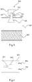
- Fig. 1 shows a waveguide coupling 100 for a level radar 200 (see. Fig. 3 ).
- the high-frequency chip 101 is arranged on a substrate 103, for example a printed circuit board 103, a ceramic carrier 103 or metal plate 103, and connected to the power supply via bonding wires 102. Control signals can also be transmitted via these bonding wires. However, the bonding wires are not used to transmit high-frequency microwave signals.
- the high-frequency chip 101 protrudes at least partially into the resonator chamber or resonant cavity 104 of the waveguide 107.
- the waveguide 107 On its underside, the waveguide 107 is completed, so that it forms a resonance space 104.
- the resonant space 104 is formed between the coupling element located on the top or bottom of the substrate 103 and the bottom, closed end of the waveguide 107.
- a horn antenna 105 is connected, via which the RF transmission signal is radiated in the direction Medgutober Design.
- a lens for signal bundling may also be provided.
- the high-frequency chip 101 extends beyond the terminal edge 108 of the substrate 103 and protrudes into the waveguide 107.
- the coupling element 401 is arranged (see. Fig. 4 ) over which the RF transmission signal is radiated. It can be provided that the transmission signal reflected on the product surface is also received via this coupling element.
- the high-frequency transmission signal (microwave signal) is coupled directly from the chip via the coupling element 401 in the waveguide.
- the elimination of RF signal transmission from the microwave chip to another medium results in improved signal transmission characteristics.
- the "ringing", which is an effect in the vicinity of the antenna, which can lead to inaccurate distance measurements in the vicinity of the antenna, is significantly reduced by the direct and simplified coupling.
- the sensitivity of the system is improved by the reduced insertion loss.
- the design technique is also simplified because the sophisticated RF signal transmission requires no connection technology.
- this arrangement has the advantage that the antenna can be placed over the waveguide 107, that is, has a distance from the substrate. For high temperature applications, this allows the electronics to be placed further away from the antenna.
- a direct coupling of the microwave signal from the chip is provided in the waveguide, wherein the coupling element itself is part of the high-frequency chip and at least partially protrudes into the waveguide.
- a coupling pin 401 is realized, as shown in the Fig. 4 is shown.
- the waveguide is placed.
- the chip is at least partially, but possibly also completely, within the waveguide.
- a coupling pin and a small patch can be used, so a flat radiator element.
- the resonator cavity 104 below the chip may be unfilled, as shown in FIG Fig. 1 is shown, or it is filled with a dielectric 106, as shown in the Fig. 2 you can see.
- the coupling pin is usually on the top of the chip part of its layouts. It can also be located on the bottom of the chip. In this case, the layout of the chip and the further structure is designed accordingly.
- the resonator cavity itself may be integrated into the substrate 103, which may be a printed circuit board or the like, as shown in FIG Fig. 2 is shown.
- the substrate 103 forms a recess (cavity) into which the waveguide 107 can be inserted.
- the RF chip itself may be glued to the substrate and electrically contacted by bonding technology to the power supply and to receive control signals.
- Alternative contacts are possible, for example by embedding the chip in a carrier material and electrical connection via a structured metallization.
- the chip is completely embedded by a material (for example plastic).
- the surface is provided with a metallization layer in which the connection lines are located. It is also possible to mount a lens for signal bundling over the entire arrangement.
- the type of feed described above can also be used to excite other types of antennas.
- the imaged bonding wires 102 serve only to supply the chip with power and other signals. They do not carry microwave signals.
- Fig. 3 shows a measurement setup with a container 301 in which contents 302 is located.
- a level gauge 300 is mounted, which has a high-frequency radar module 200 with the waveguide coupling described above.
- a dielectric lens 108 may be mounted. Additionally or alternatively to the lens 108, a gas-tight process seal 109 may be provided within the waveguide to isolate the chip from the container atmosphere.
- Fig. 4 shows a plan view of a high-frequency chip 101 with a high frequency signal generating unit 402, to which a coupling element 401 is connected.
- a high frequency signal generating unit with a coupling element in the form of a pin (line piece).
- a coupling element in the form of a pin (line piece).
- a single patch or even a patch array may be provided.
Landscapes
- Physics & Mathematics (AREA)
- Engineering & Computer Science (AREA)
- Electromagnetism (AREA)
- Radar, Positioning & Navigation (AREA)
- Remote Sensing (AREA)
- General Physics & Mathematics (AREA)
- Computer Networks & Wireless Communication (AREA)
- Thermal Sciences (AREA)
- Fluid Mechanics (AREA)
- Radar Systems Or Details Thereof (AREA)
- Waveguide Aerials (AREA)
- Variable-Direction Aerials And Aerial Arrays (AREA)
Abstract
Description
- Die Erfindung betrifft die Füllstandmessung mit Füllstandmessgeräten, die nach dem Laufzeitverfahren arbeiten. Insbesondere betrifft die Erfindung eine Hohlleitereinkopplung für ein Füllstandradar, ein Hochfrequenz-Radarmodul für ein Füllstandradar und ein Füllstandradar mit einem solchen Hochfrequenz-Radarmodul.
- Zur Messung des Füllstands eines Mediums in einem Behälter können Mikrowellensignale in die Richtung der Oberfläche ausgestrahlt und die dort reflektierten Signale vom Messgerät empfangen werden. Aus der Zeit zwischen dem Absenden der Signale und dem Empfangen der reflektierten Signale (Laufzeit) lässt sich der Abstand zwischen dem Messgerät und der Oberfläche des Mediums und daraus über bekannte Größen des Messaufbaus der Füllstand ermitteln. Daher wird das Messverfahren auch als Laufzeit- oder Radar-Verfahren bezeichnet. Die Mikrowellensignale können kontinuierlich oder pulsweise erzeugt und abgestrahlt werden.
- Derartige Füllstandmessgeräte verfügen üblicherweise über einen Hochfrequenzchip, der die Mikrowellensignale erzeugt und verarbeitet, und ein Antennenelement, das die Mikrowellensignale abstrahlt.
- Die abzustrahlenden Mikrowellensignale, im Folgenden auch als hochfrequente Sendesignale bezeichnet, werden über eine HF-Signalleitung an das Antennenelement übermittelt.
- Es ist eine Aufgabe der Erfindung, ein vorteilhaftes Füllstandradar bereitzustellen, das nach dem Laufzeitverfahren arbeitet.
- Diese Aufgabe wird durch die Gegenstände der unabhängigen Ansprüche gelöst. Weiterbildungen der Erfindung ergeben sich aus den Unteransprüchen und der nachfolgenden Beschreibung von Ausführungsformen.
- Ein erster Aspekt der Erfindung betrifft eine Hohlleitereinkopplung für ein Füllstandradar, welche einen Hohlleiter und einen Hochfrequenzchip aufweist, der zumindest teilweise in dem Hohlleiter angeordnet ist und der Erzeugung eines hochfrequenten Sendesignals dient. Der Hochfrequenzchip weist ein Koppelelement zum Einkoppeln des Sendesignals in den Hohlleiter auf.
- Bei dem Koppelelement kann es sich beispielsweise um einen Einkoppelstift in Form eines metallischen Stifts (durch Metallisierungsstruktur (z.B. Leitungsstück) handeln. Auch kann das Koppelelement in Form einer Finne oder einer Patchantenne ausgeführt sein. Der Chip mit Koppelelement sitzt zumindest teilweise im Hohlleiter.
- Bond-Verbindungen zur Verbindung des Hochfrequenzchips mit dem Koppelelement sind nicht erforderlich. Insbesondere ist es nicht erforderlich, dass das erzeugte Hochfrequenzsignal des Mikrowellenchips auf eine Leiterplatte überführt wird, bevor es dann an ein Antennenelement übertragen wird. Auch eine direkte Bondverbindung zwischen Chip und Antennenelement ist nicht erforderlich.
- Durch die Integration des Koppelelements in den Hochfrequenzchip können darüber hinaus Signalwege verkürzt werden, so dass die Länge der Zuführung vom Hochfrequenzchip zum Koppelelement eine möglichst geringe Einfügedämpfung aufweist, so dass negative Einflüsse auf die Empfindlichkeit des Radarsystems minimiert werden können.
- Da das Mikrowellensignal direkt vom HF-Chip in den Hohlleiter eingekoppelt wird (das Koppelelement ist ja Bestandteil des Hochfrequenzchips) kann auf nachteilige Signalverbindungen verzichtet werden.
- Gemäß einer Ausführungsform der Erfindung ist das Koppelelement auf der Oberseite des Hochfrequenzchips angeordnet. Gemäß einer weiteren Ausführungsform der Erfindung ist das Koppelelement auf der Unterseite des Hochfrequenzchips angeordnet.
- Beide Ausführungsformen weisen teilweise unterschiedliche Vorteile auf. Beispielsweise ist im letzteren Fall das Koppelelement mechanisch besser geschützt. Sitzt das Koppelelement auf der Oberseite des Chips, kann das Mikrowellensignal ungehindert in das darüber liegende Medium abgestrahlt werden. Es gibt keine Dämpfung durch beispielsweise das Chip-Material. Außerdem befindet sich das Koppelelement in diesem Fall auf der gleichen Chip-Seite wie der hochfrequente Schaltungsteil des Chips. Somit sind keine aufwendigen Verbindungen innerhalb des Chips zu realisieren.
- Gemäß einer weiteren Ausführungsform der Erfindung weist die Hohlleitereinkopplung ein Substrat auf, auf dem der Hochfrequenzchip angebracht ist. Das Substrat ist darüber hinaus an dem Hohlleiter befestigt, so dass sich ein sehr stabiler Aufbau ergibt.
- Gemäß einer weiteren Ausführungsform der Erfindung weist der Hohlleiter einen Resonatorraum oder Resonanzraum auf, der durch eine Ausnehmung des Substrats ausgebildet ist. Typischerweise sind die Wände des Resonatorraumes metallisiert und es kann vorgesehen sein, dass der Resonatorraum zumindest teilweise mit einem Dielektrikum gefüllt ist. Insbesondere kann vorgesehen sein, dass sich das Dielektrikum nur unterhalb des Koppelelements befindet. Auch kann das Koppelelement in dem Dielektrikum eingebettet sein.
- Gemäß einer weiteren Ausführungsform der Erfindung weist die Hohlleitereinkopplung ein Antennenhorn auf, das an das Ende des Hohlleiters angebracht ist. Der Hochfrequenzchip ist beispielsweise auf dem Substrat aufgeklebt.
- Ein weiterer Aspekt der Erfindung betrifft ein Hochfrequenz-Radarmodul für ein Füllstandradar, das eine oben und im Folgenden beschriebene Hohlleitereinkopplung aufweist.
- Ein weiterer Aspekt der Erfindung betrifft ein Füllstandradar mit dem oben und im Folgenden beschriebenen Hochfrequenz-Radarmodul.
- Im Folgenden werden mit Verweis auf die Figuren Ausführungsformen der Erfindung beschrieben. Werden in der folgenden Figurenbeschreibung die gleichen Bezugszeichen verwendet, so bezeichnen diese gleiche oder ähnliche Elemente. Die Darstellungen in den Figuren sind schematisch und nicht maßstäblich.
-
-
Fig. 1 zeigt eine Hohlleitereinkopplung gemäß einer Ausführungsform der Erfindung. -
Fig. 2 zeigt eine Hohlleitereinkopplung gemäß einer weiteren Ausführungsform der Erfindung. -
Fig. 3 zeigt ein Füllstandmesssystem gemäß einer Ausführungsform der Erfindung. -
Fig. 4 zeigt einen Hochfrequenzchip mit einem Koppelelement gemäß einer Ausführungsform der Erfindung. -
Fig. 1 zeigt eine Hohlleitereinkopplung 100 für ein Füllstandradar 200 (vgl.Fig. 3 ). Der Hochfrequenzchip 101 ist auf einem Substrat 103, beispielsweise einer Leiterplatte 103, einem Keramikträger 103 oder Metallplatte 103, angeordnet und über Bonddrähte 102 an die Energieversorgung angeschlossen. Über diese Bonddrähte können auch Steuersignale übertragen werden. Jedoch dienen die Bonddrähte nicht zur Übertragung von hochfrequenten Mikrowellensignalen. - Der Hochfrequenzchip 101 ragt zumindest teilweise in den Resonatorraum oder Resonanzraum 104 des Hohlleiters 107 hinein. An seiner Unterseite ist der Hohlleiter 107 abgeschlossen, so dass er einen Resonanzraum 104 ausbildet. Der Resonanzraum 104 ist zwischen dem Koppelelement, das sich auf der Ober- oder Unterseite des Substrats 103 befindet, und dem unteren, abgeschlossenen Ende des Hohlleiters 107 ausgebildet. Am anderen Ende des Hohlleiters ist eine Hornantenne 105 angeschlossen, über welche das HF-Sendesignal in Richtung Füllgutoberfläche abgestrahlt wird. Eine Linse zur Signalbündelung kann ebenso vorgesehen sein.
- In der Ausführungsform der
Fig. 1 befindet sich der Resonanzraum 104 des Hohlleiters 107 neben dem Substrat 103, auf dem der Hochfrequenzchip 101 angeordnet ist. Der Hochfrequenzchip 101 erstreckt sich über die Abschlusskante 108 des Substrats 103 hinaus und ragt in den Hohlleiter 107 hinein. Auf der Oberseite oder auf der Unterseite des Hochfrequenzchips ist das Koppelelement 401 angeordnet (vgl.Fig. 4 ), über welches das HF-Sendesignal abgestrahlt wird. Es kann vorgesehen sein, dass über dieses Koppelelement auch das an der Füllgutoberfläche reflektierte Sendesignal empfangen wird. - Das Hochfrequenz-Sendesignal (Mikrowellensignal) wird direkt vom Chip über das Koppelelement 401 in den Hohlleiter eingekoppelt. Der Wegfall einer HF-Signalübertragung vom Mikrowellenchip auf ein anderes Medium (beispielsweise eine Leiterplatte (PCB), abgesetzte Finne, abgesetzter Stift) resultiert in verbesserten Signalübertragungseigenschaften. Das "Klingeln", bei dem es sich um einen Effekt im Nahbereich der Antenne handelt, welcher zu ungenauen Entfernungsmessungen im Nahbereich der Antenne führen kann, wird durch die direkte und vereinfachte Einkopplung deutlich reduziert. Die Empfindlichkeit des Systems wird durch die verringerte Einfügedämpfung verbessert. Auch die Aufbautechnik wird vereinfacht, da die anspruchsvolle HF-Signalübertragung ohne Verbindungstechnik auskommt.
- Im Gegensatz zu einer Antenna-on-Chip-Lösung hat diese Anordnung den Vorteil, dass die Antenne über den Hohlleiter 107 abgesetzt werden kann, also einen Abstand zum Substrat aufweist. Bei Anwendungen mit hohen Temperaturen kann dadurch die Elektronik weiter weg von der Antenne platziert werden.
- In anderen Worten ist eine direkte Einkopplung des Mikrowellensignals vom Chip in den Hohlleiter vorgesehen, wobei das Koppelelement selbst Bestandteil des Hochfrequenz-Chips ist und zumindest teilweise in den Hohlleiter hineinragt. Auf der Chip-Fläche wird ein Einkoppelstift 401 realisiert, wie dies in der
Fig. 4 dargestellt ist. Darum herum und darüber wird der Hohlleiter angeordnet. Der Chip befindet sich zumindest teilweise, möglicherweise aber auch komplett, innerhalb des Hohlleiters. Anstelle eines Einkoppelstifts kann auch ein kleines Patch verwendet werden, also ein flächiges Strahlerelement. - Der Resonatorraum 104 unterhalb des Chips kann ungefüllt sein, wie dies in der
Fig. 1 gezeigt ist, oder er ist mit einem Dielektrikum 106 gefüllt sein, wie dies in derFig. 2 zu sehen ist. Der Koppelstift ist üblicherweise auf der Oberseite des Chips Bestandteil dessen Layouts. Er kann sich auch auf der Unterseite des Chips befinden. In diesem Fall ist das Layout des Chips und der weitere Aufbau entsprechend ausgelegt. - Der Resonatorraum selbst kann in das Substrat 103, bei dem es sich um eine Leiterplatte oder dergleichen handelt, integriert sein, wie dies in der
Fig. 2 gezeigt ist. In diesem Fall bildet das Substrat 103 eine Ausnehmung (cavity) aus, in welche der Hohlleiter 107 eingesetzt sein kann. - Der HF-Chip selbst kann auf dem Substrat aufgeklebt sein und per Bonding-Technologie elektrisch an die Energieversorgung und zur Entgegennehme von Steuerungssignalen kontaktiert sein. Alternative Kontaktierungen sind möglich, beispielsweise durch Einbetten des Chips in ein Trägermaterial und elektrischen Anschluss über eine strukturierte Metallisierungsebene. Der Chip ist dabei komplett durch ein Material (z.B. Kunststoff) eingebettet. Die Oberfläche ist mit einer Metallisierungslage versehen, in der sich die Anschlussleitungen befinden. Auch ist es möglich, eine Linse zur Signalbündelung über der gesamten Anordnung anzubringen.
- Die oben beschriebene Art der Einspeisung kann auch zur Erregung anderer Antennentypen verwendet werden.
- Die abgebildeten Bonddrähte 102 dienen nur der Versorgung des Chips mit Energie und anderen Signalen. Sie führen keine Mikrowellensignale.
-
Fig. 3 zeigt einen Messaufbau mit einem Behälter 301, in dem sich Füllgut 302 befindet. Oben an dem Behälter ist ein Füllstandmessgerät 300 angebracht, welches ein Hochfrequenzradarmodul 200 mit der oben beschriebenen Hohlleitereinkopplung aufweist. Am Ende der Hornantenne 105 kann eine dielektrische Linse 108 angebracht sein. Zusätzlich oder alternativ zur Linse 108 kann eine gasdichte Prozessabdichtung 109 innerhalb des Hohlleiters vorgesehen sein, um den Chip von der Behälteratmosphäre zu isolieren. -
Fig. 4 zeigt eine Draufsicht auf einen Hochfrequenzchip 101 mit einer Hochfrequenzsignalerzeugungseinheit 402, an die ein Koppelelement 401 angeschlossen ist. - Dargestellt ist eine Hochfrequenzsignalerzeugungseinheit mit einem Koppelelement in Form eines Stiftes (Leitungsstück). Alternativ kann ein einzelnes Patch oder auch ein Patch-Array vorgesehen sein.
- Ergänzend sei daraufhingewiesen, dass "umfassend" und "aufweisend" keine anderen Elemente oder Schritte ausschließt und die unbestimmten Artikel "eine" oder "ein" keine Vielzahl ausschließen. Ferner sei darauf hingewiesen, dass Merkmale oder Schritte, die mit Verweis auf eines der obigen Ausführungsbeispiele beschrieben worden sind, auch in Kombination mit anderen Merkmalen oder Schritten anderer oben beschriebener Ausführungsbeispiele verwendet werden können. Bezugszeichen in den Ansprüchen sind nicht als Einschränkungen anzusehen.
Claims (11)
- Hohlleitereinkopplung (100) für ein Füllstandradar (300), aufweisend:einen Hohlleiter (107);einen Hochfrequenzchip (101), der zumindest teilweise in dem Hohlleiter angeordnet ist, zur Erzeugung eines hochfrequenten Sendesignals;wobei der Hochfrequenzchip ein Koppelelement (401) zum Einkoppeln des Sendesignals in den Hohlleiter aufweist.
- Hohlleitereinkopplung nach Anspruch 1,
wobei das Koppelelement (401) als Einkoppelstift ausgeführt ist. - Hohlleitereinkopplung nach einem der vorhergehenden Ansprüche,
wobei das Koppelelement (401) auf der Oberseite des Hochfrequenzchips (101) angeordnet ist. - Hohlleitereinkopplung nach einem der Ansprüche 1 oder 2,
wobei das Koppelelement (401) auf der Unterseite des Hochfrequenzchips (101) angeordnet ist. - Hohlleitereinkopplung nach einem der vorhergehenden Ansprüche, weiter aufweisend:ein Substrat (103), auf dem der Hochfrequenzchip (101) angebracht ist;wobei das Substrat an dem Hohlleiter (107) angebracht ist.
- Hohlleitereinkopplung nach einem der vorhergehenden Ansprüche,
wobei der Hohlleiter (107) einen Resonatorraum (104) aufweist, der in eine Ausnehmung des Substrats (103) integriert ist. - Hohlleitereinkopplung nach Anspruch 6,
wobei der Resonatorraum (104) unterhalb des Hochfrequenzchips (101) mit einem Dielektrikum (106) gefüllt ist. - Hohlleitereinkopplung nach einem der vorhergehenden Ansprüche, weiter aufweisend:ein Antennenhorn (105), das an das Ende des Hohlleiters (107) angebracht ist.
- Hohlleitereinkopplung nach einem der vorhergehenden Ansprüche,
wobei der Hochfrequenzchip (101) auf dem Substrat (103) aufgeklebt ist. - Hochfrequenz-Radarmodul (200) für ein Füllstandradar, aufweisend:Hohlleitereinkopplung (100) nach einem der vorhergehenden Ansprüche.
- Füllstandradar (300) mit einem Hochfrequenz-Radarmodul (200) nach Anspruch 10.
Priority Applications (3)
| Application Number | Priority Date | Filing Date | Title |
|---|---|---|---|
| EP17188089.1A EP3450931B1 (de) | 2017-08-28 | 2017-08-28 | Hohlleitereinkopplung für ein füllstandradar |
| US16/115,065 US11099050B2 (en) | 2017-08-28 | 2018-08-28 | Waveguide coupling for a fill level radar |
| CN201810985799.2A CN109428142B (zh) | 2017-08-28 | 2018-08-28 | 波导耦合结构、高频雷达模块和填充物位雷达 |
Applications Claiming Priority (1)
| Application Number | Priority Date | Filing Date | Title |
|---|---|---|---|
| EP17188089.1A EP3450931B1 (de) | 2017-08-28 | 2017-08-28 | Hohlleitereinkopplung für ein füllstandradar |
Publications (2)
| Publication Number | Publication Date |
|---|---|
| EP3450931A1 true EP3450931A1 (de) | 2019-03-06 |
| EP3450931B1 EP3450931B1 (de) | 2022-10-05 |
Family
ID=59713922
Family Applications (1)
| Application Number | Title | Priority Date | Filing Date |
|---|---|---|---|
| EP17188089.1A Active EP3450931B1 (de) | 2017-08-28 | 2017-08-28 | Hohlleitereinkopplung für ein füllstandradar |
Country Status (3)
| Country | Link |
|---|---|
| US (1) | US11099050B2 (de) |
| EP (1) | EP3450931B1 (de) |
| CN (1) | CN109428142B (de) |
Cited By (3)
| Publication number | Priority date | Publication date | Assignee | Title |
|---|---|---|---|---|
| DE102019204671A1 (de) * | 2019-04-02 | 2020-10-08 | Vega Grieshaber Kg | Radarmodul mit Doppelfinne |
| DE102019204680A1 (de) * | 2019-04-02 | 2020-10-08 | Vega Grieshaber Kg | Radarmodul mit Mikrowellen-Chip |
| US12099137B2 (en) | 2019-04-02 | 2024-09-24 | Vega Grieshaber Kg | Radar module comprising a microwave chip |
Families Citing this family (3)
| Publication number | Priority date | Publication date | Assignee | Title |
|---|---|---|---|---|
| DE102020123754A1 (de) * | 2020-09-11 | 2022-03-17 | Endress+Hauser Conducta Gmbh+Co. Kg | Taster zur Erkennung von Phasenübergängen |
| CN112068147B (zh) * | 2020-10-15 | 2024-06-21 | 联合微电子中心有限责任公司 | 用于目标检测的集成芯片和电子装置 |
| EP4063805A1 (de) * | 2021-03-22 | 2022-09-28 | Rosemount Tank Radar AB | Mikrowellenübertragungsanordnung mit verkapselungs-, kommunikations- und/oder messsystem und radarfüllstandsmesssystem |
Citations (5)
| Publication number | Priority date | Publication date | Assignee | Title |
|---|---|---|---|---|
| EP0296838A2 (de) * | 1987-06-26 | 1988-12-28 | Texas Instruments Incorporated | Monolithischer Mikrowellen-Sender/Empfänger |
| EP0884567A1 (de) * | 1997-06-08 | 1998-12-16 | Josef Sailer | System zum Erfassen von Füllständen |
| US20040056667A1 (en) * | 2000-10-17 | 2004-03-25 | Wolfram Lutke | Level measuring instrument |
| DE102015111595A1 (de) * | 2015-07-16 | 2017-01-19 | Endress + Hauser Gmbh + Co. Kg | Füllstandmessgerät zur Ermittlung und Überwachung eines Füllstands |
| DE102015119690A1 (de) * | 2015-11-13 | 2017-05-18 | Endress + Hauser Gmbh + Co. Kg | Radarbasierter Füllstandsensor |
Family Cites Families (23)
| Publication number | Priority date | Publication date | Assignee | Title |
|---|---|---|---|---|
| US2695356A (en) * | 1948-08-14 | 1954-11-23 | Philco Corp | Image noise suppression system |
| US3462713A (en) * | 1967-07-19 | 1969-08-19 | Bell Telephone Labor Inc | Waveguide-stripline transducer |
| JPS5641001B1 (de) * | 1971-04-30 | 1981-09-25 | ||
| US3866144A (en) * | 1972-11-09 | 1975-02-11 | Yoshihiko Sawayama | Microwave oscillator |
| US4453142A (en) * | 1981-11-02 | 1984-06-05 | Motorola Inc. | Microstrip to waveguide transition |
| WO1984003008A1 (en) * | 1983-01-20 | 1984-08-02 | Matsushita Electric Ind Co Ltd | Frequency converter |
| US4716386A (en) * | 1986-06-10 | 1987-12-29 | Canadian Marconi Company | Waveguide to stripline transition |
| ATE278179T1 (de) * | 2000-05-15 | 2004-10-15 | Krohne Messtechnik Kg | Füllstandsmessgerät |
| DE10027228B4 (de) * | 2000-05-31 | 2007-05-16 | Endress & Hauser Gmbh & Co Kg | Vorrichtung zur Bestimmung und/oder Überwachung des Füllstandes eines Füllguts in einem Behälter |
| DE10064812A1 (de) * | 2000-12-22 | 2002-06-27 | Endress & Hauser Gmbh & Co Kg | Vorrichtung zum Aussenden hochfrequenter Signale |
| DE102004034251A1 (de) * | 2004-07-14 | 2006-02-09 | Vega Grieshaber Kg | Füllstands-Messvorrichtung mit einem Wellenreiter und einem Wellenanpasser |
| DE102005054233A1 (de) | 2005-11-14 | 2007-05-16 | Grieshaber Vega Kg | Hohlleiterübergang |
| EP1949491B1 (de) * | 2005-11-14 | 2011-07-06 | VEGA Grieshaber KG | Hohlleiterübergang |
| US20070133083A1 (en) * | 2005-12-07 | 2007-06-14 | Kangaslahti Pekka P | Waveguide apparatus with integrated amplifier and associated transitions |
| US8022784B2 (en) * | 2008-07-07 | 2011-09-20 | Korea Advanced Institute Of Science And Technology (Kaist) | Planar transmission line-to-waveguide transition apparatus having an embedded bent stub |
| EP2189765B1 (de) * | 2008-10-29 | 2018-04-11 | VEGA Grieshaber KG | Hochfrequenzmodul zur Füllstandmessung im W-Band |
| US9548523B2 (en) | 2014-04-09 | 2017-01-17 | Texas Instruments Incorporated | Waveguide formed with a dielectric core surrounded by conductive layers including a conformal base layer that matches the footprint of the waveguide |
| DE102014109120B4 (de) | 2014-06-30 | 2017-04-06 | Krohne Messtechnik Gmbh | Mikrowellenmodul |
| DE102014218339A1 (de) | 2014-09-12 | 2016-03-17 | Robert Bosch Gmbh | Einrichtung zur Übertragung von Millimeterwellensignalen |
| CN104362421B (zh) * | 2014-11-06 | 2017-01-25 | 电子科技大学 | 一种单基片集成的太赫兹前端 |
| US10468736B2 (en) * | 2017-02-08 | 2019-11-05 | Aptiv Technologies Limited | Radar assembly with ultra wide band waveguide to substrate integrated waveguide transition |
| DE102017203823A1 (de) | 2017-03-08 | 2018-09-13 | Vega Grieshaber Kg | Hochfrequenz-Radarmodul für ein Füllstandradar |
| DE102017203832B3 (de) | 2017-03-08 | 2018-05-03 | Vega Grieshaber Kg | Gehäuse für einen Hochfrequenzchip |
-
2017
- 2017-08-28 EP EP17188089.1A patent/EP3450931B1/de active Active
-
2018
- 2018-08-28 US US16/115,065 patent/US11099050B2/en active Active
- 2018-08-28 CN CN201810985799.2A patent/CN109428142B/zh active Active
Patent Citations (5)
| Publication number | Priority date | Publication date | Assignee | Title |
|---|---|---|---|---|
| EP0296838A2 (de) * | 1987-06-26 | 1988-12-28 | Texas Instruments Incorporated | Monolithischer Mikrowellen-Sender/Empfänger |
| EP0884567A1 (de) * | 1997-06-08 | 1998-12-16 | Josef Sailer | System zum Erfassen von Füllständen |
| US20040056667A1 (en) * | 2000-10-17 | 2004-03-25 | Wolfram Lutke | Level measuring instrument |
| DE102015111595A1 (de) * | 2015-07-16 | 2017-01-19 | Endress + Hauser Gmbh + Co. Kg | Füllstandmessgerät zur Ermittlung und Überwachung eines Füllstands |
| DE102015119690A1 (de) * | 2015-11-13 | 2017-05-18 | Endress + Hauser Gmbh + Co. Kg | Radarbasierter Füllstandsensor |
Cited By (4)
| Publication number | Priority date | Publication date | Assignee | Title |
|---|---|---|---|---|
| DE102019204671A1 (de) * | 2019-04-02 | 2020-10-08 | Vega Grieshaber Kg | Radarmodul mit Doppelfinne |
| DE102019204680A1 (de) * | 2019-04-02 | 2020-10-08 | Vega Grieshaber Kg | Radarmodul mit Mikrowellen-Chip |
| WO2020200883A1 (de) * | 2019-04-02 | 2020-10-08 | Vega Grieshaber Kg | Radarmodul mit mikrowellen-chip |
| US12099137B2 (en) | 2019-04-02 | 2024-09-24 | Vega Grieshaber Kg | Radar module comprising a microwave chip |
Also Published As
| Publication number | Publication date |
|---|---|
| CN109428142B (zh) | 2022-05-24 |
| US11099050B2 (en) | 2021-08-24 |
| US20190063983A1 (en) | 2019-02-28 |
| CN109428142A (zh) | 2019-03-05 |
| EP3450931B1 (de) | 2022-10-05 |
Similar Documents
| Publication | Publication Date | Title |
|---|---|---|
| EP3450931B1 (de) | Hohlleitereinkopplung für ein füllstandradar | |
| EP3374742B1 (de) | Radarbasierter füllstandsensor | |
| DE102009029490B4 (de) | Füllstandsmessgerät | |
| EP3361223B1 (de) | Füllstandsschalter und verfahren zur bestimmung des grenzstandes eines mediums in einem behälter | |
| DE08713469T1 (de) | Antennen für handgehaltene elektronische Vorrichtungen | |
| DE102014109120B4 (de) | Mikrowellenmodul | |
| EP3492881A1 (de) | Leiterplatte für ein radar-füllstandmessgerät mit hohlleitereinkopplung | |
| EP3894807B1 (de) | Füllstandsmessgerät | |
| EP3824258B1 (de) | Hochfrequenzbaustein | |
| EP3830894A1 (de) | Hochfrequenzbaustein | |
| DE102017112894A1 (de) | Hochfrequenz-Bauelement, insbesondere für Radar-Anwendungen | |
| DE102020133194A1 (de) | Füllstandsmessgerät | |
| EP2683022B1 (de) | Gasdichte Hohlleitereinkopplung, Hochfrequenzmodul, Füllstandradar und Verwendung | |
| EP3696516B1 (de) | Radarmodul | |
| DE102017203823A1 (de) | Hochfrequenz-Radarmodul für ein Füllstandradar | |
| DE102017203832B3 (de) | Gehäuse für einen Hochfrequenzchip | |
| WO2021099122A1 (de) | Radarchip mit einer hohlleitereinkopplung | |
| WO2021099119A1 (de) | Radarchip mit einer hohlleitereinkopplung | |
| EP3949011A1 (de) | Radarmodul mit mikrowellen-chip | |
| EP3949010A1 (de) | Radarmodul mit doppelfinne | |
| DE102019133188A1 (de) | Füllstandsmessgerät | |
| EP3699558A1 (de) | Radarsenderanordnung mit integrierter antenne | |
| EP4047742A1 (de) | Radarmodul | |
| DE10118009A1 (de) | Vorrichtung zur Bestimmung und/oder Überwachung des Füllstands eines Füllguts in einem Behälter | |
| EP2683023A1 (de) | Hohlleitereinkopplung, Hochfrequenzmodul, Füllstandradar und Verwendung |
Legal Events
| Date | Code | Title | Description |
|---|---|---|---|
| PUAI | Public reference made under article 153(3) epc to a published international application that has entered the european phase |
Free format text: ORIGINAL CODE: 0009012 |
|
| STAA | Information on the status of an ep patent application or granted ep patent |
Free format text: STATUS: REQUEST FOR EXAMINATION WAS MADE |
|
| 17P | Request for examination filed |
Effective date: 20180816 |
|
| AK | Designated contracting states |
Kind code of ref document: A1 Designated state(s): AL AT BE BG CH CY CZ DE DK EE ES FI FR GB GR HR HU IE IS IT LI LT LU LV MC MK MT NL NO PL PT RO RS SE SI SK SM TR |
|
| AX | Request for extension of the european patent |
Extension state: BA ME |
|
| STAA | Information on the status of an ep patent application or granted ep patent |
Free format text: STATUS: REQUEST FOR EXAMINATION WAS MADE |
|
| STAA | Information on the status of an ep patent application or granted ep patent |
Free format text: STATUS: EXAMINATION IS IN PROGRESS |
|
| 17Q | First examination report despatched |
Effective date: 20210628 |
|
| STAA | Information on the status of an ep patent application or granted ep patent |
Free format text: STATUS: EXAMINATION IS IN PROGRESS |
|
| RIC1 | Information provided on ipc code assigned before grant |
Ipc: H01Q 13/02 20060101ALI20220414BHEP Ipc: H01Q 1/22 20060101ALI20220414BHEP Ipc: G01S 13/88 20060101ALI20220414BHEP Ipc: G01S 7/03 20060101ALI20220414BHEP Ipc: G01F 23/284 20060101AFI20220414BHEP |
|
| INTG | Intention to grant announced |
Effective date: 20220506 |
|
| GRAS | Grant fee paid |
Free format text: ORIGINAL CODE: EPIDOSNIGR3 |
|
| STAA | Information on the status of an ep patent application or granted ep patent |
Free format text: STATUS: GRANT OF PATENT IS INTENDED |
|
| GRAA | (expected) grant |
Free format text: ORIGINAL CODE: 0009210 |
|
| STAA | Information on the status of an ep patent application or granted ep patent |
Free format text: STATUS: THE PATENT HAS BEEN GRANTED |
|
| AK | Designated contracting states |
Kind code of ref document: B1 Designated state(s): AL AT BE BG CH CY CZ DE DK EE ES FI FR GB GR HR HU IE IS IT LI LT LU LV MC MK MT NL NO PL PT RO RS SE SI SK SM TR |
|
| REG | Reference to a national code |
Ref country code: GB Ref legal event code: FG4D Free format text: NOT ENGLISH |
|
| REG | Reference to a national code |
Ref country code: CH Ref legal event code: EP |
|
| REG | Reference to a national code |
Ref country code: AT Ref legal event code: REF Ref document number: 1522993 Country of ref document: AT Kind code of ref document: T Effective date: 20221015 |
|
| REG | Reference to a national code |
Ref country code: IE Ref legal event code: FG4D Free format text: LANGUAGE OF EP DOCUMENT: GERMAN |
|
| REG | Reference to a national code |
Ref country code: DE Ref legal event code: R096 Ref document number: 502017013888 Country of ref document: DE |
|
| REG | Reference to a national code |
Ref country code: LT Ref legal event code: MG9D |
|
| REG | Reference to a national code |
Ref country code: NL Ref legal event code: MP Effective date: 20221005 |
|
| PG25 | Lapsed in a contracting state [announced via postgrant information from national office to epo] |
Ref country code: NL Free format text: LAPSE BECAUSE OF FAILURE TO SUBMIT A TRANSLATION OF THE DESCRIPTION OR TO PAY THE FEE WITHIN THE PRESCRIBED TIME-LIMIT Effective date: 20221005 |
|
| PG25 | Lapsed in a contracting state [announced via postgrant information from national office to epo] |
Ref country code: SE Free format text: LAPSE BECAUSE OF FAILURE TO SUBMIT A TRANSLATION OF THE DESCRIPTION OR TO PAY THE FEE WITHIN THE PRESCRIBED TIME-LIMIT Effective date: 20221005 Ref country code: PT Free format text: LAPSE BECAUSE OF FAILURE TO SUBMIT A TRANSLATION OF THE DESCRIPTION OR TO PAY THE FEE WITHIN THE PRESCRIBED TIME-LIMIT Effective date: 20230206 Ref country code: NO Free format text: LAPSE BECAUSE OF FAILURE TO SUBMIT A TRANSLATION OF THE DESCRIPTION OR TO PAY THE FEE WITHIN THE PRESCRIBED TIME-LIMIT Effective date: 20230105 Ref country code: LT Free format text: LAPSE BECAUSE OF FAILURE TO SUBMIT A TRANSLATION OF THE DESCRIPTION OR TO PAY THE FEE WITHIN THE PRESCRIBED TIME-LIMIT Effective date: 20221005 Ref country code: FI Free format text: LAPSE BECAUSE OF FAILURE TO SUBMIT A TRANSLATION OF THE DESCRIPTION OR TO PAY THE FEE WITHIN THE PRESCRIBED TIME-LIMIT Effective date: 20221005 Ref country code: ES Free format text: LAPSE BECAUSE OF FAILURE TO SUBMIT A TRANSLATION OF THE DESCRIPTION OR TO PAY THE FEE WITHIN THE PRESCRIBED TIME-LIMIT Effective date: 20221005 |
|
| PG25 | Lapsed in a contracting state [announced via postgrant information from national office to epo] |
Ref country code: RS Free format text: LAPSE BECAUSE OF FAILURE TO SUBMIT A TRANSLATION OF THE DESCRIPTION OR TO PAY THE FEE WITHIN THE PRESCRIBED TIME-LIMIT Effective date: 20221005 Ref country code: PL Free format text: LAPSE BECAUSE OF FAILURE TO SUBMIT A TRANSLATION OF THE DESCRIPTION OR TO PAY THE FEE WITHIN THE PRESCRIBED TIME-LIMIT Effective date: 20221005 Ref country code: LV Free format text: LAPSE BECAUSE OF FAILURE TO SUBMIT A TRANSLATION OF THE DESCRIPTION OR TO PAY THE FEE WITHIN THE PRESCRIBED TIME-LIMIT Effective date: 20221005 Ref country code: IS Free format text: LAPSE BECAUSE OF FAILURE TO SUBMIT A TRANSLATION OF THE DESCRIPTION OR TO PAY THE FEE WITHIN THE PRESCRIBED TIME-LIMIT Effective date: 20230205 Ref country code: HR Free format text: LAPSE BECAUSE OF FAILURE TO SUBMIT A TRANSLATION OF THE DESCRIPTION OR TO PAY THE FEE WITHIN THE PRESCRIBED TIME-LIMIT Effective date: 20221005 Ref country code: GR Free format text: LAPSE BECAUSE OF FAILURE TO SUBMIT A TRANSLATION OF THE DESCRIPTION OR TO PAY THE FEE WITHIN THE PRESCRIBED TIME-LIMIT Effective date: 20230106 |
|
| P01 | Opt-out of the competence of the unified patent court (upc) registered |
Effective date: 20230508 |
|
| REG | Reference to a national code |
Ref country code: DE Ref legal event code: R097 Ref document number: 502017013888 Country of ref document: DE |
|
| PG25 | Lapsed in a contracting state [announced via postgrant information from national office to epo] |
Ref country code: SM Free format text: LAPSE BECAUSE OF FAILURE TO SUBMIT A TRANSLATION OF THE DESCRIPTION OR TO PAY THE FEE WITHIN THE PRESCRIBED TIME-LIMIT Effective date: 20221005 Ref country code: RO Free format text: LAPSE BECAUSE OF FAILURE TO SUBMIT A TRANSLATION OF THE DESCRIPTION OR TO PAY THE FEE WITHIN THE PRESCRIBED TIME-LIMIT Effective date: 20221005 Ref country code: EE Free format text: LAPSE BECAUSE OF FAILURE TO SUBMIT A TRANSLATION OF THE DESCRIPTION OR TO PAY THE FEE WITHIN THE PRESCRIBED TIME-LIMIT Effective date: 20221005 Ref country code: DK Free format text: LAPSE BECAUSE OF FAILURE TO SUBMIT A TRANSLATION OF THE DESCRIPTION OR TO PAY THE FEE WITHIN THE PRESCRIBED TIME-LIMIT Effective date: 20221005 Ref country code: CZ Free format text: LAPSE BECAUSE OF FAILURE TO SUBMIT A TRANSLATION OF THE DESCRIPTION OR TO PAY THE FEE WITHIN THE PRESCRIBED TIME-LIMIT Effective date: 20221005 |
|
| PLBE | No opposition filed within time limit |
Free format text: ORIGINAL CODE: 0009261 |
|
| STAA | Information on the status of an ep patent application or granted ep patent |
Free format text: STATUS: NO OPPOSITION FILED WITHIN TIME LIMIT |
|
| PG25 | Lapsed in a contracting state [announced via postgrant information from national office to epo] |
Ref country code: SK Free format text: LAPSE BECAUSE OF FAILURE TO SUBMIT A TRANSLATION OF THE DESCRIPTION OR TO PAY THE FEE WITHIN THE PRESCRIBED TIME-LIMIT Effective date: 20221005 Ref country code: AL Free format text: LAPSE BECAUSE OF FAILURE TO SUBMIT A TRANSLATION OF THE DESCRIPTION OR TO PAY THE FEE WITHIN THE PRESCRIBED TIME-LIMIT Effective date: 20221005 |
|
| 26N | No opposition filed |
Effective date: 20230706 |
|
| PG25 | Lapsed in a contracting state [announced via postgrant information from national office to epo] |
Ref country code: SI Free format text: LAPSE BECAUSE OF FAILURE TO SUBMIT A TRANSLATION OF THE DESCRIPTION OR TO PAY THE FEE WITHIN THE PRESCRIBED TIME-LIMIT Effective date: 20221005 |
|
| PGFP | Annual fee paid to national office [announced via postgrant information from national office to epo] |
Ref country code: DE Payment date: 20230822 Year of fee payment: 7 |
|
| PG25 | Lapsed in a contracting state [announced via postgrant information from national office to epo] |
Ref country code: MC Free format text: LAPSE BECAUSE OF FAILURE TO SUBMIT A TRANSLATION OF THE DESCRIPTION OR TO PAY THE FEE WITHIN THE PRESCRIBED TIME-LIMIT Effective date: 20221005 |
|
| REG | Reference to a national code |
Ref country code: CH Ref legal event code: PL |
|
| PG25 | Lapsed in a contracting state [announced via postgrant information from national office to epo] |
Ref country code: MC Free format text: LAPSE BECAUSE OF FAILURE TO SUBMIT A TRANSLATION OF THE DESCRIPTION OR TO PAY THE FEE WITHIN THE PRESCRIBED TIME-LIMIT Effective date: 20221005 |
|
| PG25 | Lapsed in a contracting state [announced via postgrant information from national office to epo] |
Ref country code: LU Free format text: LAPSE BECAUSE OF NON-PAYMENT OF DUE FEES Effective date: 20230828 |
|
| GBPC | Gb: european patent ceased through non-payment of renewal fee |
Effective date: 20230828 |
|
| PG25 | Lapsed in a contracting state [announced via postgrant information from national office to epo] |
Ref country code: LU Free format text: LAPSE BECAUSE OF NON-PAYMENT OF DUE FEES Effective date: 20230828 Ref country code: CH Free format text: LAPSE BECAUSE OF NON-PAYMENT OF DUE FEES Effective date: 20230831 |
|
| REG | Reference to a national code |
Ref country code: BE Ref legal event code: MM Effective date: 20230831 |
|
| REG | Reference to a national code |
Ref country code: IE Ref legal event code: MM4A |
|
| PG25 | Lapsed in a contracting state [announced via postgrant information from national office to epo] |
Ref country code: IT Free format text: LAPSE BECAUSE OF FAILURE TO SUBMIT A TRANSLATION OF THE DESCRIPTION OR TO PAY THE FEE WITHIN THE PRESCRIBED TIME-LIMIT Effective date: 20221005 |
|
| PG25 | Lapsed in a contracting state [announced via postgrant information from national office to epo] |
Ref country code: IE Free format text: LAPSE BECAUSE OF NON-PAYMENT OF DUE FEES Effective date: 20230828 |
|
| PG25 | Lapsed in a contracting state [announced via postgrant information from national office to epo] |
Ref country code: GB Free format text: LAPSE BECAUSE OF NON-PAYMENT OF DUE FEES Effective date: 20230828 |
|
| PG25 | Lapsed in a contracting state [announced via postgrant information from national office to epo] |
Ref country code: IE Free format text: LAPSE BECAUSE OF NON-PAYMENT OF DUE FEES Effective date: 20230828 Ref country code: GB Free format text: LAPSE BECAUSE OF NON-PAYMENT OF DUE FEES Effective date: 20230828 Ref country code: FR Free format text: LAPSE BECAUSE OF NON-PAYMENT OF DUE FEES Effective date: 20230831 |
|
| PG25 | Lapsed in a contracting state [announced via postgrant information from national office to epo] |
Ref country code: BE Free format text: LAPSE BECAUSE OF NON-PAYMENT OF DUE FEES Effective date: 20230831 |