EP3447805A1 - Solar cell panel - Google Patents
Solar cell panel Download PDFInfo
- Publication number
- EP3447805A1 EP3447805A1 EP18189676.2A EP18189676A EP3447805A1 EP 3447805 A1 EP3447805 A1 EP 3447805A1 EP 18189676 A EP18189676 A EP 18189676A EP 3447805 A1 EP3447805 A1 EP 3447805A1
- Authority
- EP
- European Patent Office
- Prior art keywords
- solar cell
- wiring
- wirings
- electrodes
- solar
- Prior art date
- Legal status (The legal status is an assumption and is not a legal conclusion. Google has not performed a legal analysis and makes no representation as to the accuracy of the status listed.)
- Granted
Links
- 239000004065 semiconductor Substances 0.000 claims description 32
- 239000000758 substrate Substances 0.000 claims description 24
- 230000000063 preceeding effect Effects 0.000 claims 5
- 239000010410 layer Substances 0.000 description 52
- 239000000463 material Substances 0.000 description 39
- 238000007789 sealing Methods 0.000 description 18
- 238000000034 method Methods 0.000 description 14
- 230000008569 process Effects 0.000 description 14
- 238000002161 passivation Methods 0.000 description 11
- 229920005989 resin Polymers 0.000 description 9
- 239000011347 resin Substances 0.000 description 9
- 230000008602 contraction Effects 0.000 description 8
- 230000007547 defect Effects 0.000 description 8
- 230000007774 longterm Effects 0.000 description 8
- -1 polyethylene terephthalate Polymers 0.000 description 6
- 239000000853 adhesive Substances 0.000 description 5
- 230000001070 adhesive effect Effects 0.000 description 5
- 238000006243 chemical reaction Methods 0.000 description 5
- 239000004020 conductor Substances 0.000 description 5
- 230000006866 deterioration Effects 0.000 description 5
- 239000002019 doping agent Substances 0.000 description 5
- 230000000694 effects Effects 0.000 description 5
- 229920000139 polyethylene terephthalate Polymers 0.000 description 5
- 239000005020 polyethylene terephthalate Substances 0.000 description 5
- 230000009467 reduction Effects 0.000 description 5
- 230000004888 barrier function Effects 0.000 description 4
- 239000010949 copper Substances 0.000 description 4
- 229910000679 solder Inorganic materials 0.000 description 4
- 239000004593 Epoxy Substances 0.000 description 3
- 239000004698 Polyethylene Substances 0.000 description 3
- ATJFFYVFTNAWJD-UHFFFAOYSA-N Tin Chemical compound [Sn] ATJFFYVFTNAWJD-UHFFFAOYSA-N 0.000 description 3
- 239000011810 insulating material Substances 0.000 description 3
- 229910052751 metal Inorganic materials 0.000 description 3
- 239000002184 metal Substances 0.000 description 3
- 229920000573 polyethylene Polymers 0.000 description 3
- ZOXJGFHDIHLPTG-UHFFFAOYSA-N Boron Chemical compound [B] ZOXJGFHDIHLPTG-UHFFFAOYSA-N 0.000 description 2
- RYGMFSIKBFXOCR-UHFFFAOYSA-N Copper Chemical compound [Cu] RYGMFSIKBFXOCR-UHFFFAOYSA-N 0.000 description 2
- 239000002033 PVDF binder Substances 0.000 description 2
- OAICVXFJPJFONN-UHFFFAOYSA-N Phosphorus Chemical compound [P] OAICVXFJPJFONN-UHFFFAOYSA-N 0.000 description 2
- 229910052581 Si3N4 Inorganic materials 0.000 description 2
- VYPSYNLAJGMNEJ-UHFFFAOYSA-N Silicium dioxide Chemical compound O=[Si]=O VYPSYNLAJGMNEJ-UHFFFAOYSA-N 0.000 description 2
- XUIMIQQOPSSXEZ-UHFFFAOYSA-N Silicon Chemical compound [Si] XUIMIQQOPSSXEZ-UHFFFAOYSA-N 0.000 description 2
- GWEVSGVZZGPLCZ-UHFFFAOYSA-N Titan oxide Chemical compound O=[Ti]=O GWEVSGVZZGPLCZ-UHFFFAOYSA-N 0.000 description 2
- 229910045601 alloy Inorganic materials 0.000 description 2
- 239000000956 alloy Substances 0.000 description 2
- 229910052782 aluminium Inorganic materials 0.000 description 2
- XAGFODPZIPBFFR-UHFFFAOYSA-N aluminium Chemical compound [Al] XAGFODPZIPBFFR-UHFFFAOYSA-N 0.000 description 2
- 229910052796 boron Inorganic materials 0.000 description 2
- 239000000969 carrier Substances 0.000 description 2
- 239000011247 coating layer Substances 0.000 description 2
- 229910052802 copper Inorganic materials 0.000 description 2
- 239000005038 ethylene vinyl acetate Substances 0.000 description 2
- 239000010931 gold Substances 0.000 description 2
- 238000004519 manufacturing process Methods 0.000 description 2
- 229910052698 phosphorus Inorganic materials 0.000 description 2
- 239000011574 phosphorus Substances 0.000 description 2
- 229920001200 poly(ethylene-vinyl acetate) Polymers 0.000 description 2
- 229910021420 polycrystalline silicon Inorganic materials 0.000 description 2
- 229920002620 polyvinyl fluoride Polymers 0.000 description 2
- 229920002981 polyvinylidene fluoride Polymers 0.000 description 2
- 229910052710 silicon Inorganic materials 0.000 description 2
- 239000010703 silicon Substances 0.000 description 2
- HQVNEWCFYHHQES-UHFFFAOYSA-N silicon nitride Chemical compound N12[Si]34N5[Si]62N3[Si]51N64 HQVNEWCFYHHQES-UHFFFAOYSA-N 0.000 description 2
- 229910052814 silicon oxide Inorganic materials 0.000 description 2
- 238000005476 soldering Methods 0.000 description 2
- JOYRKODLDBILNP-UHFFFAOYSA-N Ethyl urethane Chemical compound CCOC(N)=O JOYRKODLDBILNP-UHFFFAOYSA-N 0.000 description 1
- GYHNNYVSQQEPJS-UHFFFAOYSA-N Gallium Chemical compound [Ga] GYHNNYVSQQEPJS-UHFFFAOYSA-N 0.000 description 1
- 239000004642 Polyimide Substances 0.000 description 1
- BQCADISMDOOEFD-UHFFFAOYSA-N Silver Chemical compound [Ag] BQCADISMDOOEFD-UHFFFAOYSA-N 0.000 description 1
- 239000012790 adhesive layer Substances 0.000 description 1
- 150000001336 alkenes Chemical class 0.000 description 1
- 229910021417 amorphous silicon Inorganic materials 0.000 description 1
- 229910052787 antimony Inorganic materials 0.000 description 1
- WATWJIUSRGPENY-UHFFFAOYSA-N antimony atom Chemical compound [Sb] WATWJIUSRGPENY-UHFFFAOYSA-N 0.000 description 1
- 229910052785 arsenic Inorganic materials 0.000 description 1
- RQNWIZPPADIBDY-UHFFFAOYSA-N arsenic atom Chemical compound [As] RQNWIZPPADIBDY-UHFFFAOYSA-N 0.000 description 1
- QVGXLLKOCUKJST-UHFFFAOYSA-N atomic oxygen Chemical compound [O] QVGXLLKOCUKJST-UHFFFAOYSA-N 0.000 description 1
- 230000008901 benefit Effects 0.000 description 1
- 229910052797 bismuth Inorganic materials 0.000 description 1
- JCXGWMGPZLAOME-UHFFFAOYSA-N bismuth atom Chemical compound [Bi] JCXGWMGPZLAOME-UHFFFAOYSA-N 0.000 description 1
- CETPSERCERDGAM-UHFFFAOYSA-N ceric oxide Chemical compound O=[Ce]=O CETPSERCERDGAM-UHFFFAOYSA-N 0.000 description 1
- 229910000422 cerium(IV) oxide Inorganic materials 0.000 description 1
- 230000008859 change Effects 0.000 description 1
- 239000003245 coal Substances 0.000 description 1
- 239000011248 coating agent Substances 0.000 description 1
- 238000000576 coating method Methods 0.000 description 1
- 229910021419 crystalline silicon Inorganic materials 0.000 description 1
- 230000002950 deficient Effects 0.000 description 1
- 230000005611 electricity Effects 0.000 description 1
- 150000002148 esters Chemical class 0.000 description 1
- 229910052733 gallium Inorganic materials 0.000 description 1
- 239000011521 glass Substances 0.000 description 1
- PCHJSUWPFVWCPO-UHFFFAOYSA-N gold Chemical compound [Au] PCHJSUWPFVWCPO-UHFFFAOYSA-N 0.000 description 1
- 229910052737 gold Inorganic materials 0.000 description 1
- 229910021478 group 5 element Inorganic materials 0.000 description 1
- 238000010438 heat treatment Methods 0.000 description 1
- 229910052739 hydrogen Inorganic materials 0.000 description 1
- 239000001257 hydrogen Substances 0.000 description 1
- 125000004435 hydrogen atom Chemical class [H]* 0.000 description 1
- 229910052738 indium Inorganic materials 0.000 description 1
- APFVFJFRJDLVQX-UHFFFAOYSA-N indium atom Chemical compound [In] APFVFJFRJDLVQX-UHFFFAOYSA-N 0.000 description 1
- 238000003475 lamination Methods 0.000 description 1
- 229910001635 magnesium fluoride Inorganic materials 0.000 description 1
- 239000007769 metal material Substances 0.000 description 1
- 229910021424 microcrystalline silicon Inorganic materials 0.000 description 1
- 238000012986 modification Methods 0.000 description 1
- 230000004048 modification Effects 0.000 description 1
- JRZJOMJEPLMPRA-UHFFFAOYSA-N olefin Natural products CCCCCCCC=C JRZJOMJEPLMPRA-UHFFFAOYSA-N 0.000 description 1
- TWNQGVIAIRXVLR-UHFFFAOYSA-N oxo(oxoalumanyloxy)alumane Chemical compound O=[Al]O[Al]=O TWNQGVIAIRXVLR-UHFFFAOYSA-N 0.000 description 1
- 229910052760 oxygen Inorganic materials 0.000 description 1
- 239000001301 oxygen Substances 0.000 description 1
- 238000012858 packaging process Methods 0.000 description 1
- 239000003208 petroleum Substances 0.000 description 1
- 229920002037 poly(vinyl butyral) polymer Polymers 0.000 description 1
- 229920001721 polyimide Polymers 0.000 description 1
- 229920001296 polysiloxane Polymers 0.000 description 1
- 239000003566 sealing material Substances 0.000 description 1
- 230000035939 shock Effects 0.000 description 1
- HBMJWWWQQXIZIP-UHFFFAOYSA-N silicon carbide Chemical compound [Si+]#[C-] HBMJWWWQQXIZIP-UHFFFAOYSA-N 0.000 description 1
- 229910010271 silicon carbide Inorganic materials 0.000 description 1
- 239000002210 silicon-based material Substances 0.000 description 1
- 229920002050 silicone resin Polymers 0.000 description 1
- 229910052709 silver Inorganic materials 0.000 description 1
- 239000004332 silver Substances 0.000 description 1
- 229910052950 sphalerite Inorganic materials 0.000 description 1
- 230000003746 surface roughness Effects 0.000 description 1
- 230000008646 thermal stress Effects 0.000 description 1
- 229910052984 zinc sulfide Inorganic materials 0.000 description 1
Images


Classifications
-
- H—ELECTRICITY
- H01—ELECTRIC ELEMENTS
- H01L—SEMICONDUCTOR DEVICES NOT COVERED BY CLASS H10
- H01L31/00—Semiconductor devices sensitive to infrared radiation, light, electromagnetic radiation of shorter wavelength or corpuscular radiation and specially adapted either for the conversion of the energy of such radiation into electrical energy or for the control of electrical energy by such radiation; Processes or apparatus specially adapted for the manufacture or treatment thereof or of parts thereof; Details thereof
- H01L31/04—Semiconductor devices sensitive to infrared radiation, light, electromagnetic radiation of shorter wavelength or corpuscular radiation and specially adapted either for the conversion of the energy of such radiation into electrical energy or for the control of electrical energy by such radiation; Processes or apparatus specially adapted for the manufacture or treatment thereof or of parts thereof; Details thereof adapted as photovoltaic [PV] conversion devices
- H01L31/042—PV modules or arrays of single PV cells
- H01L31/05—Electrical interconnection means between PV cells inside the PV module, e.g. series connection of PV cells
- H01L31/0504—Electrical interconnection means between PV cells inside the PV module, e.g. series connection of PV cells specially adapted for series or parallel connection of solar cells in a module
- H01L31/0508—Electrical interconnection means between PV cells inside the PV module, e.g. series connection of PV cells specially adapted for series or parallel connection of solar cells in a module the interconnection means having a particular shape
-
- H—ELECTRICITY
- H01—ELECTRIC ELEMENTS
- H01L—SEMICONDUCTOR DEVICES NOT COVERED BY CLASS H10
- H01L23/00—Details of semiconductor or other solid state devices
- H01L23/544—Marks applied to semiconductor devices or parts, e.g. registration marks, alignment structures, wafer maps
-
- H—ELECTRICITY
- H01—ELECTRIC ELEMENTS
- H01L—SEMICONDUCTOR DEVICES NOT COVERED BY CLASS H10
- H01L31/00—Semiconductor devices sensitive to infrared radiation, light, electromagnetic radiation of shorter wavelength or corpuscular radiation and specially adapted either for the conversion of the energy of such radiation into electrical energy or for the control of electrical energy by such radiation; Processes or apparatus specially adapted for the manufacture or treatment thereof or of parts thereof; Details thereof
- H01L31/02—Details
- H01L31/02002—Arrangements for conducting electric current to or from the device in operations
- H01L31/02005—Arrangements for conducting electric current to or from the device in operations for device characterised by at least one potential jump barrier or surface barrier
- H01L31/02008—Arrangements for conducting electric current to or from the device in operations for device characterised by at least one potential jump barrier or surface barrier for solar cells or solar cell modules
- H01L31/0201—Arrangements for conducting electric current to or from the device in operations for device characterised by at least one potential jump barrier or surface barrier for solar cells or solar cell modules comprising specially adapted module bus-bar structures
-
- H—ELECTRICITY
- H01—ELECTRIC ELEMENTS
- H01L—SEMICONDUCTOR DEVICES NOT COVERED BY CLASS H10
- H01L31/00—Semiconductor devices sensitive to infrared radiation, light, electromagnetic radiation of shorter wavelength or corpuscular radiation and specially adapted either for the conversion of the energy of such radiation into electrical energy or for the control of electrical energy by such radiation; Processes or apparatus specially adapted for the manufacture or treatment thereof or of parts thereof; Details thereof
- H01L31/02—Details
- H01L31/0224—Electrodes
- H01L31/022408—Electrodes for devices characterised by at least one potential jump barrier or surface barrier
- H01L31/022425—Electrodes for devices characterised by at least one potential jump barrier or surface barrier for solar cells
-
- H—ELECTRICITY
- H01—ELECTRIC ELEMENTS
- H01L—SEMICONDUCTOR DEVICES NOT COVERED BY CLASS H10
- H01L31/00—Semiconductor devices sensitive to infrared radiation, light, electromagnetic radiation of shorter wavelength or corpuscular radiation and specially adapted either for the conversion of the energy of such radiation into electrical energy or for the control of electrical energy by such radiation; Processes or apparatus specially adapted for the manufacture or treatment thereof or of parts thereof; Details thereof
- H01L31/04—Semiconductor devices sensitive to infrared radiation, light, electromagnetic radiation of shorter wavelength or corpuscular radiation and specially adapted either for the conversion of the energy of such radiation into electrical energy or for the control of electrical energy by such radiation; Processes or apparatus specially adapted for the manufacture or treatment thereof or of parts thereof; Details thereof adapted as photovoltaic [PV] conversion devices
- H01L31/042—PV modules or arrays of single PV cells
- H01L31/048—Encapsulation of modules
-
- H—ELECTRICITY
- H01—ELECTRIC ELEMENTS
- H01L—SEMICONDUCTOR DEVICES NOT COVERED BY CLASS H10
- H01L31/00—Semiconductor devices sensitive to infrared radiation, light, electromagnetic radiation of shorter wavelength or corpuscular radiation and specially adapted either for the conversion of the energy of such radiation into electrical energy or for the control of electrical energy by such radiation; Processes or apparatus specially adapted for the manufacture or treatment thereof or of parts thereof; Details thereof
- H01L31/04—Semiconductor devices sensitive to infrared radiation, light, electromagnetic radiation of shorter wavelength or corpuscular radiation and specially adapted either for the conversion of the energy of such radiation into electrical energy or for the control of electrical energy by such radiation; Processes or apparatus specially adapted for the manufacture or treatment thereof or of parts thereof; Details thereof adapted as photovoltaic [PV] conversion devices
- H01L31/042—PV modules or arrays of single PV cells
- H01L31/05—Electrical interconnection means between PV cells inside the PV module, e.g. series connection of PV cells
- H01L31/0504—Electrical interconnection means between PV cells inside the PV module, e.g. series connection of PV cells specially adapted for series or parallel connection of solar cells in a module
- H01L31/0516—Electrical interconnection means between PV cells inside the PV module, e.g. series connection of PV cells specially adapted for series or parallel connection of solar cells in a module specially adapted for interconnection of back-contact solar cells
-
- H—ELECTRICITY
- H01—ELECTRIC ELEMENTS
- H01L—SEMICONDUCTOR DEVICES NOT COVERED BY CLASS H10
- H01L2223/00—Details relating to semiconductor or other solid state devices covered by the group H01L23/00
- H01L2223/544—Marks applied to semiconductor devices or parts
- H01L2223/54426—Marks applied to semiconductor devices or parts for alignment
-
- Y—GENERAL TAGGING OF NEW TECHNOLOGICAL DEVELOPMENTS; GENERAL TAGGING OF CROSS-SECTIONAL TECHNOLOGIES SPANNING OVER SEVERAL SECTIONS OF THE IPC; TECHNICAL SUBJECTS COVERED BY FORMER USPC CROSS-REFERENCE ART COLLECTIONS [XRACs] AND DIGESTS
- Y02—TECHNOLOGIES OR APPLICATIONS FOR MITIGATION OR ADAPTATION AGAINST CLIMATE CHANGE
- Y02E—REDUCTION OF GREENHOUSE GAS [GHG] EMISSIONS, RELATED TO ENERGY GENERATION, TRANSMISSION OR DISTRIBUTION
- Y02E10/00—Energy generation through renewable energy sources
- Y02E10/50—Photovoltaic [PV] energy
Definitions
- Embodiments of the invention relate to a solar cell panel, and, more particularly, to a solar cell panel having an improved structure.
- a plurality of such solar cells are connected in series or in parallel by a wiring and are manufactured in a form of a solar cell panel by a packaging process for protecting the plurality of solar cells. Since a solar cell panel generates electricity for a long time in various environments, a solar cell panel is required to have long-term reliability. However, when expansion and contraction of a wiring for connecting a plurality of solar cells is repeated due to a change in temperature or the like, the wiring may be detached from a solar cell at a portion where adhesion is weak. As a result, an output of the solar cell panel is reduced, a defect rate is high, and long-term reliability may not be excellent.
- embodiments of the invention have been made in view of the above problems, and embodiments of the invention are to provide a solar cell panel having a high output, a low defect rate, and excellent long-term reliability.
- a solar cell panel includes a plurality of solar cells including a first solar cell and a second solar cell, and a wiring portion extending in a second direction crossing the first direction and electrically connecting the plurality of solar cells.
- Each of the plurality of solar cells includes a plurality of first electrodes and a plurality of second electrodes extending in a first direction.
- the wiring portion includes a first wiring connected to the plurality of first electrodes of the first solar cell, the first wiring includes a plurality of first partial wirings in the second direction in the first solar cell, and the plurality of first partial wirings are different members from each other and are electrically connected to each other by a first connection portion on the first solar cell.
- a problem caused by expansion and contraction of a wiring member can be solved by using a wiring member composed of a plurality of partial wirings having a relatively short length. Accordingly, it is possible to prevent an output reduction of a solar cell panel and deterioration or a defect of the solar cell panel and to improve long-term reliability of the solar cell panel.
- a structure of the wiring member connecting electrodes having different polarities in neighboring first and second solar cells can be simplified by differentiating an arrangement of the electrodes and connection portions in the first and second solar cells. Particularly, when electrodes having different polarities in the first and second solar cells are connected together by a common wiring, a connection structure can be simplified and an interval between the first and second solar cells can be reduced. Accordingly, efficiency of the solar cell panel can be greatly improved.
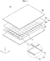
- FIG. 1 is an exploded perspective view schematically showing a solar cell panel according to an embodiment of the invention
- FIG. 2 is a cross-sectional view showing an example of a solar cell included in the solar cell panel shown in FIG. 1 .
- FIG. 2 is a cross-sectional view showing the solar cell taken along line II-II in FIG. 3 .
- a solar cell panel 100 includes a plurality of solar cells 10 and a wiring portion 20 for electrically connecting the plurality of solar cells 10.
- the solar cell panel 100 includes a sealing member 44 that surrounds and seals the solar cells 10 and the wiring portion 20, a first member 42a positioned on a front surface of the solar cells 10 on the sealing member 44, and a back member 42b positioned on a back surface of the solar cells 10 on the sealing member 44.
- the solar cell 10 may include a semiconductor substrate 110 and a first electrode 142 and a second electrode 144 disposed on one surface (e.g., a back surface) of the semiconductor substrate 110. This will be described in detail later with reference to FIG. 2 .
- the solar cell panel 100 may include a plurality of solar cells 10, and the plurality of solar cells 10 may be electrically connected in series, parallel, or series-parallel by a wiring portion 20.
- the wiring portion 20 may include a wiring member 22. At least a part of the wiring member 22 may overlap the first or second electrodes 142 or 144 of each solar cell 10 to be connected to the first or second electrodes 142 or 144. A plurality of solar cells 10 may be connected in one direction (an x-axis direction in the drawings) by the wiring member 22 to form one row (i.e., a solar cell string).
- the wiring portion 20 may further include a bus bar wiring 26 positioned at both ends of the solar cell string and connecting a solar cell string to another solar cell string or a junction box (not shown).
- the wiring member 22 or the bus bar wiring 26 may each include a conductive material (for example, a metal material).
- the wiring member 22 or the bus bar wiring 26 may include a conductive core including any one of gold (Au), silver (Ag), copper (Cu), and aluminum (Al), and a conductive coating layer that is disposed on a surface of the conductive core and includes tin (Sn) or an alloy including tin.
- the conductive core may be formed of copper (Cu), and the conductive coating layer may be formed of SnBiAg, which is an alloy including tin.
- embodiments of the invention are not limited thereto, and a material, a shape, a connection structure, etc. of the wiring member 22 or the bus bar wiring 26 may be variously modified.
- the sealing member 44 may include a first sealing member 44a positioned on front surfaces of solar cells 10 connected by the wiring portion 20 and a second sealing member 44b positioned on back surfaces of the solar cells 10 connected by the wiring portion 20.
- the first sealing member 44a and the second sealing member 44b prevent moisture and oxygen from entering and chemically bind elements of the solar cell panel 100.
- the first and second sealing members 44a and 44b may be made of an insulating material having translucency and adhesiveness.
- an ethylene-vinyl acetate copolymer resin (EVA), a polyvinyl butyral, a silicone resin, an ester-based resin, an olefin-based resin, or the like may be used for the first sealing member 44a or the second sealing member 44b.
- the back member 42b, the second sealing member 44b, the solar cells 10, the wiring portion 20, a shield member 50, and the first sealing member 44a, and the front member 42a may be integrated to constitute the solar cell panel 100 through a lamination process using the first and second sealing members 44a and 44b.
- the front member 42a is disposed on the first sealing member 44a to constitute a front surface of the solar cell panel 100 and the back member 42b is disposed on the second sealing member 44b to constitute a back surface of the solar cell panel 100.
- the front member 42a and the back member 42b may be made of an insulating material capable of protecting the solar cells 10 from external shock, moisture, ultraviolet rays, or the like.
- the front member 42a may be made of a light-transmitting material capable of transmitting light
- the back member 42b may be made of a sheet made of a light-transmitting material, a non-light-transmitting material, or a reflective material.
- the front member 42a may be formed of a glass substrate or the like, and the back member 42b may be formed of a film or a sheet.
- the back member 42b may have a TPT (Tedlar / PET / Tedlar) type or a polyvinylidene fluoride (PVDF) resin layer formed on at least one surface of a base film (for example, polyethylene terephthalate, PET).
- TPT Tedlar / PET / Tedlar
- PVDF polyvinylidene fluoride
- first or second sealing member 44a or 44b, the front member 42a, or the back member 42b may include any of various materials other than those described above, and may have any of various shapes.
- the front member 42a or the back member 42b may have any of various forms (e.g., a substrate, a film, a sheet, etc.) or any of various materials.
- FIG. 2 an example of a solar cell 10 included in the solar cell panel 100 according to the embodiment of the invention will be described in more detail.
- the solar cell 10 includes a photoelectric conversion portion including a semiconductor substrate 110, and first and second electrodes 142 and 144 connected to the photoelectric conversion portion.
- the first and second electrodes 142 and 144 may include portions formed in parallel with each other.
- the first electrode 142 and the second electrode 144 may be formed parallel to each other while being positioned together on one surface (e.g., a back surface) of the photoelectric conversion portion.
- the solar cell 10 may have a back contact structure.
- the photoelectric conversion portion may include the semiconductor substrate 110 and a conductive region 132 and 134 positioned on or at the semiconductor substrate 110.
- a first conductive region 132 and a second conductive region 134 that are involved in carriers having polarities opposite to each other may be positioned on one surface (e.g., the back surface) of the semiconductor substrate 110.
- the first and second conductive regions 132 and 134 are positioned separately from the semiconductor substrate 110 by a control passivation layer 120 interposed therebetween.
- the semiconductor substrate 110 may include a base region 112 made of a crystalline semiconductor (for example, a single-crystalline or a polycrystalline semiconductor, as an example, a single-crystalline or a polycrystalline silicon wafer, particularly, a single-crystalline silicon wafer) doped with a second conductive type dopant.
- a crystalline semiconductor for example, a single-crystalline or a polycrystalline semiconductor, as an example, a single-crystalline or a polycrystalline silicon wafer, particularly, a single-crystalline silicon wafer
- the solar cell 10 based on the semiconductor substrate 110 or the base region 112 having a high degree of crystallinity and having few defects has excellent electrical properties.
- a front surface field region 114 having the same conductivity type as the base region 112 and having a higher doping concentration than the base region 112 may be positioned on or at the front surface of the semiconductor substrate 110.
- An anti-reflection structure for example, a pyramid-shaped texturing structure including a (111) surface of the semiconductor substrate 110
- An anti-reflection structure for example, a pyramid-shaped texturing structure including a (111) surface of the semiconductor substrate 110
- the back surface of the semiconductor substrate 110 may be a mirror-polished surface or may have a smaller surface roughness than the front surface.
- embodiments of the invention are not limited thereto and various modifications are possible.
- the control passivation layer 120 may be formed of an oxide layer, a dielectric layer or an insulating layer including silicon, an oxynitride layer, an oxycarbonate layer, or the like.
- the control passivation layer 120 may be a silicon oxide layer.
- the first and second conductive regions 132 and 134 may be formed of an amorphous semiconductor, a microcrystalline semiconductor, a polycrystalline semiconductor (for example, amorphous silicon, microcrystalline silicon, or polycrystalline silicon) doped with a first or second conductive type dopant is doped.
- a carrier mobility can be high.
- a group 3 element such as boron (B), aluminum (Al), gallium (Ga), or indium (In) may be used.
- first or second conductivity type dopant is n-type
- a group 5 element such as phosphorus (P), arsenic (As), bismuth (Bi), and antimony (Sb) may be used.
- one of the first and second conductivity type dopants may be boron (B) and the other may be phosphorus (P).
- an area (for example, a width) of the first conductive region 132 may be larger than an area (for example, a width) of the second conductive region 134.
- the first conductive region 132 serving as an emitter region has a larger area than the second conductive region 134 serving as a back surface field region, which is advantageous for photoelectric conversion.
- the first and second conductive regions 132 and 134 are co-positioned in a semiconductor layer 130 to be positioned in the same plane, and a barrier region 136 formed of an intrinsic semiconductor, which is not doped, may be provided between the first and second conductive regions 132 and 134.
- control passivation layer 120 may not be provided.
- at least one of the first and second conductive regions 132 and 134 may be a doped region formed by doping a part of the semiconductor substrate 110 to constitute a part of the semiconductor substrate 110.
- the barrier region 136 may be not provided, or the barrier region 136 may include a material other than a semiconductor material or may be formed of an empty space.
- the control passivation layer 120 may not be provided.
- the first and second conductive regions 132 and 134 may be a doped region formed by doping a part of the semiconductor substrate 110 to constitute a part of the semiconductor substrate 110.
- the barrier region 136 may be not provided, or the barrier region 136 may include a material other than a semiconductor material or may be formed of an empty space.
- Various other variations are possible.
- a front passivation layer 124 and/or an anti-reflection layer 126 is entirely formed on the front surface of the semiconductor substrate 110 (more particularly, on the front surface field region 114 formed on or at the front surface of the semiconductor substrate 110).
- a back passivation layer 140 may be entirely positioned on the back surface of the semiconductor layer 130 except for a contact hole 140a.
- the front passivation layer 124, the anti-reflection layer 126, or the back passivation layer 140 may include one layer of a silicon nitride layer, a silicon nitride layer including hydrogen, a silicon oxide layer, a silicon oxynitride layer, an aluminum oxide layer, a silicon carbide layer, MgF 2 , ZnS, TiO 2 , and CeO 2 , or a multi-layered structure which two or more layers including at least one of the above are stacked.
- the first electrode 142 is electrically connected to (e.g., in contact with) the first conductive region 132 through the contact hole 140a and the second electrode 144 is electrically connected to (e.g., in contact with) the second conductive region 134 through the contact hole 140a.
- the first electrode 142 and the second electrode 144 may be formed of a conductive material (e.g., a metal).
- the solar cell 10 may further include a pad electrode 224a and 224b (refer to FIG. 3 ), which will be described later in more detail with reference to FIGS. 3 and 4 .
- the solar cell 10 is electrically connected to another solar cell 10 by the wiring portion 20 including the wiring member 22.
- the wiring portion 20 including the wiring member 22.
- FIG. 3 is a back plan view schematically showing two solar cells 10, a wiring member 22, an insulating member 34, and a connecting member 32 included in the solar cell panel 100 shown in FIG. 1 .
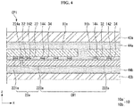
- FIG. 4 is a cross-sectional view showing the solar cell panel 100 taken along line IV-IV of FIG. 3 .
- Two solar cells 10 adjacent to each other are referred to as a first solar cell 10a and a second solar cell 10b in the following description for clear distinction.
- a first electrode 142 of a first solar cell 10a and a second electrode 144 of a second solar cell 10b are electrically connected by a plurality of wiring members 22.
- the first electrode 142 may include a plurality of first electrodes 142 longitudinally extending in a first direction (a y-axis direction in the drawings), and the second electrode 144 may include a plurality of second electrodes 144 longitudinally extending in the first direction.
- the first electrodes 142 and the second electrodes 144 may be alternately disposed in a second direction (an x-axis direction in the drawings) crossing the first direction.
- the first and second conductive regions 132 and 134 may have shapes corresponding to the first and second electrodes 142 and 144, respectively. Accordingly, the first conductive region 132 may include a plurality of portions extending in the first direction to correspond to the plurality of first electrodes 142. The second conductive region 134 may include a plurality of portions extending in the first direction to correspond to the plurality of second electrodes 144. However, the first and second conductive regions 132 and 134 may have a greater width than the first and second electrodes 142 and 144, respectively.
- a barrier region 136 may be positioned between the first conductive region 132 and the second conductive region 134. However, embodiments of the invention are not limited thereto, and the first and second conductive regions 132 and 134 may have different shapes from the first and second electrodes 142 and 144.
- the wiring member 22 in each of the first and second solar cells 10a and 10b may include a first wiring 22a connected to one of the first and second electrodes 142 and 144 and a second wiring 22b connected to the other of the second electrodes 142 and 144.
- first wirings 22a the wiring members 22 positioned at one same position (for example, a first position PI) in the first direction in the first and second solar cells 10a and 10b are referred to as first wirings 22a, and the wiring members 22 positioned at another same position different from the first position PI in the first direction (for example, the second position P2) are referred to as second wirings 22b.
- any one of the first and second wirings 22a and 22b is electrically connected to the first electrode 142 through the connecting member 32 and is insulated from the second electrode 144 through the insulating member 34, and the other one of the first and second wirings 22a and 22b is electrically connected to the second electrode 144 through the connecting member 32 and is insulated from the first electrode 142 through the insulating member 34.
- the plurality of first wirings 22a and the plurality of second wirings 22b are provided in the solar cell 10, and the first wirings 22a and the second wirings 22b are alternately positioned in the first direction. Then, the plurality of first and second wirings 22a and 22b are connected to the first and second electrodes 142 and 144 with a uniform interval, and the carriers can be effectively transferred.
- the connecting member 32 may include any of various conductive materials, and the insulating member 34 may include any of various insulating materials.
- the connecting member 32 may be formed of a material included in the first and second electrodes 142 and 144 and/or the wiring member 22, or a mixed material including the material included in the first and second electrodes 142 and 144 and/or the wiring member 22.
- the connecting member 32 may include the material included in the first and second electrodes 142 and 144 and/or the wiring member 22 by a process where the wiring member 22 is placed on the first and second electrodes 142 and 144 and is heated or so on.
- the connecting member 32 may include a solder paste layer, an epoxy solder paste layer, or the like.
- the connecting member 32 may include a low-temperature solder paste layer and a high-temperature solder paste layer together.
- the insulating member 34 may include any of a silicone-based resin, an epoxy-based resin, a urethane-based resin, an acryl-based resin, polyimide, polyethylene, and the like.
- the first wiring 22a may extend in the second direction to overlap the plurality of first electrodes 142 to be connected to the plurality of first electrodes 142 in the first solar cell 10a.
- the second wiring 22b may extend in the second direction to overlap the plurality of second electrodes 144 to be connected to the plurality of second electrodes 144 in the first solar cell 10a.
- the first wiring 22a extends to one side (a right side in FIG. 3 and 4 ) of the first solar cell 10a in the second direction and is electrically connected to the second solar cell 10b positioned at the one side (the right side in FIG.
- the second wiring 22b extends to the other side (a left side in FIGS. 3 and 4 ) of the first solar cell 10a and is electrically connected to a solar cell 10 (that is, a third solar cell) positioned at the other side (the left side in FIGS. 3 and 4 ) of the first solar cell 10a.
- the connecting members 32 may be positioned between the first wiring 22a and the plurality of first electrodes 142 at portions where the first wiring 22a and the plurality of first electrodes 142 overlap each other, and the insulating members 34 may be positioned between the first wiring 22a and the plurality of second electrodes 144 at portions where the first wiring 22a and the plurality of second electrodes 144 overlap each other.
- the connecting members 32 may be positioned between the second wiring 22b and the plurality of second electrodes 144 at portions where the second wiring 22b and the plurality of second electrodes 144 overlap each other, and the insulating members 34 may be positioned between the second wiring 22b and the plurality of first electrodes 142 at portions where the second wiring 22b and the plurality of first electrodes 142 overlap each other.
- the first wiring 22a may include a plurality of first partial wirings 221a and 222a in the second direction in the first solar cell.
- the first partial wirings 221a and 222a are different members having separate structures from each other and are electrically connected to each other by a first connection portion CP1 on the first solar cell 10a.
- the plurality of first partial wirings 221a and 222a included in the first wiring 22a may be positioned at the same position in the first direction and extend in the second direction.
- the wiring member 22 may be separated from the solar cell 10 or the wiring member 22 may be damaged or torn by the expansion and contraction of the wiring member 22.
- Such a problem may become more serious as the length of the wiring member 22 becomes larger. If such a problem occurs, the solar cell panel 100 may be judged as defective and an output of the solar cell panel 100 may be lowered.
- the problem caused by the expansion and contraction of the wiring member 22 may be more serious.
- the problem caused by the expansion and contraction of the wiring member 22 can be prevented by using the first wiring 22a composed of the plurality of first partial wirings 221a and 222a having a relatively short length. Accordingly, it is possible to prevent an output reduction of the solar cell panel 100 and deterioration or a defect of the solar cell panel 100 and to improve long-term reliability of the solar cell panel 100.
- the plurality of first partial wirings 221a and 222a may include at least one first internal wiring 221a positioned only in the first solar cell 10a and at least one first extended wiring 222a electrically connected to the first internal wiring 221a and extending from a side adjacent to the first internal wiring 221a to an outside of one side (a right side in FIGS. 3 and 4 ) of the first solar cell 10a.
- one first internal wiring 221a is provided and one first extended wiring 222a is provided, and one first connection portion CP1 where the first internal wiring 221a and the first extended wiring 222a are connected is provided in the first solar cell 10a.
- a number of the plurality of first partial wirings 221a and 222a can be minimized, and a process of attaching the first wirings 22a can be simplified.
- embodiments of the invention are not limited thereto.
- At least two first internal wirings 221a may be provided in the first solar cell 10a.
- a number of the first connection portions CP1 may be equal to a number of the first internal wirings 221a.
- lengths of the first internal wirings 221a and intervals of the first connection portions CP1 may be uniform or may be different from each other.
- the first connection portion CP1 may be positioned at a central portion of the first solar cell 10a in the second direction. Then, the first internal wiring 221a and the first extended wiring 222a are symmetrically positioned in the first solar cell 10a, and a problem caused by thermal stress can be minimized. However, embodiments of the invention are not limited to this, and the first connection portion CP1 may be positioned at a part other than the central portion of the first solar cell 10a.
- each of a plurality of first wirings 22a includes a plurality of first partial wirings 221a and 222a. According to this, effect by the plurality of first partial wirings 221a and 222a can be maximized.
- embodiments of the invention are not limited to this, and at least one of the plurality of first wirings 22a may include a plurality of first partial wirings 221a and 222a.
- the first connection portions CP1 of the plurality of first wirings 22a are positioned at the same position in the first direction.
- embodiments of the invention are not limited thereto, and at least two first wires 22a having the first connection portions CP1 at different positions may be provided.
- the first connection portion CP1 may be a first pad electrode 224a formed on the first solar cell 10a. That is, the plurality of first partial wirings 221a and 222a are electrically connected to the first pad electrode 224a, respectively, so that the plurality of first partial wirings 221a and 222a can be electrically connected to each other.
- FIGS. 3 and 4 it is exemplified that a part of each of the plurality of first partial wirings 221a and 222a is overlapped with the first pad electrode 224a. In this instance, as shown in FIG.
- connection members 32 may be positioned between the plurality of first partial wirings 221a and 222a and the first pad electrodes 224a so that the plurality of first partial wirings 221a and 222a and the first pad electrodes 224a are electrically and physically connected to each other.
- first partial wirings 221a and 222a and/or the first pad electrodes 224a may be melted using a soldering process without the connecting members 32, thereby connecting the first partial wirings 221a and 222a and the first pad electrodes 224a.
- Various other variations are possible.
- the first pad electrode 224a is positioned on an insulating layer (that is, the back passivation layer 140).
- the first pad electrode 224a may be a floating electrode being spaced apart from the semiconductor substrate 110 and the first and second conductive regions 132 and 134 and the first pad electrode 224a may be involved only in the connection between the plurality of first partial wirings 221a and 222a.
- problems such as unwanted shunts and the like can be effectively prevented without modifying a design of the first and second conductive regions 132 and 134.
- embodiments of the invention are not limited thereto.
- the first pad electrode 224a may be connected to the first conductive region 132 through the insulating layer. Then, the first pad electrode 224a may be formed together with the first electrode 142 to simplify a process. Alternatively, the first pad electrode 224a may be an electrode extended from the first electrode 142.
- Various other variations are possible.
- the first pad electrode 224a may be formed of any of various materials having conductivity (e.g., a metal).
- the first pad electrode 224a may be formed of the same material as the first and/or second electrodes 142 and/or 144, or may be formed of different materials from the first and/or second electrodes 142 and/or 144.
- a width of the first pad electrode 224a in the first direction is larger than a width of the first wiring 22a (that is, widths of the plurality of first partial wirings 221a and 222a) in the first direction for stable connection.
- the plurality of first partial wirings 221a and 222a may be spaced apart from each other on the first pad electrode 224a to minimize the length of the plurality of first partial wirings 221a and 222a.
- embodiments of the invention are not limited thereto.
- the width of the first pad electrode 224a in the first direction may be equal to or smaller than the width of the first wiring 22a (that is, the widths of the plurality of first partial wirings 221a and 222a) in the first direction.
- the plurality of first partial wirings 221a and 222a may be connected to each other or may overlap each other on the first pad electrode 224a.
- Various other variations are possible.
- the second wiring 22b may include a plurality of second partial wirings 221b and 222b in the second direction in the second solar cell.
- the second partial wirings 221b and 222b are different members having separate structures from each other and are electrically connected to each other by a second connection portion CP2 on the first solar cell 10a.
- the plurality of second partial wirings 221b and 222b included in the second wiring 22b may be positioned at the same position in the first direction and extend in the second direction.
- the plurality of second partial wirings 221b and 222b may include at least one second internal wiring 221b positioned only in the first solar cell 10a and at least one second extended wiring 222b electrically connected to the second internal wiring 221b and extending from a side adjacent to the second internal wiring 221b to an outside of the other side (a left side in FIGS. 3 and 4 ) of the first solar cell 10a.
- one second internal wiring 221b is provided and one second extended wiring 222b is provided, and one second connection portion CP2 where the second internal wiring 221b and the second extended wiring 222b are connected is provided in the first solar cell 10a.
- At least two second internal wirings 221b may be provided in the first solar cell 10a.
- a number of the second connection portions CP2 may be equal to a number of the second internal wirings 221b.
- lengths of the second internal wirings 221b and intervals of the second connection portions CP2 may be uniform or may be different from each other.
- the second connection portion CP2 may be positioned at a central portion of the first solar cell 10a in the second direction.
- embodiments of the invention are not limited to this, and the second connection portion CP2 may be positioned at a part other than the central portion of the first solar cell 10a.
- each of a plurality of second wirings 22b includes a plurality of second partial wirings 221b and 222b. According to this, effect by the plurality of second partial wirings 221b and 222b can be maximized.
- embodiments of the invention are not limited to this, and at least one of the plurality of second wirings 22b may include a plurality of second partial wirings 221b and 222b.
- the second connection portions CP2 of the plurality of second wirings 22b are positioned at the same position in the second direction.
- embodiments of the invention are not limited thereto, and at least two second wires 22b having the second connection portions CP2 at different positions may be provided.
- the second connection portion CP2 may be a second pad electrode 224b formed on the first solar cell 10a. That is, the plurality of second partial wirings 221b and 222b are electrically connected to the second pad electrode 224b, respectively, so that the plurality of second partial wirings 221b and 222b can be electrically connected to each other.
- FIGS. 3 and 4 it is exemplified that a part of each of the plurality of second partial wirings 221b and 222b is overlapped with the second pad electrode 224b.
- the connection members 32 may be positioned between the plurality of second partial wirings 221b and 222b and the second pad electrodes 224b.
- the second partial wirings 221b and 222b and/or the second pad electrodes 224b may be melted using a soldering process without the connecting members 32, thereby connecting the second partial wirings 221b and 222b and the second pad electrodes 224b.
- soldering process without the connecting members 32, thereby connecting the second partial wirings 221b and 222b and the second pad electrodes 224b.
- Various other variations are possible.
- the second pad electrode 224b is positioned on an insulating layer (that is, the rear passivation layer 140).
- the second pad electrode 224b may be a floating electrode being spaced apart from the semiconductor substrate 110 and the second and second conductive regions 132 and 134 and the second pad electrode 224b may be involved only in the connection between the plurality of second partial wirings 221b and 222b.
- embodiments of the invention are not limited thereto.
- the second pad electrode 224b may be connected to the second conductive region 132 through the insulating layer. Then, the second pad electrode 224b may be formed together with the second electrode 142 to simplify a process.
- the second pad electrode 224b may be formed of any of various materials having conductivity (e.g., a metal).
- the second pad electrode 224b may be formed of the same material as the first and/or second electrodes 142 and/or 144, or may be formed of different materials from the first and/or second electrodes 142 and/or 144.
- a width of the second pad electrode 224b in the first direction is larger than a width of the second wiring 22b (that is, widths of the plurality of second partial wirings 221b and 222b) in the first direction for stable connection.
- the plurality of second partial wirings 221b and 222b may be spaced apart from each other on the second pad electrode 224b to minimize the length of the plurality of second partial wirings 221b and 222b.
- embodiments of the invention are not limited thereto.
- the width of the second pad electrode 224b in the first direction may be equal to or smaller than the width of the second wiring 22b (that is, the widths of the plurality of second partial wirings 221b and 222b) in the first direction.
- the plurality of second partial wirings 221b and 222b may be connected to each other or may overlap each other on the second pad electrode 224b.
- Various other variations are possible.
- the first wirings 22a and the second wirings 22b may be alternately arranged in the first direction. More specifically, in a portion adjacent to the one side (e.g., the right side in FIG. 3 ) of the first solar cell 10a, the first extended wirings 222a and the second internal wirings 221b may be alternatively positioned in the first direction. In the other portion, the first internal wirings 221a and the second extended wirings 222b may alternately be positioned in the first direction. As a result, the second solar cell 10b and the third solar cell positioned on both sides of the first solar cell 10a in the second direction can be electrically connected in series to the first solar cell 10. In FIG. 3 , the first pad electrode 424a and the second pad electrode 424b are positioned at the same positions when viewed in the second direction, but embodiments of the invention are not limited thereto.
- a connection structure of the first and second wirings 22a and 22b, the first and second electrodes 142 and 144, and the first and second connection portions CP1 and CP2 in the second solar cell 10b positioned adjacent to the one side of the first solar cell 10a may be different from that in the first solar cell 10a.
- the above description of the first and second wirings 22a and 22b, the first and second electrodes 142 and 144 and the first and second connection portions CP1 and CP2 in the first solar cell 10a may be applied as it is to the first and second wirings 22a and 22b, the first and second electrodes 142 and 144 and the first and second connection portions CP1 and CP2 in the second solar cell 10b, except for the connection structure.
- the first wiring 22a is electrically connected to the second electrode 144, and the second wiring 22b is electrically connected to the first electrode 142.
- the first internal wiring 221a is positioned on the one side (the right side in FIGS. 3 and 4 ) of the second solar cell 10b, and the first extended wiring 222a extends to the other side (the left side in FIGS. 3 and 4 ) of the second solar cell 10b.
- the second internal wiring 221b is positioned on the other side of the second solar cell 10b and the second extended wiring 222b extends to the one side of the second solar cell 10b. Accordingly, in a portion adjacent to the one side (e.g., the right side in FIG. 3 ) of the second solar cell 10b, the first internal wirings 221a and the second extended wirings 222b may be alternatively positioned in the first direction. In the other portion, the first extended wirings 222a and the second internal wirings 221b may alternately be positioned in the first direction.
- first wirings 22a and the second wirings 22b are alternatively positioned in the first direction in the second solar cell 10b; however, it is contrary to an arrangement in the first solar cell 10a. That is, when viewed in the first direction, an order of the first connection portion CP1 and the second connection portion CP2 is repeated in the first solar cell 10a, while an order of the second connection portion CP2 and the first connection portion CP1 is repeated in the second solar cell 10b.
- the first electrode 142 of the first solar cell 10a and the second electrode 144 of the second solar cell 10b are electrically connected to each other by connecting the first wiring 22a of the first solar cell 10a and the first wiring 22a of the second solar cell 10b.
- the second electrode 144 of the first solar cell 10a and the first electrode 142 of another solar cell 10 that is, a third solar cell 10.
- first solar cell 10a are electrically connected to each other by connecting the second wiring 22b of the first solar cell 10a and the second wiring 22b of the third solar cell 10.
- first electrode 142 of the second solar cell 10b and the second electrode 144 of other solar cell 10 that is, a fourth solar cell 10) positioned on the one side (the right side of FIG. 3 ) of the second solar cell 10b are electrically connected to each other by connecting the second wiring 22b of the first solar cell 10a and the second wiring 22b of the fourth solar cell 10.
- the plurality of solar cells 10 can be electrically connected with each other by connecting the first wirings 22a positioned at the same first position PI in the first direction in the two neighboring solar cells 10 with each other and connecting the second wirings 22b positioned at the same second position P2 in the first direction in the two neighboring solar cells 10 with each other.
- the plurality of solar cells 10 can be electrically connected with each other by an easy and simple structure.
- the first extended wiring 222a of the first solar cell 10a and the first extended wiring 222a of the second solar cell 10b which are positioned at the same position in the first direction, are formed of a single first common wiring CW1 having a single body having an elongated structure.
- the first common wiring CW1 extends from the first connection portion CP1 of the first solar cell 10a to the second connection portion CP2 of the second solar cell 10b through a space between the first solar cell 10a and the second solar cell 10b.
- the first common wiring CW1 is connected to the first electrode 142 in the first solar cell 10a and is connected to the second electrode 144 in the second solar cell 10b. Then, a total number of the first wirings 22a formed of the plurality of first partial wirings 221a and 222a in the first and second solar cells 10a and 10b can be reduced, and thus, an attaching process of the wiring portion 20 can be simplified.
- the second extended wiring 222b of the first solar cell 10a and the second extended wiring 222b of the third solar cell 10 that is positioned at the other side (the left side of FIG. 3 ), which are positioned at the same position in the first direction, are formed of a single second common wiring CW2 having a single body having an elongated structure.
- the second common wiring CW2 extends from the second connection portion CP2 of the first solar cell 10a to the second connection portion CP2 of the third solar cell 10 through a space between the first solar cell 10a and the third solar cell 10.
- the second common wiring CW2 is connected to the second electrode 144 in the first solar cell 10a and is connected to the first electrode 142 in the third solar cell 10.
- the second extended wiring 222b of the second solar cell 10b and the second extended wiring 222b of the fourth solar cell 10 that is positioned at the one side (the right side of FIG. 3 ), which are positioned at the same position in the first direction, are formed of a single second common wiring CW2 having a single body having an elongated structure.
- the second common wiring CW2 extends from the first connection portion CP1 of the second solar cell 10b to the second connection portion CP2 of the fourth solar cell 10 through a space between the second solar cell 10b and the fourth solar cell 10.
- the second common wiring CW2 is connected to the first electrode 142 in the second solar cell 10b and is connected to the second electrode 144 in the fourth solar cell 10.
- an additional or separate wiring or structure for connecting the first wiring of the first solar cell 10a and the second wiring of the second solar cell 10b is required.
- an additional wiring which is formed in a direction crossing the first and second wirings 22a and 22b (for example, a connection wiring 24 shown in FIG. 10 ) between the first solar cell 10a and the second solar cell 10b, or the like are required.
- the above-described additional or separate wiring or the structure or the additional wiring formed in the direction crossing the first and second wirings 22a and 22b can be removed, and an attaching process of the wiring portion 20, a material cost, and the like can be reduced.
- an interval between the first solar cell 10a and the second solar cell 10b can be reduced, and efficiency of the solar cell panel 100 can be improved.
- end portions of the plurality of first partial wirings 221a and 222a and the plurality of second partial wirings 221b and 222b are spaced apart from an edge of the solar cell 10 (for example, at a central portion).
- the end portions of the plurality of first partial wirings 221a and 222a and the plurality of second partial wirings 221b and 222b are fixed by the connecting members 32 closely or densely positioned, and therefore, fixing stability of the plurality of first partial wirings 221a and 222a and the plurality of second partial wirings 221b and 222b can be enhanced.
- first solar cell 10a is used as the first solar cell 10a as it is, and the other neighboring solar cell 10 is rotated 180 degrees and is used as the second solar cell 10b. That is, the first solar cell 10a and the second solar cell 10b may be symmetric in origin.
- Such a pair of first and second solar cells 10a and 10b are repeatedly positioned so that a solar cell string composed of a plurality of solar cells 10 can be formed.
- alignment marks 50a or 50b having the same shape may be positioned at different positions in the first solar cell 10a and the second solar cell 10b.
- a first alignment mark 50a is positioned at an upper left side of FIG. 3 and a second alignment mark 50b is positioned at a lower right side of FIG. 3 in the first solar cell 10a
- a first alignment mark 50a is positioned at a lower right side of FIG. 3
- a second alignment mark 50b is positioned at an upper left side of FIG. 3 in the second solar cell 10b.
- one of the first and second solar cells 10a and 10b is positioned as it is and the other is rotated 180 degrees by the alignment marks 50a and 50b.
- the plurality of solar cells 10 can be manufactured by the same process, and the first or second common wiring CW1 or CW2 can be applied, thereby simplifying a manufacturing process.
- a problem caused by expansion and contraction of the wiring member 22 can be solved by using the wiring member 22 composed of the plurality of partial wirings 221a and 222a (221b and 222b) having a relatively short length. Accordingly, it is possible to prevent an output reduction of the solar cell panel 100 and deterioration or a defect of the solar cell panel 100 and to improve long-term reliability of the solar cell panel 100. Also, a structure of the wiring member 22 connecting the electrodes 142 and 144 having different polarities in the first and second solar cells 10a and 10b can be simplified by differentiating an arrangement of the electrodes 142 and 144 and the connection portions CP1 and CP2 in the first and second solar cells 10a and 10b.
- the connection structure can be simplified and an interval between the first and second solar cells 10a and 10b can be reduced. Accordingly, efficiency of the solar cell panel 100 can be greatly improved.
- first wiring 22a has the plurality of first partial wirings 221a and 222a and the second wiring 22b has the plurality of second partial wirings 221b and 222b in the above
- one of the first and second wirings 22a and 22b may have a plurality of wiring portions 221a and 222a or 221b and 222b.
- FIG. 5 is a back plan view schematically showing a solar cell panel according to another embodiment of the invention. For reference, a portion corresponding to the enlarged portion of FIG. 3 is shown in FIG. 5 .
- an auxiliary connecting member 32a is positioned at a portion spaced apart from a first pad electrode 224a and adjacent to an end portion of a first internal wiring 221a adjacent to the first pad electrode 224a. Thereby, an adhesion force of the first internal wiring 221a can be further improved.
- the auxiliary connecting member 32a is a connecting member positioned on an insulating layer (that is, a back passivation layer 140) at a portion where first and second electrodes 142 and 144 are not formed.
- the auxiliary connecting member 32a may be made of the same material as a connecting member 32 or may be made of a different material from the connecting member 32.
- an end portion of the first extended wiring 222a adjacent to the first pad electrode 224a is connected and fixed by the connecting member 32 on the first electrode 142 at a portion spaced apart from the first pad electrode 224a and adjacent to the end portion of the first extended wiring 222a.
- an adhesion force of the first extended wiring 222a can be further improved.
- an auxiliary connecting member 32a for the first extended wiring 222a is not formed by using the connecting member 32 positioned on the first electrode 142 as it is, it is possible to reduce a material cost and simplify a process.
- an auxiliary connecting member 32a may be further positioned at the end portion of the first extended wiring 222a.
- the connecting member 32 may be positioned at the end portion of the first internal wiring 221a and the auxiliary connecting member 32a may be positioned at the end portion of the first extended wiring 222a.
- Various other variations are possible.
- the connecting member 32 or the auxiliary connecting member 32a is positioned at the portion spaced apart from the first pad electrode 224a and adjacent to the end portions of the first partial wirings 221a and 222a adjacent to the first pad electrode 224a.
- the adhesion force of the plurality of first partial wirings 221a and 222a can be improved.
- a connecting member 32 or an auxiliary connecting member 32a is positioned at each of portions spaced apart from a second pad electrode 224b and adjacent to end portions of a plurality of second partial wirings 221b and 222b adjacent to the second pad electrode 224b. An adhesion force of the second partial wirings 221b and 222b can be improved.
- the positions of the first pad electrode 224a and the second pad electrode 224b in a second direction are different from each other and thus at least one end portions of the plurality of first partial wirings 221a and 222a and at least one end portions of the plurality of second partial wirings 221b and 222b are connected by the connecting member 32 to minimize a number of auxiliary connecting members 32a.
- embodiments of the invention are not limited thereto.
- FIG. 6 is a partial cross-sectional view showing a solar cell panel according to yet another embodiment of the invention. For reference, a portion corresponding to FIG. 4 is shown in FIG. 6 .
- a plurality of first partial wirings 221a and 222a constituting a first wiring 22a include a first overlapping portion 226a where the plurality of first partial wirings 221a and 222a overlap each other at a first connection portion CP1 to be electrically connected each other.
- the plurality of first partial wirings 221a and 222a may be electrically and physically connected to each other in the first overlapping portion 226a to form the first connection portion CP1.
- a plurality of second partial wirings constituting a second wiring may overlap each other (for example, in contact with each other) and electrically connected to each other at a second overlapping portion for constituting a second connection portion.
- a separate adhesive layer, an adhesive material, or the like for adhering the first partial wirings 221a and 222a or the plurality of second partial wirings between the first partial wirings 221a and 222a or the plurality of second partial wirings in the first overlapping portion 226a or the second overlapping portion may be further provided.
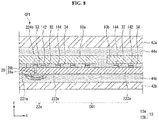
- FIG. 7 is a back plan view schematically showing two solar cells, a wiring member, an insulating member, and a connecting member included in a solar cell panel according to still another embodiment of the invention
- FIG. 8 is a cross-sectional view showing the solar cell panel taken along line VIII-VIII of FIG. 7 .
- a fixing member 28 for fixing a plurality of first partial wirings 221a and 222a at a first connection portion CP1 and/or for fixing a plurality of second partial wirings 221b and 222b at a second connection portion CP2 may be further included.
- the plurality of first and/or second partial wirings 221a and 222a and/or 221b and 222b can be stably fixed.
- the fixing member 28 may be formed to entirely cover portions of the plurality of first partial wirings 221a and 222a positioned at the first connection CP1. That is, the fixing member 28 can fix or attach at least the plurality of first partial wirings 221a and 222a to the solar cell 10.
- fixing stability of the plurality of first and/or second partial wirings 221a and 222a and/or 221b and 222b and strength of the plurality of first and/or second partial wirings 221a and 222a and/or 221b and 222b can be enhanced by the fixing member 28.
- the first and/or second partial wirings 221a and 222a and/or 221b and 222b are surrounded by the fixing member 28 so that the sealing member 44 is spaced from the first and second connection portions CP1 and CP2 with the fixing member 28 therebetween at a surface where the fixing member 28 is positioned. Then, the sealing material 44 cannot penetrate between the solar cell 10 and the plurality of first or second partial wirings 221a and 222a or 221b and 222b at the first or second connection portion CP1 or CP2, and therefore, the fixing stability of the first and second wirings 22a and 22b can be further improved. Accordingly, it is possible to prevent an output reduction of a solar cell panel 100 and deterioration or a defect of the solar cell panel 100 and to improve long-term reliability of the solar cell panel 100.
- a width of the fixing member 28 in the second direction may be equal to or greater than a width of the first and second connection portions CP1 and CP2. Then, the fixing member 28 is formed to entirely and stably overlap a portion of first or second partial wirings 221a and 222a or 221b and 222b positioned at the first or second connection portions CP1 or CP2. By this shape, effect of the fixing member 28 can be maximized.
- the fixing member 28 may include any of various materials capable of fixing the first and second wirings 22a and 22b.
- the fixing member 28 may be formed of an insulating tape including a base member 28a and an attaching layer 28b which is positioned on one surface of the base member 28a and connected to the wiring portion 20.
- the fixing member 28 is made of a tape, the fixing member 28 can be fixed at a desired position by a simple process of attaching the tape.
- the base member 28a serves to increase a strength of the fixing member 28.
- the base member 28a may be made of a resin as a main component.
- the base member 28a may include at least one of polyethylene (PE), polyethylene terephthalate (PET), and the like.
- the attaching layer 28b may be fixed to the wiring member 22 by adhesion or cohesion, including an adhesive material or a cohesive material.
- adhesion means that two layers are attached to each other through a heat-treatment and thus one of the two layers is damaged when the two layers are separated.
- cohesive means that two layers are attached and separated at a room temperature by a predetermined physical force without being damaged.
- the attaching layer 28b includes the adhesive material, it can have better fixing properties.
- the attaching layer 28b includes the cohesive material, the fixing member 28 can be easily detached when the fixing member 28 is attached incorrectly or when the solar cell 10 is replaced or repaired.
- the attaching layer 28b may include an adhesive material or an cohesive material of an epoxy-based material, an acryl-based material, or a silicone-based material.
- the fixing member 28 is not formed of an insulating tape but may be formed by applying or coating an adhesive material or a cohesive material.
- the fixing member 28 has a shape extending along a first direction and partially positioned at a central portion in a second direction in which the first and second connection portions CP1 and CP2 are positioned to entirely cover the first and second connection portions CP1 and CP2. According to this, fixing stability of the first or second wiring portions 221a and 222a or 221b and 222b can be improved together by a simple structure and process.
- embodiments of the invention are not limited thereto, and the fixing member 28 corresponding to the first and second connection portions CP1 and CP2 may be separately formed. Various other variations are possible.
- the first and second connection portions CP1 and CP2 are formed of first and second pad electrodes 224a and 224b, respectively, as shown in FIG. 3 .
- a fixing member 28 is applied when the first and/or second connection portions CP1 and/or CP2 are formed of overlapped portions where a plurality of first wiring portions 221a and 222a and/or a plurality of second wiring portions 221b and 222b overlap each other.
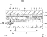
- FIG. 10 is a back plan view schematically showing two solar cells, a wiring member, an insulating member, and a connecting member included in a solar cell panel according to yet still another embodiment of the invention.
- a connection structure of first and second wirings 22a and 22b, first and second electrodes 142 and 144, and first and second connection portions CP1 and CP2 in a first solar cell 10a is the same as a connection structure of first and second wirings 22a and 22b, first and second electrodes 142 and 144, and first and second connection portions CP1 and CP2 in a second solar cell 10b.
- the first wiring 22a is electrically connected to the first electrode 142 and is insulated from the second electrode 144
- the second wiring 22b is electrically connected to the second electrode 144 and is insulated from the first electrode 142.
- a connection wiring 24 is provided between the first solar cell 10a and the second solar cell 10b.
- the connection wiring 24 is positioned in a direction (a first direction) crossing a wiring member 22 and connected to the wiring member 22.
- a plurality of solar cells 10 can be connected in a second direction (an x-axis direction in the drawing) by the wiring member 22 and the connection wiring 24 to form one row (i.e., a solar cell string).
- first wiring 22a connected to the first electrode 142 of the first solar cell 10a and the second wiring 22b connected to the second electrode 144 of the second solar cell 10b are overlapped and connected to the connection wiring 24 extending in the first direction crossing the first and second wirings 22a and 22b.
- the first solar cell 10a and the second solar cell 10b can be connected in series in the second direction.
- the first and second wirings 22a and 22b and the connection wirings 24 are separately formed and electrically connected to each other.
- the first and second wirings 22a and 22b and the connection wirings 24 may be connected to each other by a conductive material layer (not shown).
- the conductive material layer may be the same material as the connecting member 32 or may be a different material.
- the connection wiring 24 may have the same material or structure as the wiring member 22 and/or a bus bar wiring 26 (refer to FIG. 1 ), or may have a different material or structure from the wiring member 22 and/or a bus bar wiring 26.
- first partial wirings 221a and 222a and a plurality of second partial wirings 221b and 222b are all shorter than the length of each solar cell 10 in the second direction, and thus, a length of each portion of the wiring member 22 can be minimized.
Abstract
Description
- This application claims the priority benefit of Korean Patent Application No.
10-2017-0105559 - Embodiments of the invention relate to a solar cell panel, and, more particularly, to a solar cell panel having an improved structure.
- Recently, as existing energy resources such as petroleum and coal are expected to be depleted, interest in alternative energy to replace them is increasing. Among them, solar cells are attracting attention as a next-generation battery that converts solar energy into electric energy.
- A plurality of such solar cells are connected in series or in parallel by a wiring and are manufactured in a form of a solar cell panel by a packaging process for protecting the plurality of solar cells. Since a solar cell panel generates electricity for a long time in various environments, a solar cell panel is required to have long-term reliability. However, when expansion and contraction of a wiring for connecting a plurality of solar cells is repeated due to a change in temperature or the like, the wiring may be detached from a solar cell at a portion where adhesion is weak. As a result, an output of the solar cell panel is reduced, a defect rate is high, and long-term reliability may not be excellent.
- Therefore, embodiments of the invention have been made in view of the above problems, and embodiments of the invention are to provide a solar cell panel having a high output, a low defect rate, and excellent long-term reliability.
- A solar cell panel according to an embodiment of the invention includes a plurality of solar cells including a first solar cell and a second solar cell, and a wiring portion extending in a second direction crossing the first direction and electrically connecting the plurality of solar cells. Each of the plurality of solar cells includes a plurality of first electrodes and a plurality of second electrodes extending in a first direction. The wiring portion includes a first wiring connected to the plurality of first electrodes of the first solar cell, the first wiring includes a plurality of first partial wirings in the second direction in the first solar cell, and the plurality of first partial wirings are different members from each other and are electrically connected to each other by a first connection portion on the first solar cell.
- According to an embodiment, a problem caused by expansion and contraction of a wiring member can be solved by using a wiring member composed of a plurality of partial wirings having a relatively short length. Accordingly, it is possible to prevent an output reduction of a solar cell panel and deterioration or a defect of the solar cell panel and to improve long-term reliability of the solar cell panel. Also, a structure of the wiring member connecting electrodes having different polarities in neighboring first and second solar cells can be simplified by differentiating an arrangement of the electrodes and connection portions in the first and second solar cells. Particularly, when electrodes having different polarities in the first and second solar cells are connected together by a common wiring, a connection structure can be simplified and an interval between the first and second solar cells can be reduced. Accordingly, efficiency of the solar cell panel can be greatly improved.
-
-
FIG. 1 is an exploded perspective view schematically showing a solar cell panel according to an embodiment of the invention. -
FIG. 2 is a cross-sectional view showing an example of a solar cell included in the solar cell panel shown inFIG. 1 . -
FIG. 3 is a back plan view schematically showing two solar cells, a wiring member, an insulating member, and a connecting member included in the solar cell panel shown inFIG. 1 . -
FIG. 4 is a cross-sectional view showing the solar cell panel taken along line IV-IV ofFIG. 3 . -
FIG. 5 is a back plan view schematically showing a solar cell panel according to another embodiment of the invention. -
FIG. 6 is a partial cross-sectional view showing a solar cell panel according to yet another embodiment of the invention. -
FIG. 7 is a back plan view schematically showing two solar cells, a wiring member, an insulating member, and a connecting member included in a solar cell panel according to still another embodiment of the invention. -
FIG. 8 is a cross-sectional view showing the solar cell panel taken along line VIII-VIII ofFIG. 7 . -
FIG. 9 is a cross-sectional view showing a solar cell panel according to a modified embodiment of the invention. -
FIG. 10 is a back plan view schematically showing two solar cells, a wiring member, an insulating member, and a connecting member included in a solar cell panel according to yet still another embodiment of the invention. - Reference will now be made in detail to various embodiments of the invention, examples of which are illustrated in accompanying drawings. The invention may, however, be embodied in many alternate forms and should not be construed as limited to the embodiments set forth herein.
- In the drawings, illustration of parts unrelated to embodiments of the invention is omitted for clarity and simplicity of description. The same reference numerals designate the same or very similar elements throughout the specification. In the drawings, thicknesses, widths or the like of elements are exaggerated or reduced for clarity of description, and should not be construed as limited to those illustrated in the drawings.
- It will be understood that the terms "comprise" and/or "comprising," or "include" and/or "including" used in the specification specify the presence of stated elements, but do not preclude the presence or addition of one or more other elements. In addition, it will be understood that, when an element such as a layer, film, region, or plate is referred to as being "on" another element, it may be directly disposed on another element or may be disposed such that an intervening element is also therebetween. Accordingly, when an element such as a layer, film, region, or plate is disposed "directly on" another element, this means that there is no intervening element between the elements.
- Hereinafter, a solar cell panel according to an embodiment of the invention will be described in detail with reference to the accompanying drawings.
-
FIG. 1 is an exploded perspective view schematically showing a solar cell panel according to an embodiment of the invention, andFIG. 2 is a cross-sectional view showing an example of a solar cell included in the solar cell panel shown inFIG. 1 . For reference,FIG. 2 is a cross-sectional view showing the solar cell taken along line II-II inFIG. 3 . - Referring to
FIGS. 1 and2 , asolar cell panel 100 according to the embodiment includes a plurality ofsolar cells 10 and awiring portion 20 for electrically connecting the plurality ofsolar cells 10. Thesolar cell panel 100 includes asealing member 44 that surrounds and seals thesolar cells 10 and thewiring portion 20, afirst member 42a positioned on a front surface of thesolar cells 10 on the sealingmember 44, and aback member 42b positioned on a back surface of thesolar cells 10 on the sealingmember 44. This will be described in more detail. In this instance, thesolar cell 10 may include asemiconductor substrate 110 and afirst electrode 142 and asecond electrode 144 disposed on one surface (e.g., a back surface) of thesemiconductor substrate 110. This will be described in detail later with reference toFIG. 2 . - In the embodiment, the
solar cell panel 100 may include a plurality ofsolar cells 10, and the plurality ofsolar cells 10 may be electrically connected in series, parallel, or series-parallel by awiring portion 20. - More specifically, the
wiring portion 20 may include awiring member 22. At least a part of thewiring member 22 may overlap the first orsecond electrodes solar cell 10 to be connected to the first orsecond electrodes solar cells 10 may be connected in one direction (an x-axis direction in the drawings) by thewiring member 22 to form one row (i.e., a solar cell string). Thewiring portion 20 may further include abus bar wiring 26 positioned at both ends of the solar cell string and connecting a solar cell string to another solar cell string or a junction box (not shown). - The
wiring member 22 or thebus bar wiring 26 may each include a conductive material (for example, a metal material). For example, thewiring member 22 or thebus bar wiring 26 may include a conductive core including any one of gold (Au), silver (Ag), copper (Cu), and aluminum (Al), and a conductive coating layer that is disposed on a surface of the conductive core and includes tin (Sn) or an alloy including tin. In one example, the conductive core may be formed of copper (Cu), and the conductive coating layer may be formed of SnBiAg, which is an alloy including tin. However, embodiments of the invention are not limited thereto, and a material, a shape, a connection structure, etc. of thewiring member 22 or thebus bar wiring 26 may be variously modified. - The sealing
member 44 may include afirst sealing member 44a positioned on front surfaces ofsolar cells 10 connected by thewiring portion 20 and asecond sealing member 44b positioned on back surfaces of thesolar cells 10 connected by thewiring portion 20. Thefirst sealing member 44a and the second sealingmember 44b prevent moisture and oxygen from entering and chemically bind elements of thesolar cell panel 100. The first and second sealingmembers first sealing member 44a or thesecond sealing member 44b. Theback member 42b, thesecond sealing member 44b, thesolar cells 10, thewiring portion 20, a shield member 50, and thefirst sealing member 44a, and thefront member 42a may be integrated to constitute thesolar cell panel 100 through a lamination process using the first andsecond sealing members - The
front member 42a is disposed on the first sealingmember 44a to constitute a front surface of thesolar cell panel 100 and theback member 42b is disposed on thesecond sealing member 44b to constitute a back surface of thesolar cell panel 100. Thefront member 42a and theback member 42b may be made of an insulating material capable of protecting thesolar cells 10 from external shock, moisture, ultraviolet rays, or the like. Thefront member 42a may be made of a light-transmitting material capable of transmitting light, and theback member 42b may be made of a sheet made of a light-transmitting material, a non-light-transmitting material, or a reflective material. For example, thefront member 42a may be formed of a glass substrate or the like, and theback member 42b may be formed of a film or a sheet. Theback member 42b may have a TPT (Tedlar / PET / Tedlar) type or a polyvinylidene fluoride (PVDF) resin layer formed on at least one surface of a base film (for example, polyethylene terephthalate, PET). - However, embodiments of the invention are not limited thereto. Accordingly, the first or second sealing
member front member 42a, or theback member 42b may include any of various materials other than those described above, and may have any of various shapes. For example, thefront member 42a or theback member 42b may have any of various forms (e.g., a substrate, a film, a sheet, etc.) or any of various materials. - Referring to
FIG. 2 , an example of asolar cell 10 included in thesolar cell panel 100 according to the embodiment of the invention will be described in more detail. - Referring to
FIG. 2 , thesolar cell 10 according to the embodiment includes a photoelectric conversion portion including asemiconductor substrate 110, and first andsecond electrodes second electrodes first electrode 142 and thesecond electrode 144 may be formed parallel to each other while being positioned together on one surface (e.g., a back surface) of the photoelectric conversion portion. Thus, thesolar cell 10 may have a back contact structure. - In the embodiment, the photoelectric conversion portion may include the
semiconductor substrate 110 and aconductive region semiconductor substrate 110. In the embodiment, a firstconductive region 132 and a secondconductive region 134 that are involved in carriers having polarities opposite to each other may be positioned on one surface (e.g., the back surface) of thesemiconductor substrate 110. In this instance, the first and secondconductive regions semiconductor substrate 110 by acontrol passivation layer 120 interposed therebetween. - In one example, the
semiconductor substrate 110 may include abase region 112 made of a crystalline semiconductor (for example, a single-crystalline or a polycrystalline semiconductor, as an example, a single-crystalline or a polycrystalline silicon wafer, particularly, a single-crystalline silicon wafer) doped with a second conductive type dopant. Thesolar cell 10 based on thesemiconductor substrate 110 or thebase region 112 having a high degree of crystallinity and having few defects has excellent electrical properties. A front surface field region 114 having the same conductivity type as thebase region 112 and having a higher doping concentration than thebase region 112 may be positioned on or at the front surface of thesemiconductor substrate 110. An anti-reflection structure (for example, a pyramid-shaped texturing structure including a (111) surface of the semiconductor substrate 110) for preventing reflection may be formed at the front surface of thesemiconductor substrate 110, while the back surface of thesemiconductor substrate 110 may be a mirror-polished surface or may have a smaller surface roughness than the front surface. However, embodiments of the invention are not limited thereto and various modifications are possible. - The
control passivation layer 120 may be formed of an oxide layer, a dielectric layer or an insulating layer including silicon, an oxynitride layer, an oxycarbonate layer, or the like. As an example, thecontrol passivation layer 120 may be a silicon oxide layer. - The first and second
conductive regions conductive regions - In this instance, an area (for example, a width) of the first
conductive region 132 may be larger than an area (for example, a width) of the secondconductive region 134. The firstconductive region 132 serving as an emitter region has a larger area than the secondconductive region 134 serving as a back surface field region, which is advantageous for photoelectric conversion. In the embodiment, the first and secondconductive regions semiconductor layer 130 to be positioned in the same plane, and abarrier region 136 formed of an intrinsic semiconductor, which is not doped, may be provided between the first and secondconductive regions - However, embodiments of the invention are not limited thereto. Therefore, the
control passivation layer 120 may not be provided. Alternatively, at least one of the first and secondconductive regions semiconductor substrate 110 to constitute a part of thesemiconductor substrate 110. Also, thebarrier region 136 may be not provided, or thebarrier region 136 may include a material other than a semiconductor material or may be formed of an empty space. Various other variations are possible. - A
front passivation layer 124 and/or ananti-reflection layer 126 is entirely formed on the front surface of the semiconductor substrate 110 (more particularly, on the front surface field region 114 formed on or at the front surface of the semiconductor substrate 110). Aback passivation layer 140 may be entirely positioned on the back surface of thesemiconductor layer 130 except for acontact hole 140a. For example, thefront passivation layer 124, theanti-reflection layer 126, or theback passivation layer 140 may include one layer of a silicon nitride layer, a silicon nitride layer including hydrogen, a silicon oxide layer, a silicon oxynitride layer, an aluminum oxide layer, a silicon carbide layer, MgF2, ZnS, TiO2, and CeO2, or a multi-layered structure which two or more layers including at least one of the above are stacked. - The
first electrode 142 is electrically connected to (e.g., in contact with) the firstconductive region 132 through thecontact hole 140a and thesecond electrode 144 is electrically connected to (e.g., in contact with) the secondconductive region 134 through thecontact hole 140a. Thefirst electrode 142 and thesecond electrode 144 may be formed of a conductive material (e.g., a metal). In the embodiment, thesolar cell 10 may further include apad electrode FIG. 3 ), which will be described later in more detail with reference toFIGS. 3 and4 . - The
solar cell 10 is electrically connected to anothersolar cell 10 by thewiring portion 20 including thewiring member 22. Hereinafter, a structure of thesolar cell 10 and thewiring portion 20 will be described in more detail with reference toFIGS. 3 and4 . -
FIG. 3 is a back plan view schematically showing twosolar cells 10, awiring member 22, an insulatingmember 34, and a connectingmember 32 included in thesolar cell panel 100 shown inFIG. 1 .FIG. 4 is a cross-sectional view showing thesolar cell panel 100 taken along line IV-IV ofFIG. 3 . Twosolar cells 10 adjacent to each other are referred to as a firstsolar cell 10a and a secondsolar cell 10b in the following description for clear distinction. - Referring to
FIGS. 1 to 4 , afirst electrode 142 of a firstsolar cell 10a and asecond electrode 144 of a secondsolar cell 10b are electrically connected by a plurality ofwiring members 22. - More particularly, in each of the first and second
solar cells first electrode 142 may include a plurality offirst electrodes 142 longitudinally extending in a first direction (a y-axis direction in the drawings), and thesecond electrode 144 may include a plurality ofsecond electrodes 144 longitudinally extending in the first direction. In addition, thefirst electrodes 142 and thesecond electrodes 144 may be alternately disposed in a second direction (an x-axis direction in the drawings) crossing the first direction. - In this instance, the first and second
conductive regions second electrodes conductive region 132 may include a plurality of portions extending in the first direction to correspond to the plurality offirst electrodes 142. The secondconductive region 134 may include a plurality of portions extending in the first direction to correspond to the plurality ofsecond electrodes 144. However, the first and secondconductive regions second electrodes barrier region 136 may be positioned between the firstconductive region 132 and the secondconductive region 134. However, embodiments of the invention are not limited thereto, and the first and secondconductive regions second electrodes - In this instance, the
wiring member 22 in each of the first and secondsolar cells first wiring 22a connected to one of the first andsecond electrodes second wiring 22b connected to the other of thesecond electrodes - In this specification, the
wiring members 22 positioned at one same position (for example, a first position PI) in the first direction in the first and secondsolar cells first wirings 22a, and thewiring members 22 positioned at another same position different from the first position PI in the first direction (for example, the second position P2) are referred to assecond wirings 22b. In eachsolar cell 10, any one of the first andsecond wirings first electrode 142 through the connectingmember 32 and is insulated from thesecond electrode 144 through the insulatingmember 34, and the other one of the first andsecond wirings second electrode 144 through the connectingmember 32 and is insulated from thefirst electrode 142 through the insulatingmember 34. The plurality offirst wirings 22a and the plurality ofsecond wirings 22b are provided in thesolar cell 10, and thefirst wirings 22a and thesecond wirings 22b are alternately positioned in the first direction. Then, the plurality of first andsecond wirings second electrodes - The connecting
member 32 may include any of various conductive materials, and the insulatingmember 34 may include any of various insulating materials. For example, the connectingmember 32 may be formed of a material included in the first andsecond electrodes wiring member 22, or a mixed material including the material included in the first andsecond electrodes wiring member 22. For example, the connectingmember 32 may include the material included in the first andsecond electrodes wiring member 22 by a process where thewiring member 22 is placed on the first andsecond electrodes member 32 may include a solder paste layer, an epoxy solder paste layer, or the like. As an example, the connectingmember 32 may include a low-temperature solder paste layer and a high-temperature solder paste layer together. The insulatingmember 34 may include any of a silicone-based resin, an epoxy-based resin, a urethane-based resin, an acryl-based resin, polyimide, polyethylene, and the like. - In the embodiment, the
first wiring 22a may extend in the second direction to overlap the plurality offirst electrodes 142 to be connected to the plurality offirst electrodes 142 in the firstsolar cell 10a. Also, thesecond wiring 22b may extend in the second direction to overlap the plurality ofsecond electrodes 144 to be connected to the plurality ofsecond electrodes 144 in the firstsolar cell 10a. In this instance, in the firstsolar cell 10a, thefirst wiring 22a extends to one side (a right side inFIG. 3 and4 ) of the firstsolar cell 10a in the second direction and is electrically connected to the secondsolar cell 10b positioned at the one side (the right side inFIG. 3 and4 ) of the firstsolar cell 10a, and thesecond wiring 22b extends to the other side (a left side inFIGS. 3 and4 ) of the firstsolar cell 10a and is electrically connected to a solar cell 10 (that is, a third solar cell) positioned at the other side (the left side inFIGS. 3 and4 ) of the firstsolar cell 10a. - As a result, in the first
solar cell 10a, the connectingmembers 32 may be positioned between thefirst wiring 22a and the plurality offirst electrodes 142 at portions where thefirst wiring 22a and the plurality offirst electrodes 142 overlap each other, and the insulatingmembers 34 may be positioned between thefirst wiring 22a and the plurality ofsecond electrodes 144 at portions where thefirst wiring 22a and the plurality ofsecond electrodes 144 overlap each other. Also, in the firstsolar cell 10a, the connectingmembers 32 may be positioned between thesecond wiring 22b and the plurality ofsecond electrodes 144 at portions where thesecond wiring 22b and the plurality ofsecond electrodes 144 overlap each other, and the insulatingmembers 34 may be positioned between thesecond wiring 22b and the plurality offirst electrodes 142 at portions where thesecond wiring 22b and the plurality offirst electrodes 142 overlap each other. - In this instance, the
first wiring 22a may include a plurality of firstpartial wirings partial wirings solar cell 10a. The plurality of firstpartial wirings first wiring 22a may be positioned at the same position in the first direction and extend in the second direction. Then, a length of each of the firstpartial wirings first wirings 22a can be reduced, and thus, a problem that may occur when a length of thefirst wirings 22a or lengths of the firstpartial wirings first wirings 22a are large can be prevented. - More particularly, when temperature changes in an environment where the
solar cell panel 100 is positioned, expansion and contraction of the wiring member 22 (that is, the first andsecond wirings wiring member 22 may be separated from thesolar cell 10 or thewiring member 22 may be damaged or torn by the expansion and contraction of thewiring member 22. Such a problem may become more serious as the length of thewiring member 22 becomes larger. If such a problem occurs, thesolar cell panel 100 may be judged as defective and an output of thesolar cell panel 100 may be lowered. Particularly, in a structure in which the first andsecond electrodes wiring member 22 are positioned only on one surface of thesolar cell 10 as in the embodiment, the problem caused by the expansion and contraction of thewiring member 22 may be more serious. - In view of this, in the embodiment, the problem caused by the expansion and contraction of the
wiring member 22 can be prevented by using thefirst wiring 22a composed of the plurality of firstpartial wirings solar cell panel 100 and deterioration or a defect of thesolar cell panel 100 and to improve long-term reliability of thesolar cell panel 100. - The plurality of first
partial wirings internal wiring 221a positioned only in the firstsolar cell 10a and at least one firstextended wiring 222a electrically connected to the firstinternal wiring 221a and extending from a side adjacent to the firstinternal wiring 221a to an outside of one side (a right side inFIGS. 3 and4 ) of the firstsolar cell 10a. - For example, with respect to one
first wiring 22a of the first solar cell 1 0a, one firstinternal wiring 221a is provided and one firstextended wiring 222a is provided, and one first connection portion CP1 where the firstinternal wiring 221a and the firstextended wiring 222a are connected is provided in the firstsolar cell 10a. Thus, a number of the plurality of firstpartial wirings first wirings 22a can be simplified. However, embodiments of the invention are not limited thereto. At least two firstinternal wirings 221a may be provided in the firstsolar cell 10a. In this instance, a number of the first connection portions CP1 may be equal to a number of the firstinternal wirings 221a. In this instance, lengths of the firstinternal wirings 221a and intervals of the first connection portions CP1 may be uniform or may be different from each other. - In this instance, the first connection portion CP1 may be positioned at a central portion of the first
solar cell 10a in the second direction. Then, the firstinternal wiring 221a and the firstextended wiring 222a are symmetrically positioned in the firstsolar cell 10a, and a problem caused by thermal stress can be minimized. However, embodiments of the invention are not limited to this, and the first connection portion CP1 may be positioned at a part other than the central portion of the firstsolar cell 10a. - In the drawing, it is exemplified that each of a plurality of
first wirings 22a includes a plurality of firstpartial wirings partial wirings first wirings 22a may include a plurality of firstpartial wirings first wirings 22a are positioned at the same position in the first direction. However, embodiments of the invention are not limited thereto, and at least twofirst wires 22a having the first connection portions CP1 at different positions may be provided. - In the embodiment, the first connection portion CP1 may be a
first pad electrode 224a formed on the firstsolar cell 10a. That is, the plurality of firstpartial wirings first pad electrode 224a, respectively, so that the plurality of firstpartial wirings FIGS. 3 and4 , it is exemplified that a part of each of the plurality of firstpartial wirings first pad electrode 224a. In this instance, as shown inFIG. 4 , theconnection members 32 may be positioned between the plurality of firstpartial wirings first pad electrodes 224a so that the plurality of firstpartial wirings first pad electrodes 224a are electrically and physically connected to each other. However, embodiments of the invention are not limited thereto. Therefore, the firstpartial wirings first pad electrodes 224a may be melted using a soldering process without the connectingmembers 32, thereby connecting the firstpartial wirings first pad electrodes 224a. Various other variations are possible. - In this instance, the
first pad electrode 224a is positioned on an insulating layer (that is, the back passivation layer 140). Thus, thefirst pad electrode 224a may be a floating electrode being spaced apart from thesemiconductor substrate 110 and the first and secondconductive regions first pad electrode 224a may be involved only in the connection between the plurality of firstpartial wirings conductive regions first pad electrode 224a may be connected to the firstconductive region 132 through the insulating layer. Then, thefirst pad electrode 224a may be formed together with thefirst electrode 142 to simplify a process. Alternatively, thefirst pad electrode 224a may be an electrode extended from thefirst electrode 142. Various other variations are possible. - The
first pad electrode 224a may be formed of any of various materials having conductivity (e.g., a metal). Thefirst pad electrode 224a may be formed of the same material as the first and/orsecond electrodes 142 and/or 144, or may be formed of different materials from the first and/orsecond electrodes 142 and/or 144. - In the drawings, it is exemplified that a width of the
first pad electrode 224a in the first direction is larger than a width of thefirst wiring 22a (that is, widths of the plurality of firstpartial wirings partial wirings first pad electrode 224a to minimize the length of the plurality of firstpartial wirings first pad electrode 224a in the first direction may be equal to or smaller than the width of thefirst wiring 22a (that is, the widths of the plurality of firstpartial wirings partial wirings first pad electrode 224a. Various other variations are possible. - Similarly, the
second wiring 22b may include a plurality of secondpartial wirings partial wirings solar cell 10a. The plurality of secondpartial wirings second wiring 22b may be positioned at the same position in the first direction and extend in the second direction. Then, a length of each of the secondpartial wirings second wirings 22b can be reduced, and thus, a problem that may occur when a length of thesecond wirings 22b or lengths of the secondpartial wirings second wirings 22b are large can be prevented. Accordingly, it is possible to prevent an output reduction of thesolar cell panel 100 and deterioration or a defect of thesolar cell panel 100 and to improve long-term reliability of thesolar cell panel 100. - In this instance, the plurality of second
partial wirings internal wiring 221b positioned only in the firstsolar cell 10a and at least one secondextended wiring 222b electrically connected to the secondinternal wiring 221b and extending from a side adjacent to the secondinternal wiring 221b to an outside of the other side (a left side inFIGS. 3 and4 ) of the firstsolar cell 10a. - For example, with respect to one
second wiring 22b of the firstsolar cell 10a, one secondinternal wiring 221b is provided and one secondextended wiring 222b is provided, and one second connection portion CP2 where the secondinternal wiring 221b and the secondextended wiring 222b are connected is provided in the firstsolar cell 10a. However, embodiments of the invention are not limited thereto. At least two secondinternal wirings 221b may be provided in the firstsolar cell 10a. In this instance, a number of the second connection portions CP2 may be equal to a number of the secondinternal wirings 221b. In this instance, lengths of the secondinternal wirings 221b and intervals of the second connection portions CP2 may be uniform or may be different from each other. - In this instance, the second connection portion CP2 may be positioned at a central portion of the first
solar cell 10a in the second direction. However, embodiments of the invention are not limited to this, and the second connection portion CP2 may be positioned at a part other than the central portion of the firstsolar cell 10a. - In the drawing, it is exemplified that each of a plurality of
second wirings 22b includes a plurality of secondpartial wirings partial wirings second wirings 22b may include a plurality of secondpartial wirings second wirings 22b are positioned at the same position in the second direction. However, embodiments of the invention are not limited thereto, and at least twosecond wires 22b having the second connection portions CP2 at different positions may be provided. - In the embodiment, the second connection portion CP2 may be a
second pad electrode 224b formed on the firstsolar cell 10a. That is, the plurality of secondpartial wirings second pad electrode 224b, respectively, so that the plurality of secondpartial wirings FIGS. 3 and4 , it is exemplified that a part of each of the plurality of secondpartial wirings second pad electrode 224b. Theconnection members 32 may be positioned between the plurality of secondpartial wirings second pad electrodes 224b. Alternatively, the secondpartial wirings second pad electrodes 224b may be melted using a soldering process without the connectingmembers 32, thereby connecting the secondpartial wirings second pad electrodes 224b. Various other variations are possible. - In this instance, the
second pad electrode 224b is positioned on an insulating layer (that is, the rear passivation layer 140). Thus, thesecond pad electrode 224b may be a floating electrode being spaced apart from thesemiconductor substrate 110 and the second and secondconductive regions second pad electrode 224b may be involved only in the connection between the plurality of secondpartial wirings second pad electrode 224b may be connected to the secondconductive region 132 through the insulating layer. Then, thesecond pad electrode 224b may be formed together with thesecond electrode 142 to simplify a process. - The
second pad electrode 224b may be formed of any of various materials having conductivity (e.g., a metal). Thesecond pad electrode 224b may be formed of the same material as the first and/orsecond electrodes 142 and/or 144, or may be formed of different materials from the first and/orsecond electrodes 142 and/or 144. - In
FIG. 3 , it is exemplified that a width of thesecond pad electrode 224b in the first direction is larger than a width of thesecond wiring 22b (that is, widths of the plurality of secondpartial wirings partial wirings second pad electrode 224b to minimize the length of the plurality of secondpartial wirings second pad electrode 224b in the first direction may be equal to or smaller than the width of thesecond wiring 22b (that is, the widths of the plurality of secondpartial wirings partial wirings second pad electrode 224b. Various other variations are possible. - As described above, the
first wirings 22a and thesecond wirings 22b may be alternately arranged in the first direction. More specifically, in a portion adjacent to the one side (e.g., the right side inFIG. 3 ) of the firstsolar cell 10a, the firstextended wirings 222a and the secondinternal wirings 221b may be alternatively positioned in the first direction. In the other portion, the firstinternal wirings 221a and the secondextended wirings 222b may alternately be positioned in the first direction. As a result, the secondsolar cell 10b and the third solar cell positioned on both sides of the firstsolar cell 10a in the second direction can be electrically connected in series to the firstsolar cell 10. InFIG. 3 , the first pad electrode 424a and the second pad electrode 424b are positioned at the same positions when viewed in the second direction, but embodiments of the invention are not limited thereto. - In the embodiment, a connection structure of the first and
second wirings second electrodes solar cell 10b positioned adjacent to the one side of the firstsolar cell 10a may be different from that in the firstsolar cell 10a. The above description of the first andsecond wirings second electrodes solar cell 10a may be applied as it is to the first andsecond wirings second electrodes solar cell 10b, except for the connection structure. - More specifically, in the second
solar cell 10b, thefirst wiring 22a is electrically connected to thesecond electrode 144, and thesecond wiring 22b is electrically connected to thefirst electrode 142. In contrast to the firstsolar cell 10a, in the secondsolar cell 10b, the firstinternal wiring 221a is positioned on the one side (the right side inFIGS. 3 and4 ) of the secondsolar cell 10b, and the firstextended wiring 222a extends to the other side (the left side inFIGS. 3 and4 ) of the secondsolar cell 10b. In contrast to the firstsolar cell 10a, in the secondsolar cell 10b, the secondinternal wiring 221b is positioned on the other side of the secondsolar cell 10b and the secondextended wiring 222b extends to the one side of the secondsolar cell 10b. Accordingly, in a portion adjacent to the one side (e.g., the right side inFIG. 3 ) of the secondsolar cell 10b, the firstinternal wirings 221a and the secondextended wirings 222b may be alternatively positioned in the first direction. In the other portion, the firstextended wirings 222a and the secondinternal wirings 221b may alternately be positioned in the first direction. Also, thefirst wirings 22a and thesecond wirings 22b are alternatively positioned in the first direction in the secondsolar cell 10b; however, it is contrary to an arrangement in the firstsolar cell 10a. That is, when viewed in the first direction, an order of the first connection portion CP1 and the second connection portion CP2 is repeated in the firstsolar cell 10a, while an order of the second connection portion CP2 and the first connection portion CP1 is repeated in the secondsolar cell 10b. - When the first and
second wirings electrodes solar cells first electrode 142 of the firstsolar cell 10a and thesecond electrode 144 of the secondsolar cell 10b are electrically connected to each other by connecting thefirst wiring 22a of the firstsolar cell 10a and thefirst wiring 22a of the secondsolar cell 10b. Also, thesecond electrode 144 of the firstsolar cell 10a and thefirst electrode 142 of another solar cell 10 (that is, a third solar cell 10) positioned on the other side (the left side ofFIG. 3 ) of the firstsolar cell 10a are electrically connected to each other by connecting thesecond wiring 22b of the firstsolar cell 10a and thesecond wiring 22b of the thirdsolar cell 10. Further, thefirst electrode 142 of the secondsolar cell 10b and thesecond electrode 144 of other solar cell 10 (that is, a fourth solar cell 10) positioned on the one side (the right side ofFIG. 3 ) of the secondsolar cell 10b are electrically connected to each other by connecting thesecond wiring 22b of the firstsolar cell 10a and thesecond wiring 22b of the fourthsolar cell 10. That is, the plurality ofsolar cells 10 can be electrically connected with each other by connecting thefirst wirings 22a positioned at the same first position PI in the first direction in the two neighboringsolar cells 10 with each other and connecting thesecond wirings 22b positioned at the same second position P2 in the first direction in the two neighboringsolar cells 10 with each other. Thus, the plurality ofsolar cells 10 can be electrically connected with each other by an easy and simple structure. - In one example, the first
extended wiring 222a of the firstsolar cell 10a and the firstextended wiring 222a of the secondsolar cell 10b, which are positioned at the same position in the first direction, are formed of a single first common wiring CW1 having a single body having an elongated structure. The first common wiring CW1 extends from the first connection portion CP1 of the firstsolar cell 10a to the second connection portion CP2 of the secondsolar cell 10b through a space between the firstsolar cell 10a and the secondsolar cell 10b. In this instance, the first common wiring CW1 is connected to thefirst electrode 142 in the firstsolar cell 10a and is connected to thesecond electrode 144 in the secondsolar cell 10b. Then, a total number of thefirst wirings 22a formed of the plurality of firstpartial wirings solar cells wiring portion 20 can be simplified. - Similarly, the second
extended wiring 222b of the firstsolar cell 10a and the secondextended wiring 222b of the thirdsolar cell 10 that is positioned at the other side (the left side ofFIG. 3 ), which are positioned at the same position in the first direction, are formed of a single second common wiring CW2 having a single body having an elongated structure. The second common wiring CW2 extends from the second connection portion CP2 of the firstsolar cell 10a to the second connection portion CP2 of the thirdsolar cell 10 through a space between the firstsolar cell 10a and the thirdsolar cell 10. In this instance, the second common wiring CW2 is connected to thesecond electrode 144 in the firstsolar cell 10a and is connected to thefirst electrode 142 in the thirdsolar cell 10. - Also, the second
extended wiring 222b of the secondsolar cell 10b and the secondextended wiring 222b of the fourthsolar cell 10 that is positioned at the one side (the right side ofFIG. 3 ), which are positioned at the same position in the first direction, are formed of a single second common wiring CW2 having a single body having an elongated structure. The second common wiring CW2 extends from the first connection portion CP1 of the secondsolar cell 10b to the second connection portion CP2 of the fourthsolar cell 10 through a space between the secondsolar cell 10b and the fourthsolar cell 10. In this instance, the second common wiring CW2 is connected to thefirst electrode 142 in the secondsolar cell 10b and is connected to thesecond electrode 144 in the fourthsolar cell 10. - On the other hand, when the first wiring is connected to the
first electrode 142 only and the second wiring is connected to thesecond electrode 144 only in eachsolar cell 10, an additional or separate wiring or structure for connecting the first wiring of the firstsolar cell 10a and the second wiring of the secondsolar cell 10b is required. For example, an additional wiring, which is formed in a direction crossing the first andsecond wirings connection wiring 24 shown inFIG. 10 ) between the firstsolar cell 10a and the secondsolar cell 10b, or the like are required. - In the embodiment, the above-described additional or separate wiring or the structure or the additional wiring formed in the direction crossing the first and
second wirings wiring portion 20, a material cost, and the like can be reduced. In addition, an interval between the firstsolar cell 10a and the secondsolar cell 10b can be reduced, and efficiency of thesolar cell panel 100 can be improved. Also, end portions of the plurality of firstpartial wirings partial wirings partial wirings partial wirings members 32 closely or densely positioned, and therefore, fixing stability of the plurality of firstpartial wirings partial wirings - In this instance, in the embodiment, after the same
solar cells 10 are manufactured in plural, onesolar cell 10 is used as the firstsolar cell 10a as it is, and the other neighboringsolar cell 10 is rotated 180 degrees and is used as the secondsolar cell 10b. That is, the firstsolar cell 10a and the secondsolar cell 10b may be symmetric in origin. Such a pair of first and secondsolar cells solar cells 10 can be formed. - Thus, alignment marks 50a or 50b having the same shape may be positioned at different positions in the first
solar cell 10a and the secondsolar cell 10b. For example, afirst alignment mark 50a is positioned at an upper left side ofFIG. 3 and asecond alignment mark 50b is positioned at a lower right side ofFIG. 3 in the firstsolar cell 10a, while afirst alignment mark 50a is positioned at a lower right side ofFIG. 3 and asecond alignment mark 50b is positioned at an upper left side ofFIG. 3 in the secondsolar cell 10b. It can be seen that one of the first and secondsolar cells solar cells 10 can be manufactured by the same process, and the first or second common wiring CW1 or CW2 can be applied, thereby simplifying a manufacturing process. - According to the embodiment, a problem caused by expansion and contraction of the
wiring member 22 can be solved by using thewiring member 22 composed of the plurality of partial wirings 221a and 222a (221b and 222b) having a relatively short length. Accordingly, it is possible to prevent an output reduction of thesolar cell panel 100 and deterioration or a defect of thesolar cell panel 100 and to improve long-term reliability of thesolar cell panel 100. Also, a structure of thewiring member 22 connecting theelectrodes solar cells electrodes solar cells electrodes solar cells solar cells solar cell panel 100 can be greatly improved. - Although it is exemplified that the
first wiring 22a has the plurality of firstpartial wirings second wiring 22b has the plurality of secondpartial wirings second wirings wiring portions - Hereinafter, a solar cell panel according to other embodiments of the invention will be described in detail. The detailed description will be omitted for the same or extremely similar parts as the above description, and only the different parts will be described in detail. It is also within the scope of the invention to combine the above-described embodiment or variations thereof with the following embodiments or variations thereof.
-
FIG. 5 is a back plan view schematically showing a solar cell panel according to another embodiment of the invention. For reference, a portion corresponding to the enlarged portion ofFIG. 3 is shown inFIG. 5 . - Referring to
FIG. 5 , in the embodiment, anauxiliary connecting member 32a is positioned at a portion spaced apart from afirst pad electrode 224a and adjacent to an end portion of a firstinternal wiring 221a adjacent to thefirst pad electrode 224a. Thereby, an adhesion force of the firstinternal wiring 221a can be further improved. The auxiliary connectingmember 32a is a connecting member positioned on an insulating layer (that is, a back passivation layer 140) at a portion where first andsecond electrodes member 32a may be made of the same material as a connectingmember 32 or may be made of a different material from the connectingmember 32. - An end portion of the first
extended wiring 222a adjacent to thefirst pad electrode 224a is connected and fixed by the connectingmember 32 on thefirst electrode 142 at a portion spaced apart from thefirst pad electrode 224a and adjacent to the end portion of the firstextended wiring 222a. Thus, an adhesion force of the firstextended wiring 222a can be further improved. In this instance, since an auxiliary connectingmember 32a for the firstextended wiring 222a is not formed by using the connectingmember 32 positioned on thefirst electrode 142 as it is, it is possible to reduce a material cost and simplify a process. However, embodiments of the invention are not limited thereto. Therefore, anauxiliary connecting member 32a may be further positioned at the end portion of the firstextended wiring 222a. Alternatively, the connectingmember 32 may be positioned at the end portion of the firstinternal wiring 221a and the auxiliary connectingmember 32a may be positioned at the end portion of the firstextended wiring 222a. Various other variations are possible. - As described above, the connecting
member 32 or the auxiliary connectingmember 32a is positioned at the portion spaced apart from thefirst pad electrode 224a and adjacent to the end portions of the firstpartial wirings first pad electrode 224a. Thus, the adhesion force of the plurality of firstpartial wirings - Similarly, a connecting
member 32 or an auxiliary connectingmember 32a is positioned at each of portions spaced apart from asecond pad electrode 224b and adjacent to end portions of a plurality of secondpartial wirings second pad electrode 224b. An adhesion force of the secondpartial wirings first pad electrode 224a and thesecond pad electrode 224b in a second direction are different from each other and thus at least one end portions of the plurality of firstpartial wirings partial wirings member 32 to minimize a number of auxiliary connectingmembers 32a. However, embodiments of the invention are not limited thereto. -
FIG. 6 is a partial cross-sectional view showing a solar cell panel according to yet another embodiment of the invention. For reference, a portion corresponding toFIG. 4 is shown inFIG. 6 . - Referring to
FIG. 6 , in the embodiment, a plurality of firstpartial wirings first wiring 22a include a first overlappingportion 226a where the plurality of firstpartial wirings partial wirings portion 226a to form the first connection portion CP1. Although it is not shown in the drawing, a plurality of second partial wirings constituting a second wiring may overlap each other (for example, in contact with each other) and electrically connected to each other at a second overlapping portion for constituting a second connection portion. When the plurality of firstpartial wirings - Alternatively, a separate adhesive layer, an adhesive material, or the like for adhering the first
partial wirings partial wirings portion 226a or the second overlapping portion may be further provided. -
FIG. 7 is a back plan view schematically showing two solar cells, a wiring member, an insulating member, and a connecting member included in a solar cell panel according to still another embodiment of the invention, andFIG. 8 is a cross-sectional view showing the solar cell panel taken along line VIII-VIII ofFIG. 7 . - Referring to
FIGS. 7 and8 , in the embodiment, a fixingmember 28 for fixing a plurality of firstpartial wirings partial wirings partial wirings - For example, the fixing
member 28 may be formed to entirely cover portions of the plurality of firstpartial wirings member 28 can fix or attach at least the plurality of firstpartial wirings solar cell 10. - In the embodiment, fixing stability of the plurality of first and/or second
partial wirings partial wirings member 28. Thus, it is possible to prevent the firstpartial wirings partial wirings wiring member 22. The first and/or secondpartial wirings member 28 so that the sealingmember 44 is spaced from the first and second connection portions CP1 and CP2 with the fixingmember 28 therebetween at a surface where the fixingmember 28 is positioned. Then, the sealingmaterial 44 cannot penetrate between thesolar cell 10 and the plurality of first or secondpartial wirings second wirings solar cell panel 100 and deterioration or a defect of thesolar cell panel 100 and to improve long-term reliability of thesolar cell panel 100. - In this instance, a width of the fixing
member 28 in the second direction may be equal to or greater than a width of the first and second connection portions CP1 and CP2. Then, the fixingmember 28 is formed to entirely and stably overlap a portion of first or secondpartial wirings member 28 can be maximized. - In this instance, the fixing
member 28 may include any of various materials capable of fixing the first andsecond wirings member 28 may be formed of an insulating tape including abase member 28a and an attachinglayer 28b which is positioned on one surface of thebase member 28a and connected to thewiring portion 20. When the fixingmember 28 is made of a tape, the fixingmember 28 can be fixed at a desired position by a simple process of attaching the tape. - The
base member 28a serves to increase a strength of the fixingmember 28. For example, thebase member 28a may be made of a resin as a main component. For example, thebase member 28a may include at least one of polyethylene (PE), polyethylene terephthalate (PET), and the like. - The attaching
layer 28b may be fixed to thewiring member 22 by adhesion or cohesion, including an adhesive material or a cohesive material. Here, the term of "adhesion" means that two layers are attached to each other through a heat-treatment and thus one of the two layers is damaged when the two layers are separated. The term of "cohesion" means that two layers are attached and separated at a room temperature by a predetermined physical force without being damaged. When the attachinglayer 28b includes the adhesive material, it can have better fixing properties. When the attachinglayer 28b includes the cohesive material, the fixingmember 28 can be easily detached when the fixingmember 28 is attached incorrectly or when thesolar cell 10 is replaced or repaired. For example, the attachinglayer 28b may include an adhesive material or an cohesive material of an epoxy-based material, an acryl-based material, or a silicone-based material. Also, the fixingmember 28 is not formed of an insulating tape but may be formed by applying or coating an adhesive material or a cohesive material. - In the drawings, the fixing
member 28 has a shape extending along a first direction and partially positioned at a central portion in a second direction in which the first and second connection portions CP1 and CP2 are positioned to entirely cover the first and second connection portions CP1 and CP2. According to this, fixing stability of the first orsecond wiring portions member 28 corresponding to the first and second connection portions CP1 and CP2 may be separately formed. Various other variations are possible. - In
FIGS. 7 and8 , the first and second connection portions CP1 and CP2 are formed of first andsecond pad electrodes FIG. 3 . However, embodiments of the invention are not limited thereto. Therefore, as shown inFIG. 9 , a fixingmember 28 is applied when the first and/or second connection portions CP1 and/or CP2 are formed of overlapped portions where a plurality offirst wiring portions second wiring portions -
FIG. 10 is a back plan view schematically showing two solar cells, a wiring member, an insulating member, and a connecting member included in a solar cell panel according to yet still another embodiment of the invention. - Referring to
FIG. 10 , in the embodiment, a connection structure of first andsecond wirings second electrodes solar cell 10a is the same as a connection structure of first andsecond wirings second electrodes solar cell 10b. Thus, in the each of the first and secondsolar cells first wiring 22a is electrically connected to thefirst electrode 142 and is insulated from thesecond electrode 144, and thesecond wiring 22b is electrically connected to thesecond electrode 144 and is insulated from thefirst electrode 142. - A
connection wiring 24 is provided between the firstsolar cell 10a and the secondsolar cell 10b. Theconnection wiring 24 is positioned in a direction (a first direction) crossing awiring member 22 and connected to thewiring member 22. A plurality ofsolar cells 10 can be connected in a second direction (an x-axis direction in the drawing) by thewiring member 22 and theconnection wiring 24 to form one row (i.e., a solar cell string). - More specifically, the
first wiring 22a connected to thefirst electrode 142 of the firstsolar cell 10a and thesecond wiring 22b connected to thesecond electrode 144 of the secondsolar cell 10b are overlapped and connected to theconnection wiring 24 extending in the first direction crossing the first andsecond wirings solar cell 10a and the secondsolar cell 10b can be connected in series in the second direction. In the drawing, it is exemplified that the first andsecond wirings second wirings member 32 or may be a different material. Theconnection wiring 24 may have the same material or structure as thewiring member 22 and/or a bus bar wiring 26 (refer toFIG. 1 ), or may have a different material or structure from thewiring member 22 and/or abus bar wiring 26. - Since the
wirings solar cell 10 have the same arrangement, thesolar cells 10 having thewirings connection wiring 24. Thus, it is possible to easily manufacture a solar cell string. In addition, a plurality of firstpartial wirings partial wirings internal wirings extended wirings solar cell 10 in the second direction, and thus, a length of each portion of thewiring member 22 can be minimized. - The features, structures, effects and the like according to the above-described embodiments are included in at least one embodiment of the invention and are not necessarily limited to one embodiment. Further, the features, structures, effects and the like illustrated in the embodiments can be combined and modified by other persons skilled in the art to which the embodiments belong. Therefore, it is to be understood that embodiments of the invention are not limited to these embodiments.
Claims (15)
- A solar cell panel comprising:a plurality of solar cells including a first solar cell and a second solar cell, each of the plurality of solar cells including a plurality of first electrodes and a plurality of second electrodes extending in a first direction; anda wiring portion extending in a second direction crossing the first direction and electrically connecting the plurality of solar cells to each other,wherein the wiring portion includes a first wiring of the first solar cell, the first wiring being connected to the plurality of first electrodes of the first solar cell,wherein the first wiring of the first solar cell includes a plurality of first partial wirings of the first solar cell in the second direction in the first solar cell, andwherein the plurality of first partial wirings of the first solar cell are separated from each other and are electrically connected to each other by a first connection portion on the first solar cell.
- The solar cell panel according to claim 1, wherein the plurality of first partial wirings of the first solar cell are located at a same position in the first direction.
- The solar cell panel according to claim 1 or 2, wherein the plurality of first partial wirings of the first solar cell includes a first internal wiring in the first solar cell and a first extended wiring of the first solar cell that extends outside of the first solar cell.
- The solar cell panel according to claim 3, wherein at least one of the following is fulfilled for the first wiring:wherein each of the first wiring of the first solar cell includes one first internal wiring disposed in the first solar cell and one first extended wiring extending to the outside of the first solar cell; andwherein the first connection portion on the first solar cell is positioned at a central portion of the first solar cell in the second direction.
- The solar cell panel according to claim 3, wherein the second solar cell includes a first wiring of the second solar cell and positioned at a same position in the first direction as the first wiring of the first solar cell,
wherein the first wiring of the second solar cell is electrically connected to the second electrode of the second solar cell, and
wherein the first extended wiring of the first solar cell longitudinally extends in the second direction and is connected to the second electrode of the second solar cell. - The solar cell panel according to claim 5, wherein the first wiring of the second solar cell includes a first internal wiring in the second solar cell and a first extended wiring of the second solar call that extends outside of the second solar cell, and
wherein the first extended wiring of the first solar cell and the first extended wiring of the second solar cell are formed of a first common wiring having a single body extending in the second direction. - The solar cell panel according to claim 6, wherein at least one of the following is fulfilled for the first solar cell and the second solar cell:wherein each of the first solar cell and the second solar cell has an alignment mark, wherein the alignment mark of the first solar cell has a shape the same as the alignment mark of the second solar cell, and wherein the alignment marks having the same shape of the first solar cell and the second solar cell are positioned at different positions in the first solar cell and the second solar cell; andwherein the first solar cell and the second solar cell are symmetrically arranged.
- The solar cell panel according to one of preceeding claims, wherein the first connection portion on the first solar cell includes a first pad electrode among a plurality of first pad electrodes formed on the first solar cell, and
wherein the plurality of first partial wirings of the first solar cell are connected to the first pad electrode. - The solar cell panel according to claim 8, wherein a width of the first pad electrode of the first solar cell in the first direction is larger than a width of a corresponding first partial wiring among the plurality of first partial wirings of the first solar call, and
wherein the plurality of first partial wirings of the first solar cell are spaced apart from each other on corresponding first pad electrodes among the plurality of first pad electrodes. - The solar cell panel according to claim 8, wherein the first solar cell comprises a semiconductor substrate, and the plurality of first electrodes in the first solar cell and the plurality of second electrodes in the first solar cell are formed on the semiconductor substrate, and
wherein the first pad electrode of the first solar cell comprises a floating electrode spaced apart from the semiconductor substrate. - The solar cell panel according to one of preceeding claims, wherein the plurality of first partial wirings of the first solar cell overlap each other to be electrically connected at the first connection portion on the first solar cell.
- The solar cell panel according to claim 11, wherein the plurality of first partial wirings are electrically and physically connected to each other at the first connection portion on the first solar cell.
- The solar cell panel according to one of preceeding claims, further comprising:a fixing member fixing the plurality of first partial wirings of the first solar cell at the first connection portion on the first solar cell, andwherein the fixing member is formed of an insulating tape.
- The solar cell panel according to one of preceeding claims, wherein the first solar cell and the second solar cell are electrically connected to each other without a wiring formed in a direction crossing the first wiring of the first solar cell.
- The solar cell panel according to one of preceeding claims, wherein the wiring portion includes a second wiring connected to the plurality of second electrodes of the first solar cell,
wherein the second wiring includes a plurality of second partial wirings in the second direction in the first solar cell,
wherein the plurality of second partial wirings are separated from each other and are electrically connected to each other by a second connection portion on the first solar cell,
wherein, in the first solar cell, the plurality of second partial wirings includes a second internal wiring disposed in the first solar cell and a second extended wiring extending outside of the first solar cell, and
wherein the first extended wiring and the second internal wiring are alternately positioned in the first direction or the second extended wiring and the first internal wiring in the first solar cell are alternately positioned in the first direction.
Applications Claiming Priority (1)
| Application Number | Priority Date | Filing Date | Title |
|---|---|---|---|
| KR1020170105559A KR102374145B1 (en) | 2017-08-21 | 2017-08-21 | Solar cell panel |
Publications (2)
| Publication Number | Publication Date |
|---|---|
| EP3447805A1 true EP3447805A1 (en) | 2019-02-27 |
| EP3447805B1 EP3447805B1 (en) | 2020-06-17 |
Family
ID=63311872
Family Applications (1)
| Application Number | Title | Priority Date | Filing Date |
|---|---|---|---|
| EP18189676.2A Active EP3447805B1 (en) | 2017-08-21 | 2018-08-20 | Solar cell panel |
Country Status (5)
| Country | Link |
|---|---|
| US (1) | US11101397B2 (en) |
| EP (1) | EP3447805B1 (en) |
| JP (1) | JP7283870B2 (en) |
| KR (1) | KR102374145B1 (en) |
| CN (1) | CN109560147B (en) |
Cited By (1)
| Publication number | Priority date | Publication date | Assignee | Title |
|---|---|---|---|---|
| EP4068396A1 (en) * | 2021-03-30 | 2022-10-05 | Golden Solar (Quanzhou) New Energy Technology Co., Ltd. | Welding method for welding strip of back-contact solar cell chip |
Families Citing this family (1)
| Publication number | Priority date | Publication date | Assignee | Title |
|---|---|---|---|---|
| WO2021117740A1 (en) * | 2019-12-11 | 2021-06-17 | 株式会社カネカ | Solar battery cell, solar battery device, and solar battery module |
Citations (3)
| Publication number | Priority date | Publication date | Assignee | Title |
|---|---|---|---|---|
| US3819417A (en) * | 1972-05-17 | 1974-06-25 | Communications Satellite Corp | Mechanically interlaced and electrically interconnected silicon solar cells |
| US20100116323A1 (en) * | 2006-01-27 | 2010-05-13 | Yoshio Katayama | Interconnector, Solar Cell String Using the Interconnector and Method of Manufacturing Thereof, and Solar Cell Module, Using The Solar Cell String |
| US20160035907A1 (en) * | 2014-08-04 | 2016-02-04 | Lg Electronics Inc. | Solar cell module |
Family Cites Families (21)
| Publication number | Priority date | Publication date | Assignee | Title |
|---|---|---|---|---|
| JP5171001B2 (en) | 2005-09-30 | 2013-03-27 | 三洋電機株式会社 | Method for manufacturing solar cell module, solar cell and solar cell module |
| JP4684075B2 (en) * | 2005-10-14 | 2011-05-18 | シャープ株式会社 | Solar cell, solar cell string and solar cell module |
| JP2009176782A (en) * | 2008-01-21 | 2009-08-06 | Sanyo Electric Co Ltd | Solar cell module |
| JP2010141206A (en) | 2008-12-12 | 2010-06-24 | Sanyo Electric Co Ltd | Solar cell module and replacing method for solar cell |
| JP5378424B2 (en) | 2010-01-22 | 2013-12-25 | シャープ株式会社 | Solar cell with wiring sheet, solar cell module, and method for manufacturing solar cell with wiring sheet |
| KR20130086960A (en) * | 2010-05-28 | 2013-08-05 | 솔라월드 이노베이션즈 게엠베하 | Method for contacting and connecting solar cells and solar cell combination produced by means of said method |
| JP5232213B2 (en) | 2010-12-03 | 2013-07-10 | シャープ株式会社 | Back electrode type solar cell, solar cell module, solar cell wafer, and method for manufacturing solar cell module |
| KR101356216B1 (en) * | 2012-01-18 | 2014-01-28 | 참엔지니어링(주) | Method for processing a substrate of solar cell |
| EP2704213A1 (en) | 2012-08-30 | 2014-03-05 | Komax Holding AG | Method and apparatus for connecting solar cells to a solar cell string and solar cell string |
| DE102013212845A1 (en) * | 2013-07-02 | 2015-01-08 | Solarworld Industries Sachsen Gmbh | photovoltaic module |
| KR101661948B1 (en) * | 2014-04-08 | 2016-10-04 | 엘지전자 주식회사 | Solar cell and method for manufacturing the same |
| PL2966693T3 (en) * | 2014-07-07 | 2023-07-10 | Shangrao Jinko Solar Technology Development Co., Ltd | Solar cell module |
| KR101757879B1 (en) * | 2014-08-04 | 2017-07-26 | 엘지전자 주식회사 | Solar cell module |
| KR101820103B1 (en) | 2014-10-27 | 2018-01-18 | 엘지전자 주식회사 | Solar cell module and Methods and Apparatus thereof |
| KR101889842B1 (en) * | 2014-11-26 | 2018-08-20 | 엘지전자 주식회사 | Solar cell module |
| JP6455099B2 (en) * | 2014-11-27 | 2019-01-23 | 日立化成株式会社 | Solar cell unit and method for manufacturing solar cell unit |
| US11532765B2 (en) * | 2015-04-30 | 2022-12-20 | Shangrao Jinko Solar Technology Development Co., Ltd | Solar cell and solar cell panel including the same |
| US10217877B2 (en) | 2015-07-27 | 2019-02-26 | Lg Electronics Inc. | Solar cell |
| JP6307131B2 (en) * | 2015-09-08 | 2018-04-04 | エルジー エレクトロニクス インコーポレイティド | Solar cell module and manufacturing method thereof |
| JP2017069442A (en) * | 2015-09-30 | 2017-04-06 | パナソニックIpマネジメント株式会社 | Solar battery module |
| CN106784051A (en) | 2017-01-22 | 2017-05-31 | 泰州乐叶光伏科技有限公司 | Carry high-power IBC batteries interconnection architecture |
-
2017
- 2017-08-21 KR KR1020170105559A patent/KR102374145B1/en active IP Right Grant
-
2018
- 2018-08-20 JP JP2018153791A patent/JP7283870B2/en active Active
- 2018-08-20 EP EP18189676.2A patent/EP3447805B1/en active Active
- 2018-08-21 US US16/107,599 patent/US11101397B2/en active Active
- 2018-08-21 CN CN201810952461.7A patent/CN109560147B/en active Active
Patent Citations (3)
| Publication number | Priority date | Publication date | Assignee | Title |
|---|---|---|---|---|
| US3819417A (en) * | 1972-05-17 | 1974-06-25 | Communications Satellite Corp | Mechanically interlaced and electrically interconnected silicon solar cells |
| US20100116323A1 (en) * | 2006-01-27 | 2010-05-13 | Yoshio Katayama | Interconnector, Solar Cell String Using the Interconnector and Method of Manufacturing Thereof, and Solar Cell Module, Using The Solar Cell String |
| US20160035907A1 (en) * | 2014-08-04 | 2016-02-04 | Lg Electronics Inc. | Solar cell module |
Cited By (1)
| Publication number | Priority date | Publication date | Assignee | Title |
|---|---|---|---|---|
| EP4068396A1 (en) * | 2021-03-30 | 2022-10-05 | Golden Solar (Quanzhou) New Energy Technology Co., Ltd. | Welding method for welding strip of back-contact solar cell chip |
Also Published As
| Publication number | Publication date |
|---|---|
| JP7283870B2 (en) | 2023-05-30 |
| JP2019036733A (en) | 2019-03-07 |
| KR20190020510A (en) | 2019-03-04 |
| CN109560147A (en) | 2019-04-02 |
| EP3447805B1 (en) | 2020-06-17 |
| US11101397B2 (en) | 2021-08-24 |
| US20190058072A1 (en) | 2019-02-21 |
| CN109560147B (en) | 2022-05-27 |
| KR102374145B1 (en) | 2022-03-15 |
Similar Documents
| Publication | Publication Date | Title |
|---|---|---|
| EP3142156B1 (en) | Solar cell module and method for manufacturing the same | |
| JP6046658B2 (en) | Solar cell | |
| CN110379870B (en) | Solar cell module and method for manufacturing same | |
| EP3163630B1 (en) | Solar cell module | |
| KR101816164B1 (en) | Solar cell module | |
| US11538950B2 (en) | Solar cell panel | |
| KR20140003691A (en) | Solar cell module and ribbon assembly | |
| US11177406B2 (en) | Solar cell and solar cell module using the same | |
| EP3447805B1 (en) | Solar cell panel | |
| JP2024037993A (en) | How to manufacture solar panels | |
| US10879412B2 (en) | Solar cell panel | |
| KR101890288B1 (en) | Solar cell and solar cell panel including the same | |
| KR102483637B1 (en) | Solar cell panel | |
| KR20190014882A (en) | Solar cell panel and method for manufacturing the same | |
| US11489083B2 (en) | Solar cell panel | |
| KR101816155B1 (en) | Solar cell panel | |
| KR101806972B1 (en) | Solar cell module | |
| KR101788166B1 (en) | Solar cell module | |
| KR102496629B1 (en) | Solar cell panel | |
| KR20190049215A (en) | Solar cell panel | |
| KR20190061365A (en) | Solar cell panel | |
| KR101816151B1 (en) | Solar cell module | |
| KR101806981B1 (en) | Solar cell module | |
| KR20190050560A (en) | Solar cell panel | |
| KR20190006358A (en) | Solar cell and solar cell panel including the same |
Legal Events
| Date | Code | Title | Description |
|---|---|---|---|
| PUAI | Public reference made under article 153(3) epc to a published international application that has entered the european phase |
Free format text: ORIGINAL CODE: 0009012 |
|
| STAA | Information on the status of an ep patent application or granted ep patent |
Free format text: STATUS: THE APPLICATION HAS BEEN PUBLISHED |
|
| AK | Designated contracting states |
Kind code of ref document: A1 Designated state(s): AL AT BE BG CH CY CZ DE DK EE ES FI FR GB GR HR HU IE IS IT LI LT LU LV MC MK MT NL NO PL PT RO RS SE SI SK SM TR |
|
| AX | Request for extension of the european patent |
Extension state: BA ME |
|
| STAA | Information on the status of an ep patent application or granted ep patent |
Free format text: STATUS: REQUEST FOR EXAMINATION WAS MADE |
|
| 17P | Request for examination filed |
Effective date: 20190702 |
|
| RBV | Designated contracting states (corrected) |
Designated state(s): AL AT BE BG CH CY CZ DE DK EE ES FI FR GB GR HR HU IE IS IT LI LT LU LV MC MK MT NL NO PL PT RO RS SE SI SK SM TR |
|
| GRAP | Despatch of communication of intention to grant a patent |
Free format text: ORIGINAL CODE: EPIDOSNIGR1 |
|
| STAA | Information on the status of an ep patent application or granted ep patent |
Free format text: STATUS: GRANT OF PATENT IS INTENDED |
|
| INTG | Intention to grant announced |
Effective date: 20200224 |
|
| RAP1 | Party data changed (applicant data changed or rights of an application transferred) |
Owner name: LG ELECTRONICS INC. |
|
| RIN1 | Information on inventor provided before grant (corrected) |
Inventor name: HYUN, DAESEON Inventor name: YANG, HYEYOUNG |
|
| GRAS | Grant fee paid |
Free format text: ORIGINAL CODE: EPIDOSNIGR3 |
|
| GRAA | (expected) grant |
Free format text: ORIGINAL CODE: 0009210 |
|
| STAA | Information on the status of an ep patent application or granted ep patent |
Free format text: STATUS: THE PATENT HAS BEEN GRANTED |
|
| AK | Designated contracting states |
Kind code of ref document: B1 Designated state(s): AL AT BE BG CH CY CZ DE DK EE ES FI FR GB GR HR HU IE IS IT LI LT LU LV MC MK MT NL NO PL PT RO RS SE SI SK SM TR |
|
| REG | Reference to a national code |
Ref country code: GB Ref legal event code: FG4D |
|
| REG | Reference to a national code |
Ref country code: CH Ref legal event code: EP |
|
| REG | Reference to a national code |
Ref country code: DE Ref legal event code: R096 Ref document number: 602018005327 Country of ref document: DE |
|
| REG | Reference to a national code |
Ref country code: IE Ref legal event code: FG4D |
|
| REG | Reference to a national code |
Ref country code: AT Ref legal event code: REF Ref document number: 1282395 Country of ref document: AT Kind code of ref document: T Effective date: 20200715 |
|
| PG25 | Lapsed in a contracting state [announced via postgrant information from national office to epo] |
Ref country code: SE Free format text: LAPSE BECAUSE OF FAILURE TO SUBMIT A TRANSLATION OF THE DESCRIPTION OR TO PAY THE FEE WITHIN THE PRESCRIBED TIME-LIMIT Effective date: 20200617 Ref country code: GR Free format text: LAPSE BECAUSE OF FAILURE TO SUBMIT A TRANSLATION OF THE DESCRIPTION OR TO PAY THE FEE WITHIN THE PRESCRIBED TIME-LIMIT Effective date: 20200918 Ref country code: FI Free format text: LAPSE BECAUSE OF FAILURE TO SUBMIT A TRANSLATION OF THE DESCRIPTION OR TO PAY THE FEE WITHIN THE PRESCRIBED TIME-LIMIT Effective date: 20200617 Ref country code: NO Free format text: LAPSE BECAUSE OF FAILURE TO SUBMIT A TRANSLATION OF THE DESCRIPTION OR TO PAY THE FEE WITHIN THE PRESCRIBED TIME-LIMIT Effective date: 20200917 Ref country code: LT Free format text: LAPSE BECAUSE OF FAILURE TO SUBMIT A TRANSLATION OF THE DESCRIPTION OR TO PAY THE FEE WITHIN THE PRESCRIBED TIME-LIMIT Effective date: 20200617 |
|
| REG | Reference to a national code |
Ref country code: LT Ref legal event code: MG4D |
|
| REG | Reference to a national code |
Ref country code: NL Ref legal event code: MP Effective date: 20200617 |
|
| PG25 | Lapsed in a contracting state [announced via postgrant information from national office to epo] |
Ref country code: HR Free format text: LAPSE BECAUSE OF FAILURE TO SUBMIT A TRANSLATION OF THE DESCRIPTION OR TO PAY THE FEE WITHIN THE PRESCRIBED TIME-LIMIT Effective date: 20200617 Ref country code: RS Free format text: LAPSE BECAUSE OF FAILURE TO SUBMIT A TRANSLATION OF THE DESCRIPTION OR TO PAY THE FEE WITHIN THE PRESCRIBED TIME-LIMIT Effective date: 20200617 Ref country code: LV Free format text: LAPSE BECAUSE OF FAILURE TO SUBMIT A TRANSLATION OF THE DESCRIPTION OR TO PAY THE FEE WITHIN THE PRESCRIBED TIME-LIMIT Effective date: 20200617 Ref country code: BG Free format text: LAPSE BECAUSE OF FAILURE TO SUBMIT A TRANSLATION OF THE DESCRIPTION OR TO PAY THE FEE WITHIN THE PRESCRIBED TIME-LIMIT Effective date: 20200917 |
|
| REG | Reference to a national code |
Ref country code: AT Ref legal event code: MK05 Ref document number: 1282395 Country of ref document: AT Kind code of ref document: T Effective date: 20200617 |
|
| PG25 | Lapsed in a contracting state [announced via postgrant information from national office to epo] |
Ref country code: NL Free format text: LAPSE BECAUSE OF FAILURE TO SUBMIT A TRANSLATION OF THE DESCRIPTION OR TO PAY THE FEE WITHIN THE PRESCRIBED TIME-LIMIT Effective date: 20200617 Ref country code: AL Free format text: LAPSE BECAUSE OF FAILURE TO SUBMIT A TRANSLATION OF THE DESCRIPTION OR TO PAY THE FEE WITHIN THE PRESCRIBED TIME-LIMIT Effective date: 20200617 |
|
| PG25 | Lapsed in a contracting state [announced via postgrant information from national office to epo] |
Ref country code: IT Free format text: LAPSE BECAUSE OF FAILURE TO SUBMIT A TRANSLATION OF THE DESCRIPTION OR TO PAY THE FEE WITHIN THE PRESCRIBED TIME-LIMIT Effective date: 20200617 Ref country code: RO Free format text: LAPSE BECAUSE OF FAILURE TO SUBMIT A TRANSLATION OF THE DESCRIPTION OR TO PAY THE FEE WITHIN THE PRESCRIBED TIME-LIMIT Effective date: 20200617 Ref country code: SM Free format text: LAPSE BECAUSE OF FAILURE TO SUBMIT A TRANSLATION OF THE DESCRIPTION OR TO PAY THE FEE WITHIN THE PRESCRIBED TIME-LIMIT Effective date: 20200617 Ref country code: PT Free format text: LAPSE BECAUSE OF FAILURE TO SUBMIT A TRANSLATION OF THE DESCRIPTION OR TO PAY THE FEE WITHIN THE PRESCRIBED TIME-LIMIT Effective date: 20201019 Ref country code: AT Free format text: LAPSE BECAUSE OF FAILURE TO SUBMIT A TRANSLATION OF THE DESCRIPTION OR TO PAY THE FEE WITHIN THE PRESCRIBED TIME-LIMIT Effective date: 20200617 Ref country code: EE Free format text: LAPSE BECAUSE OF FAILURE TO SUBMIT A TRANSLATION OF THE DESCRIPTION OR TO PAY THE FEE WITHIN THE PRESCRIBED TIME-LIMIT Effective date: 20200617 Ref country code: ES Free format text: LAPSE BECAUSE OF FAILURE TO SUBMIT A TRANSLATION OF THE DESCRIPTION OR TO PAY THE FEE WITHIN THE PRESCRIBED TIME-LIMIT Effective date: 20200617 Ref country code: CZ Free format text: LAPSE BECAUSE OF FAILURE TO SUBMIT A TRANSLATION OF THE DESCRIPTION OR TO PAY THE FEE WITHIN THE PRESCRIBED TIME-LIMIT Effective date: 20200617 |
|
| PG25 | Lapsed in a contracting state [announced via postgrant information from national office to epo] |
Ref country code: SK Free format text: LAPSE BECAUSE OF FAILURE TO SUBMIT A TRANSLATION OF THE DESCRIPTION OR TO PAY THE FEE WITHIN THE PRESCRIBED TIME-LIMIT Effective date: 20200617 Ref country code: PL Free format text: LAPSE BECAUSE OF FAILURE TO SUBMIT A TRANSLATION OF THE DESCRIPTION OR TO PAY THE FEE WITHIN THE PRESCRIBED TIME-LIMIT Effective date: 20200617 Ref country code: IS Free format text: LAPSE BECAUSE OF FAILURE TO SUBMIT A TRANSLATION OF THE DESCRIPTION OR TO PAY THE FEE WITHIN THE PRESCRIBED TIME-LIMIT Effective date: 20201017 |
|
| REG | Reference to a national code |
Ref country code: DE Ref legal event code: R097 Ref document number: 602018005327 Country of ref document: DE |
|
| PG25 | Lapsed in a contracting state [announced via postgrant information from national office to epo] |
Ref country code: MC Free format text: LAPSE BECAUSE OF FAILURE TO SUBMIT A TRANSLATION OF THE DESCRIPTION OR TO PAY THE FEE WITHIN THE PRESCRIBED TIME-LIMIT Effective date: 20200617 |
|
| PLBE | No opposition filed within time limit |
Free format text: ORIGINAL CODE: 0009261 |
|
| STAA | Information on the status of an ep patent application or granted ep patent |
Free format text: STATUS: NO OPPOSITION FILED WITHIN TIME LIMIT |
|
| PG25 | Lapsed in a contracting state [announced via postgrant information from national office to epo] |
Ref country code: LU Free format text: LAPSE BECAUSE OF NON-PAYMENT OF DUE FEES Effective date: 20200820 Ref country code: DK Free format text: LAPSE BECAUSE OF FAILURE TO SUBMIT A TRANSLATION OF THE DESCRIPTION OR TO PAY THE FEE WITHIN THE PRESCRIBED TIME-LIMIT Effective date: 20200617 |
|
| 26N | No opposition filed |
Effective date: 20210318 |
|
| REG | Reference to a national code |
Ref country code: BE Ref legal event code: MM Effective date: 20200831 |
|
| PG25 | Lapsed in a contracting state [announced via postgrant information from national office to epo] |
Ref country code: SI Free format text: LAPSE BECAUSE OF FAILURE TO SUBMIT A TRANSLATION OF THE DESCRIPTION OR TO PAY THE FEE WITHIN THE PRESCRIBED TIME-LIMIT Effective date: 20200617 |
|
| PG25 | Lapsed in a contracting state [announced via postgrant information from national office to epo] |
Ref country code: FR Free format text: LAPSE BECAUSE OF NON-PAYMENT OF DUE FEES Effective date: 20200831 |
|
| PG25 | Lapsed in a contracting state [announced via postgrant information from national office to epo] |
Ref country code: IE Free format text: LAPSE BECAUSE OF NON-PAYMENT OF DUE FEES Effective date: 20200820 Ref country code: BE Free format text: LAPSE BECAUSE OF NON-PAYMENT OF DUE FEES Effective date: 20200831 |
|
| REG | Reference to a national code |
Ref country code: CH Ref legal event code: PL |
|
| PG25 | Lapsed in a contracting state [announced via postgrant information from national office to epo] |
Ref country code: LI Free format text: LAPSE BECAUSE OF NON-PAYMENT OF DUE FEES Effective date: 20210831 Ref country code: CH Free format text: LAPSE BECAUSE OF NON-PAYMENT OF DUE FEES Effective date: 20210831 |
|
| PG25 | Lapsed in a contracting state [announced via postgrant information from national office to epo] |
Ref country code: TR Free format text: LAPSE BECAUSE OF FAILURE TO SUBMIT A TRANSLATION OF THE DESCRIPTION OR TO PAY THE FEE WITHIN THE PRESCRIBED TIME-LIMIT Effective date: 20200617 Ref country code: MT Free format text: LAPSE BECAUSE OF FAILURE TO SUBMIT A TRANSLATION OF THE DESCRIPTION OR TO PAY THE FEE WITHIN THE PRESCRIBED TIME-LIMIT Effective date: 20200617 Ref country code: CY Free format text: LAPSE BECAUSE OF FAILURE TO SUBMIT A TRANSLATION OF THE DESCRIPTION OR TO PAY THE FEE WITHIN THE PRESCRIBED TIME-LIMIT Effective date: 20200617 |
|
| PG25 | Lapsed in a contracting state [announced via postgrant information from national office to epo] |
Ref country code: MK Free format text: LAPSE BECAUSE OF FAILURE TO SUBMIT A TRANSLATION OF THE DESCRIPTION OR TO PAY THE FEE WITHIN THE PRESCRIBED TIME-LIMIT Effective date: 20200617 |
|
| REG | Reference to a national code |
Ref country code: DE Ref legal event code: R081 Ref document number: 602018005327 Country of ref document: DE Owner name: SHANGRAO JINKO SOLAR TECHNOLOGY DEVELOPMENT CO, CN Free format text: FORMER OWNER: LG ELECTRONICS INC., SEOUL, KR Ref country code: DE Ref legal event code: R082 Ref document number: 602018005327 Country of ref document: DE Representative=s name: DREISS PATENTANWAELTE PARTG MBB, DE Ref country code: DE Ref legal event code: R081 Ref document number: 602018005327 Country of ref document: DE Owner name: SHANGRAO XINYUAN YUEDONG TECHNOLOGY DEVELOPMEN, CN Free format text: FORMER OWNER: LG ELECTRONICS INC., SEOUL, KR |
|
| GBPC | Gb: european patent ceased through non-payment of renewal fee |
Effective date: 20220820 |
|
| PG25 | Lapsed in a contracting state [announced via postgrant information from national office to epo] |
Ref country code: GB Free format text: LAPSE BECAUSE OF NON-PAYMENT OF DUE FEES Effective date: 20220820 |
|
| PGFP | Annual fee paid to national office [announced via postgrant information from national office to epo] |
Ref country code: DE Payment date: 20230821 Year of fee payment: 6 |
|
| REG | Reference to a national code |
Ref country code: DE Ref legal event code: R081 Ref document number: 602018005327 Country of ref document: DE Owner name: SHANGRAO XINYUAN YUEDONG TECHNOLOGY DEVELOPMEN, CN Free format text: FORMER OWNER: SHANGRAO JINKO SOLAR TECHNOLOGY DEVELOPMENT CO., LTD, SHANGRAO, JIANGXI PROVINCE, CN |