EP3441797B1 - Sensorsystem - Google Patents
Sensorsystem Download PDFInfo
- Publication number
- EP3441797B1 EP3441797B1 EP18186409.1A EP18186409A EP3441797B1 EP 3441797 B1 EP3441797 B1 EP 3441797B1 EP 18186409 A EP18186409 A EP 18186409A EP 3441797 B1 EP3441797 B1 EP 3441797B1
- Authority
- EP
- European Patent Office
- Prior art keywords
- sensor
- mounting rail
- sensor housing
- contact
- housing
- Prior art date
- Legal status (The legal status is an assumption and is not a legal conclusion. Google has not performed a legal analysis and makes no representation as to the accuracy of the status listed.)
- Active
Links
Images

Classifications
-
- G—PHYSICS
- G01—MEASURING; TESTING
- G01V—GEOPHYSICS; GRAVITATIONAL MEASUREMENTS; DETECTING MASSES OR OBJECTS; TAGS
- G01V8/00—Prospecting or detecting by optical means
- G01V8/10—Detecting, e.g. by using light barriers
- G01V8/20—Detecting, e.g. by using light barriers using multiple transmitters or receivers
Definitions
- the present invention relates to a sensor system according to the preamble of claim 1.
- Such sensor systems are each from the DE 20 2014 102 335 U1 or the EP 2 208 092 B1 known.
- a disadvantage of the sensor systems mentioned is that the sensors are connected to one another via lines and cause effort during commissioning.
- the DE 20 2007 011 016 U1 discloses an optical sensor for detecting objects in a surveillance area, with at least one transmitter emitting light rays and at least one receiver receiving receiver light rays, the transmitter and / or receiver each being mounted in an integrally formed aperture tube, first parts of the aperture tube forming a light trap and further parts are provided for mounting an optic and / or for forming an aperture.
- An object of the invention is to provide an improved sensor system that can be put into operation very easily and that does not require a cable.
- a sensor system with a plurality of sensors, each with a sensor housing, the sensor housing being attachable to a mounting rail, the mounting rail having a flat contact element with at least two conductor tracks and the sensor housing each having at least two contact pins, the contact pins when the sensor is inserted into the mounting rail, each is connected to the conductor tracks of the planar contact element, the planar contact element having at least a third and a fourth conductor track, the third conductor track being provided for a ground connection and the fourth conductor track being provided for a supply voltage, on the flat one At least one contact element for each sensor housing a switching element for the conductor track of the supply voltage is provided, the respective switching element being actuable by an actuating means of the sensor housing.
- the invention enables a wireless arrangement of sensor housing with sensors, the integration of which takes place via the flat contact element and the mounting rail.
- the sensor housing has no cable connection and no plug / socket connection, but rather electrical contact pins that are connected directly to the conductor tracks of the flat contact element.
- the mounting rail has, on the one hand, a mechanical mount for the sensor housing and, on the other hand, the flat contact element with which the electrical connection to the sensor housing is established.
- the conductor tracks of the flat contact element can only be contacted, for example, in the area of the rear side of the sensor housing. The remaining area is, for example, insulated.
- the flat contact element contains the conductor tracks, which are covered with an insulating layer on each side. The conductor tracks are formed without insulation only at the points at which the conductor tracks are to be contacted.
- the mounting rail can be made of plastic or metal, for example.
- Plastic has the advantage here that the mounting rail itself is designed to be insulating.
- metallic mounting rails for example made of aluminum, can be made more stable than plastic rails.
- the mounting rail is manufactured using the extrusion process.
- the mounting rail can optionally also be made rigid.
- the contact pins protrude from the sensor housing, for example, so that they can contact the flat contact element as soon as the sensor housing is placed on the flat contact element and fastened on the mounting rail.
- the flat contact element is designed for a large number of position locations or slots for the sensor housing.
- the sensor housings can be freely arranged at a specific position. As a result, a freely selectable chain of sensors can be formed.
- the conductor tracks are arranged parallel to one another on the flat contact element.
- the power supply and the signal connection to the sensor housings and between the sensor housings are carried out, for example, via the conductor tracks.
- the flat contact element is a rigid circuit board or a contact foil.
- the contact foil is formed by a flexible, ie, flexible conductor foil.
- the contact film has the advantage that it can be stored on rolls and can be easily arranged in the mounting rail. Another advantage of the contact film is that it can be made very thin.
- the rigid circuit board is, for example, a circuit board. This has, for example, one or more layers. Rigid circuit boards can be made very robust, so that they are suitable for a variety of contacting processes.
- the mounting rail and the sensor housing each have mechanical latching means, as a result of which the sensor housing can be snapped into the mounting rail, as a result of which the sensor housing is mechanically fixed in the mounting rail.
- the sensor housing can be fastened to the mounting rail without additional, loose fastening means, such as, for example, screws.
- the mechanical latching means already predefine at least one predefined position of the sensor housing. Several predefined layers can also be provided, but correct contact is always guaranteed with the flat contact element.
- the sensor housing can also be removed if necessary.
- the mechanical locking means are released and the sensor housing can be removed again.
- the locking means or a locking mechanism consists, for example, of locking and spring elements on the sensor housing and on the mounting rail, so that the sensor housing can be snapped or snapped into the mounting rail. This ensures that the sensor housing is fixed to the mounting rail.
- the fixation could also be done magnetically.
- the sensor housings can snap into various predefined positions and be contacted with the conductor tracks of the mounting rail.
- the sensor housing can be used in a modified Kanban system.
- the sensor housing is clicked into the mounting rail and contacted.
- a current flow from the right or left can be possible.
- the sensor housing can also be used on driverless transport vehicles.
- the sensors can be clicked into a curved bumper.
- a light grid can be realized along the mounting rail with the sensor housings.
- the sensor housings are arranged in a certain grid at certain distances along the mounting rail. Only the positions on the mounting rail that are required are loaded.
- the sensor housing can also be used in a shelf system with a pick-to-light function, with a display showing a valid shelf compartment.
- the two conductor tracks are provided for two bus lines.
- the bus or bus system with two bus lines can be an available bus system according to the prior art. However, it can also be provided that an internal bus system is used.
- Available bus systems are, for example, CAN bus, Profibus, Interbus, ASI bus, Devicenet or similar bus systems.
- the flat contact element has at least a third and a fourth conductor track, the third conductor track being provided for a ground connection and the fourth conductor track being provided for a supply voltage.
- the voltage supply or power supply for the sensor housing is routed separately via the flat contact element.
- all the necessary connections of the sensor housing are made via the flat contact element.
- the conductor tracks for the energy supply are designed for the maximum current consumption of an overall system. Possibly. several conductor tracks are arranged in parallel to provide the energy supply.
- At least one switching element for the conductor path of the supply voltage is provided on the flat contact element for each sensor housing, the respective switching element being actuated by an actuating means of the sensor housing.
- the sensor housing has five electrical contact pins for the flat contact element.
- the flat contact element has five contact surfaces at every possible connection point to sensor housings.
- the five contact pins are two contact pins for the bus lines, one contact pin for the ground connection and two contact pins for the supply lines.
- the sensors can be initialized one after the other. Furthermore, the sensors can thereby be recognized, for example, among one another or identified in relation to a higher-level controller.
- a higher-level controller knows in which order the sensor housings are arranged.
- the individual control and evaluation units of the sensor housing can interrupt the energy supply locally before each start-up.
- a higher-level control and evaluation unit communicates, for example, with the first sensor or the first sensor housing. After an address assignment for the first sensor or the first sensor housing has taken place, the first sensor bridges the energy supply, so that communication with the second sensor takes place and an assignment or address assignment for the second sensor takes place in the same way.
- the other sensors are initialized accordingly.
- the contact pins of the sensor housing are designed, for example, as spring contact pins. Instead of the contact pins, contact can also be made, for example, with contact springs.
- the actuating means or the actuating element is provided on the sensor housing for interrupting the conductor track. By snapping the sensor housing into the mounting rail, the actuating element exerts a force on the switching element, which works as a switch.
- the actuating element can consist, for example, of several elements lined up, which are, for example, spring-mounted.
- the respective spring force is greater than the actuating force of the switch. This allows the sensor housing to be attached to the mounting rail without a grid.
- the switching element for example, which is designed as a make contact, is closed and the supply voltage is interrupted.
- the supply voltage is then closed again via an internal contact in the sensor housing.
- the switching element 12 can be an electromechanical switch.
- the switch opens again and the power line is closed again.
- the supply voltage line is not interrupted. I.e. the power supply to the next sensor housing is guaranteed.
- the power supply After plugging in the sensor housing, the power supply is interrupted and after addressing, the power supply is switched on.
- At least one switching element is provided per slot, even if the slot is not equipped with a sensor housing.
- the sensor housings can be repositioned or new sensor housings can be added.
- the voltage supply on the supply voltage line can take place at any point, so that the current can flow in both directions of the supply voltage line.
- the switching element is a break contact or a make contact.
- the break contact or make contact can, for example, be designed as a snap contact.
- An NC contact has the advantage that it can be used to directly interrupt the voltage or energy supply.
- a normally open contact can be provided, for example, in connection with a transistor in order to interrupt the voltage supply.
- a normally open contact has the advantage that the switch itself can be made simpler, since normally open contacts are easier to implement.
- a snap contact is designed as a make contact and an additional electronic circuit is provided to interrupt the voltage supply.
- the normally closed contact or normally open contact is formed, for example, by a metal dome, which functions as a switch.
- the switching elements can also be formed by metal balls which are held together by elastic elements, can be contacted by a contact pin and can be separated locally by the actuating means.
- the switching element is at least one field effect transistor or one field effect transistor stage.
- the break contact or the make contact can be realized by the at least one field effect transistor or the field effect transistor stage.
- the electromechanical switch can be part of a circuit, for example based on a transistor circuit, in particular with at least one field effect transistor or MOSFET transistor.
- a circuit with two field effect transistors is provided.
- the circuit allows current to flow in both directions.
- Further components, such as diodes, at least one resistor and at least one transistor are accommodated in the sensor housing.
- a field-effect transistor stage consisting of two field-effect transistors on the flat contact element or on the printed circuit board or a contact foil is used for switching the current path.
- the sensor closes the field effector transistor stage with a low-resistance resistor. After addressing has been completed, the current path is released again.
- the solution with field effect transistors is a solution that does not require a mechanical switch and is very inexpensive.
- An additional advantage is that the existing field effect transistor on the flat contact element is used for switching the voltage and the switching in the sensor is omitted. This means that a power switching element for a large current flow is no longer required in the sensor. Another advantage is that the current can flow from both directions.
- the sensors are one-way light barriers, reflection light barriers, light sensors and / or distance sensors.
- Distance sensors are based, for example, on the time-of-flight method, in which the light travel time is evaluated. Distance sensors can also work according to the principle of triangulation.
- a freely definable light curtain or a light curtain can be formed with any beam spacing, since the sensor housing can be arranged on the mounting rail at any spacing.
- one-way light barriers, reflection light barriers, light sensors and / or distance sensors can be arranged in any order and sequence in order to specifically implement specific applications. This enables a specially adaptable arrangement of sensors.
- the rail can also be made non-linear. That means e.g. bent with a certain radius.
- a central control and evaluation unit is provided which is connected to the sensor housing via the flat contact element.
- control and evaluation unit is then, like the sensor housing, also connected to the flat contact element via contact pins, the control and evaluation unit also being attached via the mounting rail.
- the sensor housing is constructed in two parts, with a first partial housing receiving the sensor elements and a second partial housing Has contact pins, wherein the first partial housing and the second partial housing are connected to one another via plug contacts.
- a plurality of mounting rails can be mechanically connected to one another or a plurality of flat contact elements can be electrically connected to one another.
- a cable with plugs is connected between flat contact elements.
- the flat contact element has holes or cutouts in order to ensure alignment of the sensor housing relative to the contact points or the switch.
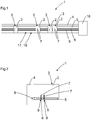
- Figure 1 shows a sensor system 1 with several sensors 2, each with a sensor housing 3, characterized in that the sensor housing 3 can be fastened to a mounting rail 4, the mounting rail 4 having a flat contact element 5 with at least two conductor tracks 6 and the sensor housing 3 each having at least two contact pins 7, wherein the contact pins 7 are each connected to the conductor tracks 6 of the flat contact element 5 when the sensor 2 is inserted into the receiving rail 4.
- the mounting rail is optionally rigid.
- the flat contact element 5 is a rigid circuit board 17 or a contact foil 18, in particular a flexible contact foil.
- sensors 2 can be arranged in any order and sequence.
- one-way light barriers, reflection light barriers, light scanners and / or distance sensors can be arranged in any order and sequence.
- a central control and evaluation unit 16 is provided which is connected to the sensor housings 3 via the flat contact element 5.
- control and evaluation unit 16 is also connected, for example, like the sensor housing 3, via contact pins 7 to the flat contact element 5, the control and evaluation unit 16 also being fastened via the mounting rail 4.
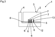
- Figure 2 shows a side view of the sensor system according to Figure 1 .
- the receiving rail 4 has according to Figure 2 on the one hand via a mechanical receptacle for the sensor housing 3 and on the other hand via the flat contact element 5 with which the electrical connection to the sensor housing 3 is established.
- the conductor tracks 6 of the flat contact element 5 can only be contacted, for example, in the region of the rear side of the sensor housing. The remaining area is, for example, insulated.
- the flat contact element 5 is formed by a flexible, that is, flexible conductor foil.
- the flat contact element 5 contains the conductor tracks 6, which are covered on each side with an insulating layer.
- the conductor tracks 6 are formed without insulation only at the points at which the conductor tracks 6 are to be contacted.
- Flat contact element 5 is arranged on the rigid mounting rail 4.
- the contact pins 7 protrude, for example, from the sensor housing 3, so that they can contact the flat contact element 5 as soon as the sensor housing 3 is placed on the flat contact element 5 and fastened on the mounting rail 4.
- the flat contact element 5 is designed for a large number of position locations or slots for the sensor housing 3.
- the sensor housing 3 can be freely arranged at a certain position.
- the conductor tracks 6 are arranged parallel to one another on the flat contact element 5.
- the mounting rail 4 and the sensor housing 3 each have mechanical locking means 8, as a result of which the sensor housing 3 can be snapped into the mounting rail 4, as a result of which the sensor housing 3 is mechanically fixed in the mounting rail 4.
- the mechanical latching means 8 optionally already specify at least one predefined position of the sensor housing 3. Several predefined layers can also be provided, but correct contacting of the contact element 5 is always ensured.
- the latching means 8 or a latching mechanism consists, for example, of latching and spring elements on the sensor housing 3 and on the mounting rail 4, so that the sensor housing 3 can be latched or snapped into the mounting rail 4.
- the two conductor tracks 6 are provided for two bus lines 9.
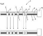
- the flat contact element 5 has at least a third and a fourth interconnect 6, the third interconnect 6 being provided for a ground connection and the fourth interconnect 6 for a supply voltage.
- At least one switching element 12 for the conductor 6 of the supply voltage is provided on the flat contact element 5 for each sensor housing 3, the respective switching element 12 being actuated by an actuating means 13 of the sensor housing 3.
- the sensor housing has five electrical contact pins 7 for the flat contact element, as in FIG Figure 5 shown.
- the flat contact element 5 has five contact surfaces at every possible connection point to sensor housings.
- the five contact pins 7 are two contact pins 7 for the bus lines, one contact pin 7 for the ground connection and two contact pins 7 for the supply lines.
- the interruption and subsequent connection of the supply voltage make it possible, for example, to initialize the sensors 2 in succession. Furthermore, the sensors 2 can thereby be identified, for example, in relation to a higher-level control.
- a higher-level control and evaluation unit 16 knows in which order the sensor housings 3 are arranged.
- the individual control and evaluation units of the sensor housing can interrupt the energy supply locally before each start-up.
- a higher-level control and evaluation unit 16 communicates, for example, with the first sensor 2 or the first sensor housing 3. After an address has been assigned to the first sensor 2 or the first sensor housing 3, the first sensor 2 bridges the energy supply, so that communication takes place with the second sensor 2 and in the same way an assignment or an address assignment for the second sensor 2 takes place.
- the other sensors 2 are initialized accordingly.
- the actuating means 13 or the actuating element is provided on the sensor housing 3.
- the actuating element exerts a force on the switching element 12, which works as a switch.
- the actuating element can consist, for example, of several elements lined up, which are, for example, spring-mounted.
- the respective spring force is greater than the actuating force of the switch. This allows the sensor housing to be attached to the mounting rail without a grid.
- the switching element 12 which is designed, for example, as a normally open contact 15, is closed and the supply voltage is interrupted. The supply voltage is then closed again via an internal contact in the sensor housing 3.
- the switching element 12 can be an electromechanical switch.
- the electromechanical switch can be part of a circuit, for example based on a transistor circuit, in particular with at least one MOSFET transistor.
- the switching element 12 is a normally open contact 15.
- the normally open contact 15 is provided in connection with a transistor in order to interrupt the voltage supply.
- a snap contact is formed as a normally open contact 15 and an additional electronic circuit is provided to interrupt the voltage supply.
- Figure 4 shows the case without sensor.
- the normally open contact S1 is open.
- the voltage U GS -VCC.
- the P-channel MOSFET transistor Q1 switches.
- An optional protective diode Z1 is provided to protect the MOSFET transistor Q1 against overvoltage.
- a sensor 2 with a sensor housing 3 is used.
- the sensor housing 3 is engaged and the normally open contact S1 is closed.
- the voltage U GS 0 volts.
- the contacts or the contact pins 7 are shown schematically.
- the normally open contact 15 is formed, for example, by a metal dome, which functions as a switch.
- the switching elements are formed by metal balls which are held together by elastic elements, can be contacted by a contact pin and can be separated locally by the actuating means.
- the sensors are 2 one-way light barriers.
- a freely definable light grid or a light curtain is formed with any beam spacing, since the sensor housing 3 can be arranged on the mounting rail 4 at any spacing.
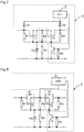
- Figure 7 shows a schematic circuit with two field effect transistors T1 and T2.
- the circuit allows current to flow in both directions.
- the diodes D1 and D2, the resistor R2 and the transistor T3 and the resistor R5 are accommodated in the schematically illustrated sensor housing 3.
- the resistors R1, R2 and R4, the field effect transistors T1 and T2 and the diode D3 are arranged on the mounting rail or the printed circuit board.
- the field effector transistor stage consisting of field effect transistors T1 and T2 on the printed circuit board or a flexible printed circuit board is used for switching the current path.
- the sensor closes the field-effect transistor stage with a low-resistance resistor R5. After addressing, the base connection is switched from T3 to ground, so that the current path is released again.
- Figure 8 shows a further simplified schematic circuit also with two field effect transistors T1 and T2.
- the circuit also allows current to flow in both directions.
- the resistor R2 and the transistor T3 and the resistor R5 are accommodated in the sensor housing 3 shown schematically.
- the resistors R1, R2 and R4, the field effect transistors T1 and T2 and the diodes D1, D2 and D3 are arranged on the mounting rail or the printed circuit board.
- the internal diodes D1 and D2 of the field effect transistors T1 and T2 can be used to supply the sensor 2. This results in even fewer components in the sensor and fewer contact points with the mounting rail.
Landscapes
- Physics & Mathematics (AREA)
- Life Sciences & Earth Sciences (AREA)
- General Life Sciences & Earth Sciences (AREA)
- General Physics & Mathematics (AREA)
- Geophysics (AREA)
- Switches Operated By Changes In Physical Conditions (AREA)
- Push-Button Switches (AREA)
Description
- Die vorliegende Erfindung betrifft ein Sensorsystem gemäß dem Oberbegriff von Anspruch 1.
- Derartige Sensorsysteme sind jeweils aus der
DE 20 2014 102 335 U1 oder derEP 2 208 092 B1 bekannt. Nachteilig bei den genannten Sensorsystemen ist, dass die Sensoren über Leitungen miteinander verbunden sind und Aufwand bei der Inbetriebnahme verursachen. - Die
DE 20 2007 011 016 U1 offenbart einen optischen Sensor zur Erfassung von Objekten in einem Überwachungsbereich, mit wenigstens einem Sendelichtstrahlen emittierenden Sender und wenigstens einem Empfangslichtstrahlen empfangenden Empfänger, wobei der Sender und/oder Empfänger jeweils in einem einstückig ausgebildeten Blendentubus gelagert ist, wobei erste Teile des Blendentubus eine Lichtfalle bilden und weitere Teile zur Lagerung einer Optik und/oder zur Ausbildung einer Blende vorgesehen sind. - Eine Aufgabe der Erfindung besteht darin, ein verbessertes Sensorsystem bereitzustellen, das sehr einfach in Betrieb genommen werden kann und das ohne Kabel auskommt.
- Die Aufgabe wird gemäß Anspruch 1 gelöst durch ein Sensorsystem mit mehreren Sensoren mit jeweils einem Sensorgehäuse, wobei die Sensorgehäuse an einer Aufnahmeschiene befestigbar sind, wobei die Aufnahmeschiene ein flächiges Kontaktelement mit mindestens zwei Leiterbahnen aufweist und die Sensorgehäuse jeweils mindestens zwei Kontaktstifte aufweisen, wobei die Kontaktstifte bei in die Aufnahmeschiene eingesetztem Sensor jeweils mit den Leiterbahnen des flächigen Kontaktelements verbunden sind, wobei das flächige Kontaktelement mindestens eine dritte und eine vierte Leiterbahn aufweist, wobei die dritte Leiterbahn für eine Masseverbindung und die vierte Leiterbahn für eine Versorgungsspannung vorgesehen ist, wobei auf dem flächigen Kontaktelement jeweils für jedes Sensorgehäuse mindestens ein Schaltelement für die Leiterbahn der Versorgungsspannung vorgesehen ist, wobei das jeweilige Schaltelement durch ein Betätigungsmittel des Sensorgehäuses betätigbar ist.
- Die Erfindung ermöglicht eine kabellose Anordnung von Sensorgehäuse mit Sensoren, deren Einbindung über das flächige Kontaktelement und die Aufnahmeschiene erfolgt. Hierbei besitzen die Sensorgehäuse keine Kabelverbindung und keine Stecker-/Buchsenverbindung, sondern elektrische Kontaktstifte, die direkt mit den Leiterbahnen des flächigen Kontaktelements verbunden werden.
- Die Aufnahmeschiene verfügt einerseits über eine mechanische Aufnahme für die Sensorgehäuse und andererseits über das flächige Kontaktelement, mit der die elektrische Verbindung zu den Sensorgehäusen hergestellt wird.
- Die Leiterbahnen des flächigen Kontaktelements sind beispielsweise nur im Bereich der Sensorgehäuserückseite kontaktierbar. Die übrige Fläche ist beispielsweise isoliert ausgeführt. Das flächige Kontaktelement enthält die Leiterbahnen, die auf jeder Seite mit einer Isolierschicht bedeckt sind. Lediglich an den Stellen, an denen die Leiterbahnen kontaktiert werden sollen, sind die Leiterbahnen ohne Isolierung ausgebildet.
- Die Aufnahmeschiene kann beispielsweise aus Kunststoff oder Metall hergestellt sein. Kunststoff hat hier den Vorteil, dass die Aufnahmeschiene selbst isolierend ausgebildet ist. Jedoch können metallische Aufnahmeschienen, beispielsweise aus Aluminium stabiler ausgeführt werden, als Kunststoffschienen. Beispielsweise wird die Aufnahmeschiene im Extrudierverfahren hergestellt. Die Aufnahmeschiene kann optional auch starr ausgeführt sein.
- Die Kontaktstifte stehen beispielsweise aus dem Sensorgehäuse hervor, so dass diese das flächige Kontaktelement kontaktieren können, sobald das Sensorgehäuse auf dem flächigen Kontaktelement aufgesetzt wird und auf der Aufnahmeschiene befestigt wird.
- Das flächige Kontaktelement ist für eine Vielzahl von Positionsplätzen bzw. Steckplätzen für die Sensorgehäuse ausgebildet. Die Sensorgehäuse können dabei frei wählbar an einer bestimmten Position angeordnet werden. Dadurch kann quasi eine frei wählbare Kette von Sensoren gebildet werden.
- Die Leiterbahnen sind dabei parallel nebeneinander auf dem flächigen Kontaktelement angeordnet. Über die Leiterbahnen wird beispielsweise die Energieversorgung und die Signalverbindung mit den Sensorgehäusen und zwischen den Sensorgehäusen durchgeführt.
- In Weiterbildung der Erfindung ist das flächige Kontaktelement eine starre Leiterplatte oder eine Kontaktfolie.
- Beispielsweise ist die Kontaktfolie durch eine flexible, also biegsame Leiterfolie gebildet. Die Kontaktfolie hat den Vorteil, dass diese auf Rollen bevorratet werden kann und einfach in der Aufnahmeschiene angeordnet werden kann. Ein weiterer Vorteil der Kontaktfolie ist, dass diese sehr dünn ausgeführt werden kann.
- Bei der starren Leiterplatte handelt es sich beispielsweise um eine Platine. Diese weist beispielsweise eine oder mehrere Lagen auf. Starre Leiterplatten können sehr robust ausgeführt werden, so dass diese für eine Vielzahl von Kontaktierungsvorgängen geeignet sind.
- In Weiterbildung der Erfindung weisen die Aufnahmeschiene und das Sensorgehäuse jeweils mechanische Rastmittel auf, wodurch die Sensorgehäuse in der Aufnahmeschiene eingerastet werden können, wodurch die Sensorgehäuse in der Aufnahmeschiene mechanisch fixiert sind.
- Dadurch können die Sensorgehäuse ohne zusätzliche verlierbare Befestigungsmittel, wie beispielsweise Schrauben an der Aufnahmeschiene befestigt werden. Die mechanischen Rastmittel geben dabei bereits mindestens eine vordefinierte Lage des Sensorgehäuses vor. Es können auch mehrere vordefinierte Lagen vorgesehen werden, wobei jedoch immer eine richtige Kontaktierung mit dem flächigen Kontaktelement gewährleistet wird.
- Die Sensorgehäuse können dabei auch wieder bei Bedarf entfernt werden. Hierzu werden die mechanischen Rastmittel gelöst und das Sensorgehäuse kann wieder entfernt werden.
- Die Rastmittel bzw. ein Einrastmechanismus besteht beispielsweise aus Rast- und Federelementen am Sensorgehäuse und an der Aufnahmeschiene, so dass das Sensorgehäuse in die Aufnahmeschiene eingerastet bzw. eingeschnappt werden kann. Damit ist eine Fixierung des Sensorgehäuses an der Aufnahmeschiene gewährleistet. Die Fixierung könnte auch magnetisch erfolgen.
- Die Sensorgehäuse können an verschiedenen vordefinierten Positionen einrasten und mit den Leiterbahnen der Aufnahmeschiene kontaktiert werden.
- Beispielsweise kann das Sensorgehäuse in einem modifizierten Kanban System eingesetzt werden. Das Sensorgehäuse wird in der Aufnahmeschiene eingeklickt und kontaktiert. Hierbei kann ein Stromfluss von rechts oder links möglich sein.
- Weiter kann das Sensorgehäuse auch an fahrerlosen Transportfahrzeugen eingesetzt werden. Hierbei können die Sensoren in einer gebogenen Stoßstange eingeklickt werden.
- Weiter kann mit den Sensorgehäusen ein Lichtgitter entlang der Aufnahmeschiene realisiert werden. Dabei werden die Sensorgehäuse in einem bestimmten Raster mit bestimmten Abständen entlang der Aufnahmeschiene angeordnet. Es werden nur die Positionen auf der Aufnahmeschiene bestückt, welche auch benötigt werden.
- Weiter kann das Sensorgehäuse in einem Regalsystem mit einer Pick-to-Light Funktion eingesetzt werden, wobei eine Anzeige ein gültiges Regalfach anzeigt.
- In einer bevorzugten Ausführungsform der Erfindung sind die zwei Leiterbahnen für zwei Busleitungen vorgesehen.
- Bei dem Bus bzw. Bussystem mit zwei Busleitungen kann es sich um ein verfügbares Bussystem nach dem Stand der Technik handeln. Jedoch kann es auch vorgesehen sein, dass ein firmeninternes Bussystem verwendet wird.
- Verfügbare Bussysteme nach dem Stand der Technik sind beispielsweise CAN-Bus, Profibus, Interbus, ASI-Bus, Devicenet oder ähnliche Bussysteme.
- In Weiterbildung der Erfindung weist das flächige Kontaktelement mindestens eine dritte und eine vierte Leiterbahn auf, wobei die dritte Leiterbahn für eine Masseverbindung und die vierte Leiterbahn für eine Versorgungsspannung vorgesehen ist.
- Dadurch wird die Spannungsversorgung bzw. Stromversorgung der Sensorgehäuse getrennt über das flächige Kontaktelement geführt. Dadurch sind alle notwendigen Anschlüsse des Sensorgehäuses über das flächige Kontaktelement geführt. Die Leiterbahnen für die Energieversorgung sind dabei für die maximale Stromaufnahme eines Gesamtsystems ausgelegt. Ggf. sind mehrere Leiterbahnen parallel angeordnet, um die Energieversorgung bereitzustellen.
- Gemäß der Erfindung ist auf dem flächigen Kontaktelement jeweils für jedes Sensorgehäuse mindestens ein Schaltelement für die Leiterbahn der Versorgungsspannung vorgesehen, wobei das jeweilige Schaltelement durch ein Betätigungsmittel des Sensorgehäuses betätigt wird.
- Dadurch ist es möglich, die Versorgungsspannung lokal durch den Sensor bzw. das Sensorgehäuse reversibel für andere nachfolgend angeordnete Sensorgehäuse zu unterbrechen. Diese Leitung wird dann anschließend im Sensorgehäuse geschlossen. Das Sensorgehäuse besitzt hierzu fünf elektrische Kontaktstifte zum flächigen Kontaktelement. Das flächige Kontaktelement weist hierzu an jeder möglichen Verbindungsstelle zu Sensorgehäusen fünf Kontaktflächen auf. Die fünf Kontaktstifte sind zwei Kontaktstifte für die Busleitungen, ein Kontaktstift für die Masseverbindung und zwei Kontaktstifte für die Versorgungsleitungen.
- Durch die Unterbrechung und anschließenden Verbindung der Versorgungspannung können beispielsweise die Sensoren nacheinander initialisiert werden. Weiter können die Sensoren dadurch beispielsweise untereinander erkannt oder gegenüber einer übergeordneten Steuerung identifiziert werden.
- Beispielsweise weiß eine übergeordnete Steuerung dadurch, in welcher Reihenfolge die Sensorgehäuse angeordnet sind. Die einzelnen Steuer- und Auswerteeinheiten der Sensorgehäuse können vor jeder Inbetriebnahme lokal die Energieversorgung unterbrechen. Eine übergeordnete Steuer- und Auswerteeinheit kommuniziert beispielsweise mit dem ersten Sensor bzw. dem ersten Sensorgehäuse. Nachdem eine Adresszuordnung für den ersten Sensor bzw. das erste Sensorgehäuse erfolgt ist, überbrückt der erste Sensor die Energieversorgung, so dass eine Kommunikation mit dem zweiten Sensor erfolgt und auf die gleiche Weise eine Zuordnung bzw. eine Adresszuordnung für den zweiten Sensor erfolgt. Entsprechend werden die übrigen Sensoren initialisiert.
- Eine Adresszuordnung wird dabei somit fortlaufend automatisch vorgenommen. Dazu wird die Versorgungsspannung durch den Sensor bzw. das Sensorgehäuse nach und nach weitergeschaltet. Somit ist bei der Kontaktierung des Sensors die Versorgungsspannung aufzutrennen und nach der Adressierung wieder zu schließen.
- Die Kontaktstifte des Sensorgehäuses sind beispielsweise als Federkontaktstifte ausgebildet. Anstelle der Kontaktstifte kann beispielsweise auch mit Kontaktfedern kontaktiert werden.
- Für die Unterbrechung der Leiterbahn ist an dem Sensorgehäuse das Betätigungsmittel bzw. das Betätigungselement vorgesehen. Durch das Einrasten des Sensorgehäuses in die Aufnahmeschiene übt das Betätigungselement eine Kraft auf das Schaltelement aus, welches als Schalter arbeitet.
- Das Betätigungselement kann beispielsweise aus mehreren aneinandergereihten Elementen bestehen, welche beispielsweise federnd gelagert sind. Die jeweilige Federkraft ist größer als die Betätigungskraft des Schalters. Damit kann das Sensorgehäuse rasterlos auf die Aufnahmeschiene aufgebracht werden.
- Dadurch wird beispielsweise das Schaltelement, welches beispielsweise als Schließerkontakt ausgebildet ist, geschlossen und die Versorgungsspannung unterbrochen. Danach wird die Versorgungsspannung wieder über eine interne Kontaktierung im Sensorgehäuse geschlossen.
- Bei dem Schaltelement 12 kann es sich um einen elektromechanischen Schalter handeln.
- Wird der Sensor von der Aufnahmeschiene getrennt, öffnet sich der Schalter wieder und die Stromleitung ist wieder geschlossen.
- Ist der mögliche Steckplatz nicht bestückt, so ist die Versorgungsspannungsleitung nicht unterbrochen. D.h. die Spannungsversorgung bis zum nächsten Sensorgehäuse ist gewährleistet.
- Nach dem Stecken des Sensorgehäuses wird die Spannungsversorgung unterbrochen und nach einer Adressierung wird die Spannungsversorgung weitergeschaltet.
- Pro Steckplatz wird mindestens ein Schaltelement vorgesehen, auch wenn der Steckplatz nicht durch ein Sensorgehäuse bestückt ist.
- Die Sensorgehäuse können umgesteckt werden oder auch neue Sensorgehäuse hinzugefügt werden.
- Die Spannungseinspeisung auf der Versorgungsspannungsleitung kann an einer beliebigen Stelle erfolgen, so dass der Stromfluss in beiden Richtungen der Versorgungsspannungsleitung möglich ist.
- In Weiterbildung der Erfindung ist das Schaltelement ein Öffnerkontakt oder ein Schließerkontakt.
Der Öffnerkontakt bzw. Schließerkontakt kann beispielsweise als Schnappkontakt ausgeführt sein. - Ein Öffnerkontakt hat den Vorteil, dass damit beim Betätigen die Spannungs- bzw. Energieversorgung direkt unterbrochen werden kann.
- Ein Schließerkontakt kann beispielsweise in Verbindung mit einem Transistor vorgesehen sein, um die Spannungsversorgung zu unterbrechen. Ein Schließerkontakt hat dabei den Vorteil, dass der Schalter an sich einfacher ausgeführt werden kann, da Schließerkontakte einfacher zu realisieren sind.
- Beispielsweise ist ein Schnappkontakt als Schließer ausgebildet und eine zusätzliche Elektronikschaltung ist vorgesehen, um die Spannungsversorgung zu unterbrechen.
- Der Öffnerkontakt bzw. Schließerkontakt ist beispielsweise durch einen Metall-Dom gebildet, welcher als Schalter funktioniert.
- Beispielsweise können die Schaltelemente auch durch Metallkugeln gebildet werden, welche über elastische Elemente zusammengehalten werden, durch einen Kontaktstift kontaktierbar sind und durch das Betätigungsmittel lokal trennbar sind.
- In Weiterbildung der Erfindung ist das Schaltelement mindestens ein Feldeffekttransistor oder eine Feldeffekttransistorstufe.
- Dabei kann der Öffnerkontakt oder der Schließerkontakt durch den mindestens einen Feldeffekttransistor oder die Feldeffekttransistorstufe realisiert sein.
- In dieser Ausführung kann der elektromechanische Schalter Teil einer Schaltung sein, beispielsweise auf Basis einer Transistorschaltung, insbesondere mit mindestens einem Feldeffekttransistor oder MOSFET-Transistor.
- Beispielsweise ist eine Schaltung mit zwei Feldeffekttransistoren vorgesehen. Die Schaltung erlaubt einen Stromfluss in beiden Richtungen. Dabei sind weitere Bauteile, wie Dioden, mindestens ein Widerstand und mindestens ein Transistor im Sensorgehäuse untergebracht. Für das Weiterschalten des Strompfades wird eine Feldeffektortransistorstufe bestehend aus zwei Feldeffekttransistoren auf dem flächigen Kontaktelement bzw. auf der Leiterplatte oder einer Kontaktfolie genutzt. Statt mit einem Schalter schließt der Sensor mit einem niederohmigen Widerstand die Feldeffektortransistorstufe. Nach erfolgter Adressierung wird der Strompfad wieder frei geschaltet.
- Neben Lösungen mit mechanischen Schaltern ist die Lösung mit Feldeffekttransistoren eine Lösung, die keinen mechanischen Schalter benötigt und sehr kostengünstig ist.
- Ein zusätzlicher Vorteil ist, dass für das Weiterschalten der Spannung der vorhandene Feldeffekttransistor auf dem flächigen Kontaktelement genutzt wird und das Durchschalten im Sensor entfällt. Somit wird im Sensor kein Leistungsschaltelement für einen großen Stromfluss mehr benötigt. Ein weiterer Vorteil ist, dass der Stromfluss von beiden Richtungen erfolgen kann.
- Gemäß einer bevorzugten Ausführungsform der Erfindung sind die Sensoren Einweglichtschranken, Reflexionslichtschranken, Lichttaster und/oder Distanzsensoren. Distanzsensoren basieren dabei beispielsweise auf dem Time-of-flight Verfahren, bei dem die Lichtlaufzeit ausgewertet wird. Weiter können Distanzsensoren auch nach dem Prinzip der Triangulation arbeiten.
- Im Falle von Lichtschranken als Sensoren kann dabei beispielsweise ein frei definierbares Lichtgitter bzw. ein Lichtvorhang mit beliebigen Strahlabständen gebildet werden, da die Sensorgehäuse in beliebigen Abständen auf der Aufnahmeschiene angeordnet werden können.
- Auch ist es möglich, unterschiedliche Sensoren an der Aufnahmeschiene anzuordnen. Beispielsweise können Einweglichtschranken, Reflexionslichtschranken, Lichttaster und/oder Distanzsensoren in beliebiger Reihenfolge und Abfolge angeordnet werden, um gezielt bestimmte Anwendungsfälle zu realisieren. Dadurch ist eine speziell anpassbare Anordnung von Sensoren möglich. Die Schiene kann auch nichtlinear ausgeführt werden. Das heißt z.B. gebogen mit einem gewissen Radius.
- In Weiterbildung der Erfindung ist eine zentrale Steuer- und Auswerteeinheit vorgesehen, welche mit den Sensorgehäusen über das flächige Kontaktelement verbunden ist.
- Die Steuer- und Auswerteeinheit wird dann auch wie die Sensorgehäuse über Kontaktstifte mit dem flächigen Kontaktelement verbunden, wobei die Steuer- und Auswerteeinheit ebenfalls über die Aufnahmeschiene befestigt wird.
- In Weiterbildung der Erfindung ist das Sensorgehäuse zweiteilig aufgebaut, wobei ein erstes Teilgehäuse die Sensorelemente aufnimmt und ein zweites Teilgehäuse die Kontaktstifte aufweist, wobei das erste Teilgehäuse und das zweite Teilgehäuse über Steckkontakte miteinander verbunden sind.
- In Weiterbildung der Erfindung können mehrere Aufnahmeschienen mechanisch bzw. mehrere flächige Kontaktelemente elektrisch miteinander verbunden werden. Hierzu ist beispielsweise zwischen flächigen Kontaktelementen ein Kabel mit Steckern verbunden.
- In Weiterbildung weist das flächige Kontaktelement Löcher oder Aussparungen auf, um eine Ausrichtung des Sensorgehäuses relativ zu den Kontaktstellen bzw. dem Schalter zu gewährleisten.
- Die Erfindung wird nachstehend auch hinsichtlich weiterer Vorteile und Merkmale unter Bezugnahme auf die beigefügte Zeichnung anhand von Ausführungsbeispielen erläutert. Die Figuren der Zeichnung zeigen in:
- Figur 1
- ein Sensorsystem;
- Figur 2 und 3
- jeweils eine Seitenansicht eines Sensorsystems;
- Figur 4 und 5
- jeweils ein Schaltelement als Schließerkontakt auf der Kontaktfolie;
- Figur 6
- ein Sensorsystem mit Einweglichtschranken;
- Figur 7 und 8
- eine schematische Schaltung mit zwei Feldeffekttransistoren.
- In den nachfolgenden Figuren sind identische Teile mit identischen Bezugszeichen versehen.
Figur 1 zeigt ein Sensorsystem 1 mit mehreren Sensoren 2 mit jeweils einem Sensorgehäuse 3, dadurch gekennzeichnet, dass die Sensorgehäuse 3 an einer Aufnahmeschiene 4 befestigbar sind, wobei die Aufnahmeschiene 4 ein flächiges Kontaktelement 5 mit mindestens zwei Leiterbahnen 6 aufweist und die Sensorgehäuse 3 jeweils mindestens zwei Kontaktstifte 7 aufweisen, wobei die Kontaktstifte 7 bei in die Aufnahmeschiene 4 eingesetztem Sensor 2 jeweils mit den Leiterbahnen 6 des flächigen Kontaktelements 5 verbunden sind. Die Aufnahmeschiene ist optional starr ausgeführt. - Gemäß den Figuren ist das flächige Kontaktelement 5 eine starre Leiterplatte 17 oder eine Kontaktfolie 18, insbesondere eine flexible Kontaktfolie.
- Auch ist es möglich, gemäß
Figur 1 unterschiedliche Sensoren 2 an der Aufnahmeschiene 4 anzuordnen. Beispielsweise können Einweglichtschranken, Reflexionslichtschranken, Lichttaster und/oder Distanzsensoren in beliebiger Reihenfolge und Abfolge angeordnet werden. - Gemäß
Figur 1 ist eine zentrale Steuer- und Auswerteeinheit 16 vorgesehen, welche mit den Sensorgehäusen 3 über das flächige Kontaktelement 5 verbunden ist. - Die Steuer- und Auswerteeinheit 16 wird beispielsweise auch wie die Sensorgehäuse 3 über Kontaktstifte 7 mit dem flächigen Kontaktelement 5 verbunden, wobei die Steuer- und Auswerteeinheit 16 ebenfalls über die Aufnahmeschiene 4 befestigt wird.
-
Figur 2 zeigt eine Seitenansicht auf das Sensorsystem gemäßFigur 1 . - Die Aufnahmeschiene 4 verfügt gemäß
Figur 2 einerseits über eine mechanische Aufnahme für die Sensorgehäuse 3 und andererseits über das flächige Kontaktelement 5, mit der die elektrische Verbindung zu den Sensorgehäusen 3 hergestellt wird. - Die Leiterbahnen 6 des flächigen Kontaktelements 5 sind beispielsweise nur im Bereich der Sensorgehäuserückseite kontaktierbar. Die übrige Fläche ist beispielsweise isoliert ausgeführt. Beispielsweise ist das flächige Kontaktelement 5 durch eine flexible, also biegsame Leiterfolie gebildet. Das flächige Kontaktelement 5 enthält die Leiterbahnen 6, die auf jeder Seite mit einer Isolierschicht bedeckt sind. Lediglich an den Stellen, an denen die Leiterbahnen 6 kontaktiert werden sollen, sind die Leiterbahnen 6 ohne Isolierung ausgebildet. An der starren Aufnahmeschiene 4 ist flächige Kontaktelement 5 angeordnet.
- Die Kontaktstifte 7 stehen beispielsweise aus dem Sensorgehäuse 3 hervor, so dass diese das flächige Kontaktelement 5 kontaktieren können, sobald das Sensorgehäuse 3 auf das flächige Kontaktelement 5 aufgesetzt wird und auf der Aufnahmeschiene 4 befestigt wird.
- Das flächige Kontaktelement 5 ist für eine Vielzahl von Positionsplätzen bzw. Steckplätzen für die Sensorgehäuse 3 ausgebildet. Die Sensorgehäuse 3 können dabei frei wählbar an einer bestimmten Position angeordnet werden. Die Leiterbahnen 6 sind dabei parallel nebeneinander auf dem flächigen Kontaktelement 5 angeordnet.
- Gemäß
Figur 2 weisen die Aufnahmeschiene 4 und das Sensorgehäuse 3 jeweils mechanische Rastmittel 8 auf, wodurch die Sensorgehäuse 3 in der Aufnahmeschiene 4 eingerastet werden können, wodurch die Sensorgehäuse 3 in der Aufnahmeschiene 4 mechanisch fixiert sind. - Die mechanischen Rastmittel 8 geben dabei bereits optional mindestens eine vordefinierte Lage des Sensorgehäuses 3 vor. Es können auch mehrere vordefinierte Lagen vorgesehen werden, wobei jedoch immer eine richtige Kontaktierung des Kontaktelements 5 gewährleistet wird.
- Die Rastmittel 8 bzw. ein Einrastmechanismus besteht beispielsweise aus Rast- und Federelementen am Sensorgehäuse 3 und an der Aufnahmeschiene 4, so dass das Sensorgehäuse 3 in die Aufnahmeschiene 4 eingerastet bzw. eingeschnappt werden kann.
- Gemäß
Figur 2 sind die zwei Leiterbahnen 6 für zwei Busleitungen 9 vorgesehen. - Gemäß
Figur 3 weist das flächige Kontaktelement 5 mindestens eine dritte und eine vierte Leiterbahn 6 auf, wobei die dritte Leiterbahn 6 für eine Masseverbindung und die vierte Leiterbahn 6 für eine Versorgungsspannung vorgesehen ist. - Gemäß
Figur 3 ist auf dem flächigen Kontaktelement 5 jeweils für jedes Sensorgehäuse 3 mindestens ein Schaltelement 12 für die Leiterbahn 6 der Versorgungsspannung vorgesehen, wobei das jeweilige Schaltelement 12 durch ein Betätigungsmittel 13 des Sensorgehäuses 3 betätigt wird. - Dadurch ist es wie in
Figur 4 und 5 dargestellt möglich, die Versorgungsspannung lokal durch den Sensor 2 bzw. das Sensorgehäuse reversibel für andere nachfolgend angeordnete Sensorgehäuse zu unterbrechen. Diese Leitung wird dann anschließend im Sensorgehäuse geschlossen. Das Sensorgehäuse besitzt hierzu fünf elektrische Kontaktstifte 7 zum flächigen Kontaktelement, wie inFigur 5 dargestellt. Das flächige Kontaktelement 5 weist hierzu an jeder möglichen Verbindungsstelle zu Sensorgehäusen fünf Kontaktflächen auf. Die fünf Kontaktstifte 7 sind zwei Kontaktstifte 7 für die Busleitungen, ein Kontaktstift 7 für die Masseverbindung und zwei Kontaktstifte 7 für die Versorgungsleitungen. - Durch die Unterbrechung und anschließende Verbindung der Versorgungspannung können beispielsweise die Sensoren 2 nacheinander initialisiert werden. Weiter können die Sensoren 2 dadurch beispielsweise gegenüber einer übergeordneten Steuerung identifiziert werden.
- Gemäß
Figur 1 weiß eine übergeordnete Steuer- und Auswerteeinheit 16 dadurch, in welcher Reihenfolge die Sensorgehäuse 3 angeordnet sind. Die einzelnen Steuer- und Auswerteeinheiten der Sensorgehäuse können vor jeder Inbetriebnahme lokal die Energieversorgung unterbrechen. Eine übergeordnete Steuer- und Auswerteeinheit 16 kommuniziert beispielsweise mit dem ersten Sensor 2 bzw. dem ersten Sensorgehäuse 3. Nachdem eine Adresszuordnung für den ersten Sensor 2 bzw. das erste Sensorgehäuse 3 erfolgt ist, überbrückt der erste Sensor 2 die Energieversorgung, so dass eine Kommunikation mit dem zweiten Sensor 2 erfolgt und auf die gleiche Weise eine Zuordnung bzw. eine Adresszuordnung für den zweiten Sensor 2 erfolgt. Entsprechend werden die übrigen Sensoren 2 initialisiert. - Für die Unterbrechung der Leiterbahn 6 ist an dem Sensorgehäuse 3 das Betätigungsmittel 13 bzw. das Betätigungselement vorgesehen. Durch das Einrasten des Sensorgehäuses 3 in die Aufnahmeschiene 4 übt das Betätigungselement eine Kraft auf das Schaltelement 12 aus, welches als Schalter arbeitet.
- Das Betätigungselement kann beispielsweise aus mehreren aneinandergereihten Elementen bestehen, welche beispielsweise federnd gelagert sind. Die jeweilige Federkraft ist größer als die Betätigungskraft des Schalters. Damit kann das Sensorgehäuse rasterlos auf die Aufnahmeschiene aufgebracht werden.
- Dadurch wird beispielsweise das Schaltelement 12, welches beispielsweise als Schließerkontakt 15 ausgebildet ist, geschlossen und die Versorgungsspannung unterbrochen. Danach wird die Versorgungsspannung wieder über eine interne Kontaktierung im Sensorgehäuse 3 geschlossen.
- Bei dem Schaltelement 12 kann es sich um einen elektromechanischen Schalter handeln.
- In einer anderen Ausführung kann der elektromechanische Schalter Teil einer Schaltung sein, beispielsweise auf Basis einer Transistorschaltung, insbesondere mit mindestens einem MOSFET-Transistor.
- Wird der Sensor 2 von der Aufnahmeschiene 4 getrennt, öffnet sich der Schalter wieder und die Stromleitung ist wieder geschlossen.
- Gemäß
Figur 4 ist das Schaltelement 12 ein Schließerkontakt 15. - Der Schließerkontakt 15 ist in Verbindung mit einem Transistor vorgesehen, um die Spannungsversorgung zu unterbrechen.
- Gemäß
Figur 4 ist ein Schnappkontakt als Schließerkontakt 15 ausgebildet und eine zusätzliche Elektronikschaltung ist vorgesehen, um die Spannungsversorgung zu unterbrechen. -
Figur 4 zeigt den Fall ohne Sensor. Der Schließerkontakt S1 ist offen. Die Spannung UGS = -VCC. Der P-Channel MOSFET Transistor Q1 schaltet. Es ist eine optionale Schutzdiode Z1 zum Schutz des MOSFET Transistor Q1 vor Überspannung vorgesehen. - Gemäß
Figur 5 ist ein Sensor 2 mit einem Sensorgehäuse 3 eingesetzt. Das Sensorgehäuse 3 ist eingerastet und der Schließerkontakt S1 geschlossen. Die Spannung UGS = 0 Volt. Die Kontaktierungen bzw. die Kontaktstifte 7 sind schematisch eingezeichnet. - Der Schließerkontakt 15 ist beispielsweise durch einen Metall-Dom gebildet, welcher als Schalter funktioniert.
- Gemäß einem nicht dargestellten Ausführungsbeispiel sind die Schaltelemente durch Metallkugeln gebildet, welche über elastische Elemente zusammengehalten werden, durch einen Kontaktstift kontaktierbar sind und durch das Betätigungsmittel lokal trennbar sind.
- Gemäß
Figur 6 sind die Sensoren 2 Einweglichtschranken. Im Falle von Lichtschranken als Sensoren 2 wird dabei gemäßFigur 6 ein frei definierbares Lichtgitter bzw. ein Lichtvorhang mit beliebigen Strahlabständen gebildet, da die Sensorgehäuse 3 in beliebigen Abständen auf der Aufnahmeschiene 4 angeordnet werden können. - Gemäß einem nicht dargestellten Ausführungsbeispiel ist das Sensorgehäuse zweiteilig aufgebaut, wobei ein erstes Teilgehäuse die Sensorelemente aufnimmt und ein zweites Teilgehäuse die Kontaktstifte aufweist, wobei das erste Teilgehäuse und das zweite Teilgehäuse über Steckkontakte miteinander verbunden sind.
-
Figur 7 zeigt eine schematische Schaltung mit zwei Feldeffekttransistoren T1 und T2. Die Schaltung erlaubt einen Stromfluss in beiden Richtungen. Dabei sind die Dioden D1 und D2, der Widerstand R2 und der Transistor T3 sowie der Widerstand R5 im schematisch dargestellten Sensorgehäuse 3 untergebracht. Die Widerstände R1, R2 und R4, die Feldeffekttransistorren T1 und T2 sowie die Diode D3 sind auf der Aufnahmeschiene bzw. der Leiterplatte angeordnet. Für das Weiterschalten des Strompfades wird die Feldeffektortransistorstufe bestehend aus den Feldeffekttransistoren T1 und T2 auf der Leiterplatte oder einer flexiblen Leiterplatte genutzt. Statt mit einem Schalter schließt der Sensor mit einem niederohmigen Widerstand R5 die Feldeffektortransistorstufe. Nach erfolgter Adressierung wird der Basisanschluss von T3 auf Masse geschaltet, damit wird der Strompfad wieder frei geschaltet. -
Figur 8 zeigt eine weiter vereinfachte schematische Schaltung ebenfalls mit zwei Feldeffekttransistoren T1 und T2. Die Schaltung erlaubt ebenfalls einen Stromfluss in beiden Richtungen. Dabei sind der Widerstand R2 und der Transistor T3 sowie der Widerstand R5 im schematisch dargestellten Sensorgehäuse 3 untergebracht. Die Widerstände R1, R2 und R4, die Feldeffekttransistorren T1 und T2 sowie die Dioden D1, D2 und D3 sind auf der Aufnahmeschiene bzw. der Leiterplatte angeordnet. Die internen Dioden D1 und D2 der Feldeffekttransistoren T1 und T2 können zur Versorgung des Sensors 2 mitgenutzt werden. Damit ergeben sich noch weniger Bauelemente im Sensor und weniger Kontaktpunkte zur Aufnahmeschiene. -
- 1 Sensorsystem
- 2 Sensor
- 3 Sensorgehäuse
- 4 Aufnahmeschiene
- 5 flächiges Kontaktelement
- 6 Leiterbahn
- 7 Kontaktstifte
- 8 mechanische Rastmittel
- 9 Busleitungen
- 10 Masseleitung
- 11 Versorgungsspannungsleitung
- 12 Schaltelement
- 13 Betätigungsmittel
- 15 Schließerkontakt
- 16 Steuer- und Auswerteeinheit
- 17 starre Leiterplatte
- 18 Kontaktfolie
- R1, R2, R3, R4, R5 Widerstände
- D1, D2, D3 Dioden
- T1, T2 Feldeffekttransistoren
- T3 Transistor
Claims (9)
- Sensorsystem (1) mit mehreren Sensoren (2) mit jeweils einem Sensorgehäuse (3), wobei
die Sensorgehäuse (3) an einer Aufnahmeschiene (4) befestigbar sind,
wobei die Aufnahmeschiene (4) ein flächiges Kontaktelement (5) mit mindestens zwei Leiterbahnen (6) aufweist und die Sensorgehäuse (3) jeweils mindestens zwei Kontaktstifte (7) aufweisen,
wobei die Kontaktstifte (7) bei in die Aufnahmeschiene (4) eingesetztem Sensor (2) jeweils mit den Leiterbahnen (6) des flächigen Kontaktelements (5) verbunden sind, dadurch gekennzeichnet, dass das flächige Kontaktelement (5) mindestens eine dritte und eine vierte Leiterbahn (6) aufweist, wobei die dritte Leiterbahn (6) für eine Masseverbindung und die vierte Leiterbahn (6) für eine Versorgungsspannung vorgesehen ist, wobei auf dem flächigen Kontaktelement (5) jeweils für jedes Sensorgehäuse (3) mindestens ein Schaltelement (12) für die Leiterbahn (6) der Versorgungsspannung vorgesehen ist, wobei das jeweilige Schaltelement (12) durch ein Betätigungsmittel (13) des Sensorgehäuses (3) betätigbar ist. - Sensorsystem nach Anspruch 1, dadurch gekennzeichnet, dass das flächige Kontaktelement eine starre Leiterplatte (17) oder eine Kontaktfolie (18) ist.
- Sensorsystem nach mindestens einem der vorhergehenden Ansprüche, dadurch gekennzeichnet, dass die Aufnahmeschiene (4) und die Sensorgehäuse (3) jeweils mechanische Rastmittel (8) aufweisen, wodurch die Sensorgehäuse (3) in der Aufnahmeschiene (4) eingerastet werden können, wodurch die Sensorgehäuse (3) in der Aufnahmeschiene (4) mechanisch fixiert sind.
- Sensorsystem nach mindestens einem der vorhergehenden Ansprüche, dadurch gekennzeichnet, dass die zwei Leiterbahnen (6) für zwei Busleitungen vorgesehen sind.
- Sensorsystem nach mindestens einem der vorhergehenden Ansprüche, dadurch gekennzeichnet, dass das Schaltelement (12) mindestens ein Öffnerkontakt oder mindestens ein Schließerkontakt (15) ist.
- Sensorsystem nach mindestens einem der vorhergehenden Ansprüche, dadurch gekennzeichnet, dass das Schaltelement (12) mindestens ein Feldeffekttransistor oder eine Feldeffekttransistorstufe ist.
- Sensorsystem nach mindestens einem der vorhergehenden Ansprüche, dadurch gekennzeichnet, dass die Sensoren (2) Einweglichtschranken, Reflexionslichtschranken, Lichttaster und/oder Distanzsensoren sind.
- Sensorsystem nach mindestens einem der vorhergehenden Ansprüche, dadurch gekennzeichnet, dass eine zentrale Steuer- und Auswerteeinheit (16) vorgesehen ist, welche mit den Sensorgehäusen (3) über das flächige Kontaktelement (5) verbunden ist.
- Sensorsystem nach mindestens einem der vorhergehenden Ansprüche, dadurch gekennzeichnet, dass das Sensorgehäuse (3) zweiteilig aufgebaut ist, wobei ein erstes Teilgehäuse die Sensorelemente aufnimmt und ein zweites Teilgehäuse die Kontaktstifte aufweist, wobei das erste Teilgehäuse und das zweite Teilgehäuse über Steckkontakte miteinander verbunden sind.
Applications Claiming Priority (1)
| Application Number | Priority Date | Filing Date | Title |
|---|---|---|---|
| EP17185957.2A EP3441796B1 (de) | 2017-08-11 | 2017-08-11 | Sensorsystem |
Publications (2)
| Publication Number | Publication Date |
|---|---|
| EP3441797A1 EP3441797A1 (de) | 2019-02-13 |
| EP3441797B1 true EP3441797B1 (de) | 2020-04-15 |
Family
ID=59702531
Family Applications (2)
| Application Number | Title | Priority Date | Filing Date |
|---|---|---|---|
| EP17185957.2A Active EP3441796B1 (de) | 2017-08-11 | 2017-08-11 | Sensorsystem |
| EP18186409.1A Active EP3441797B1 (de) | 2017-08-11 | 2018-07-30 | Sensorsystem |
Family Applications Before (1)
| Application Number | Title | Priority Date | Filing Date |
|---|---|---|---|
| EP17185957.2A Active EP3441796B1 (de) | 2017-08-11 | 2017-08-11 | Sensorsystem |
Country Status (1)
| Country | Link |
|---|---|
| EP (2) | EP3441796B1 (de) |
Family Cites Families (5)
| Publication number | Priority date | Publication date | Assignee | Title |
|---|---|---|---|---|
| DE102005046478B4 (de) * | 2004-09-30 | 2019-03-14 | Omron Corp. | Photoelektrischer Mehrstrahl-Sensor |
| EP2157413A4 (de) * | 2007-06-08 | 2013-06-26 | Panasonic Corp | Infrarotstrahlendetektor |
| DE202007011016U1 (de) * | 2007-08-07 | 2007-10-31 | Leuze Electronic Gmbh & Co Kg | Optischer Sensor |
| EP2208092B2 (de) | 2007-11-07 | 2021-09-15 | Cedes AG | System zur feststellung eines objekts in einer überwachungsfläche |
| DE202014102335U1 (de) | 2014-05-19 | 2015-08-24 | Sick Ag | Sensorsystem |
-
2017
- 2017-08-11 EP EP17185957.2A patent/EP3441796B1/de active Active
-
2018
- 2018-07-30 EP EP18186409.1A patent/EP3441797B1/de active Active
Non-Patent Citations (1)
| Title |
|---|
| None * |
Also Published As
| Publication number | Publication date |
|---|---|
| EP3441797A1 (de) | 2019-02-13 |
| EP3441796A1 (de) | 2019-02-13 |
| EP3441796B1 (de) | 2021-04-21 |
Similar Documents
| Publication | Publication Date | Title |
|---|---|---|
| EP0181534B1 (de) | Einrichtung für ein Kraftfahrzeug | |
| DE4440102C1 (de) | Modulare Steuerungsanlage mit integriertem Feldbusanschluß | |
| DE2414566C2 (de) | Elektrisches Automatiksystem | |
| DE2822245A1 (de) | Verfahren zur herstellung elektrisch leitender verbindungen zwischen gedruckten rueckwandverdrahtungen von leiterplatten und federleisten sowie fuer dieses verfahren geeignete federleiste | |
| WO2008135183A1 (de) | Einrichtung zur überprüfung der befestigung einer leiterbahnplatte an einem träger | |
| DE3740290C2 (de) | Vorrichtung zum Steuern und/oder Regeln von Prozessen | |
| EP2745179B1 (de) | Basiselement zur aufnahme eines überspannungsschutzmoduls und modulares bussystem | |
| EP2843447B1 (de) | Lichtgitter | |
| EP3510676B1 (de) | Überspannungsschutzmodul für einen modularen steckverbinder | |
| DE4422434C1 (de) | Zentralelektrik | |
| EP3441796B1 (de) | Sensorsystem | |
| AT398136B (de) | Vorrichtung zur funktionsüberwachung von überspannungsableitern | |
| DE19821302A1 (de) | Passiv-Infrarot-Bewegungsmelder | |
| WO2000002289A1 (de) | Leitungsverteiler für fernmelde- und sicherheitstechnische anlagen | |
| EP2309238A2 (de) | Heizkostenverteiler | |
| DE202014102335U1 (de) | Sensorsystem | |
| EP3738175A1 (de) | Steckverbinderanordnung | |
| EP2195760B1 (de) | Schutzanordnung und herstellungsverfahren für eine schutzanordnung | |
| EP3859909B1 (de) | Abgriff einer linearen stromverteileranordnung mit einer leiterplatte | |
| DE102016124503B4 (de) | Bedienvorrichtung für ein Kraftfahrzeug mit einer konfigurierbaren Leiterplatte | |
| DE102017203142B4 (de) | Verkettungsmodul | |
| EP3537856A2 (de) | Leiterplattenanordnung mit abstandsbolzen zur datenübertragung zwischen einzelnen leiterplatten | |
| DE2041805A1 (de) | Deckplatte fuer Gehaeuse mit einschiebbaren Leiterplatten | |
| EP3214415B1 (de) | Ein einen mikroprozessor umfassender sensor sowie verfahren zum bereitstellen und einspeisen eines sensorsignals in einen installationsbus einer gebäudeautomatisierungseinrichtung | |
| DE102022113433A1 (de) | Kontaktstecker und Set aus einer elektrischen Anschlussklemme und einem Kontaktstecker |
Legal Events
| Date | Code | Title | Description |
|---|---|---|---|
| PUAI | Public reference made under article 153(3) epc to a published international application that has entered the european phase |
Free format text: ORIGINAL CODE: 0009012 |
|
| STAA | Information on the status of an ep patent application or granted ep patent |
Free format text: STATUS: THE APPLICATION HAS BEEN PUBLISHED |
|
| AK | Designated contracting states |
Kind code of ref document: A1 Designated state(s): AL AT BE BG CH CY CZ DE DK EE ES FI FR GB GR HR HU IE IS IT LI LT LU LV MC MK MT NL NO PL PT RO RS SE SI SK SM TR |
|
| AX | Request for extension of the european patent |
Extension state: BA ME |
|
| STAA | Information on the status of an ep patent application or granted ep patent |
Free format text: STATUS: REQUEST FOR EXAMINATION WAS MADE |
|
| 17P | Request for examination filed |
Effective date: 20190412 |
|
| RBV | Designated contracting states (corrected) |
Designated state(s): AL AT BE BG CH CY CZ DE DK EE ES FI FR GB GR HR HU IE IS IT LI LT LU LV MC MK MT NL NO PL PT RO RS SE SI SK SM TR |
|
| STAA | Information on the status of an ep patent application or granted ep patent |
Free format text: STATUS: EXAMINATION IS IN PROGRESS |
|
| 17Q | First examination report despatched |
Effective date: 20190614 |
|
| GRAP | Despatch of communication of intention to grant a patent |
Free format text: ORIGINAL CODE: EPIDOSNIGR1 |
|
| STAA | Information on the status of an ep patent application or granted ep patent |
Free format text: STATUS: GRANT OF PATENT IS INTENDED |
|
| GRAJ | Information related to disapproval of communication of intention to grant by the applicant or resumption of examination proceedings by the epo deleted |
Free format text: ORIGINAL CODE: EPIDOSDIGR1 |
|
| STAA | Information on the status of an ep patent application or granted ep patent |
Free format text: STATUS: EXAMINATION IS IN PROGRESS |
|
| INTG | Intention to grant announced |
Effective date: 20191113 |
|
| RIN1 | Information on inventor provided before grant (corrected) |
Inventor name: KIENZLER, STEFAN Inventor name: KRIEG, MATTHIAS Inventor name: ALLGEIER, SIMON Inventor name: BUERGER, JUERGEN Inventor name: SCHWIDERSKI, FRANK Inventor name: EBLE, JOHANNES Inventor name: REICHENBACH, HANS-PETER Inventor name: JAEGER, DR. THOMAS |
|
| INTC | Intention to grant announced (deleted) | ||
| GRAP | Despatch of communication of intention to grant a patent |
Free format text: ORIGINAL CODE: EPIDOSNIGR1 |
|
| STAA | Information on the status of an ep patent application or granted ep patent |
Free format text: STATUS: GRANT OF PATENT IS INTENDED |
|
| INTG | Intention to grant announced |
Effective date: 20200109 |
|
| RAP1 | Party data changed (applicant data changed or rights of an application transferred) |
Owner name: SICK AG |
|
| GRAS | Grant fee paid |
Free format text: ORIGINAL CODE: EPIDOSNIGR3 |
|
| GRAA | (expected) grant |
Free format text: ORIGINAL CODE: 0009210 |
|
| STAA | Information on the status of an ep patent application or granted ep patent |
Free format text: STATUS: THE PATENT HAS BEEN GRANTED |
|
| AK | Designated contracting states |
Kind code of ref document: B1 Designated state(s): AL AT BE BG CH CY CZ DE DK EE ES FI FR GB GR HR HU IE IS IT LI LT LU LV MC MK MT NL NO PL PT RO RS SE SI SK SM TR |
|
| REG | Reference to a national code |
Ref country code: CH Ref legal event code: EP |
|
| REG | Reference to a national code |
Ref country code: DE Ref legal event code: R096 Ref document number: 502018001194 Country of ref document: DE |
|
| REG | Reference to a national code |
Ref country code: IE Ref legal event code: FG4D Free format text: LANGUAGE OF EP DOCUMENT: GERMAN |
|
| REG | Reference to a national code |
Ref country code: AT Ref legal event code: REF Ref document number: 1257982 Country of ref document: AT Kind code of ref document: T Effective date: 20200515 |
|
| REG | Reference to a national code |
Ref country code: NL Ref legal event code: MP Effective date: 20200415 |
|
| REG | Reference to a national code |
Ref country code: LT Ref legal event code: MG4D |
|
| PG25 | Lapsed in a contracting state [announced via postgrant information from national office to epo] |
Ref country code: NL Free format text: LAPSE BECAUSE OF FAILURE TO SUBMIT A TRANSLATION OF THE DESCRIPTION OR TO PAY THE FEE WITHIN THE PRESCRIBED TIME-LIMIT Effective date: 20200415 Ref country code: LT Free format text: LAPSE BECAUSE OF FAILURE TO SUBMIT A TRANSLATION OF THE DESCRIPTION OR TO PAY THE FEE WITHIN THE PRESCRIBED TIME-LIMIT Effective date: 20200415 Ref country code: GR Free format text: LAPSE BECAUSE OF FAILURE TO SUBMIT A TRANSLATION OF THE DESCRIPTION OR TO PAY THE FEE WITHIN THE PRESCRIBED TIME-LIMIT Effective date: 20200716 Ref country code: NO Free format text: LAPSE BECAUSE OF FAILURE TO SUBMIT A TRANSLATION OF THE DESCRIPTION OR TO PAY THE FEE WITHIN THE PRESCRIBED TIME-LIMIT Effective date: 20200715 Ref country code: FI Free format text: LAPSE BECAUSE OF FAILURE TO SUBMIT A TRANSLATION OF THE DESCRIPTION OR TO PAY THE FEE WITHIN THE PRESCRIBED TIME-LIMIT Effective date: 20200415 Ref country code: SE Free format text: LAPSE BECAUSE OF FAILURE TO SUBMIT A TRANSLATION OF THE DESCRIPTION OR TO PAY THE FEE WITHIN THE PRESCRIBED TIME-LIMIT Effective date: 20200415 Ref country code: IS Free format text: LAPSE BECAUSE OF FAILURE TO SUBMIT A TRANSLATION OF THE DESCRIPTION OR TO PAY THE FEE WITHIN THE PRESCRIBED TIME-LIMIT Effective date: 20200815 Ref country code: PT Free format text: LAPSE BECAUSE OF FAILURE TO SUBMIT A TRANSLATION OF THE DESCRIPTION OR TO PAY THE FEE WITHIN THE PRESCRIBED TIME-LIMIT Effective date: 20200817 |
|
| PG25 | Lapsed in a contracting state [announced via postgrant information from national office to epo] |
Ref country code: LV Free format text: LAPSE BECAUSE OF FAILURE TO SUBMIT A TRANSLATION OF THE DESCRIPTION OR TO PAY THE FEE WITHIN THE PRESCRIBED TIME-LIMIT Effective date: 20200415 Ref country code: RS Free format text: LAPSE BECAUSE OF FAILURE TO SUBMIT A TRANSLATION OF THE DESCRIPTION OR TO PAY THE FEE WITHIN THE PRESCRIBED TIME-LIMIT Effective date: 20200415 Ref country code: HR Free format text: LAPSE BECAUSE OF FAILURE TO SUBMIT A TRANSLATION OF THE DESCRIPTION OR TO PAY THE FEE WITHIN THE PRESCRIBED TIME-LIMIT Effective date: 20200415 Ref country code: BG Free format text: LAPSE BECAUSE OF FAILURE TO SUBMIT A TRANSLATION OF THE DESCRIPTION OR TO PAY THE FEE WITHIN THE PRESCRIBED TIME-LIMIT Effective date: 20200715 |
|
| PG25 | Lapsed in a contracting state [announced via postgrant information from national office to epo] |
Ref country code: AL Free format text: LAPSE BECAUSE OF FAILURE TO SUBMIT A TRANSLATION OF THE DESCRIPTION OR TO PAY THE FEE WITHIN THE PRESCRIBED TIME-LIMIT Effective date: 20200415 |
|
| REG | Reference to a national code |
Ref country code: DE Ref legal event code: R097 Ref document number: 502018001194 Country of ref document: DE |
|
| PG25 | Lapsed in a contracting state [announced via postgrant information from national office to epo] |
Ref country code: CZ Free format text: LAPSE BECAUSE OF FAILURE TO SUBMIT A TRANSLATION OF THE DESCRIPTION OR TO PAY THE FEE WITHIN THE PRESCRIBED TIME-LIMIT Effective date: 20200415 Ref country code: IT Free format text: LAPSE BECAUSE OF FAILURE TO SUBMIT A TRANSLATION OF THE DESCRIPTION OR TO PAY THE FEE WITHIN THE PRESCRIBED TIME-LIMIT Effective date: 20200415 Ref country code: EE Free format text: LAPSE BECAUSE OF FAILURE TO SUBMIT A TRANSLATION OF THE DESCRIPTION OR TO PAY THE FEE WITHIN THE PRESCRIBED TIME-LIMIT Effective date: 20200415 Ref country code: SM Free format text: LAPSE BECAUSE OF FAILURE TO SUBMIT A TRANSLATION OF THE DESCRIPTION OR TO PAY THE FEE WITHIN THE PRESCRIBED TIME-LIMIT Effective date: 20200415 Ref country code: DK Free format text: LAPSE BECAUSE OF FAILURE TO SUBMIT A TRANSLATION OF THE DESCRIPTION OR TO PAY THE FEE WITHIN THE PRESCRIBED TIME-LIMIT Effective date: 20200415 Ref country code: ES Free format text: LAPSE BECAUSE OF FAILURE TO SUBMIT A TRANSLATION OF THE DESCRIPTION OR TO PAY THE FEE WITHIN THE PRESCRIBED TIME-LIMIT Effective date: 20200415 Ref country code: RO Free format text: LAPSE BECAUSE OF FAILURE TO SUBMIT A TRANSLATION OF THE DESCRIPTION OR TO PAY THE FEE WITHIN THE PRESCRIBED TIME-LIMIT Effective date: 20200415 |
|
| PLBE | No opposition filed within time limit |
Free format text: ORIGINAL CODE: 0009261 |
|
| STAA | Information on the status of an ep patent application or granted ep patent |
Free format text: STATUS: NO OPPOSITION FILED WITHIN TIME LIMIT |
|
| PG25 | Lapsed in a contracting state [announced via postgrant information from national office to epo] |
Ref country code: SK Free format text: LAPSE BECAUSE OF FAILURE TO SUBMIT A TRANSLATION OF THE DESCRIPTION OR TO PAY THE FEE WITHIN THE PRESCRIBED TIME-LIMIT Effective date: 20200415 Ref country code: PL Free format text: LAPSE BECAUSE OF FAILURE TO SUBMIT A TRANSLATION OF THE DESCRIPTION OR TO PAY THE FEE WITHIN THE PRESCRIBED TIME-LIMIT Effective date: 20200415 Ref country code: MC Free format text: LAPSE BECAUSE OF FAILURE TO SUBMIT A TRANSLATION OF THE DESCRIPTION OR TO PAY THE FEE WITHIN THE PRESCRIBED TIME-LIMIT Effective date: 20200415 |
|
| 26N | No opposition filed |
Effective date: 20210118 |
|
| REG | Reference to a national code |
Ref country code: BE Ref legal event code: MM Effective date: 20200731 |
|
| PG25 | Lapsed in a contracting state [announced via postgrant information from national office to epo] |
Ref country code: LU Free format text: LAPSE BECAUSE OF NON-PAYMENT OF DUE FEES Effective date: 20200730 |
|
| PG25 | Lapsed in a contracting state [announced via postgrant information from national office to epo] |
Ref country code: SI Free format text: LAPSE BECAUSE OF FAILURE TO SUBMIT A TRANSLATION OF THE DESCRIPTION OR TO PAY THE FEE WITHIN THE PRESCRIBED TIME-LIMIT Effective date: 20200415 Ref country code: BE Free format text: LAPSE BECAUSE OF NON-PAYMENT OF DUE FEES Effective date: 20200731 |
|
| PG25 | Lapsed in a contracting state [announced via postgrant information from national office to epo] |
Ref country code: IE Free format text: LAPSE BECAUSE OF NON-PAYMENT OF DUE FEES Effective date: 20200730 |
|
| PG25 | Lapsed in a contracting state [announced via postgrant information from national office to epo] |
Ref country code: TR Free format text: LAPSE BECAUSE OF FAILURE TO SUBMIT A TRANSLATION OF THE DESCRIPTION OR TO PAY THE FEE WITHIN THE PRESCRIBED TIME-LIMIT Effective date: 20200415 Ref country code: MT Free format text: LAPSE BECAUSE OF FAILURE TO SUBMIT A TRANSLATION OF THE DESCRIPTION OR TO PAY THE FEE WITHIN THE PRESCRIBED TIME-LIMIT Effective date: 20200415 Ref country code: CY Free format text: LAPSE BECAUSE OF FAILURE TO SUBMIT A TRANSLATION OF THE DESCRIPTION OR TO PAY THE FEE WITHIN THE PRESCRIBED TIME-LIMIT Effective date: 20200415 |
|
| PG25 | Lapsed in a contracting state [announced via postgrant information from national office to epo] |
Ref country code: MK Free format text: LAPSE BECAUSE OF FAILURE TO SUBMIT A TRANSLATION OF THE DESCRIPTION OR TO PAY THE FEE WITHIN THE PRESCRIBED TIME-LIMIT Effective date: 20200415 |
|
| GBPC | Gb: european patent ceased through non-payment of renewal fee |
Effective date: 20220730 |
|
| PG25 | Lapsed in a contracting state [announced via postgrant information from national office to epo] |
Ref country code: GB Free format text: LAPSE BECAUSE OF NON-PAYMENT OF DUE FEES Effective date: 20220730 |
|
| REG | Reference to a national code |
Ref country code: AT Ref legal event code: MM01 Ref document number: 1257982 Country of ref document: AT Kind code of ref document: T Effective date: 20230730 |
|
| PG25 | Lapsed in a contracting state [announced via postgrant information from national office to epo] |
Ref country code: AT Free format text: LAPSE BECAUSE OF NON-PAYMENT OF DUE FEES Effective date: 20230730 |
|
| PG25 | Lapsed in a contracting state [announced via postgrant information from national office to epo] |
Ref country code: AT Free format text: LAPSE BECAUSE OF NON-PAYMENT OF DUE FEES Effective date: 20230730 |
|
| PGFP | Annual fee paid to national office [announced via postgrant information from national office to epo] |
Ref country code: DE Payment date: 20250722 Year of fee payment: 8 |
|
| PGFP | Annual fee paid to national office [announced via postgrant information from national office to epo] |
Ref country code: FR Payment date: 20250723 Year of fee payment: 8 |
|
| PGFP | Annual fee paid to national office [announced via postgrant information from national office to epo] |
Ref country code: CH Payment date: 20250801 Year of fee payment: 8 |
|
| PGFP | Annual fee paid to national office [announced via postgrant information from national office to epo] |
Ref country code: AT Payment date: 20260410 Year of fee payment: 5 |