EP3435433A1 - Reconfigureable logic device using electrochemical potential - Google Patents
Reconfigureable logic device using electrochemical potential Download PDFInfo
- Publication number
- EP3435433A1 EP3435433A1 EP18162654.0A EP18162654A EP3435433A1 EP 3435433 A1 EP3435433 A1 EP 3435433A1 EP 18162654 A EP18162654 A EP 18162654A EP 3435433 A1 EP3435433 A1 EP 3435433A1
- Authority
- EP
- European Patent Office
- Prior art keywords
- value
- semiconductor channel
- current
- layer
- gate
- Prior art date
- Legal status (The legal status is an assumption and is not a legal conclusion. Google has not performed a legal analysis and makes no representation as to the accuracy of the status listed.)
- Granted
Links
Images

Classifications
-
- H—ELECTRICITY
- H10—SEMICONDUCTOR DEVICES; ELECTRIC SOLID-STATE DEVICES NOT OTHERWISE PROVIDED FOR
- H10D—INORGANIC ELECTRIC SEMICONDUCTOR DEVICES
- H10D48/00—Individual devices not covered by groups H10D1/00 - H10D44/00
- H10D48/40—Devices controlled by magnetic fields
-
- H—ELECTRICITY
- H10—SEMICONDUCTOR DEVICES; ELECTRIC SOLID-STATE DEVICES NOT OTHERWISE PROVIDED FOR
- H10N—ELECTRIC SOLID-STATE DEVICES NOT OTHERWISE PROVIDED FOR
- H10N50/00—Galvanomagnetic devices
- H10N50/80—Constructional details
-
- B—PERFORMING OPERATIONS; TRANSPORTING
- B82—NANOTECHNOLOGY
- B82Y—SPECIFIC USES OR APPLICATIONS OF NANOSTRUCTURES; MEASUREMENT OR ANALYSIS OF NANOSTRUCTURES; MANUFACTURE OR TREATMENT OF NANOSTRUCTURES
- B82Y10/00—Nanotechnology for information processing, storage or transmission, e.g. quantum computing or single electron logic
-
- G—PHYSICS
- G11—INFORMATION STORAGE
- G11C—STATIC STORES
- G11C11/00—Digital stores characterised by the use of particular electric or magnetic storage elements; Storage elements therefor
- G11C11/02—Digital stores characterised by the use of particular electric or magnetic storage elements; Storage elements therefor using magnetic elements
- G11C11/16—Digital stores characterised by the use of particular electric or magnetic storage elements; Storage elements therefor using magnetic elements using elements in which the storage effect is based on magnetic spin effect
- G11C11/161—Digital stores characterised by the use of particular electric or magnetic storage elements; Storage elements therefor using magnetic elements using elements in which the storage effect is based on magnetic spin effect details concerning the memory cell structure, e.g. the layers of the ferromagnetic memory cell
-
- H—ELECTRICITY
- H03—ELECTRONIC CIRCUITRY
- H03K—PULSE TECHNIQUE
- H03K19/00—Logic circuits, i.e. having at least two inputs acting on one output; Inverting circuits
- H03K19/02—Logic circuits, i.e. having at least two inputs acting on one output; Inverting circuits using specified components
- H03K19/08—Logic circuits, i.e. having at least two inputs acting on one output; Inverting circuits using specified components using semiconductor devices
-
- H—ELECTRICITY
- H03—ELECTRONIC CIRCUITRY
- H03K—PULSE TECHNIQUE
- H03K19/00—Logic circuits, i.e. having at least two inputs acting on one output; Inverting circuits
- H03K19/02—Logic circuits, i.e. having at least two inputs acting on one output; Inverting circuits using specified components
- H03K19/18—Logic circuits, i.e. having at least two inputs acting on one output; Inverting circuits using specified components using galvano-magnetic devices, e.g. Hall-effect devices
-
- H—ELECTRICITY
- H03—ELECTRONIC CIRCUITRY
- H03K—PULSE TECHNIQUE
- H03K19/00—Logic circuits, i.e. having at least two inputs acting on one output; Inverting circuits
- H03K19/20—Logic circuits, i.e. having at least two inputs acting on one output; Inverting circuits characterised by logic function, e.g. AND, OR, NOR, NOT circuits
-
- H—ELECTRICITY
- H10—SEMICONDUCTOR DEVICES; ELECTRIC SOLID-STATE DEVICES NOT OTHERWISE PROVIDED FOR
- H10D—INORGANIC ELECTRIC SEMICONDUCTOR DEVICES
- H10D48/00—Individual devices not covered by groups H10D1/00 - H10D44/00
- H10D48/383—Quantum effect devices, e.g. of devices using quantum reflection, diffraction or interference effects
-
- H—ELECTRICITY
- H10—SEMICONDUCTOR DEVICES; ELECTRIC SOLID-STATE DEVICES NOT OTHERWISE PROVIDED FOR
- H10D—INORGANIC ELECTRIC SEMICONDUCTOR DEVICES
- H10D48/00—Individual devices not covered by groups H10D1/00 - H10D44/00
- H10D48/385—Devices using spin-polarised carriers
-
- H—ELECTRICITY
- H10—SEMICONDUCTOR DEVICES; ELECTRIC SOLID-STATE DEVICES NOT OTHERWISE PROVIDED FOR
- H10D—INORGANIC ELECTRIC SEMICONDUCTOR DEVICES
- H10D62/00—Semiconductor bodies, or regions thereof, of devices having potential barriers
- H10D62/80—Semiconductor bodies, or regions thereof, of devices having potential barriers characterised by the materials
- H10D62/81—Semiconductor bodies, or regions thereof, of devices having potential barriers characterised by the materials of structures exhibiting quantum-confinement effects, e.g. single quantum wells; of structures having periodic or quasi-periodic potential variation
- H10D62/812—Single quantum well structures
-
- H—ELECTRICITY
- H10—SEMICONDUCTOR DEVICES; ELECTRIC SOLID-STATE DEVICES NOT OTHERWISE PROVIDED FOR
- H10D—INORGANIC ELECTRIC SEMICONDUCTOR DEVICES
- H10D62/00—Semiconductor bodies, or regions thereof, of devices having potential barriers
- H10D62/80—Semiconductor bodies, or regions thereof, of devices having potential barriers characterised by the materials
- H10D62/82—Heterojunctions
- H10D62/824—Heterojunctions comprising only Group III-V materials heterojunctions, e.g. GaN/AlGaN heterojunctions
-
- H—ELECTRICITY
- H10—SEMICONDUCTOR DEVICES; ELECTRIC SOLID-STATE DEVICES NOT OTHERWISE PROVIDED FOR
- H10D—INORGANIC ELECTRIC SEMICONDUCTOR DEVICES
- H10D64/00—Electrodes of devices having potential barriers
- H10D64/60—Electrodes characterised by their materials
-
- H—ELECTRICITY
- H10—SEMICONDUCTOR DEVICES; ELECTRIC SOLID-STATE DEVICES NOT OTHERWISE PROVIDED FOR
- H10D—INORGANIC ELECTRIC SEMICONDUCTOR DEVICES
- H10D84/00—Integrated devices formed in or on semiconductor substrates that comprise only semiconducting layers, e.g. on Si wafers or on GaAs-on-Si wafers
-
- H—ELECTRICITY
- H10—SEMICONDUCTOR DEVICES; ELECTRIC SOLID-STATE DEVICES NOT OTHERWISE PROVIDED FOR
- H10N—ELECTRIC SOLID-STATE DEVICES NOT OTHERWISE PROVIDED FOR
- H10N50/00—Galvanomagnetic devices
- H10N50/01—Manufacture or treatment
-
- H—ELECTRICITY
- H10—SEMICONDUCTOR DEVICES; ELECTRIC SOLID-STATE DEVICES NOT OTHERWISE PROVIDED FOR
- H10N—ELECTRIC SOLID-STATE DEVICES NOT OTHERWISE PROVIDED FOR
- H10N50/00—Galvanomagnetic devices
- H10N50/80—Constructional details
- H10N50/85—Materials of the active region
-
- H—ELECTRICITY
- H10—SEMICONDUCTOR DEVICES; ELECTRIC SOLID-STATE DEVICES NOT OTHERWISE PROVIDED FOR
- H10D—INORGANIC ELECTRIC SEMICONDUCTOR DEVICES
- H10D64/00—Electrodes of devices having potential barriers
- H10D64/20—Electrodes characterised by their shapes, relative sizes or dispositions
- H10D64/27—Electrodes not carrying the current to be rectified, amplified, oscillated or switched, e.g. gates
Definitions
- the reconfigurable logic device may provide an AND logic configuration, wherein when the current direction is a first direction in the semiconductor channel, the effective magnetic field direction of the channel is a second direction, and when the current direction is a third direction opposite the first direction, the effective magnetic field direction of the channel is configured to have a fourth direction opposite the second direction, wherein a first gate voltage is applied to the first ferromagnetic gate such that the magnetization direction of the lower magnetic layer of the first ferromagnetic gate is parallel to the fourth direction, and a second gate voltage is applied to the second ferromagnetic gate such that the magnetization direction of the lower magnetic layer of the second ferromagnetic gate is parallel to the second direction, wherein when the effective magnetic field direction of the first semiconductor channel is equal to the magnetization direction of the lower magnetic layer of the first ferromagnetic gate, the first determination value is + ⁇ V and if not, the first determination value is - ⁇ V, wherein when the effective magnetic field direction of the second semiconductor channel is equal to the magnetization direction of the lower magnetic layer of the second
- the reconfigurable logic device may provide a NAND logic configuration, wherein when the current direction is a first direction in the semiconductor channel, the effective magnetic field direction of the channel is a second direction, and when the current direction is a third direction opposite the first direction, the effective magnetic field direction of the channel is configured to have a fourth direction opposite the second direction, wherein a second gate voltage is applied to the first ferromagnetic gate such that the magnetization direction of the lower magnetic layer of the first ferromagnetic gate is parallel to the second direction, and a first gate voltage is applied to the second ferromagnetic gate such that the magnetization direction of the lower magnetic layer of the second ferromagnetic gate is parallel to the fourth direction, wherein when the effective magnetic field direction of the first semiconductor channel is equal to the magnetization direction of the lower magnetic layer of the first ferromagnetic gate, the first determination value is + ⁇ V and if not, the first determination value is - ⁇ V, wherein when the effective magnetic field direction of the second semiconductor channel is equal to the magnetization direction of the lower magnetic layer of
- FIG. 1 is a conceptual diagram illustrating the configuration of a reconfigurable logic device using an electrochemical potential according to an embodiment of the present invention
- FIG. 2 is a cross-sectional view illustrating the configuration of a semiconductor channel in a reconfigurable logic device using an electrochemical potential according to an embodiment of the present invention
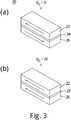
- FIG. 3 is a diagram illustrating an operation concept of a ferromagnetic gate in a reconfigurable logic device using an electrochemical potential according to an embodiment of the present invention.
- the effective magnetic field direction B R of the channel 10a is a positive direction (i.e., the upper direction in FIG. 1 ) and when the current direction is a negative direction -I, the effective magnetic field direction B R of the channel 10a is a negative direction (i.e., the lower part in FIG. 1 ).
- the second semiconductor channel 10b it is configured that when the current direction is a positive direction +1, the effective magnetic field direction B R of the channel 10b is a positive direction (i.e., the upper direction in FIG. 1 ) and when the current direction is a negative direction -I, the effective magnetic field direction B R of the channel 10b is a negative direction (i.e., the lower direction in FIG. 1 ).
- the current direction +I x is defined as 0, and the current direction -I x is defined as 1.
- the direction of the effective magnetic field of the channel is a positive direction +B Ry
- the effective magnetic field direction of the channel is a negative direction -B Ry .
- the semiconductor channel 10 (e.g., 10a or 10b) includes a quantum well layer 11 and cladding layers 12a and 12b and 13a and 13b disposed asymmetrically above and below the quantum well layer 11, and the Rashba effect may convert an electric field into a magnetic field.
- the quantum well layer 11 includes at least one layer of an InAs layer, an InGaAs layer, an InSb layer, and a GaAs layer.
- the cladding layers 12a, 12b, 13a and 13b include at least one or more layers of an InGaAs layer, an InAlAs layer, an InAlSb layer, an AlGaSb layer and an AlGaAs layer.
- the asymmetric structure shown in FIG. 2 is used as a channel in order to generate the Rashba effect inside the semiconductor and increase the electron mobility.
- the relative asymmetry of the layers disclosed in FIG. 2 is shown for convenience.
- the thickness of the layers disclosed in FIG. 2 may be understood in detail by the example numerical values shown in parentheses, not the relative thicknesses shown in the drawings.
- an InAs layer having a small band gap is used as a quantum well layer, and an InGaAs layer and an InAlAs layer are used as a cladding layer to confine charges in a conductive layer.
- the asymmetric structure is formed by placing the doping layer under the quantum well layer and the reason of this is because a strong electric field may be generated according to the slope of the conduction band in the asymmetric channel and the size of the electric field may be adjusted by applying the gate voltage.
- the ferromagnetic gate 20 (e.g., 20a or 20b) includes an upper magnetic layer 22, a lower magnetic layer 26, and an insulating layer 24 interposed between the upper magnetic layer 22 and the lower magnetic layer 26.
- the lower magnetic layer 26 may be arranged to contact the semiconductor channels 10a and 10b.
- the lower magnetic layer 26 may be configured to contact the quantum well layer 11 of the semiconductor channel 20 shown in FIG. 2 .
- the magnetization direction of the upper magnetic layer 22 is fixed and the magnetization direction of the lower magnetic layer 26 is controlled by the gate voltage V G .
- the lower magnetic layer 26 may contact the semiconductor channel 10 and participate in the logic operation.
- Table 1 shows the logic operation of a reconfigurable logic device using an electrochemical potential according to a first embodiment of the present invention.
- a reconfigurable logic device using an electrochemical potential provides an OR logic configuration.
- a reconfigurable logic device using an electrochemical potential which applies the principle of such a logic operation overall, as a logic device that provides an OR logic configuration
- the effective magnetic field direction BR of the channel is a positive direction
- the effective magnetic field direction B R of the channel is configured to have a negative direction
- the gate voltage V G is applied to the first ferromagnetic gate 20a
- the magnetization direction of the first ferromagnetic gate 20a is a negative direction
- the magnetization direction of the second ferromagnetic gate 20b when the gate voltage V G is applied to the second ferromagnetic gate 20b, the magnetization direction of the second ferromagnetic gate 20b is configured to have a positive direction
- the effective magnetic field direction B R of the first semiconductor channel 10a is equal to the magnetization direction of the first ferromagnetic gate 20a
- the first determination value V FM1 is + ⁇ V and if not, the first determination value V FM1 is - ⁇ V
- Table 2 shows the logic operation of a reconfigurable logic device using an electrochemical potential according to a second embodiment of the present invention.
- a reconfigurable logic device using an electrochemical potential provides an AND logic configuration.
- the effective magnetic field direction of the channel is determined as +B Ry and -B Ry since the current directions of X1 and X2 are +I x and -I x , respectively.
- a reconfigurable logic device using an electrochemical potential which applies the principle of such a logic operation overall, as a logic device that provides an AND logic configuration, when the current direction is a positive direction in the semiconductor channels 10a and 10b, the effective magnetic field direction B R of the channel is a positive direction, and when the current direction is a negative direction, the effective magnetic field direction B R of the channel is configured to have a negative direction, and when the gate voltage V G is applied to the first ferromagnetic gate 20a, the magnetization direction of the first ferromagnetic gate 20a is a negative direction, and when the gate voltage V G is applied to the second ferromagnetic gate 20b, the magnetization direction of the second ferromagnetic gate 20b is configured to have a positive direction, and when the effective magnetic field direction B R of the first semiconductor channel 10a is equal to the magnetization direction of the first ferromagnetic gate 20a, the first determination value V FM1 is + ⁇ V and if not, the first determination value V EM1 is - ⁇ V,
- Table 3 shows the logic operation of a reconfigurable logic device using an electrochemical potential according to a third embodiment of the present invention.
- a reconfigurable logic device using an electrochemical potential provides a NAND logic configuration.
- Table 4 shows the logic operation of a reconfigurable logic device using an electrochemical potential according to a fourth embodiment of the present invention.
- a reconfigurable logic device using an electrochemical potential provides a NOR logic configuration.
- a reconfigurable logic device using an electrochemical potential which applies the principle of such a logic operation overall, as a logic device that provides a NOR logic configuration
- the effective magnetic field direction B R of the channel when the current direction is a positive direction in the semiconductor channels 10a and 10b, the effective magnetic field direction B R of the channel is a positive direction, and when the current direction is a negative direction, the effective magnetic field direction B R of the channel is configured to have a negative direction
- the gate voltage V G is applied to the first ferromagnetic gate 20a
- the magnetization direction of the first ferromagnetic gate 20a is a positive direction
- the magnetization direction of the second ferromagnetic gate 20b when the gate voltage V G is applied to the second ferromagnetic gate 20b, the magnetization direction of the second ferromagnetic gate 20b is configured to have a negative direction
- the first determination value V FM1 when the effective magnetic field direction B R of the first semiconductor channel 10a is equal to the magnetization direction of the first ferromagnetic
- Semiconductor-based logic devices are the most important and high value-added field in integrated circuits that perform and process complex functions, and research groups and companies are conducting research thereon.
- the logic devices are a core field for carrying out various operations, and are a key field that leads the semiconductor market together with the memory elements.
- the silicon electronic element technology approaches the physical limit, it is difficult to reduce the size of the element and the nano-sized element process is consuming a lot of cost.
- the emergence of next generation electronic elements has become necessary. For example, research has been conducted on electronic elements using the concept of using spin, which is a quantum mechanical property of electrons, rather than simply improving or miniaturizing existing elements.
- the logic device using existing spintronics mainly generates a large number of spin currents to use the superposition of such currents and uses spin memory as a secondary, and the actual logic function is mostly done by conventional CMOS.
- the above-described invention is a revolutionary invention in which moving away from such an approach, charges are converted directly to spin, and in addition to converting a plurality of input values to a voltage output using a ferromagnetic material, the magnetization direction of the ferromagnetic material is changed to reset a logic function.
- a logic device capable of fundamentally overcoming the physical limitations of silicon electronic element technology, and provided is a reconfigurable logic device using an electrochemical potential.
- a logic device capable of fundamentally overcoming the physical limitations of silicon electronic element technology
- a reconfigurable logic device using an electrochemical potential is provided.
- the scope of the present invention is not limited by such an effect.
Landscapes
- Engineering & Computer Science (AREA)
- Mathematical Physics (AREA)
- Physics & Mathematics (AREA)
- Computer Hardware Design (AREA)
- Computing Systems (AREA)
- General Engineering & Computer Science (AREA)
- Chemical & Material Sciences (AREA)
- Nanotechnology (AREA)
- Power Engineering (AREA)
- Theoretical Computer Science (AREA)
- Crystallography & Structural Chemistry (AREA)
- Manufacturing & Machinery (AREA)
- Hall/Mr Elements (AREA)
- Logic Circuits (AREA)
Abstract
Description
- The present disclosure relates to an electronic element, and more particularly to a reconfigurable logic device.
- Semiconductor-based logic devices are the most important and high value-added field in integrated circuits that perform and process complex functions, and research groups and companies are conducting research thereon. The logic devices are a core field for carrying out various operations, and are a key field that leads the semiconductor market together with the memory elements.
- On the other hand, in the recent logic device, since the silicon electronic element technology approaches the physical limit, it is difficult to reduce the size of the element and the nano-sized element process is consuming a lot of cost. As a result, the emergence of next generation electronic elements becomes necessary. For example, research has been conducted on electronic elements using the concept of using spin, which is a quantum mechanical property of electrons, rather than simply improving or miniaturizing existing elements.
- The present disclosure provides a logic device capable of fundamentally overcoming the physical limitations of silicon electronic element technology, and for example, provides a reconfigurable logic device using an electrochemical potential.
- In accordance with an embodiment, a reconfigurable logic device using an electrochemical potential includes: a first semiconductor channel and a second semiconductor channel, where an effective magnetic field direction of a channel is controlled by a current direction and which are spaced apart from each other; a first ferromagnetic gate contacting the first semiconductor channel and a second ferromagnetic gate contacting the second semiconductor channel, where a magnetization direction is controlled by a gate voltage; and a control unit configured to calculating a difference value corresponding to a difference between a first determination value determined with each different value according to whether the effective magnetic field direction of the first semiconductor channel is equal to the magnetization direction of the first ferromagnetic gate and a second determination value determined with each different value according to whether the effective magnetic field direction of the second semiconductor channel is equal to the magnetization direction of the second ferromagnetic gate, and compare the difference value with a reference value to determine an output value.
- The semiconductor channel may include a quantum well layer and a cladding layer disposed asymmetrically above and below the quantum well layer, or includes a topological insulator or a two-dimensional material layer, wherein the Rashba effect may convert an electric field into a magnetic field.
- The quantum well layer may include at least one layer of an InAs layer, an InGaAs layer, an InSb layer, and a GaAs layer and the cladding layer may include at least one or more layers of an InGaAs layer, an InAlAs layer, an InAlSb layer, an AlGaSb layer and an AlGaAs layer.
- The ferromagnetic gate may include an upper magnetic layer, a lower magnetic layer, and an insulating layer interposed between the upper magnetic layer and the lower magnetic layer, wherein the magnetization direction of the upper magnetic layer may be fixed but the magnetization direction of the lower magnetic layer may be controlled by the applied gate voltage such that the magnetization direction of the lower magnetic layer determines a logic function, wherein the lower magnetic layer may be disposed to contact the semiconductor channel.
- The reconfigurable logic device may provide an OR logic configuration, wherein when the current direction is a first direction in the semiconductor channel, the effective magnetic field direction of the channel is a second direction, and when the current direction is a third direction opposite the first direction, the effective magnetic field direction of the channel is configured to have a fourth direction opposite the second direction, wherein a first gate voltage is applied to the first ferromagnetic gate such that the magnetization direction of the lower magnetic layer of the first ferromagnetic gate is parallel to the fourth direction, and a second gate voltage is applied to the second ferromagnetic gate such that the magnetization direction of the lower magnetic layer of the second ferromagnetic gate is parallel to the second direction, wherein when the effective magnetic field direction of the first semiconductor channel is equal to the magnetization direction of the lower magnetic layer of the first ferromagnetic gate, the first determination value is +ΔV and if not, the first determination value is -ΔV, wherein when the effective magnetic field direction of the second semiconductor channel is equal to the magnetization direction of the lower magnetic layer of the second ferromagnetic gate, the second determination value is +ΔV and, if not, the second determination value is -ΔV, wherein it is determined that the difference value corresponding to the difference between the first determination value and the second determination value has a value of 1, if it is compared with -ΔV, that is, the reference value, and relatively large, and has a value of 0, if it is relatively small, so that when the current direction in the first semiconductor channel has the first direction and the current direction in the second semiconductor channel has the first direction, the output value has a value of 0, and when the current direction in the first semiconductor channel has the first direction and the current direction in the second semiconductor channel has the third direction, the output value has a value of 1, and when the current direction in the first semiconductor channel has the third direction and the current direction in the second semiconductor channel has the first direction, the output value has a value of 1, and when the current direction in the first semiconductor channel has the third direction and the current direction in the second semiconductor channel has the third direction, the output value has a value of 1.
- The reconfigurable logic device may provide an AND logic configuration, wherein when the current direction is a first direction in the semiconductor channel, the effective magnetic field direction of the channel is a second direction, and when the current direction is a third direction opposite the first direction, the effective magnetic field direction of the channel is configured to have a fourth direction opposite the second direction, wherein a first gate voltage is applied to the first ferromagnetic gate such that the magnetization direction of the lower magnetic layer of the first ferromagnetic gate is parallel to the fourth direction, and a second gate voltage is applied to the second ferromagnetic gate such that the magnetization direction of the lower magnetic layer of the second ferromagnetic gate is parallel to the second direction, wherein when the effective magnetic field direction of the first semiconductor channel is equal to the magnetization direction of the lower magnetic layer of the first ferromagnetic gate, the first determination value is +ΔV and if not, the first determination value is -ΔV, wherein when the effective magnetic field direction of the second semiconductor channel is equal to the magnetization direction of the lower magnetic layer of the second ferromagnetic gate, the second determination value is +ΔV and, if not, the second determination value is -ΔV, wherein it is determined that the difference value corresponding to the difference between the first determination value and the second determination value has a value of 1, if it is compared with +ΔV, that is, the reference value, and relatively large, and has a value of 0, if it is relatively small, so that when the current direction in the first semiconductor channel has the first direction and the current direction in the second semiconductor channel has the first direction, the output value has a value of 0, and when the current direction in the first semiconductor channel has the first direction and the current direction in the second semiconductor channel has the third direction, the output value has a value of 0, and when the current direction in the first semiconductor channel has the third direction and the current direction in the second semiconductor channel has the first direction, the output value has a value of 0, and when the current direction in the first semiconductor channel has the third direction and the current direction in the second semiconductor channel has the third direction, the output value has a value of 1.
- The reconfigurable logic device may provide a NAND logic configuration, wherein when the current direction is a first direction in the semiconductor channel, the effective magnetic field direction of the channel is a second direction, and when the current direction is a third direction opposite the first direction, the effective magnetic field direction of the channel is configured to have a fourth direction opposite the second direction, wherein a second gate voltage is applied to the first ferromagnetic gate such that the magnetization direction of the lower magnetic layer of the first ferromagnetic gate is parallel to the second direction, and a first gate voltage is applied to the second ferromagnetic gate such that the magnetization direction of the lower magnetic layer of the second ferromagnetic gate is parallel to the fourth direction, wherein when the effective magnetic field direction of the first semiconductor channel is equal to the magnetization direction of the lower magnetic layer of the first ferromagnetic gate, the first determination value is +ΔV and if not, the first determination value is -ΔV, wherein when the effective magnetic field direction of the second semiconductor channel is equal to the magnetization direction of the lower magnetic layer of the second ferromagnetic gate, the second determination value is +ΔV and, if not, the second determination value is -ΔV, wherein it is determined that the difference value corresponding to the difference between the first determination value and the second determination value has a value of 1, if it is compared with -ΔV, that is, the reference value, and relatively large, and has a value of 0, if it is relatively small, so that when the current direction in the first semiconductor channel has the first direction and the current direction in the second semiconductor channel has the first direction, the output value has a value of 1, and when the current direction in the first semiconductor channel has the first direction and the current direction in the second semiconductor channel has the third direction, the output value has a value of 1, and when the current direction in the first semiconductor channel has the third direction and the current direction in the second semiconductor channel has the first direction, the output value has a value of 1, and when the current direction in the first semiconductor channel has the third direction and the current direction in the second semiconductor channel has the third direction, the output value has a value of 0.
- The reconfigurable logic device may provide a NOR logic configuration, wherein when the current direction is a first direction in the semiconductor channel, the effective magnetic field direction of the channel is a second direction, and when the current direction is a third direction opposite the first direction, the effective magnetic field direction of the channel is configured to have a fourth direction opposite the second direction, wherein a second gate voltage is applied to the first ferromagnetic gate such that the magnetization direction of the lower magnetic layer of the first ferromagnetic gate is parallel to the second direction, and a first gate voltage is applied to the second ferromagnetic gate such that the magnetization direction of the lower magnetic layer of the second ferromagnetic gate is parallel to the fourth direction, wherein when the effective magnetic field direction of the first semiconductor channel is equal to the magnetization direction of the lower magnetic layer of the first ferromagnetic gate, the first determination value is +ΔV and if not, the first determination value is -ΔV, wherein when the effective magnetic field direction of the second semiconductor channel is equal to the magnetization direction of the lower magnetic layer of the second ferromagnetic gate, the second determination value is +ΔV and, if not, the second determination value is -ΔV, wherein it is determined that the difference value corresponding to the difference between the first determination value and the second determination value has a value of 1, if it is compared with +ΔV, that is, the reference value, and relatively large, and has a value of 0, if it is relatively small, so that when the current direction in the first semiconductor channel has the first direction and the current direction in the second semiconductor channel has the first direction, the output value has a value of 1, and when the current direction in the first semiconductor channel has the first direction and the current direction in the second semiconductor channel has the third direction, the output value has a value of 0, and when the current direction in the first semiconductor channel has the third direction and the current direction in the second semiconductor channel has the first direction, the output value has a value of 0, and when the current direction in the first semiconductor channel has the third direction and the current direction in the second semiconductor channel has the third direction, the output value has a value of 0.
- Exemplary embodiments can be understood in more detail from the following description taken in conjunction with the accompanying drawings, in which:
-
FIG. 1 is a conceptual diagram illustrating the configuration of a reconfigurable logic device using an electrochemical potential according to an embodiment of the present invention; -
FIG. 2 is a cross-sectional view illustrating the configuration of a semiconductor channel in a reconfigurable logic device using an electrochemical potential according to an embodiment of the present invention; and -
FIG. 3 is a diagram illustrating an operation concept of a ferromagnetic gate in a reconfigurable logic device using an electrochemical potential according to an embodiment of the present invention. - Hereinafter, embodiments of the present invention are described in more detail with reference to the accompanying drawings. However, the present invention may be embodied in different forms and should not be construed as limited to the embodiments set forth herein, and rather, these embodiments are provided so that this disclosure will be thorough and complete, and will fully convey the scope of the present invention to those skilled in the art. Also, at least some of the components may be exaggerated or reduced in size for convenience of explanation. Like numbers refer to like elements throughout the drawings.
- It may be interpreted that throughout the specification, when an element such as a layer or a region is referred to as being "on" another element, it may be directly "on" the other element or there may be other elements therebetween. On the other hand, when an element is referred to as being "directly on" another element, it is interpreted that there are no other elements therebetween.
-
FIG. 1 is a conceptual diagram illustrating the configuration of a reconfigurable logic device using an electrochemical potential according to an embodiment of the present invention,FIG. 2 is a cross-sectional view illustrating the configuration of a semiconductor channel in a reconfigurable logic device using an electrochemical potential according to an embodiment of the present invention, andFIG. 3 is a diagram illustrating an operation concept of a ferromagnetic gate in a reconfigurable logic device using an electrochemical potential according to an embodiment of the present invention. - Referring to
FIGS. 1 to 3 , a reconfigurable logic device using an electrochemical potential according to an embodiment of the present invention includes afirst semiconductor channel 10a and asecond semiconductor channel 10b, where an effective magnetic field direction BR of a channel is controlled by a current direction and which are spaced apart from each other; and a firstferromagnetic gate 20a contacting thefirst semiconductor channel 10a and a secondferromagnetic gate 20b contacting thesecond semiconductor channel 10b, where a magnetization direction is controlled by a gate voltage VG. - Further, a reconfigurable logic device using an electrochemical potential according to an embodiment of the present invention includes a
control unit 30 for calculating a difference value VOUT corresponding to a difference between a first determination value VFM1 determined with each different value according to whether the effective magnetic field direction BR of thefirst semiconductor channel 10a is equal to the magnetization direction of the firstferromagnetic gate 20a and a second determination value VFM2 determined with each different value according to whether the effective magnetic field direction BR of thesecond semiconductor channel 10b is equal to the magnetization direction of the secondferromagnetic gate 20b, and comparing the difference value VOUT with a reference value Vref to determine an output value Y. - Referring to
FIG. 1 , in thefirst semiconductor channel 10a of the reconfigurable logic device using an electrochemical potential according to an embodiment of the present invention, it is configured that when the current direction is a positive direction +1, the effective magnetic field direction BR of thechannel 10a is a positive direction (i.e., the upper direction inFIG. 1 ) and when the current direction is a negative direction -I, the effective magnetic field direction BR of thechannel 10a is a negative direction (i.e., the lower part inFIG. 1 ). In addition, in thesecond semiconductor channel 10b, it is configured that when the current direction is a positive direction +1, the effective magnetic field direction BR of thechannel 10b is a positive direction (i.e., the upper direction inFIG. 1 ) and when the current direction is a negative direction -I, the effective magnetic field direction BR of thechannel 10b is a negative direction (i.e., the lower direction inFIG. 1 ). - Referring to
FIG. 1 , when the horizontal direction is assumed to extend in the x axis and the vertical direction is assumed to extend in the y axis, the current direction +Ix is defined as 0, and the current direction -Ix is defined as 1. In a semiconductor channel, when the current direction is the positive direction +Ix, the direction of the effective magnetic field of the channel is a positive direction +BRy, and in a semiconductor channel, when the current direction is the negative direction - Ix, the effective magnetic field direction of the channel is a negative direction -BRy. - Referring to
FIG. 2 , in a reconfigurable logic device using an electrochemical potential according to an embodiment of the present invention, the semiconductor channel 10 (e.g., 10a or 10b) includes aquantum well layer 11 and claddinglayers quantum well layer 11, and the Rashba effect may convert an electric field into a magnetic field. Thequantum well layer 11 includes at least one layer of an InAs layer, an InGaAs layer, an InSb layer, and a GaAs layer. Thecladding layers - In addition, the semiconductor channel 10 (e.g., 10a or 10b) includes a topological insulator or a two-dimensional material layer in addition to a quantum well layer, and the Rashba effect may convert an electric field into a magnetic field. In a reconfigurable logic device using an electrochemical potential according to an embodiment of the present invention, a spin precession is required for a transistor operation. The basic principle for generating such a phenomenon is called a Rashba effect. The Rashba effect is a phenomenon that is central to the implementation of spin transistors in a principle of converting an electric field to a magnetic field. Assuming an arbitrary three-axis space, the basic principle is that a y-direction magnetic field is induced when electrons traveling in the x-direction receive an electric field in the z-direction. Here, the electric field may occur inside the semiconductor's heterogeneous structure and the size of the electric field may be adjusted by applying an external electric field.
- The asymmetric structure shown in
FIG. 2 is used as a channel in order to generate the Rashba effect inside the semiconductor and increase the electron mobility. The relative asymmetry of the layers disclosed inFIG. 2 is shown for convenience. For example, the thickness of the layers disclosed inFIG. 2 may be understood in detail by the example numerical values shown in parentheses, not the relative thicknesses shown in the drawings. - In the Rashba effect, since the asymmetry of the bonding surface plays an important role rather than the material itself, it is important to implement a sophisticated heterogeneous bonding structure. In an embodiment of the present invention, an InAs layer having a small band gap is used as a quantum well layer, and an InGaAs layer and an InAlAs layer are used as a cladding layer to confine charges in a conductive layer. Here, the asymmetric structure is formed by placing the doping layer under the quantum well layer and the reason of this is because a strong electric field may be generated according to the slope of the conduction band in the asymmetric channel and the size of the electric field may be adjusted by applying the gate voltage.
- Referring to
FIG. 3 , in the reconfigurable logic device using an electrochemical potential according to an embodiment of the present invention, the ferromagnetic gate 20 (e.g., 20a or 20b) includes an uppermagnetic layer 22, a lowermagnetic layer 26, and aninsulating layer 24 interposed between the uppermagnetic layer 22 and the lowermagnetic layer 26. The lowermagnetic layer 26 may be arranged to contact thesemiconductor channels magnetic layer 26 may be configured to contact thequantum well layer 11 of thesemiconductor channel 20 shown inFIG. 2 . - The magnetization direction of the upper
magnetic layer 22 may be fixed but the magnetization direction of the lowermagnetic layer 26 may be controlled by the applied gate voltage VG. When the gate voltage VG is 0 V (seeFIG. 3A ), the magnetization direction of the uppermagnetic layer 22 and the magnetization direction of the lowermagnetic layer 26 may be opposite to each other. When the gate voltage VG is 1 V (seeFIG. 3B ), the magnetization direction of the uppermagnetic layer 22 may be fixed but the magnetization direction of the lowermagnetic layer 26 may be changed to be identical to the magnetization direction of the uppermagnetic layer 22. - That is, in a reconfigurable logic device using an electrochemical potential according to an embodiment of the present invention, the magnetization direction of the upper
magnetic layer 22 is fixed and the magnetization direction of the lowermagnetic layer 26 is controlled by the gate voltage VG. The lowermagnetic layer 26 may contact thesemiconductor channel 10 and participate in the logic operation. - In a reconfigurable logic device using an electrochemical potential according to the technical idea of the present invention described above, it is possible to perform function switching and logic functions without changing the magnetic field. Hereinafter, the principle of logic operation will be described with specific examples.
- Table 1 shows the logic operation of a reconfigurable logic device using an electrochemical potential according to a first embodiment of the present invention. A reconfigurable logic device using an electrochemical potential provides an OR logic configuration.
[Table 1] (X1,X2) VFM1,VFM2 VOUT Y (0,0) -ΔV,+ΔV -2ΔV 0 (0,1) -ΔV,- ΔV 0 1 (1,0) +ΔV,+ ΔV 0 1 (1,1) +ΔV,-ΔV +2ΔV 1 - Referring to Table 1, in a reconfigurable logic device using an electrochemical potential to provide an OR logic configuration, when the input value is (0,0), the effective magnetic field direction of the channel is determined as +BRy since the current directions of X1 and X2 are all +Ix. In the case of an OR gate, since the magnetization directions of the first ferromagnetic gate FM1 and the second ferromagnetic gate FM2 that are already set are -My and +My, the magnetization direction of the lower magnetic layer of the first ferromagnetic gate and the effective magnetic field direction of the first semiconductor channel are anti-parallel and have a -ΔV value, and the magnetization direction of the lower magnetic layer of the second ferromagnetic gate and the effective magnetic field direction of the second semiconductor channel are parallel and have a +ΔV value, and since it is determined that VOUT = VFM1 - VFM2 = (-ΔV) - (+ΔV) = -2ΔV and it is less than Vref = -ΔV, the output value is determined as 0.
- In a reconfigurable logic device using an electrochemical potential, which applies the principle of such a logic operation overall, as a logic device that provides an OR logic configuration, when the current direction is a positive direction in the semiconductor channels 10a and 10b, the effective magnetic field direction BR of the channel is a positive direction, and when the current direction is a negative direction, the effective magnetic field direction BR of the channel is configured to have a negative direction, and when the gate voltage VG is applied to the first ferromagnetic gate 20a, the magnetization direction of the first ferromagnetic gate 20a is a negative direction, and when the gate voltage VG is applied to the second ferromagnetic gate 20b, the magnetization direction of the second ferromagnetic gate 20b is configured to have a positive direction, and when the effective magnetic field direction BR of the first semiconductor channel 10a is equal to the magnetization direction of the first ferromagnetic gate 20a, the first determination value VFM1 is +ΔV and if not, the first determination value VFM1 is -ΔV, and when the effective magnetic field direction BR of the second semiconductor channel 10b is equal to the magnetization direction of the second ferromagnetic gate 20b, the second determination value VFM2 is +ΔV and, if not, the second determination value VFM2 is -ΔV, and it is determined that the difference value VOUT corresponding to the difference between the first determination value VFM1 and the second determination value VFM2 has a value of 1, if it is compared with -ΔV, that is, the reference value Vref, and relatively large, and has a value of 0, if it is relatively small, so that when the current direction in the first semiconductor channel 10a has a positive direction and the current direction in the second semiconductor channel 10b has a positive direction, the output value has a value of 0, and when the current direction in the first semiconductor channel 10a has a positive direction and the current direction in the second semiconductor channel 10b has a negative direction, the output value has a value of 1, and when the current direction in the first semiconductor channel 10a has a negative direction and the current direction in the second semiconductor channel 10b has a positive direction, the output value has a value of 1, and when the current direction in the first semiconductor channel 10a has a negative direction and the current direction in the second semiconductor channel 10b has a negative direction, the output value has a value of 1.
- Table 2 shows the logic operation of a reconfigurable logic device using an electrochemical potential according to a second embodiment of the present invention. A reconfigurable logic device using an electrochemical potential provides an AND logic configuration.
[Table 2] (X1,X2) VFM1,VFM2 VOUT Y (0,0) -ΔV,+ΔV -2ΔV 0 (0,1) -ΔV,- ΔV 0 0 (1,0) +ΔV,+ ΔV 0 0 (1,1) +ΔV,-ΔV +2ΔV 1 - Referring to Table 2, in a reconfigurable logic device using an electrochemical potential to provide an AND logic configuration, when the input value is (0.1), the effective magnetic field direction of the channel is determined as +BRy and -BRy since the current directions of X1 and X2 are +Ix and -Ix, respectively. In the case of an AND gate, since the magnetization directions of the first ferromagnetic gate FM1 and the second ferromagnetic gate FM2 that are already set are -My and +My, the magnetization direction of the lower magnetic layer of the first ferromagnetic gate and the effective magnetic field direction of the first semiconductor channel are parallel and have a +ΔV value, and the magnetization direction of the lower magnetic layer of the second ferromagnetic gate and the effective magnetic field direction of the second semiconductor channel are parallel and have a +ΔV value, and since it is determined that VOUT = VFM1 - VFM2 = (+ΔV) - (+ΔV) = 0 and it is less than Vref = +ΔV, the output value is determined as 0.
- In a reconfigurable logic device using an electrochemical potential, which applies the principle of such a logic operation overall, as a logic device that provides an AND logic configuration, when the current direction is a positive direction in the semiconductor channels 10a and 10b, the effective magnetic field direction BR of the channel is a positive direction, and when the current direction is a negative direction, the effective magnetic field direction BR of the channel is configured to have a negative direction, and when the gate voltage VG is applied to the first ferromagnetic gate 20a, the magnetization direction of the first ferromagnetic gate 20a is a negative direction, and when the gate voltage VG is applied to the second ferromagnetic gate 20b, the magnetization direction of the second ferromagnetic gate 20b is configured to have a positive direction, and when the effective magnetic field direction BR of the first semiconductor channel 10a is equal to the magnetization direction of the first ferromagnetic gate 20a, the first determination value VFM1 is +ΔV and if not, the first determination value VEM1 is -ΔV, and when the effective magnetic field direction BR of the second semiconductor channel 10b is equal to the magnetization direction of the second ferromagnetic gate 20b, the second determination value VFM2 is +ΔV and, if not, the second determination value VFM2 is -ΔV, and it is determined that the difference value VOUT corresponding to the difference between the first determination value VFM1 and the second determination value VFM2 has a value of 1, if it is compared with +ΔV, that is, the reference value Vref, and relatively large, and has a value of 0, if it is relatively small, so that when the current direction in the first semiconductor channel 10a has a positive direction and the current direction in the second semiconductor channel 10b has a positive direction, the output value has a value of 0, and when the current direction in the first semiconductor channel 10a has a positive direction and the current direction in the second semiconductor channel 10b has a negative direction, the output value has a value of 0, and when the current direction in the first semiconductor channel 10a has a negative direction and the current direction in the second semiconductor channel 10b has a positive direction, the output value has a value of 0, and when the current direction in the first semiconductor channel 10a has a negative direction and the current direction in the second semiconductor channel 10b has a negative direction, the output value has a value of 1.
- Table 3 shows the logic operation of a reconfigurable logic device using an electrochemical potential according to a third embodiment of the present invention. A reconfigurable logic device using an electrochemical potential provides a NAND logic configuration.
[Table 3] (X1,X2) VFM1,VFM2 VOUT Y (0,0) +ΔV,-ΔV +2ΔV 1 (0,1) +ΔV,+ ΔV 0 1 (1,0) -ΔV,- ΔV 0 1 (1,1) -ΔV,+ΔV - 2ΔV 0 - Referring to Table 3, in a reconfigurable logic device using an electrochemical potential to provide a NAND logic configuration, when the input value is (0,0), the effective magnetic field direction of the channel is determined as +BRy since the current directions of X1 and X2 are all +Ix. In the case of a NAND gate, since the magnetization directions of the first ferromagnetic gate FM1 and the second ferromagnetic gate FM2 that are already set are +My and -My, the magnetization direction of the lower magnetic layer of the first ferromagnetic gate and the effective magnetic field direction of the first semiconductor channel are parallel and have a +ΔV value, and the magnetization direction of the lower magnetic layer of the second ferromagnetic gate and the effective magnetic field direction of the second semiconductor channel are anti-parallel and have a -ΔV value, and since it is determined that VOUT = VFM1 - VFM2 = (+ΔV) - (-ΔV) = +2ΔV and it is greater than Vref = -ΔV, the output value is determined as 1.
- In a reconfigurable logic device using an electrochemical potential, which applies the principle of such a logic operation overall, as a logic device that provides a NAND logic configuration, when the current direction is a positive direction in the semiconductor channels 10a and 10b, the effective magnetic field direction BR of the channel is a positive direction, and when the current direction is a negative direction, the effective magnetic field direction BR of the channel is configured to have a negative direction, and when the gate voltage VG is applied to the first ferromagnetic gate 20a, the magnetization direction of the first ferromagnetic gate 20a is a positive direction, and when the gate voltage VG is applied to the second ferromagnetic gate 20b, the magnetization direction of the second ferromagnetic gate 20b is configured to have a negative direction, and when the effective magnetic field direction BR of the first semiconductor channel 10a is equal to the magnetization direction of the first ferromagnetic gate 20a, the first determination value VFM1 is +ΔV and if not, the first determination value VFM1 is -ΔV, and when the effective magnetic field direction BR of the second semiconductor channel 10b is equal to the magnetization direction of the second ferromagnetic gate 20b, the second determination value VFM2 is +ΔV and, if not, the second determination value VFM2 is -ΔV, and it is determined that the difference value VOUT corresponding to the difference between the first determination value VFM1 and the second determination value VFM2 has a value of 1, if it is compared with -ΔV, that is, the reference value Vref, and relatively large, and has a value of 0, if it is relatively small, so that when the current direction in the first semiconductor channel 10a has a positive direction and the current direction in the second semiconductor channel 10b has a positive direction, the output value has a value of 1, and when the current direction in the first semiconductor channel 10a has a positive direction and the current direction in the second semiconductor channel 10b has a negative direction, the output value has a value of 1, and when the current direction in the first semiconductor channel 10a has a negative direction and the current direction in the second semiconductor channel 10b has a positive direction, the output value has a value of 1, and when the current direction in the first semiconductor channel 10a has a negative direction and the current direction in the second semiconductor channel 10b has a negative direction, the output value has a value of 0.
- Table 4 shows the logic operation of a reconfigurable logic device using an electrochemical potential according to a fourth embodiment of the present invention. A reconfigurable logic device using an electrochemical potential provides a NOR logic configuration.
[Table 4] (X1,X2) VFM1,VFM2 VOUT Y (0,0) +ΔV,-ΔV +2ΔV 1 (0,1) +ΔV,+ ΔV 0 0 (1,0) -ΔV,- ΔV 0 0 (1,1) -ΔV,+ΔV - 2ΔV 0 - Referring to Table 4, in a reconfigurable logic device using an electrochemical potential to provide a NOR logic configuration, when the input value is (1.1), the effective magnetic field direction of the channel is determined as -BRy since the current directions of X1 and X2 are all -Ix. In the case of a NOR gate, since the magnetization directions of the first ferromagnetic gate FM1 and the second ferromagnetic gate FM2 that are already set are +My and -My, the magnetization direction of the lower magnetic layer of the first ferromagnetic gate and the effective magnetic field direction of the first semiconductor channel are anti-parallel and have a -ΔV value, and the magnetization direction of the lower magnetic layer of the second ferromagnetic gate and the effective magnetic field direction of the second semiconductor channel are parallel and have a +ΔV value, and since it is determined that VOUT = VFM1 - VFM2 = (-ΔV) - (+ΔV) = -2ΔV and it is less than Vref = -ΔV, the output value is determined as 0.
- In a reconfigurable logic device using an electrochemical potential, which applies the principle of such a logic operation overall, as a logic device that provides a NOR logic configuration, when the current direction is a positive direction in the semiconductor channels 10a and 10b, the effective magnetic field direction BR of the channel is a positive direction, and when the current direction is a negative direction, the effective magnetic field direction BR of the channel is configured to have a negative direction, and when the gate voltage VG is applied to the first ferromagnetic gate 20a, the magnetization direction of the first ferromagnetic gate 20a is a positive direction, and when the gate voltage VG is applied to the second ferromagnetic gate 20b, the magnetization direction of the second ferromagnetic gate 20b is configured to have a negative direction, and when the effective magnetic field direction BR of the first semiconductor channel 10a is equal to the magnetization direction of the first ferromagnetic gate 20a, the first determination value VFM1 is +ΔV and if not, the first determination value VFM1 is -ΔV, and when the effective magnetic field direction BR of the second semiconductor channel 10b is equal to the magnetization direction of the second ferromagnetic gate 20b, the second determination value VFM2 is +ΔV and, if not, the second determination value VFM2 is -ΔV, and it is determined that the difference value VOUT corresponding to the difference between the first determination value VFM1 and the second determination value VFM2 has a value of 1, if it is compared with +ΔV, that is, the reference value Vref, and relatively large, and has a value of 0, if it is relatively small, so that when the current direction in the first semiconductor channel 10a has a positive direction and the current direction in the second semiconductor channel 10b has a positive direction, the output value has a value of 1, and when the current direction in the first semiconductor channel 10a has a positive direction and the current direction in the second semiconductor channel 10b has a negative direction, the output value has a value of 0, and when the current direction in the first semiconductor channel 10a has a negative direction and the current direction in the second semiconductor channel 10b has a positive direction, the output value has a value of 0, and when the current direction in the first semiconductor channel 10a has a negative direction and the current direction in the second semiconductor channel 10b has a negative direction, the output value has a value of 0.
- Semiconductor-based logic devices are the most important and high value-added field in integrated circuits that perform and process complex functions, and research groups and companies are conducting research thereon. The logic devices are a core field for carrying out various operations, and are a key field that leads the semiconductor market together with the memory elements. In the recent logic device, since the silicon electronic element technology approaches the physical limit, it is difficult to reduce the size of the element and the nano-sized element process is consuming a lot of cost. As a result, the emergence of next generation electronic elements has become necessary. For example, research has been conducted on electronic elements using the concept of using spin, which is a quantum mechanical property of electrons, rather than simply improving or miniaturizing existing elements. The logic device using existing spintronics mainly generates a large number of spin currents to use the superposition of such currents and uses spin memory as a secondary, and the actual logic function is mostly done by conventional CMOS. The above-described invention is a revolutionary invention in which moving away from such an approach, charges are converted directly to spin, and in addition to converting a plurality of input values to a voltage output using a ferromagnetic material, the magnetization direction of the ferromagnetic material is changed to reset a logic function.
- According to embodiments of the present invention, provided is a logic device capable of fundamentally overcoming the physical limitations of silicon electronic element technology, and provided is a reconfigurable logic device using an electrochemical potential. Of course, the scope of the present invention is not limited by such an effect.
- Although the reconfigurable logic device using an electrochemical potential has been described with reference to the specific embodiments, it is not limited thereto. Therefore, it will be readily understood by those skilled in the art that various modifications and changes can be made thereto without departing from the scope of the present invention defined by the appended claims.
Claims (8)
- A reconfigurable logic device using an electrochemical potential, the reconfigurable logic device comprising:a first semiconductor channel and a second semiconductor channel, where an effective magnetic field direction of a channel is controlled by a current direction and which are spaced apart from each other;a first ferromagnetic gate contacting the first semiconductor channel and a second ferromagnetic gate contacting the second semiconductor channel, where a magnetization direction is controlled by a gate voltage; anda control unit configured to calculating a difference value corresponding to a difference between a first determination value determined with each different value according to whether the effective magnetic field direction of the first semiconductor channel is equal to the magnetization direction of the first ferromagnetic gate and a second determination value determined with each different value according to whether the effective magnetic field direction of the second semiconductor channel is equal to the magnetization direction of the second ferromagnetic gate, and compare the difference value with a reference value to determine an output value.
- The reconfigurable logic device of claim 1, wherein the semiconductor channel comprises a quantum well layer and a cladding layer disposed asymmetrically above and below the quantum well layer, or comprises a topological insulator or a two-dimensional material layer,
wherein the Rashba effect converts an electric field into a magnetic field. - The reconfigurable logic device of claim 2, wherein the quantum well layer comprises at least one layer of an InAs layer, an InGaAs layer, an InSb layer, and a GaAs layer and the cladding layer comprises at least one or more layers of an InGaAs layer, an InAlAs layer, an InAlSb layer, an AlGaSb layer and an AlGaAs layer.
- The reconfigurable logic device of any one of the preceding claims, wherein the ferromagnetic gate comprises an upper magnetic layer, a lower magnetic layer, and an insulating layer interposed between the upper magnetic layer and the lower magnetic layer,
wherein the magnetization direction of the upper magnetic layer is fixed but the magnetization direction of the lower magnetic layer is controlled by the applied gate voltage such that the magnetization direction of the lower magnetic layer determines a logic function,
wherein the lower magnetic layer is disposed to contact the semiconductor channel. - The reconfigurable logic device of claim 4, which provides an OR logic configuration,
wherein when the current direction is a first direction in the semiconductor channel, the effective magnetic field direction of the channel is a second direction, and when the current direction is a third direction opposite the first direction, the effective magnetic field direction of the channel is configured to have a fourth direction opposite the second direction,
wherein a first gate voltage is applied to the first ferromagnetic gate such that the magnetization direction of the lower magnetic layer of the first ferromagnetic gate is parallel to the fourth direction, and a second gate voltage is applied to the second ferromagnetic gate such that the magnetization direction of the lower magnetic layer of the second ferromagnetic gate is parallel to the second direction,
wherein when the effective magnetic field direction of the first semiconductor channel is equal to the magnetization direction of the lower magnetic layer of the first ferromagnetic gate, the first determination value is +ΔV and if not, the first determination value is -ΔV,
wherein when the effective magnetic field direction of the second semiconductor channel is equal to the magnetization direction of the lower magnetic layer of the second ferromagnetic gate, the second determination value is +ΔV and if not, the second determination value is -ΔV,
wherein it is determined that the difference value corresponding to the difference between the first determination value and the second determination value has a value of 1, if it is compared with -ΔV, that is, the reference value, and relatively large, and has a value of 0, if it is relatively small, so that when the current direction in the first semiconductor channel has the first direction and the current direction in the second semiconductor channel has the first direction, the output value has a value of 0, and when the current direction in the first semiconductor channel has the first direction and the current direction in the second semiconductor channel has the third direction, the output value has a value of 1, and when the current direction in the first semiconductor channel has the third direction and the current direction in the second semiconductor channel has the first direction, the output value has a value of 1, and when the current direction in the first semiconductor channel has the third direction and the current direction in the second semiconductor channel has the third direction, the output value has a value of 1. - The reconfigurable logic device of claim 4, which provides an AND logic configuration,
wherein when the current direction is a first direction in the semiconductor channel, the effective magnetic field direction of the channel is a second direction, and when the current direction is a third direction opposite the first direction, the effective magnetic field direction of the channel is configured to have a fourth direction opposite the second direction,
wherein a first gate voltage is applied to the first ferromagnetic gate such that the magnetization direction of the lower magnetic layer of the first ferromagnetic gate is parallel to the fourth direction, and a second gate voltage is applied to the second ferromagnetic gate such that the magnetization direction of the lower magnetic layer of the second ferromagnetic gate is parallel to the second direction,
wherein when the effective magnetic field direction of the first semiconductor channel is equal to the magnetization direction of the lower magnetic layer of the first ferromagnetic gate, the first determination value is +ΔV and if not, the first determination value is -ΔV,
wherein when the effective magnetic field direction of the second semiconductor channel is equal to the magnetization direction of the lower magnetic layer of the second ferromagnetic gate, the second determination value is +ΔV and if not, the second determination value is -ΔV,
wherein it is determined that the difference value corresponding to the difference between the first determination value and the second determination value has a value of 1, if it is compared with +ΔV, that is, the reference value, and relatively large, and has a value of 0, if it is relatively small, so that when the current direction in the first semiconductor channel has the first direction and the current direction in the second semiconductor channel has the first direction, the output value has a value of 0, and when the current direction in the first semiconductor channel has the first direction and the current direction in the second semiconductor channel has the third direction, the output value has a value of 0, and when the current direction in the first semiconductor channel has the third direction and the current direction in the second semiconductor channel has the first direction, the output value has a value of 0, and when the current direction in the first semiconductor channel has the third direction and the current direction in the second semiconductor channel has the third direction, the output value has a value of 1. - The reconfigurable logic device of claim 4, which provides a NAND logic configuration,
wherein when the current direction is a first direction in the semiconductor channel, the effective magnetic field direction of the channel is a second direction, and when the current direction is a third direction opposite the first direction, the effective magnetic field direction of the channel is configured to have a fourth direction opposite the second direction,
wherein a second gate voltage is applied to the first ferromagnetic gate such that the magnetization direction of the lower magnetic layer of the first ferromagnetic gate is parallel to the second direction, and a first gate voltage is applied to the second ferromagnetic gate such that the magnetization direction of the lower magnetic layer of the second ferromagnetic gate is parallel to the fourth direction,
wherein when the effective magnetic field direction of the first semiconductor channel is equal to the magnetization direction of the lower magnetic layer of the first ferromagnetic gate, the first determination value is +ΔV and if not, the first determination value is -ΔV,
wherein when the effective magnetic field direction of the second semiconductor channel is equal to the magnetization direction of the lower magnetic layer of the second ferromagnetic gate, the second determination value is +ΔV and if not, the second determination value is -ΔV,
wherein it is determined that the difference value corresponding to the difference between the first determination value and the second determination value has a value of 1, if it is compared with -ΔV, that is, the reference value, and relatively large, and has a value of 0, if it is relatively small, so that when the current direction in the first semiconductor channel has the first direction and the current direction in the second semiconductor channel has the first direction, the output value has a value of 1, and when the current direction in the first semiconductor channel has the first direction and the current direction in the second semiconductor channel has the third direction, the output value has a value of 1, and when the current direction in the first semiconductor channel has the third direction and the current direction in the second semiconductor channel has the first direction, the output value has a value of 1, and when the current direction in the first semiconductor channel has the third direction and the current direction in the second semiconductor channel has the third direction, the output value has a value of 0. - The reconfigurable logic device of claim 4, which provides a NOR logic configuration,
wherein when the current direction is a first direction in the semiconductor channel, the effective magnetic field direction of the channel is a second direction, and when the current direction is a third direction opposite the first direction, the effective magnetic field direction of the channel is configured to have a fourth direction opposite the second direction,
wherein a second gate voltage is applied to the first ferromagnetic gate such that the magnetization direction of the lower magnetic layer of the first ferromagnetic gate is parallel to the second direction, and a first gate voltage is applied to the second ferromagnetic gate such that the magnetization direction of the lower magnetic layer of the second ferromagnetic gate is parallel to the fourth direction,
wherein when the effective magnetic field direction of the first semiconductor channel is equal to the magnetization direction of the lower magnetic layer of the first ferromagnetic gate, the first determination value is +ΔV and if not, the first determination value is -ΔV,
wherein when the effective magnetic field direction of the second semiconductor channel is equal to the magnetization direction of the lower magnetic layer of the second ferromagnetic gate, the second determination value is +ΔV and if not, the second determination value is -ΔV,
wherein it is determined that the difference value corresponding to the difference between the first determination value and the second determination value has a value of 1, if it is compared with +ΔV, that is, the reference value, and relatively large, and has a value of 0, if it is relatively small, so that when the current direction in the first semiconductor channel has the first direction and the current direction in the second semiconductor channel has the first direction, the output value has a value of 1, and when the current direction in the first semiconductor channel has the first direction and the current direction in the second semiconductor channel has the third direction, the output value has a value of 0, and when the current direction in the first semiconductor channel has the third direction and the current direction in the second semiconductor channel has the first direction, the output value has a value of 0, and when the current direction in the first semiconductor channel has the third direction and the current direction in the second semiconductor channel has the third direction, the output value has a value of 0.
Applications Claiming Priority (1)
| Application Number | Priority Date | Filing Date | Title |
|---|---|---|---|
| KR1020170095635A KR101975878B1 (en) | 2017-07-27 | 2017-07-27 | Reconfigurable logic device using electrochemical potentials |
Publications (2)
| Publication Number | Publication Date |
|---|---|
| EP3435433A1 true EP3435433A1 (en) | 2019-01-30 |
| EP3435433B1 EP3435433B1 (en) | 2025-01-08 |
Family
ID=61691819
Family Applications (1)
| Application Number | Title | Priority Date | Filing Date |
|---|---|---|---|
| EP18162654.0A Active EP3435433B1 (en) | 2017-07-27 | 2018-03-19 | Reconfigureable logic device using electrochemical potential |
Country Status (3)
| Country | Link |
|---|---|
| US (1) | US10622490B2 (en) |
| EP (1) | EP3435433B1 (en) |
| KR (1) | KR101975878B1 (en) |
Cited By (1)
| Publication number | Priority date | Publication date | Assignee | Title |
|---|---|---|---|---|
| US20210091305A1 (en) * | 2019-09-20 | 2021-03-25 | Liang Fu | Thermoelectric Cooling and Power Generation based on the Quantum Hall Effect |
Families Citing this family (2)
| Publication number | Priority date | Publication date | Assignee | Title |
|---|---|---|---|---|
| CN108447981B (en) * | 2018-02-05 | 2020-08-28 | 清华大学 | Two-channel topological insulator structure, preparation method and method for producing quantum spin Hall effect |
| CN114337647B (en) * | 2021-12-16 | 2026-04-03 | 香港中文大学(深圳) | Logic gates based on topological magnetic structures |
Citations (1)
| Publication number | Priority date | Publication date | Assignee | Title |
|---|---|---|---|---|
| EP1608071A1 (en) * | 2003-03-26 | 2005-12-21 | Japan Science and Technology Corporation | Reconfigurable logical circuit using transistor having spin-dependent transmission characteristic |
Family Cites Families (4)
| Publication number | Priority date | Publication date | Assignee | Title |
|---|---|---|---|---|
| KR100961723B1 (en) * | 2008-02-18 | 2010-06-10 | 이화여자대학교 산학협력단 | RoR logic operation system using magnetic tunnel junction element using spin torque conversion |
| KR101009727B1 (en) * | 2008-10-02 | 2011-01-19 | 한국과학기술연구원 | Spin Transistor Using Dual Charge Supply Layer Structure |
| EP2190022B1 (en) * | 2008-11-20 | 2013-01-02 | Hitachi Ltd. | Spin-polarised charge carrier device |
| KR101283934B1 (en) * | 2011-12-06 | 2013-07-16 | 한국과학기술연구원 | Complementary logic device using spin injection |
-
2017
- 2017-07-27 KR KR1020170095635A patent/KR101975878B1/en not_active Expired - Fee Related
-
2018
- 2018-03-14 US US15/920,493 patent/US10622490B2/en active Active
- 2018-03-19 EP EP18162654.0A patent/EP3435433B1/en active Active
Patent Citations (1)
| Publication number | Priority date | Publication date | Assignee | Title |
|---|---|---|---|---|
| EP1608071A1 (en) * | 2003-03-26 | 2005-12-21 | Japan Science and Technology Corporation | Reconfigurable logical circuit using transistor having spin-dependent transmission characteristic |
Non-Patent Citations (5)
| Title |
|---|
| ANONYMOUS: "Rashba gets hotter and more pronounced - Physics World", 17 August 2011 (2011-08-17), XP055514745, Retrieved from the Internet <URL:https://physicsworld.com/a/rashba-gets-hotter-and-more-pronounced/> [retrieved on 20181012] * |
| BALA KUMAR S ET AL: "High and tunable spin current induced by magnetic-electric fields in a single-mode spintronic device", NANOTECHNOLOGY, IOP, BRISTOL, GB, vol. 20, no. 36, 9 September 2009 (2009-09-09), pages 365204, XP020164725, ISSN: 0957-4484, DOI: 10.1088/0957-4484/20/36/365204 * |
| KUNIHASHI YOJI ET AL: "Proposal of spin complementary field effect transistor", APPLIED PHYSICS LETTERS, A I P PUBLISHING LLC, US, vol. 100, no. 11, 12 March 2012 (2012-03-12), pages 113502 - 113502, XP012155236, ISSN: 0003-6951, [retrieved on 20120312], DOI: 10.1063/1.3689753 * |
| MASAAKI TANAKA ET AL: "MOS-Based Spin Devices for Reconfigurable Logic", IEEE TRANSACTIONS ON ELECTRON DEVICES, IEEE SERVICE CENTER, PISACATAWAY, NJ, US, vol. 54, no. 5, 1 May 2007 (2007-05-01), pages 961 - 976, XP011179544, ISSN: 0018-9383, DOI: 10.1109/TED.2007.894375 * |
| TAN S ET AL: "Utilization of magnetoelectric potential in ballistic nanodevices", JOURNAL OF APPLIED PHYSICS, AMERICAN INSTITUTE OF PHYSICS, US, vol. 99, no. 8, 20 April 2006 (2006-04-20), pages 84305 - 084305, XP012084186, ISSN: 0021-8979 * |
Cited By (1)
| Publication number | Priority date | Publication date | Assignee | Title |
|---|---|---|---|---|
| US20210091305A1 (en) * | 2019-09-20 | 2021-03-25 | Liang Fu | Thermoelectric Cooling and Power Generation based on the Quantum Hall Effect |
Also Published As
| Publication number | Publication date |
|---|---|
| EP3435433B1 (en) | 2025-01-08 |
| KR20190012530A (en) | 2019-02-11 |
| KR101975878B1 (en) | 2019-05-08 |
| US20190035943A1 (en) | 2019-01-31 |
| US10622490B2 (en) | 2020-04-14 |
Similar Documents
| Publication | Publication Date | Title |
|---|---|---|
| KR102162676B1 (en) | Complementary tunneling fet devices and method for forming the same | |
| KR101084019B1 (en) | Complementary Spin Transistor Logic Circuit | |
| US8421060B2 (en) | Reconfigurable logic device using spin accumulation and diffusion | |
| US12133475B2 (en) | Component having a band assembly for individual electron movement over a long distance | |
| US10622490B2 (en) | Reconfigurable logic device using electrochemical potential | |
| KR102110859B1 (en) | Integrated capacitor based power distribution | |
| CN105304626A (en) | two-way switch | |
| US20140197463A1 (en) | Metal-programmable integrated circuits | |
| US11417453B2 (en) | Electronic device, digital port, analog component, and method for generating a voltage | |
| JP2746771B2 (en) | Semiconductor device | |
| US20100084633A1 (en) | Spin transistor using double carrier supply layer structure | |
| US8445943B2 (en) | Semiconductor integrated circuit device | |
| JP4574674B2 (en) | Logic circuit and single electron spin transistor | |
| US3450965A (en) | Semiconductor having reinforced lead structure | |
| KR20160119844A (en) | Transistor using piezoresistor as channel, and electronic circuit | |
| US3911466A (en) | Digitally controllable enhanced capacitor | |
| WO2019132887A1 (en) | Reduced electric field by thickening dielectric on the drain side | |
| Sugahara | Spin MOSFETs as a basis for integrated spin-electronics | |
| JPH07161965A (en) | Semiconductor device and multilevel logic circuit | |
| KR102775425B1 (en) | Multi-level spin logic | |
| CN116153976B (en) | Field effect transistor with three-value logic behavior | |
| JP4162888B2 (en) | Spin valve transistor | |
| CN112701106B (en) | Semiconductor structure and forming method thereof | |
| JPH02132854A (en) | Emitter-coupled logic circuit | |
| TWI682544B (en) | Semiconductor element structure |
Legal Events
| Date | Code | Title | Description |
|---|---|---|---|
| PUAI | Public reference made under article 153(3) epc to a published international application that has entered the european phase |
Free format text: ORIGINAL CODE: 0009012 |
|
| STAA | Information on the status of an ep patent application or granted ep patent |
Free format text: STATUS: THE APPLICATION HAS BEEN PUBLISHED |
|
| AK | Designated contracting states |
Kind code of ref document: A1 Designated state(s): AL AT BE BG CH CY CZ DE DK EE ES FI FR GB GR HR HU IE IS IT LI LT LU LV MC MK MT NL NO PL PT RO RS SE SI SK SM TR |
|
| AX | Request for extension of the european patent |
Extension state: BA ME |
|
| STAA | Information on the status of an ep patent application or granted ep patent |
Free format text: STATUS: REQUEST FOR EXAMINATION WAS MADE |
|
| 17P | Request for examination filed |
Effective date: 20190726 |
|
| RBV | Designated contracting states (corrected) |
Designated state(s): AL AT BE BG CH CY CZ DE DK EE ES FI FR GB GR HR HU IE IS IT LI LT LU LV MC MK MT NL NO PL PT RO RS SE SI SK SM TR |
|
| STAA | Information on the status of an ep patent application or granted ep patent |
Free format text: STATUS: EXAMINATION IS IN PROGRESS |
|
| 17Q | First examination report despatched |
Effective date: 20210629 |
|
| REG | Reference to a national code |
Ref country code: DE Ref legal event code: R079 Free format text: PREVIOUS MAIN CLASS: H01L0043080000 Ref country code: DE Ref legal event code: R079 Ref document number: 602018078303 Country of ref document: DE Free format text: PREVIOUS MAIN CLASS: H01L0043080000 Ipc: H03K0019180000 |
|
| GRAP | Despatch of communication of intention to grant a patent |
Free format text: ORIGINAL CODE: EPIDOSNIGR1 |
|
| RIC1 | Information provided on ipc code assigned before grant |
Ipc: H03K 19/20 20060101ALI20240917BHEP Ipc: H03K 19/08 20060101ALI20240917BHEP Ipc: H01L 29/66 20060101ALI20240917BHEP Ipc: H01L 29/423 20060101ALI20240917BHEP Ipc: H01L 29/205 20060101ALI20240917BHEP Ipc: H01L 29/12 20060101ALI20240917BHEP Ipc: B82Y 10/00 20110101ALI20240917BHEP Ipc: H03K 19/18 20060101AFI20240917BHEP |
|
| STAA | Information on the status of an ep patent application or granted ep patent |
Free format text: STATUS: GRANT OF PATENT IS INTENDED |
|
| INTG | Intention to grant announced |
Effective date: 20241024 |
|
| GRAS | Grant fee paid |
Free format text: ORIGINAL CODE: EPIDOSNIGR3 |
|
| GRAA | (expected) grant |
Free format text: ORIGINAL CODE: 0009210 |
|
| STAA | Information on the status of an ep patent application or granted ep patent |
Free format text: STATUS: THE PATENT HAS BEEN GRANTED |
|
| AK | Designated contracting states |
Kind code of ref document: B1 Designated state(s): AL AT BE BG CH CY CZ DE DK EE ES FI FR GB GR HR HU IE IS IT LI LT LU LV MC MK MT NL NO PL PT RO RS SE SI SK SM TR |
|
| REG | Reference to a national code |
Ref country code: GB Ref legal event code: FG4D |
|
| REG | Reference to a national code |
Ref country code: CH Ref legal event code: EP |
|
| REG | Reference to a national code |
Ref country code: DE Ref legal event code: R096 Ref document number: 602018078303 Country of ref document: DE |
|
| REG | Reference to a national code |
Ref country code: IE Ref legal event code: FG4D |
|
| REG | Reference to a national code |
Ref country code: LT Ref legal event code: MG9D |
|
| REG | Reference to a national code |
Ref country code: NL Ref legal event code: MP Effective date: 20250108 |
|
| REG | Reference to a national code |
Ref country code: AT Ref legal event code: MK05 Ref document number: 1758990 Country of ref document: AT Kind code of ref document: T Effective date: 20250108 |
|
| PG25 | Lapsed in a contracting state [announced via postgrant information from national office to epo] |
Ref country code: NL Free format text: LAPSE BECAUSE OF FAILURE TO SUBMIT A TRANSLATION OF THE DESCRIPTION OR TO PAY THE FEE WITHIN THE PRESCRIBED TIME-LIMIT Effective date: 20250108 |
|
| PG25 | Lapsed in a contracting state [announced via postgrant information from national office to epo] |
Ref country code: RS Free format text: LAPSE BECAUSE OF FAILURE TO SUBMIT A TRANSLATION OF THE DESCRIPTION OR TO PAY THE FEE WITHIN THE PRESCRIBED TIME-LIMIT Effective date: 20250408 |
|
| PG25 | Lapsed in a contracting state [announced via postgrant information from national office to epo] |
Ref country code: FI Free format text: LAPSE BECAUSE OF FAILURE TO SUBMIT A TRANSLATION OF THE DESCRIPTION OR TO PAY THE FEE WITHIN THE PRESCRIBED TIME-LIMIT Effective date: 20250108 |
|
| PG25 | Lapsed in a contracting state [announced via postgrant information from national office to epo] |
Ref country code: PL Free format text: LAPSE BECAUSE OF FAILURE TO SUBMIT A TRANSLATION OF THE DESCRIPTION OR TO PAY THE FEE WITHIN THE PRESCRIBED TIME-LIMIT Effective date: 20250108 |
|
| PG25 | Lapsed in a contracting state [announced via postgrant information from national office to epo] |
Ref country code: ES Free format text: LAPSE BECAUSE OF FAILURE TO SUBMIT A TRANSLATION OF THE DESCRIPTION OR TO PAY THE FEE WITHIN THE PRESCRIBED TIME-LIMIT Effective date: 20250108 |
|
| PG25 | Lapsed in a contracting state [announced via postgrant information from national office to epo] |
Ref country code: NO Free format text: LAPSE BECAUSE OF FAILURE TO SUBMIT A TRANSLATION OF THE DESCRIPTION OR TO PAY THE FEE WITHIN THE PRESCRIBED TIME-LIMIT Effective date: 20250408 Ref country code: IS Free format text: LAPSE BECAUSE OF FAILURE TO SUBMIT A TRANSLATION OF THE DESCRIPTION OR TO PAY THE FEE WITHIN THE PRESCRIBED TIME-LIMIT Effective date: 20250508 |
|
| PG25 | Lapsed in a contracting state [announced via postgrant information from national office to epo] |
Ref country code: HR Free format text: LAPSE BECAUSE OF FAILURE TO SUBMIT A TRANSLATION OF THE DESCRIPTION OR TO PAY THE FEE WITHIN THE PRESCRIBED TIME-LIMIT Effective date: 20250108 |
|
| PG25 | Lapsed in a contracting state [announced via postgrant information from national office to epo] |
Ref country code: LV Free format text: LAPSE BECAUSE OF FAILURE TO SUBMIT A TRANSLATION OF THE DESCRIPTION OR TO PAY THE FEE WITHIN THE PRESCRIBED TIME-LIMIT Effective date: 20250108 Ref country code: PT Free format text: LAPSE BECAUSE OF FAILURE TO SUBMIT A TRANSLATION OF THE DESCRIPTION OR TO PAY THE FEE WITHIN THE PRESCRIBED TIME-LIMIT Effective date: 20250508 |
|
| PG25 | Lapsed in a contracting state [announced via postgrant information from national office to epo] |
Ref country code: GR Free format text: LAPSE BECAUSE OF FAILURE TO SUBMIT A TRANSLATION OF THE DESCRIPTION OR TO PAY THE FEE WITHIN THE PRESCRIBED TIME-LIMIT Effective date: 20250409 Ref country code: BG Free format text: LAPSE BECAUSE OF FAILURE TO SUBMIT A TRANSLATION OF THE DESCRIPTION OR TO PAY THE FEE WITHIN THE PRESCRIBED TIME-LIMIT Effective date: 20250108 |
|
| PG25 | Lapsed in a contracting state [announced via postgrant information from national office to epo] |
Ref country code: AT Free format text: LAPSE BECAUSE OF FAILURE TO SUBMIT A TRANSLATION OF THE DESCRIPTION OR TO PAY THE FEE WITHIN THE PRESCRIBED TIME-LIMIT Effective date: 20250108 |
|
| PG25 | Lapsed in a contracting state [announced via postgrant information from national office to epo] |
Ref country code: SE Free format text: LAPSE BECAUSE OF FAILURE TO SUBMIT A TRANSLATION OF THE DESCRIPTION OR TO PAY THE FEE WITHIN THE PRESCRIBED TIME-LIMIT Effective date: 20250108 |
|
| PG25 | Lapsed in a contracting state [announced via postgrant information from national office to epo] |
Ref country code: SM Free format text: LAPSE BECAUSE OF FAILURE TO SUBMIT A TRANSLATION OF THE DESCRIPTION OR TO PAY THE FEE WITHIN THE PRESCRIBED TIME-LIMIT Effective date: 20250108 |
|
| REG | Reference to a national code |
Ref country code: DE Ref legal event code: R097 Ref document number: 602018078303 Country of ref document: DE |
|
| PG25 | Lapsed in a contracting state [announced via postgrant information from national office to epo] |
Ref country code: DK Free format text: LAPSE BECAUSE OF FAILURE TO SUBMIT A TRANSLATION OF THE DESCRIPTION OR TO PAY THE FEE WITHIN THE PRESCRIBED TIME-LIMIT Effective date: 20250108 |
|
| PG25 | Lapsed in a contracting state [announced via postgrant information from national office to epo] |
Ref country code: MC Free format text: LAPSE BECAUSE OF FAILURE TO SUBMIT A TRANSLATION OF THE DESCRIPTION OR TO PAY THE FEE WITHIN THE PRESCRIBED TIME-LIMIT Effective date: 20250108 |
|
| PG25 | Lapsed in a contracting state [announced via postgrant information from national office to epo] |
Ref country code: CZ Free format text: LAPSE BECAUSE OF FAILURE TO SUBMIT A TRANSLATION OF THE DESCRIPTION OR TO PAY THE FEE WITHIN THE PRESCRIBED TIME-LIMIT Effective date: 20250108 Ref country code: EE Free format text: LAPSE BECAUSE OF FAILURE TO SUBMIT A TRANSLATION OF THE DESCRIPTION OR TO PAY THE FEE WITHIN THE PRESCRIBED TIME-LIMIT Effective date: 20250108 |
|
| REG | Reference to a national code |
Ref country code: CH Ref legal event code: H13 Free format text: ST27 STATUS EVENT CODE: U-0-0-H10-H13 (AS PROVIDED BY THE NATIONAL OFFICE) Effective date: 20251023 |
|
| PG25 | Lapsed in a contracting state [announced via postgrant information from national office to epo] |
Ref country code: RO Free format text: LAPSE BECAUSE OF FAILURE TO SUBMIT A TRANSLATION OF THE DESCRIPTION OR TO PAY THE FEE WITHIN THE PRESCRIBED TIME-LIMIT Effective date: 20250108 |
|
| PG25 | Lapsed in a contracting state [announced via postgrant information from national office to epo] |
Ref country code: SK Free format text: LAPSE BECAUSE OF FAILURE TO SUBMIT A TRANSLATION OF THE DESCRIPTION OR TO PAY THE FEE WITHIN THE PRESCRIBED TIME-LIMIT Effective date: 20250108 |
|
| PLBE | No opposition filed within time limit |
Free format text: ORIGINAL CODE: 0009261 |
|
| STAA | Information on the status of an ep patent application or granted ep patent |
Free format text: STATUS: NO OPPOSITION FILED WITHIN TIME LIMIT |
|
| PG25 | Lapsed in a contracting state [announced via postgrant information from national office to epo] |
Ref country code: LU Free format text: LAPSE BECAUSE OF NON-PAYMENT OF DUE FEES Effective date: 20250319 |
|
| REG | Reference to a national code |
Ref country code: BE Ref legal event code: MM Effective date: 20250331 |
|
| 26N | No opposition filed |
Effective date: 20251009 |
|
| PG25 | Lapsed in a contracting state [announced via postgrant information from national office to epo] |
Ref country code: BE Free format text: LAPSE BECAUSE OF NON-PAYMENT OF DUE FEES Effective date: 20250331 |
|
| PG25 | Lapsed in a contracting state [announced via postgrant information from national office to epo] |
Ref country code: CH Free format text: LAPSE BECAUSE OF NON-PAYMENT OF DUE FEES Effective date: 20250331 |
|
| PG25 | Lapsed in a contracting state [announced via postgrant information from national office to epo] |
Ref country code: IE Free format text: LAPSE BECAUSE OF NON-PAYMENT OF DUE FEES Effective date: 20250319 |
|
| PG25 | Lapsed in a contracting state [announced via postgrant information from national office to epo] |
Ref country code: IT Free format text: LAPSE BECAUSE OF FAILURE TO SUBMIT A TRANSLATION OF THE DESCRIPTION OR TO PAY THE FEE WITHIN THE PRESCRIBED TIME-LIMIT Effective date: 20250108 |
|
| PGFP | Annual fee paid to national office [announced via postgrant information from national office to epo] |
Ref country code: GB Payment date: 20260224 Year of fee payment: 9 |
|
| PGFP | Annual fee paid to national office [announced via postgrant information from national office to epo] |
Ref country code: DE Payment date: 20260220 Year of fee payment: 9 |
|
| PGFP | Annual fee paid to national office [announced via postgrant information from national office to epo] |
Ref country code: FR Payment date: 20260224 Year of fee payment: 9 |