EP3435410B1 - Chip encapsulation structure and encapsulation method - Google Patents
Chip encapsulation structure and encapsulation method Download PDFInfo
- Publication number
- EP3435410B1 EP3435410B1 EP17894547.3A EP17894547A EP3435410B1 EP 3435410 B1 EP3435410 B1 EP 3435410B1 EP 17894547 A EP17894547 A EP 17894547A EP 3435410 B1 EP3435410 B1 EP 3435410B1
- Authority
- EP
- European Patent Office
- Prior art keywords
- die
- attach film
- chip packaging
- die attach
- thickness
- Prior art date
- Legal status (The legal status is an assumption and is not a legal conclusion. Google has not performed a legal analysis and makes no representation as to the accuracy of the status listed.)
- Active
Links
Images




Classifications
-
- G—PHYSICS
- G06—COMPUTING OR CALCULATING; COUNTING
- G06V—IMAGE OR VIDEO RECOGNITION OR UNDERSTANDING
- G06V40/00—Recognition of biometric, human-related or animal-related patterns in image or video data
- G06V40/10—Human or animal bodies, e.g. vehicle occupants or pedestrians; Body parts, e.g. hands
- G06V40/12—Fingerprints or palmprints
- G06V40/13—Sensors therefor
- G06V40/1329—Protecting the fingerprint sensor against damage caused by the finger
-
- G—PHYSICS
- G06—COMPUTING OR CALCULATING; COUNTING
- G06V—IMAGE OR VIDEO RECOGNITION OR UNDERSTANDING
- G06V40/00—Recognition of biometric, human-related or animal-related patterns in image or video data
- G06V40/10—Human or animal bodies, e.g. vehicle occupants or pedestrians; Body parts, e.g. hands
- G06V40/12—Fingerprints or palmprints
-
- H—ELECTRICITY
- H10—SEMICONDUCTOR DEVICES; ELECTRIC SOLID-STATE DEVICES NOT OTHERWISE PROVIDED FOR
- H10W—GENERIC PACKAGES, INTERCONNECTIONS, CONNECTORS OR OTHER CONSTRUCTIONAL DETAILS OF DEVICES COVERED BY CLASS H10
- H10W42/00—Arrangements for protection of devices
- H10W42/121—Arrangements for protection of devices protecting against mechanical damage
-
- H—ELECTRICITY
- H10—SEMICONDUCTOR DEVICES; ELECTRIC SOLID-STATE DEVICES NOT OTHERWISE PROVIDED FOR
- H10W—GENERIC PACKAGES, INTERCONNECTIONS, CONNECTORS OR OTHER CONSTRUCTIONAL DETAILS OF DEVICES COVERED BY CLASS H10
- H10W74/00—Encapsulations, e.g. protective coatings
- H10W74/01—Manufacture or treatment
-
- H—ELECTRICITY
- H10—SEMICONDUCTOR DEVICES; ELECTRIC SOLID-STATE DEVICES NOT OTHERWISE PROVIDED FOR
- H10W—GENERIC PACKAGES, INTERCONNECTIONS, CONNECTORS OR OTHER CONSTRUCTIONAL DETAILS OF DEVICES COVERED BY CLASS H10
- H10W74/00—Encapsulations, e.g. protective coatings
- H10W74/10—Encapsulations, e.g. protective coatings characterised by their shape or disposition
- H10W74/111—Encapsulations, e.g. protective coatings characterised by their shape or disposition the semiconductor body being completely enclosed
- H10W74/121—Encapsulations, e.g. protective coatings characterised by their shape or disposition the semiconductor body being completely enclosed by multiple encapsulations, e.g. by a thin protective coating and a thick encapsulation
-
- H—ELECTRICITY
- H10—SEMICONDUCTOR DEVICES; ELECTRIC SOLID-STATE DEVICES NOT OTHERWISE PROVIDED FOR
- H10P—GENERIC PROCESSES OR APPARATUS FOR THE MANUFACTURE OR TREATMENT OF DEVICES COVERED BY CLASS H10
- H10P52/00—Grinding, lapping or polishing of wafers, substrates or parts of devices
-
- H—ELECTRICITY
- H10—SEMICONDUCTOR DEVICES; ELECTRIC SOLID-STATE DEVICES NOT OTHERWISE PROVIDED FOR
- H10W—GENERIC PACKAGES, INTERCONNECTIONS, CONNECTORS OR OTHER CONSTRUCTIONAL DETAILS OF DEVICES COVERED BY CLASS H10
- H10W72/00—Interconnections or connectors in packages
- H10W72/01—Manufacture or treatment
- H10W72/0198—Manufacture or treatment batch processes
-
- H—ELECTRICITY
- H10—SEMICONDUCTOR DEVICES; ELECTRIC SOLID-STATE DEVICES NOT OTHERWISE PROVIDED FOR
- H10W—GENERIC PACKAGES, INTERCONNECTIONS, CONNECTORS OR OTHER CONSTRUCTIONAL DETAILS OF DEVICES COVERED BY CLASS H10
- H10W72/00—Interconnections or connectors in packages
- H10W72/071—Connecting or disconnecting
- H10W72/073—Connecting or disconnecting of die-attach connectors
-
- H—ELECTRICITY
- H10—SEMICONDUCTOR DEVICES; ELECTRIC SOLID-STATE DEVICES NOT OTHERWISE PROVIDED FOR
- H10W—GENERIC PACKAGES, INTERCONNECTIONS, CONNECTORS OR OTHER CONSTRUCTIONAL DETAILS OF DEVICES COVERED BY CLASS H10
- H10W72/00—Interconnections or connectors in packages
- H10W72/071—Connecting or disconnecting
- H10W72/073—Connecting or disconnecting of die-attach connectors
- H10W72/07302—Connecting or disconnecting of die-attach connectors using an auxiliary member
-
- H—ELECTRICITY
- H10—SEMICONDUCTOR DEVICES; ELECTRIC SOLID-STATE DEVICES NOT OTHERWISE PROVIDED FOR
- H10W—GENERIC PACKAGES, INTERCONNECTIONS, CONNECTORS OR OTHER CONSTRUCTIONAL DETAILS OF DEVICES COVERED BY CLASS H10
- H10W72/00—Interconnections or connectors in packages
- H10W72/071—Connecting or disconnecting
- H10W72/073—Connecting or disconnecting of die-attach connectors
- H10W72/07351—Connecting or disconnecting of die-attach connectors characterised by changes in properties of the die-attach connectors during connecting
- H10W72/07352—Connecting or disconnecting of die-attach connectors characterised by changes in properties of the die-attach connectors during connecting changes in structures or sizes
-
- H—ELECTRICITY
- H10—SEMICONDUCTOR DEVICES; ELECTRIC SOLID-STATE DEVICES NOT OTHERWISE PROVIDED FOR
- H10W—GENERIC PACKAGES, INTERCONNECTIONS, CONNECTORS OR OTHER CONSTRUCTIONAL DETAILS OF DEVICES COVERED BY CLASS H10
- H10W72/00—Interconnections or connectors in packages
- H10W72/30—Die-attach connectors
- H10W72/321—Structures or relative sizes of die-attach connectors
-
- H—ELECTRICITY
- H10—SEMICONDUCTOR DEVICES; ELECTRIC SOLID-STATE DEVICES NOT OTHERWISE PROVIDED FOR
- H10W—GENERIC PACKAGES, INTERCONNECTIONS, CONNECTORS OR OTHER CONSTRUCTIONAL DETAILS OF DEVICES COVERED BY CLASS H10
- H10W72/00—Interconnections or connectors in packages
- H10W72/30—Die-attach connectors
- H10W72/351—Materials of die-attach connectors
- H10W72/353—Materials of die-attach connectors not comprising solid metals or solid metalloids, e.g. ceramics
- H10W72/354—Materials of die-attach connectors not comprising solid metals or solid metalloids, e.g. ceramics comprising polymers
-
- H—ELECTRICITY
- H10—SEMICONDUCTOR DEVICES; ELECTRIC SOLID-STATE DEVICES NOT OTHERWISE PROVIDED FOR
- H10W—GENERIC PACKAGES, INTERCONNECTIONS, CONNECTORS OR OTHER CONSTRUCTIONAL DETAILS OF DEVICES COVERED BY CLASS H10
- H10W74/00—Encapsulations, e.g. protective coatings
-
- H—ELECTRICITY
- H10—SEMICONDUCTOR DEVICES; ELECTRIC SOLID-STATE DEVICES NOT OTHERWISE PROVIDED FOR
- H10W—GENERIC PACKAGES, INTERCONNECTIONS, CONNECTORS OR OTHER CONSTRUCTIONAL DETAILS OF DEVICES COVERED BY CLASS H10
- H10W74/00—Encapsulations, e.g. protective coatings
- H10W74/01—Manufacture or treatment
- H10W74/019—Manufacture or treatment using temporary auxiliary substrates
-
- H—ELECTRICITY
- H10—SEMICONDUCTOR DEVICES; ELECTRIC SOLID-STATE DEVICES NOT OTHERWISE PROVIDED FOR
- H10W—GENERIC PACKAGES, INTERCONNECTIONS, CONNECTORS OR OTHER CONSTRUCTIONAL DETAILS OF DEVICES COVERED BY CLASS H10
- H10W74/00—Encapsulations, e.g. protective coatings
- H10W74/10—Encapsulations, e.g. protective coatings characterised by their shape or disposition
- H10W74/111—Encapsulations, e.g. protective coatings characterised by their shape or disposition the semiconductor body being completely enclosed
-
- H—ELECTRICITY
- H10—SEMICONDUCTOR DEVICES; ELECTRIC SOLID-STATE DEVICES NOT OTHERWISE PROVIDED FOR
- H10W—GENERIC PACKAGES, INTERCONNECTIONS, CONNECTORS OR OTHER CONSTRUCTIONAL DETAILS OF DEVICES COVERED BY CLASS H10
- H10W74/00—Encapsulations, e.g. protective coatings
- H10W74/10—Encapsulations, e.g. protective coatings characterised by their shape or disposition
- H10W74/111—Encapsulations, e.g. protective coatings characterised by their shape or disposition the semiconductor body being completely enclosed
- H10W74/114—Encapsulations, e.g. protective coatings characterised by their shape or disposition the semiconductor body being completely enclosed by a substrate and the encapsulations
-
- H—ELECTRICITY
- H10—SEMICONDUCTOR DEVICES; ELECTRIC SOLID-STATE DEVICES NOT OTHERWISE PROVIDED FOR
- H10W—GENERIC PACKAGES, INTERCONNECTIONS, CONNECTORS OR OTHER CONSTRUCTIONAL DETAILS OF DEVICES COVERED BY CLASS H10
- H10W74/00—Encapsulations, e.g. protective coatings
- H10W74/40—Encapsulations, e.g. protective coatings characterised by their materials
- H10W74/47—Encapsulations, e.g. protective coatings characterised by their materials comprising organic materials, e.g. plastics or resins
-
- H—ELECTRICITY
- H10—SEMICONDUCTOR DEVICES; ELECTRIC SOLID-STATE DEVICES NOT OTHERWISE PROVIDED FOR
- H10W—GENERIC PACKAGES, INTERCONNECTIONS, CONNECTORS OR OTHER CONSTRUCTIONAL DETAILS OF DEVICES COVERED BY CLASS H10
- H10W90/00—Package configurations
- H10W90/701—Package configurations characterised by the relative positions of pads or connectors relative to package parts
- H10W90/731—Package configurations characterised by the relative positions of pads or connectors relative to package parts of die-attach connectors
- H10W90/732—Package configurations characterised by the relative positions of pads or connectors relative to package parts of die-attach connectors between stacked chips
-
- H—ELECTRICITY
- H10—SEMICONDUCTOR DEVICES; ELECTRIC SOLID-STATE DEVICES NOT OTHERWISE PROVIDED FOR
- H10W—GENERIC PACKAGES, INTERCONNECTIONS, CONNECTORS OR OTHER CONSTRUCTIONAL DETAILS OF DEVICES COVERED BY CLASS H10
- H10W90/00—Package configurations
- H10W90/701—Package configurations characterised by the relative positions of pads or connectors relative to package parts
- H10W90/731—Package configurations characterised by the relative positions of pads or connectors relative to package parts of die-attach connectors
- H10W90/734—Package configurations characterised by the relative positions of pads or connectors relative to package parts of die-attach connectors between a chip and a stacked insulating package substrate, interposer or RDL
-
- H—ELECTRICITY
- H10—SEMICONDUCTOR DEVICES; ELECTRIC SOLID-STATE DEVICES NOT OTHERWISE PROVIDED FOR
- H10W—GENERIC PACKAGES, INTERCONNECTIONS, CONNECTORS OR OTHER CONSTRUCTIONAL DETAILS OF DEVICES COVERED BY CLASS H10
- H10W90/00—Package configurations
- H10W90/701—Package configurations characterised by the relative positions of pads or connectors relative to package parts
- H10W90/731—Package configurations characterised by the relative positions of pads or connectors relative to package parts of die-attach connectors
- H10W90/736—Package configurations characterised by the relative positions of pads or connectors relative to package parts of die-attach connectors between a chip and a stacked lead frame, conducting package substrate or heat sink
Definitions
- the present disclosure relates to the packaging technologies, in particular to a chip packaging method.
- a fingerprint module is an important exterior component of an electronic device such as a mobile phone, a tablet computer and the like. Consumers have higher and higher requirements on its structural strength, i.e. the fingerprint module is required to bear certain external force of static pressure and the impact damage action of an external object. In practice, strength of a fingerprint sensor is tested by slowly applying external force onto the fingerprint module through a spherical pressure head, or by dropping a steel ball from a certain height onto the fingerprint module.
- existing fingerprint sensors are still difficult to meet the high-strength requirements. They can easily fail in function, and even worse, the chip cracks, under the external force of static pressure and the impact action of an external object.
- the present disclosure describes a chip packaging structure and packaging method, which can improve the overall impact resistance of a chip without changing the structure of a carrier, and save the expense for making a mold; and the packaging structure is simple and easy for mass production.
- the invention is set out in the appended set of claims.
- some aspects of the present disclosure can improve the overall impact resistance of the chip, i.e., improve the strength of the chip, by increasing the thickness of the die attach film. Moreover, there is no need to change the structure of the carrier, the expense for making a mold is saved; besides, the packaging structure is simple, and the mass production is easy to realize.
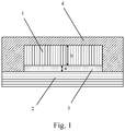
- a chip packaging structure as shown in Fig. 1 , includes: a die 1, a carrier 2, a die attach film 3 and a plastic package body 4.
- the die attach film 3 is disposed on a bottom surface of the die 1, and a thickness of the die attach film 3 is greater than or equal to 40 micrometers.
- the die 1 is disposed on the carrier 2 via the die attach film 3.
- the plastic package body 4 is disposed on the carrier 2 and covers a top surface and a plurality of side surfaces of the die 1.
- Two surfaces of the die attach film 3 can be respectively provided with adhesive, one surface of the die attach film 3 is bonded onto the carrier 2, and the other surface is bonded onto the bottom surface of the die 1, so that the die 1 is disposed on the carrier 2.
- the die attach film 3 can be a soft material, which can have a good buffering effect on the die 1 once the external object impacts the die 1.
- the overall impact resistance, i.e., the strength of the die 1 can be improved by increasing the thickness of the die attach film 3.
- the present chip packaging structure can improve the overall impact resistance, i.e., the strength of the die 1 by increasing the thickness of the die attach film 3. Moreover, there is no need to change the structure of the carrier 2, which saves the expense for making a mold; besides, the packaging structure is simple and the mass production is easy to realize.
- the thickness of the die attach film 3 is greater than or equal to 40 micrometers, so that the strength of the die 1 can be improved by increasing the thickness of the die attach film 3.
- the thickness of the die attach film 3 is smaller than or equal to 150 micrometers, i.e. the thickness of the die attach film 3 is controlled within a range from 40 micrometers to 150 micrometers, not only can the strength of the die 1 be ensured, but also the production difficulty can be reduced, and the packaging yield can be increased.
- a total thickness of the die 1 and the die attach film 3 is equal to a first preset value (as shown in Fig. 1 , the thickness of the die attach film 3 is and the thickness of the die 1 is b, the sum of a and b is equal to the first preset value.
- the first preset value may be set according to the actual requirement.
- the first preset value may be a height of the die and the die attach film in the existing art.
- the thickness b of the die 1 can be correspondingly reduced, so that the total thickness of the chip packaging structure can be constant, thereby avoiding the effect of the increased total thickness of the chip packaging structure on the design or manufacturing of an electronic device using the chip packaging structure.
- the carrier 2 may be a substrate.
- the carrier 2 may be a lead frame. This is not limited in the present embodiment.
- the present chip packaging structure provides a preferable implementation manner of the die attach film 3 and the carrier 2.
- the thickness of the die attach film 3 not only can ensure the strength of the die 1, but also can reduce the production difficulty, thereby improving the packaging yield.
- the total thickness of the chip packaging structure is constant, the effect of the increased total thickness of the chip packaging structure on the design or manufacturing of an electronic device using the chip packaging structure is avoided.
- the chip packaging structure may further include a protection layer 5, as shown in Fig. 2 .
- the protection layer 5 may be disposed on the top surface of the die 1 and coated by the plastic package body 4.
- the protection layer 5 may be of a polyimide material, so that the die 1 can be well protected, and the external impact damage can be better resisted, thereby improving the overall strength.
- the total thickness of a portion of the plastic package body 4 covering the protection layer 5 and the protection layer 5 is equal to a second preset value (as shown in Fig. 2 , the thickness of the protection layer 5 is c, and the thickness of the portion of the plastic package body 4 covering the protection layer 5 is d, the sum of c and d is equal to the second preset value).
- the second preset value may be set according to the actual requirement.
- the second preset value may be a height of a portion of the plastic package body corresponding to the top surface of the die in the chip packaging structure of the existing art.
- the thickness c of the protection layer 5 may be greater than or equal to 1 micrometer, and less than or equal to 20 micrometers.
- the thickness d of the plastic package body 4 above the protection layer 5 can be appropriately reduced, so that the sum of the thickness of the protection layer and the thickness of the plastic package body 4 above the protection layer 5 is equal to the second preset value, i.e. the thickness sum of the protection layer 5 and the plastic package body 4 above the protection layer 5 may be constant, so that the performance of the die 1 is not influenced.
- the die 1 can be well protected by the protection layer 5 and can better resist the external impact damage, thereby improving the overall strength.
- a total height of the protection layer 5 and the plastic package body 4 above the protection layer 5 is constant, so that the performance of the chip is not influenced, and the total packaging thickness is constant.
- the bottom surface of the die 1 is a smooth surface, referring to Fig. 1 .
- the die 1 is ground into a specific thickness during the chip packaging process, which may results in a lot of scratches at the bottom of the die 1, and the scratches are generally the origin of cracks of the die 1. That is, the die 1 is easy to crack when the die 1 is under the external static pressure. Therefore, it may polish the bottom of the die 1 to form a smooth surface, so that the scratches can be effectively decreased, i.e. the crack source is decreased, thereby improving the strength of the die 1.
- the substrate and the die attach film 3 may be made of a high-modulus material, referring to Fig. 1 .
- the modulus of the substrate may be greater than 20GPa, and the modulus of the die attach film 3 may be greater than 4MPa, so that under certain stress effect, the elastic deformation of the substrate and the die attach film 3 can be greatly reduced, i.e. the rigidity of the substrate and the die attach film 3 can be improved.
- the above provides a preferable implementation manner of the substrate and the die attach film 3, so that the rigidity of the substrate and the die attach film 3 can be improved.
- FIG. 3 A chip packaging method which is not in accordance with the invention is as shown in Fig. 3 , which is specifically as follows:
- a plurality of dies to be packaged are generally connected together to form an interconnected die.
- the die attach film can be bonded onto the bottom surface of the interconnected die, then the interconnected die is cut into single dies (at this time, the bottom surface of each single die is provided with the adhesive layer), and the single die is the die of the present disclosure.
- the plurality of single dies are disposed on the carrier (a substrate or a lead frame), and the plurality of single dies are packaged by an injection molding method. Finally the packaged chip is cut to obtain a single chip packaging structure, and the single chip packaging structure is the chip packaging structure of the present disclosure.
- the present method can improve the overall impact resistance, i.e., the strength of the die by increasing the thickness of the die attach film. Moreover, there is no need to change the structure of the carrier, which saves the expense for making a mold; besides, the packaging structure is simple and the mass production is easy to realize.
- figure 3 shows a method corresponding to the chip packaging structure of figure 1 , and the present method can be implemented cooperatively with the chip packaging structure of figure 1 .
- the relevant technical details mentioned in the chip packaging structure are valid in the present method, and in order to reduce duplication, the details are not described herein.
- the relevant technical details mentioned in the present method may also be applied to the chip packaging structure of figure 1 .
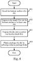
- FIG. 4 A method which improves on the method of figure 3 , and which is in accordance with an embodiment of the invention, is now described.
- the improvement lies in that: in the present method, the bottom surface of the die is ground before the die attach film is disposed on the bottom surface of the die, and the process of the chip packaging method is as shown in Fig. 4 , which is specifically as follows:
- the bottom surface of the die is ground, wherein a total thickness of the ground die and the die attach film is equal to a first preset value.
- the bottom surface of the die may be ground to reduce the height of the die.
- the die may be firstly ground to the height in the existing art and then continuously ground to the height of the present solution, so that the total thickness of the ground die and the die attach film is equal to the first preset value.
- the first preset value can be set according to the actual requirement.
- the first preset value may be a height value of the die and the die attach film in the existing art, that is to say, if the thickness of the die attach film is relative large, the thickness of the die can be correspondingly decreased, so that the total thickness of the chip packaging structure can be constant, thereby avoiding an influence of the increased total thickness of the chip packaging structure on the design or manufacturing of an electronic device using the chip packaging structure.
- the die attach film is disposed on the bottom surface of at least one die. Specifically, two surfaces of the die attach film are respectively provided with the adhesive, the thickness of the die attach film is greater than or equal to 40 micrometers, and less than or equal to 150 micrometers, and the modulus of the die attach film may be greater than 4MPa.
- the die is disposed on the carrier via the die attach film.
- the carrier may be a substrate, and the modulus of the substrate may be greater than 20GPa.
- One surface of the die attach film may be bonded onto the carrier, and the other surface may be bonded onto the bottom surface of the die, so that the die can be disposed on the carrier.
- the carrier may be a lead frame, and is not limited.
- the die is plastic packaged by utilizing the plastic package body.
- the plastic package body is disposed on the carrier and coats a top surface and a plurality of side surfaces of the die to form the chip packaging structure.
- it may grind the bottom surface of the interconnected die when performing grind on the bottom surface of the die.
- the bottom surface of the die is ground before the die attach film is disposed on the die, so that the total thickness of the ground die and the die attach film is equal to the first preset value; therefore, the total thickness of the chip packaging structure is constant, and the influence of the increased total thickness of the chip packaging structure on the design or manufacturing of an electronic device using the chip packaging structure can be avoided. Moreover, by limiting an upper limit value of the thickness of the die attach film, not only can the strength of the chip be ensured, but also the production difficulty can be reduced, and the packaging yield can be increased.
- a further method is improved on the basis of the method of figure 3 .
- the improvement lies in that: a protection layer may be disposed on a top surface of the die before the die attach film is disposed on the bottom surface of the die, and the process of the chip packaging method is as shown in Fig. 5 , which is specifically as follows:
- the present method may also be improved on the basis of the method of figure 3 , i.e. the top surface of the ground die may also be provided with the protection layer.
- the die can be well protected by the protection layer and can better resist the external impact damage, thereby improving the overall strength.
- a total height of the protection layer and the plastic package body above the protection layer is constant, so that the performance of the chip is not influenced, and the total packaging thickness is constant.
- the present method corresponds to the chip packaging structure of figure 2 , and the present method can be implemented cooperatively with the chip packaging structure of figure 2 .
- the relevant technical details mentioned with respect to figure 2 are still valid in the present method, and in order to reduce duplication, the details are not described herein.
- the relevant technical details mentioned in the present method may also be applied to the chip packaging structure of figure 2 .
- a further method is improved on the basis of the method of figure 3 .
- the improvement lies in that: the bottom surface of the die is polished to form the smooth surface before the die attach film is disposed on the bottom surface of the die, and the process of the chip packaging method is as shown in Fig. 6 . which is specifically as follows:
- step 601 the bottom surface of the die is polished to form the smooth surface.
- the die attach film is disposed on the bottom surface of at least one die.
- the thickness of the die attach film is greater than or equal to 40 micrometers, and two surfaces of the die attach film are respectively provided with adhesive.
- the die is disposed on the carrier via the die attach film.
- one surface of the die attach film may be bonded onto the carrier, the other surface is bonded onto the bottom surface of the die.
- the smooth surface of the die faces the die attach film, so that the die can be disposed on the carrier.
- the die is plastic packaged by utilizing the plastic package body.
- the plastic package body is disposed on the carrier and coats the top surface and a plurality of side surfaces of the die to form the chip packaging structure.
- the present method may also be improved on the basis of the method of figure 4 , i.e. the bottom surface of the ground die may also be polished to form the smooth surface.
- the present method can also be improved on the basis of the method of figure 5 , i.e. the bottom surface of the die may also be polished to form the smooth surface after the protection layer is disposed on the top surface of the die.
- the bottom of the die may be polished, so that the bottom surface of the die is the smooth surface, the scratches can be effectively decreased, i.e. the crack sources can be decreased (cracks are likely to occur at the scratches when the die is under the external pressure), thereby improving the strength of the die.
- the present method is a method corresponding to the previously described chip packaging structure in which the bottom surface of the die is a smooth surface, and the present method can be implemented cooperatively with this chip packaging structure.
- the relevant technical details mentioned in respect of this chip packaging structure are still valid in the present method, and in order to reduce duplication, the details are not described herein.
- the relevant technical details mentioned in the present method can also be applied to this chip packaging structure.
- a program to instruct relevant hardware can be completed by adopting a program to instruct relevant hardware, and the program is stored in a storage medium and includes a plurality of instructions enabling one device (may be a single chip microcomputer, a chip and the like) or a processor to execute all or partial steps of the method in each embodiment of the present application.
- the forgoing storage medium includes various mediums capable of storing a program code such as a USB flash disk, a mobile hard disk, a read-only memory (ROM), a random access memory (RAM), a diskette or a compact disk and the like.
Landscapes
- Engineering & Computer Science (AREA)
- Human Computer Interaction (AREA)
- Physics & Mathematics (AREA)
- General Physics & Mathematics (AREA)
- Multimedia (AREA)
- Theoretical Computer Science (AREA)
- Structures Or Materials For Encapsulating Or Coating Semiconductor Devices Or Solid State Devices (AREA)
- Encapsulation Of And Coatings For Semiconductor Or Solid State Devices (AREA)
- Container, Conveyance, Adherence, Positioning, Of Wafer (AREA)
Description
- The present disclosure relates to the packaging technologies, in particular to a chip packaging method.
- A fingerprint module is an important exterior component of an electronic device such as a mobile phone, a tablet computer and the like. Consumers have higher and higher requirements on its structural strength, i.e. the fingerprint module is required to bear certain external force of static pressure and the impact damage action of an external object. In practice, strength of a fingerprint sensor is tested by slowly applying external force onto the fingerprint module through a spherical pressure head, or by dropping a steel ball from a certain height onto the fingerprint module.
- In the process of making an invention of the present disclosure, the inventor(s) found that there are at least the following problems in the existing technologies: existing fingerprint sensors are still difficult to meet the high-strength requirements. They can easily fail in function, and even worse, the chip cracks, under the external force of static pressure and the impact action of an external object.
-
US 2012153508 A1 ,US2005095812 A1 ,US 2013228901 A1 andUS 2005037537 A1 disclose relevant prior art. - The present disclosure describes a chip packaging structure and packaging method, which can improve the overall impact resistance of a chip without changing the structure of a carrier, and save the expense for making a mold; and the packaging structure is simple and easy for mass production. The invention is set out in the appended set of claims.
- Compared with the existing technologies, some aspects of the present disclosure can improve the overall impact resistance of the chip, i.e., improve the strength of the chip, by increasing the thickness of the die attach film. Moreover, there is no need to change the structure of the carrier, the expense for making a mold is saved; besides, the packaging structure is simple, and the mass production is easy to realize.
- A detailed embodiment of the present invention is described below with reference to
figures 1-6 . - In the following, like reference numerals in the drawings represent similar elements; unless otherwise specifically specified, the drawings do not represent the proportion limit.
-
Fig. 1 is a schematic diagram illustrating a chip packaging structure. -
Fig. 2 is a schematic diagram illustrating the chip packaging structure. -
Fig. 3 is a flow chart illustrating a chip packaging method. -
Fig. 4 is a flow chart illustrating a chip packaging method. -
Fig. 5 is a flow chart illustrating a chip packaging method. -
Fig. 6 is a flow chart illustrating a chip packaging method. - A chip packaging structure, as shown in
Fig. 1 , includes: a die 1, acarrier 2, a dieattach film 3 and aplastic package body 4. - Specifically, the die
attach film 3 is disposed on a bottom surface of the die 1, and a thickness of the dieattach film 3 is greater than or equal to 40 micrometers. The die 1 is disposed on thecarrier 2 via the dieattach film 3. Theplastic package body 4 is disposed on thecarrier 2 and covers a top surface and a plurality of side surfaces of thedie 1. - Two surfaces of the die
attach film 3 can be respectively provided with adhesive, one surface of thedie attach film 3 is bonded onto thecarrier 2, and the other surface is bonded onto the bottom surface of thedie 1, so that thedie 1 is disposed on thecarrier 2. In actual practices, when an external object impacts the die 1, a circuit layer of the die 1 is easily damaged, even worse, the whole die 1 cracks, thus in the present embodiment, the dieattach film 3 can be a soft material, which can have a good buffering effect on the die 1 once the external object impacts the die 1. Moreover, the overall impact resistance, i.e., the strength of thedie 1, can be improved by increasing the thickness of thedie attach film 3. - Compared with the existing art, the present chip packaging structure can improve the overall impact resistance, i.e., the strength of the
die 1 by increasing the thickness of thedie attach film 3. Moreover, there is no need to change the structure of thecarrier 2, which saves the expense for making a mold; besides, the packaging structure is simple and the mass production is easy to realize. - In the present invention, the thickness of the
die attach film 3 is greater than or equal to 40 micrometers, so that the strength of thedie 1 can be improved by increasing the thickness of thedie attach film 3. However, if the thickness of thedie attach film 3 is excessively large, thedie 1 is likely to incline when thedie 1 is wired bonded, which increases the production difficulty and decreases the packaging yield. Preferably the thickness of thedie attach film 3 is smaller than or equal to 150 micrometers, i.e. the thickness of thedie attach film 3 is controlled within a range from 40 micrometers to 150 micrometers, not only can the strength of thedie 1 be ensured, but also the production difficulty can be reduced, and the packaging yield can be increased. - A total thickness of the
die 1 and thedie attach film 3 is equal to a first preset value (as shown inFig. 1 , the thickness of thedie attach film 3 is and the thickness of thedie 1 is b, the sum of a and b is equal to the first preset value. The first preset value may be set according to the actual requirement. For example, the first preset value may be a height of the die and the die attach film in the existing art. In other words, if the thickness of thedie attach film 3 is relatively large, the thickness b of thedie 1 can be correspondingly reduced, so that the total thickness of the chip packaging structure can be constant, thereby avoiding the effect of the increased total thickness of the chip packaging structure on the design or manufacturing of an electronic device using the chip packaging structure. - The
carrier 2 may be a substrate. Of course, thecarrier 2 may be a lead frame. This is not limited in the present embodiment. - The present chip packaging structure provides a preferable implementation manner of the die
attach film 3 and thecarrier 2. By limiting the upper limit value of the thickness of thedie attach film 3, not only can ensure the strength of thedie 1, but also can reduce the production difficulty, thereby improving the packaging yield. Moreover, since the total thickness of the chip packaging structure is constant, the effect of the increased total thickness of the chip packaging structure on the design or manufacturing of an electronic device using the chip packaging structure is avoided. - The chip packaging structure may further include a
protection layer 5, as shown inFig. 2 . - Specifically, the
protection layer 5 may be disposed on the top surface of thedie 1 and coated by theplastic package body 4. Preferably, theprotection layer 5 may be of a polyimide material, so that thedie 1 can be well protected, and the external impact damage can be better resisted, thereby improving the overall strength. - The total thickness of a portion of the
plastic package body 4 covering theprotection layer 5 and theprotection layer 5 is equal to a second preset value (as shown inFig. 2 , the thickness of theprotection layer 5 is c, and the thickness of the portion of theplastic package body 4 covering theprotection layer 5 is d, the sum of c and d is equal to the second preset value). Specifically, the second preset value may be set according to the actual requirement. For example, the second preset value may be a height of a portion of the plastic package body corresponding to the top surface of the die in the chip packaging structure of the existing art. The thickness c of theprotection layer 5 may be greater than or equal to 1 micrometer, and less than or equal to 20 micrometers. If the thickness c of theprotection layer 5 is relative large, the thickness d of theplastic package body 4 above theprotection layer 5 can be appropriately reduced, so that the sum of the thickness of the protection layer and the thickness of theplastic package body 4 above theprotection layer 5 is equal to the second preset value, i.e. the thickness sum of theprotection layer 5 and theplastic package body 4 above theprotection layer 5 may be constant, so that the performance of thedie 1 is not influenced. - The
die 1 can be well protected by theprotection layer 5 and can better resist the external impact damage, thereby improving the overall strength. By limiting the total thickness of the portion of theplastic package body 4 covering theprotection layer 5 and theprotection layer 5, a total height of theprotection layer 5 and theplastic package body 4 above theprotection layer 5 is constant, so that the performance of the chip is not influenced, and the total packaging thickness is constant. - In a further improvement, the bottom surface of the
die 1 is a smooth surface, referring toFig. 1 . - Specifically, the
die 1 is ground into a specific thickness during the chip packaging process, which may results in a lot of scratches at the bottom of thedie 1, and the scratches are generally the origin of cracks of thedie 1. That is, thedie 1 is easy to crack when thedie 1 is under the external static pressure. Therefore, it may polish the bottom of thedie 1 to form a smooth surface, so that the scratches can be effectively decreased, i.e. the crack source is decreased, thereby improving the strength of thedie 1. - The above-described further improvement effectively decreases the scratches, i.e. the crack source (cracks are likely to occur at the scratches when the die is under the external pressure), thereby improving the strength of the
die 1. - The substrate and the die
attach film 3 may be made of a high-modulus material, referring toFig. 1 . - Specifically, the modulus of the substrate may be greater than 20GPa, and the modulus of the die
attach film 3 may be greater than 4MPa, so that under certain stress effect, the elastic deformation of the substrate and the dieattach film 3 can be greatly reduced, i.e. the rigidity of the substrate and the dieattach film 3 can be improved. - The above provides a preferable implementation manner of the substrate and the
die attach film 3, so that the rigidity of the substrate and thedie attach film 3 can be improved. - A chip packaging method which is not in accordance with the invention is as shown in
Fig. 3 , which is specifically as follows: - In
step 301, a die attach film is disposed on a bottom surface of at least one die. Specifically, a thickness of the die attach film is greater than or equal to 40 micrometers, and two surfaces of the die attach film are respectively provided with adhesive. - In
step 302, the die is disposed on a carrier via the die attach film. Specifically, one surface of the die attach film is bonded onto the carrier, and the other surface is bonded onto the bottom surface of the die, so that the die can be disposed on the carrier. - In
step 303, the die is plastic packaged by utilizing a plastic package body. The plastic package body is disposed on the carrier and coats a top surface and a plurality of side surfaces of the die to form a chip packaging structure. - A plurality of dies to be packaged are generally connected together to form an interconnected die. The die attach film can be bonded onto the bottom surface of the interconnected die, then the interconnected die is cut into single dies (at this time, the bottom surface of each single die is provided with the adhesive layer), and the single die is the die of the present disclosure. Then, the plurality of single dies are disposed on the carrier (a substrate or a lead frame), and the plurality of single dies are packaged by an injection molding method. Finally the packaged chip is cut to obtain a single chip packaging structure, and the single chip packaging structure is the chip packaging structure of the present disclosure.
- Compared with the existing art, the present method can improve the overall impact resistance, i.e., the strength of the die by increasing the thickness of the die attach film. Moreover, there is no need to change the structure of the carrier, which saves the expense for making a mold; besides, the packaging structure is simple and the mass production is easy to realize.
- It is not difficult to find that
figure 3 shows a method corresponding to the chip packaging structure offigure 1 , and the present method can be implemented cooperatively with the chip packaging structure offigure 1 . The relevant technical details mentioned in the chip packaging structure are valid in the present method, and in order to reduce duplication, the details are not described herein. Correspondingly, the relevant technical details mentioned in the present method may also be applied to the chip packaging structure offigure 1 . - A method which improves on the method of
figure 3 , and which is in accordance with an embodiment of the invention, is now described. The improvement lies in that: in the present method, the bottom surface of the die is ground before the die attach film is disposed on the bottom surface of the die, and the process of the chip packaging method is as shown inFig. 4 , which is specifically as follows: - In
step 401, the bottom surface of the die is ground, wherein a total thickness of the ground die and the die attach film is equal to a first preset value. Specifically, the bottom surface of the die may be ground to reduce the height of the die. The die may be firstly ground to the height in the existing art and then continuously ground to the height of the present solution, so that the total thickness of the ground die and the die attach film is equal to the first preset value. The first preset value can be set according to the actual requirement. For example, the first preset value may be a height value of the die and the die attach film in the existing art, that is to say, if the thickness of the die attach film is relative large, the thickness of the die can be correspondingly decreased, so that the total thickness of the chip packaging structure can be constant, thereby avoiding an influence of the increased total thickness of the chip packaging structure on the design or manufacturing of an electronic device using the chip packaging structure. - In
step 402, the die attach film is disposed on the bottom surface of at least one die. Specifically, two surfaces of the die attach film are respectively provided with the adhesive, the thickness of the die attach film is greater than or equal to 40 micrometers, and less than or equal to 150 micrometers, and the modulus of the die attach film may be greater than 4MPa. - In
step 403, the die is disposed on the carrier via the die attach film. Specifically, the carrier may be a substrate, and the modulus of the substrate may be greater than 20GPa. One surface of the die attach film may be bonded onto the carrier, and the other surface may be bonded onto the bottom surface of the die, so that the die can be disposed on the carrier. - The carrier may be a lead frame, and is not limited.
- In
step 404, the die is plastic packaged by utilizing the plastic package body. The plastic package body is disposed on the carrier and coats a top surface and a plurality of side surfaces of the die to form the chip packaging structure. - In the present method, it may grind the bottom surface of the interconnected die when performing grind on the bottom surface of the die.
- The bottom surface of the die is ground before the die attach film is disposed on the die, so that the total thickness of the ground die and the die attach film is equal to the first preset value; therefore, the total thickness of the chip packaging structure is constant, and the influence of the increased total thickness of the chip packaging structure on the design or manufacturing of an electronic device using the chip packaging structure can be avoided. Moreover, by limiting an upper limit value of the thickness of the die attach film, not only can the strength of the chip be ensured, but also the production difficulty can be reduced, and the packaging yield can be increased.
- A further method is improved on the basis of the method of
figure 3 . The improvement lies in that: a protection layer may be disposed on a top surface of the die before the die attach film is disposed on the bottom surface of the die, and the process of the chip packaging method is as shown inFig. 5 , which is specifically as follows: - In
step 501, the top surface of the die is provided with the protection layer. Specifically, the protection layer can be disposed on the top surface of the die by a spray coating method or a spin coating method; the protection layer may be of a polyimide material, so that the die can be well protected and can better resist the external impact damage, thereby improving the overall strength. - In
step 502, the die attach film is disposed on the bottom surface of at least one die. Specifically, the thickness of the die attach film is greater than or equal to 40 micrometers, and two surfaces of the die attach film are respectively provided with adhesive. - In
step 503, the die is disposed on the carrier via the die attach film. Specifically, one surface of the die attach film is bonded onto the carrier, and the other surface is bonded onto the bottom surface of the die, so that the die can be disposed on the carrier. - In
step 504, the die is plastic packaged by utilizing the plastic package body. The plastic package body is disposed on the carrier, and coats the top surface and a plurality of side surfaces of the die to form the chip packaging structure. Specifically, the total thickness of the portion of the plastic package body covering the protection layer and the protection layer is equal to a second preset value. The second preset value may be set according to the actual requirement. For example, the second preset value may be a height value of the portion of the plastic package body corresponding to the top surface of the die in the chip packaging structure of the existing art. Preferably, the thickness of the protection layer may be greater than or equal to 1 micrometer, and less than or equal to 20 micrometers. In this case, if the thickness of the protection layer is relative large, the thickness of the plastic package body above the protection layer can be appropriately reduced, so that a sum of the thickness of the protection layer and the thickness of the plastic package body above the protection layer is equal to the second preset value, i.e. the sum of the thickness of the protection layer and the thickness of the plastic package body above the protection layer may be constant, and the performance of the chip is not influenced. - It shall be noted that the present method may also be improved on the basis of the method of
figure 3 , i.e. the top surface of the ground die may also be provided with the protection layer. - In the present method, the die can be well protected by the protection layer and can better resist the external impact damage, thereby improving the overall strength. By limiting the total thickness of the portion of the plastic package body covering the protection layer and the protection layer, a total height of the protection layer and the plastic package body above the protection layer is constant, so that the performance of the chip is not influenced, and the total packaging thickness is constant.
- The present method corresponds to the chip packaging structure of
figure 2 , and the present method can be implemented cooperatively with the chip packaging structure offigure 2 . The relevant technical details mentioned with respect tofigure 2 are still valid in the present method, and in order to reduce duplication, the details are not described herein. Correspondingly, the relevant technical details mentioned in the present method may also be applied to the chip packaging structure offigure 2 . - A further method is improved on the basis of the method of
figure 3 . The improvement lies in that: the bottom surface of the die is polished to form the smooth surface before the die attach film is disposed on the bottom surface of the die, and the process of the chip packaging method is as shown inFig. 6 . which is specifically as follows: - In
step 601, the bottom surface of the die is polished to form the smooth surface. - In
step 602, the die attach film is disposed on the bottom surface of at least one die. Specifically, the thickness of the die attach film is greater than or equal to 40 micrometers, and two surfaces of the die attach film are respectively provided with adhesive. - In
step 603, the die is disposed on the carrier via the die attach film. Specifically, one surface of the die attach film may be bonded onto the carrier, the other surface is bonded onto the bottom surface of the die. The smooth surface of the die faces the die attach film, so that the die can be disposed on the carrier. - In
step 604, the die is plastic packaged by utilizing the plastic package body. The plastic package body is disposed on the carrier and coats the top surface and a plurality of side surfaces of the die to form the chip packaging structure. - It shall be noted that the present method may also be improved on the basis of the method of
figure 4 , i.e. the bottom surface of the ground die may also be polished to form the smooth surface. Of course, the present method can also be improved on the basis of the method offigure 5 , i.e. the bottom surface of the die may also be polished to form the smooth surface after the protection layer is disposed on the top surface of the die. - In the present method, the bottom of the die may be polished, so that the bottom surface of the die is the smooth surface, the scratches can be effectively decreased, i.e. the crack sources can be decreased (cracks are likely to occur at the scratches when the die is under the external pressure), thereby improving the strength of the die.
- The present method is a method corresponding to the previously described chip packaging structure in which the bottom surface of the die is a smooth surface, and the present method can be implemented cooperatively with this chip packaging structure. The relevant technical details mentioned in respect of this chip packaging structure are still valid in the present method, and in order to reduce duplication, the details are not described herein. Correspondingly, the relevant technical details mentioned in the present method can also be applied to this chip packaging structure.
- Those skilled in the art may understand that all or partial steps in the method of the above embodiments can be completed by adopting a program to instruct relevant hardware, and the program is stored in a storage medium and includes a plurality of instructions enabling one device (may be a single chip microcomputer, a chip and the like) or a processor to execute all or partial steps of the method in each embodiment of the present application. The forgoing storage medium includes various mediums capable of storing a program code such as a USB flash disk, a mobile hard disk, a read-only memory (ROM), a random access memory (RAM), a diskette or a compact disk and the like.
Claims (6)
- A chip packaging method for forming a chip packaging structure comprising a die (1), a carrier (2), a die attach film (3) and a plastic package body (4), the die attach film being disposed on a bottom surface of the die, and the thickness of the die attach film being greater than or equal to 40 micrometers, the die being disposed on the carrier via the die attach film and the plastic package body being disposed on the carrier body and coating a top surface and a plurality of side surfaces of the die, wherein the total thickness of the die and the die attach film is equal to a first preset value, the first preset value being a constant value, the method comprising:disposing a die attach film on a bottom surface of a die, wherein the thickness of the die attach film is greater than or equal to 40 micrometers;disposing the die on a carrier via the die attach film; andplastic packaging the die by utilizing a plastic package body, wherein the plastic package body is disposed on the carrier and coats a top surface and a plurality of side surfaces of the die to form a chip packaging structure;wherein before the die attach film is disposed on the bottom surface of the die, the chip packaging method further comprises:
grinding the bottom surface of the die to reduce the thickness of the die until the total thickness of the ground die and the die attach film equals the first constant preset value . - The chip packaging method according to claim 1, wherein the thickness of the die attach film is less than or equal to 150 micrometers.
- The chip packaging method according to claim 1 or 2, wherein before the die attach film is disposed on the bottom surface of the die, the chip packaging method further comprises:
polishing the bottom surface of the die to form a smooth surface, wherein the smooth surface faces the die attach film. - The chip packaging method according to any one of claims 1 to 3, wherein before the die attach film is disposed on the bottom surface of the die, the chip packaging method further comprises:
disposing a protection layer (5) on the top surface of the die - The chip packaging method according to claim 4, wherein the total thickness of a portion of the plastic package body covering the protection layer and the protection layer is equal to a second preset value; wherein the second preset value is a constant value, wherein the method further comprises reducing the thickness of the portion of the plastic package body covering the protection layer until the total thickness of the portion of the plastic package body covering the protection layer and the protection layer equals the second constant preset value.
- The chip packaging method according to claim 4 or 5, wherein the protection layer is disposed on the top surface of the die of the protection layer by a spray coating method or a spin coating method.
Applications Claiming Priority (1)
| Application Number | Priority Date | Filing Date | Title |
|---|---|---|---|
| PCT/CN2017/072710 WO2018137224A1 (en) | 2017-01-25 | 2017-01-25 | Wafer encapsulation structure and encapsulation method |
Publications (3)
| Publication Number | Publication Date |
|---|---|
| EP3435410A1 EP3435410A1 (en) | 2019-01-30 |
| EP3435410A4 EP3435410A4 (en) | 2019-05-29 |
| EP3435410B1 true EP3435410B1 (en) | 2021-07-07 |
Family
ID=62977945
Family Applications (1)
| Application Number | Title | Priority Date | Filing Date |
|---|---|---|---|
| EP17894547.3A Active EP3435410B1 (en) | 2017-01-25 | 2017-01-25 | Chip encapsulation structure and encapsulation method |
Country Status (4)
| Country | Link |
|---|---|
| US (1) | US10727196B2 (en) |
| EP (1) | EP3435410B1 (en) |
| CN (1) | CN108780782A (en) |
| WO (1) | WO2018137224A1 (en) |
Family Cites Families (11)
| Publication number | Priority date | Publication date | Assignee | Title |
|---|---|---|---|---|
| KR100517075B1 (en) * | 2003-08-11 | 2005-09-26 | 삼성전자주식회사 | Method for manufacturing semiconductor device |
| US6940181B2 (en) * | 2003-10-21 | 2005-09-06 | Micron Technology, Inc. | Thinned, strengthened semiconductor substrates and packages including same |
| JP4717051B2 (en) * | 2007-11-08 | 2011-07-06 | 日東電工株式会社 | Dicing die bond film |
| JP2010171402A (en) * | 2008-12-24 | 2010-08-05 | Nitto Denko Corp | Thermosetting die-bonding film |
| US8710682B2 (en) * | 2009-09-03 | 2014-04-29 | Designer Molecules Inc, Inc. | Materials and methods for stress reduction in semiconductor wafer passivation layers |
| JP2013045863A (en) * | 2011-08-24 | 2013-03-04 | Elpida Memory Inc | Semiconductor device and manufacturing method of the same |
| CN102522383B (en) * | 2011-12-31 | 2015-08-12 | 天水华天科技股份有限公司 | A kind of IC chip stacked packaging piece with two-ring-arrangement center routing and production method thereof |
| CN102543931B (en) * | 2011-12-31 | 2015-06-17 | 天水华天科技股份有限公司 | Preparation method for center-wiring double-circle-arrangement single-IC (integrated circuit) chip packaging piece |
| CN105097722B (en) * | 2014-05-05 | 2019-12-13 | 清华大学 | Semiconductor packaging structure and packaging method |
| KR102401764B1 (en) * | 2014-12-31 | 2022-05-26 | 하나 마이크론(주) | electron device and method of manufacturing the same |
| CN106158780A (en) * | 2016-08-11 | 2016-11-23 | 华天科技(西安)有限公司 | The encapsulating structure of a kind of DAF film parcel fingerprint sensor and manufacture method thereof |
-
2017
- 2017-01-25 CN CN201780005876.7A patent/CN108780782A/en active Pending
- 2017-01-25 EP EP17894547.3A patent/EP3435410B1/en active Active
- 2017-01-25 WO PCT/CN2017/072710 patent/WO2018137224A1/en not_active Ceased
-
2018
- 2018-10-25 US US16/170,847 patent/US10727196B2/en active Active
Non-Patent Citations (1)
| Title |
|---|
| None * |
Also Published As
| Publication number | Publication date |
|---|---|
| US10727196B2 (en) | 2020-07-28 |
| WO2018137224A1 (en) | 2018-08-02 |
| US20190067236A1 (en) | 2019-02-28 |
| EP3435410A1 (en) | 2019-01-30 |
| EP3435410A4 (en) | 2019-05-29 |
| CN108780782A (en) | 2018-11-09 |
Similar Documents
| Publication | Publication Date | Title |
|---|---|---|
| US11658154B2 (en) | Memory devices with controllers under memory packages and associated systems and methods | |
| TWI594396B (en) | Vertical stacking of system-level packages and methods of forming a vertically stacked system-in-package | |
| US10770445B2 (en) | Methods of fabricating semiconductor packages including reinforcement top die | |
| US10256208B2 (en) | Overlapping stacked die package with vertical columns | |
| US20160225707A1 (en) | Electronic assembly that includes stacked electronic devices | |
| US9542598B2 (en) | Package structure and fabrication method thereof | |
| US11480999B2 (en) | Mobile communication device cover glass | |
| CN204011397U (en) | Capacitive fingerprint sensor encapsulating structure | |
| US10727196B2 (en) | Chip packaging structure and packaging method | |
| CN105529308A (en) | Fingerprint chip package structure with cushion block employing underfill technology and manufacturing method | |
| KR101633398B1 (en) | A land grid array package capable of decreasing a height difference between land and solder resist | |
| CN205264683U (en) | Cushion adds underfill's fingerprint chip packaging structure | |
| WO2019066960A1 (en) | Stacked die semiconductor package spacer die | |
| US20160192500A1 (en) | Electronic Devices and Methods of Manufacturing Electronic Devices | |
| US10559539B2 (en) | Wafer level packages, semiconductor device units, and methods of fabricating the same | |
| CN209071313U (en) | Chip package structure with six face formula protective layers | |
| US20130302589A1 (en) | Soft pad for vehicle and manufacturing method thereof | |
| CN206610804U (en) | Chip package structure | |
| TWI730812B (en) | Fingerprint sensing chip module for a smart card and packaging method of the same | |
| CN205303442U (en) | Fingerprint identification chip package structure based on high roughness base plate | |
| CN207868188U (en) | A kind of fingerprint recognition chip-packaging structure | |
| KR101893211B1 (en) | Manufacturing method of grinded fingerprint sensor package by strip type | |
| CN210403666U (en) | Foil card | |
| CN116013872A (en) | Packaging structure, packaging method and electronic equipment of a fingerprint identification chip | |
| CN107749400A (en) | A kind of fingerprint recognition chip-packaging structure and method for packing |
Legal Events
| Date | Code | Title | Description |
|---|---|---|---|
| STAA | Information on the status of an ep patent application or granted ep patent |
Free format text: STATUS: THE INTERNATIONAL PUBLICATION HAS BEEN MADE |
|
| PUAI | Public reference made under article 153(3) epc to a published international application that has entered the european phase |
Free format text: ORIGINAL CODE: 0009012 |
|
| STAA | Information on the status of an ep patent application or granted ep patent |
Free format text: STATUS: REQUEST FOR EXAMINATION WAS MADE |
|
| 17P | Request for examination filed |
Effective date: 20181025 |
|
| AK | Designated contracting states |
Kind code of ref document: A1 Designated state(s): AL AT BE BG CH CY CZ DE DK EE ES FI FR GB GR HR HU IE IS IT LI LT LU LV MC MK MT NL NO PL PT RO RS SE SI SK SM TR |
|
| AX | Request for extension of the european patent |
Extension state: BA ME |
|
| A4 | Supplementary search report drawn up and despatched |
Effective date: 20190502 |
|
| RIC1 | Information provided on ipc code assigned before grant |
Ipc: H01L 23/00 20060101ALI20190425BHEP Ipc: H01L 21/56 20060101ALI20190425BHEP Ipc: H01L 23/31 20060101AFI20190425BHEP |
|
| DAV | Request for validation of the european patent (deleted) | ||
| DAX | Request for extension of the european patent (deleted) | ||
| STAA | Information on the status of an ep patent application or granted ep patent |
Free format text: STATUS: EXAMINATION IS IN PROGRESS |
|
| 17Q | First examination report despatched |
Effective date: 20201007 |
|
| GRAP | Despatch of communication of intention to grant a patent |
Free format text: ORIGINAL CODE: EPIDOSNIGR1 |
|
| STAA | Information on the status of an ep patent application or granted ep patent |
Free format text: STATUS: GRANT OF PATENT IS INTENDED |
|
| RIC1 | Information provided on ipc code assigned before grant |
Ipc: H01L 21/56 20060101ALI20210217BHEP Ipc: H01L 23/00 20060101ALI20210217BHEP Ipc: G06K 9/00 20060101ALI20210217BHEP Ipc: H01L 23/31 20060101AFI20210217BHEP |
|
| INTG | Intention to grant announced |
Effective date: 20210319 |
|
| RIN1 | Information on inventor provided before grant (corrected) |
Inventor name: LUO, JUNPING |
|
| GRAS | Grant fee paid |
Free format text: ORIGINAL CODE: EPIDOSNIGR3 |
|
| GRAA | (expected) grant |
Free format text: ORIGINAL CODE: 0009210 |
|
| STAA | Information on the status of an ep patent application or granted ep patent |
Free format text: STATUS: THE PATENT HAS BEEN GRANTED |
|
| AK | Designated contracting states |
Kind code of ref document: B1 Designated state(s): AL AT BE BG CH CY CZ DE DK EE ES FI FR GB GR HR HU IE IS IT LI LT LU LV MC MK MT NL NO PL PT RO RS SE SI SK SM TR |
|
| REG | Reference to a national code |
Ref country code: GB Ref legal event code: FG4D |
|
| REG | Reference to a national code |
Ref country code: AT Ref legal event code: REF Ref document number: 1409412 Country of ref document: AT Kind code of ref document: T Effective date: 20210715 |
|
| REG | Reference to a national code |
Ref country code: DE Ref legal event code: R096 Ref document number: 602017041916 Country of ref document: DE |
|
| REG | Reference to a national code |
Ref country code: IE Ref legal event code: FG4D |
|
| REG | Reference to a national code |
Ref country code: LT Ref legal event code: MG9D |
|
| REG | Reference to a national code |
Ref country code: NL Ref legal event code: MP Effective date: 20210707 |
|
| REG | Reference to a national code |
Ref country code: AT Ref legal event code: MK05 Ref document number: 1409412 Country of ref document: AT Kind code of ref document: T Effective date: 20210707 |
|
| PG25 | Lapsed in a contracting state [announced via postgrant information from national office to epo] |
Ref country code: SE Free format text: LAPSE BECAUSE OF FAILURE TO SUBMIT A TRANSLATION OF THE DESCRIPTION OR TO PAY THE FEE WITHIN THE PRESCRIBED TIME-LIMIT Effective date: 20210707 Ref country code: RS Free format text: LAPSE BECAUSE OF FAILURE TO SUBMIT A TRANSLATION OF THE DESCRIPTION OR TO PAY THE FEE WITHIN THE PRESCRIBED TIME-LIMIT Effective date: 20210707 Ref country code: HR Free format text: LAPSE BECAUSE OF FAILURE TO SUBMIT A TRANSLATION OF THE DESCRIPTION OR TO PAY THE FEE WITHIN THE PRESCRIBED TIME-LIMIT Effective date: 20210707 Ref country code: ES Free format text: LAPSE BECAUSE OF FAILURE TO SUBMIT A TRANSLATION OF THE DESCRIPTION OR TO PAY THE FEE WITHIN THE PRESCRIBED TIME-LIMIT Effective date: 20210707 Ref country code: FI Free format text: LAPSE BECAUSE OF FAILURE TO SUBMIT A TRANSLATION OF THE DESCRIPTION OR TO PAY THE FEE WITHIN THE PRESCRIBED TIME-LIMIT Effective date: 20210707 Ref country code: NL Free format text: LAPSE BECAUSE OF FAILURE TO SUBMIT A TRANSLATION OF THE DESCRIPTION OR TO PAY THE FEE WITHIN THE PRESCRIBED TIME-LIMIT Effective date: 20210707 Ref country code: NO Free format text: LAPSE BECAUSE OF FAILURE TO SUBMIT A TRANSLATION OF THE DESCRIPTION OR TO PAY THE FEE WITHIN THE PRESCRIBED TIME-LIMIT Effective date: 20211007 Ref country code: PT Free format text: LAPSE BECAUSE OF FAILURE TO SUBMIT A TRANSLATION OF THE DESCRIPTION OR TO PAY THE FEE WITHIN THE PRESCRIBED TIME-LIMIT Effective date: 20211108 Ref country code: AT Free format text: LAPSE BECAUSE OF FAILURE TO SUBMIT A TRANSLATION OF THE DESCRIPTION OR TO PAY THE FEE WITHIN THE PRESCRIBED TIME-LIMIT Effective date: 20210707 Ref country code: BG Free format text: LAPSE BECAUSE OF FAILURE TO SUBMIT A TRANSLATION OF THE DESCRIPTION OR TO PAY THE FEE WITHIN THE PRESCRIBED TIME-LIMIT Effective date: 20211007 Ref country code: LT Free format text: LAPSE BECAUSE OF FAILURE TO SUBMIT A TRANSLATION OF THE DESCRIPTION OR TO PAY THE FEE WITHIN THE PRESCRIBED TIME-LIMIT Effective date: 20210707 |
|
| PG25 | Lapsed in a contracting state [announced via postgrant information from national office to epo] |
Ref country code: PL Free format text: LAPSE BECAUSE OF FAILURE TO SUBMIT A TRANSLATION OF THE DESCRIPTION OR TO PAY THE FEE WITHIN THE PRESCRIBED TIME-LIMIT Effective date: 20210707 Ref country code: LV Free format text: LAPSE BECAUSE OF FAILURE TO SUBMIT A TRANSLATION OF THE DESCRIPTION OR TO PAY THE FEE WITHIN THE PRESCRIBED TIME-LIMIT Effective date: 20210707 Ref country code: GR Free format text: LAPSE BECAUSE OF FAILURE TO SUBMIT A TRANSLATION OF THE DESCRIPTION OR TO PAY THE FEE WITHIN THE PRESCRIBED TIME-LIMIT Effective date: 20211008 |
|
| REG | Reference to a national code |
Ref country code: DE Ref legal event code: R097 Ref document number: 602017041916 Country of ref document: DE |
|
| PG25 | Lapsed in a contracting state [announced via postgrant information from national office to epo] |
Ref country code: DK Free format text: LAPSE BECAUSE OF FAILURE TO SUBMIT A TRANSLATION OF THE DESCRIPTION OR TO PAY THE FEE WITHIN THE PRESCRIBED TIME-LIMIT Effective date: 20210707 |
|
| PLBE | No opposition filed within time limit |
Free format text: ORIGINAL CODE: 0009261 |
|
| STAA | Information on the status of an ep patent application or granted ep patent |
Free format text: STATUS: NO OPPOSITION FILED WITHIN TIME LIMIT |
|
| PG25 | Lapsed in a contracting state [announced via postgrant information from national office to epo] |
Ref country code: SM Free format text: LAPSE BECAUSE OF FAILURE TO SUBMIT A TRANSLATION OF THE DESCRIPTION OR TO PAY THE FEE WITHIN THE PRESCRIBED TIME-LIMIT Effective date: 20210707 Ref country code: SK Free format text: LAPSE BECAUSE OF FAILURE TO SUBMIT A TRANSLATION OF THE DESCRIPTION OR TO PAY THE FEE WITHIN THE PRESCRIBED TIME-LIMIT Effective date: 20210707 Ref country code: RO Free format text: LAPSE BECAUSE OF FAILURE TO SUBMIT A TRANSLATION OF THE DESCRIPTION OR TO PAY THE FEE WITHIN THE PRESCRIBED TIME-LIMIT Effective date: 20210707 Ref country code: EE Free format text: LAPSE BECAUSE OF FAILURE TO SUBMIT A TRANSLATION OF THE DESCRIPTION OR TO PAY THE FEE WITHIN THE PRESCRIBED TIME-LIMIT Effective date: 20210707 Ref country code: CZ Free format text: LAPSE BECAUSE OF FAILURE TO SUBMIT A TRANSLATION OF THE DESCRIPTION OR TO PAY THE FEE WITHIN THE PRESCRIBED TIME-LIMIT Effective date: 20210707 Ref country code: AL Free format text: LAPSE BECAUSE OF FAILURE TO SUBMIT A TRANSLATION OF THE DESCRIPTION OR TO PAY THE FEE WITHIN THE PRESCRIBED TIME-LIMIT Effective date: 20210707 |
|
| 26N | No opposition filed |
Effective date: 20220408 |
|
| PG25 | Lapsed in a contracting state [announced via postgrant information from national office to epo] |
Ref country code: IT Free format text: LAPSE BECAUSE OF FAILURE TO SUBMIT A TRANSLATION OF THE DESCRIPTION OR TO PAY THE FEE WITHIN THE PRESCRIBED TIME-LIMIT Effective date: 20210707 |
|
| PG25 | Lapsed in a contracting state [announced via postgrant information from national office to epo] |
Ref country code: MC Free format text: LAPSE BECAUSE OF FAILURE TO SUBMIT A TRANSLATION OF THE DESCRIPTION OR TO PAY THE FEE WITHIN THE PRESCRIBED TIME-LIMIT Effective date: 20210707 |
|
| REG | Reference to a national code |
Ref country code: CH Ref legal event code: PL |
|
| REG | Reference to a national code |
Ref country code: BE Ref legal event code: MM Effective date: 20220131 |
|
| PG25 | Lapsed in a contracting state [announced via postgrant information from national office to epo] |
Ref country code: LU Free format text: LAPSE BECAUSE OF NON-PAYMENT OF DUE FEES Effective date: 20220125 |
|
| PG25 | Lapsed in a contracting state [announced via postgrant information from national office to epo] |
Ref country code: FR Free format text: LAPSE BECAUSE OF NON-PAYMENT OF DUE FEES Effective date: 20220131 Ref country code: BE Free format text: LAPSE BECAUSE OF NON-PAYMENT OF DUE FEES Effective date: 20220131 |
|
| PG25 | Lapsed in a contracting state [announced via postgrant information from national office to epo] |
Ref country code: LI Free format text: LAPSE BECAUSE OF NON-PAYMENT OF DUE FEES Effective date: 20220131 Ref country code: CH Free format text: LAPSE BECAUSE OF NON-PAYMENT OF DUE FEES Effective date: 20220131 |
|
| PG25 | Lapsed in a contracting state [announced via postgrant information from national office to epo] |
Ref country code: IE Free format text: LAPSE BECAUSE OF NON-PAYMENT OF DUE FEES Effective date: 20220125 |
|
| PG25 | Lapsed in a contracting state [announced via postgrant information from national office to epo] |
Ref country code: HU Free format text: LAPSE BECAUSE OF FAILURE TO SUBMIT A TRANSLATION OF THE DESCRIPTION OR TO PAY THE FEE WITHIN THE PRESCRIBED TIME-LIMIT; INVALID AB INITIO Effective date: 20170125 |
|
| PG25 | Lapsed in a contracting state [announced via postgrant information from national office to epo] |
Ref country code: MK Free format text: LAPSE BECAUSE OF FAILURE TO SUBMIT A TRANSLATION OF THE DESCRIPTION OR TO PAY THE FEE WITHIN THE PRESCRIBED TIME-LIMIT Effective date: 20210707 Ref country code: CY Free format text: LAPSE BECAUSE OF FAILURE TO SUBMIT A TRANSLATION OF THE DESCRIPTION OR TO PAY THE FEE WITHIN THE PRESCRIBED TIME-LIMIT Effective date: 20210707 |
|
| PG25 | Lapsed in a contracting state [announced via postgrant information from national office to epo] |
Ref country code: TR Free format text: LAPSE BECAUSE OF FAILURE TO SUBMIT A TRANSLATION OF THE DESCRIPTION OR TO PAY THE FEE WITHIN THE PRESCRIBED TIME-LIMIT Effective date: 20210707 |
|
| PG25 | Lapsed in a contracting state [announced via postgrant information from national office to epo] |
Ref country code: MT Free format text: LAPSE BECAUSE OF FAILURE TO SUBMIT A TRANSLATION OF THE DESCRIPTION OR TO PAY THE FEE WITHIN THE PRESCRIBED TIME-LIMIT Effective date: 20210707 |
|
| REG | Reference to a national code |
Ref country code: DE Ref legal event code: R079 Ref document number: 602017041916 Country of ref document: DE Free format text: PREVIOUS MAIN CLASS: H01L0023310000 Ipc: H10W0074100000 |
|
| PGFP | Annual fee paid to national office [announced via postgrant information from national office to epo] |
Ref country code: GB Payment date: 20260128 Year of fee payment: 10 |
|
| PGFP | Annual fee paid to national office [announced via postgrant information from national office to epo] |
Ref country code: DE Payment date: 20260128 Year of fee payment: 10 |