EP3435409A1 - Method for measuring resistivity of silicon wafers - Google Patents
Method for measuring resistivity of silicon wafers Download PDFInfo
- Publication number
- EP3435409A1 EP3435409A1 EP18177257.5A EP18177257A EP3435409A1 EP 3435409 A1 EP3435409 A1 EP 3435409A1 EP 18177257 A EP18177257 A EP 18177257A EP 3435409 A1 EP3435409 A1 EP 3435409A1
- Authority
- EP
- European Patent Office
- Prior art keywords
- resistivity
- concentration
- wafers
- thermal donors
- vertical
- Prior art date
- Legal status (The legal status is an assumption and is not a legal conclusion. Google has not performed a legal analysis and makes no representation as to the accuracy of the status listed.)
- Pending
Links
Images


Classifications
-
- G—PHYSICS
- G01—MEASURING; TESTING
- G01R—MEASURING ELECTRIC VARIABLES; MEASURING MAGNETIC VARIABLES
- G01R27/00—Arrangements for measuring resistance, reactance, impedance, or electric characteristics derived therefrom
- G01R27/02—Measuring real or complex resistance, reactance, impedance, or other two-pole characteristics derived therefrom, e.g. time constant
-
- H—ELECTRICITY
- H01—ELECTRIC ELEMENTS
- H01L—SEMICONDUCTOR DEVICES NOT COVERED BY CLASS H10
- H01L22/00—Testing or measuring during manufacture or treatment; Reliability measurements, i.e. testing of parts without further processing to modify the parts as such; Structural arrangements therefor
- H01L22/10—Measuring as part of the manufacturing process
- H01L22/14—Measuring as part of the manufacturing process for electrical parameters, e.g. resistance, deep-levels, CV, diffusions by electrical means
-
- G—PHYSICS
- G01—MEASURING; TESTING
- G01N—INVESTIGATING OR ANALYSING MATERIALS BY DETERMINING THEIR CHEMICAL OR PHYSICAL PROPERTIES
- G01N27/00—Investigating or analysing materials by the use of electric, electrochemical, or magnetic means
- G01N27/02—Investigating or analysing materials by the use of electric, electrochemical, or magnetic means by investigating impedance
- G01N27/04—Investigating or analysing materials by the use of electric, electrochemical, or magnetic means by investigating impedance by investigating resistance
-
- H—ELECTRICITY
- H01—ELECTRIC ELEMENTS
- H01L—SEMICONDUCTOR DEVICES NOT COVERED BY CLASS H10
- H01L22/00—Testing or measuring during manufacture or treatment; Reliability measurements, i.e. testing of parts without further processing to modify the parts as such; Structural arrangements therefor
- H01L22/20—Sequence of activities consisting of a plurality of measurements, corrections, marking or sorting steps
Definitions
- This invention relates to methods for measuring resistivity of Si wafers, specifically relates to a method for measuring resistivity of silicon wafers that enables to accurately measure the resistivity of Si wafers having high resistivity and a large diameter.
- resistivity of Si wafers As for resistivity of Si wafers, the resistivity solely due to the remained dopant is obtained, after thermal donors that are generated through a thermal history at 450°C during crystal growth have been annihilated by a heat treatment at 650°C or more (Hereinafter as a donor killer heat treatment) .
- a donor killer heat treatment As is commonly known, the resistivity, however, of wafers having a high resistivity of 2 ⁇ -m or more largely varies due to thermal donors generated in the thermal history passing through 450 °C when the temperature of the furnace is lowered from a donor killer treatment temperature to room temperature.
- a patent literature JP No. 2003-240689 A proposes a method where wafers are thermally processed to annihilate thermal donors at a temperature of 650 °C or higher with a single-wafer type rapid thermal annealing (RTA) furnace and quenched to 300 °C.
- RTA rapid thermal annealing
- the above proposed method has a disadvantage of lowering workability because of the single-wafer type processing.
- a donor killer heat treatment process that is conventionally performed at a temperature of 650 °C or higher, in order to prevent lowering work efficiency, small diameter wafers such as 6 inches or less are heat-treated in a horizontal furnace and cooled in a cooling apparatus after wafer extraction, whereby generation of thermal donors during cooling process is prevented.
- wafers may have a risk of breakage due to thermal stress during heat treatment or cooling because of the large size when processed in a horizontal furnace. For this reason, a plurality of large diameter wafers is commonly heat-treated in a vertical type furnace. The wafers cannot be cooled rapidly because the vertical type furnace for donor killer processing requires elevation/lowering by a boat elevator when the wafers are extracted. This causes regeneration of thermal donors due to a thermal history at 450 °C at extraction from the furnace.
- Japanese Patent No. 4970724 proposes a technique to prevent the generation of thermal donors using a heavily carbon-doped melt at crystal growth.
- Silicon crystals may possibly be shipped if a method with doped carbon as disclosed in PL2 is employed to prevent the generation of thermal donors; when a heat treatment is performed at customers' site, the carbon in Si crystal may become an oxygen precipitation nucleus and cause to shorten the lifetime of devices made therefrom.
- the present invention is made under such a circumstance; it is an object to provide a method for measuring resistivity of Si wafers capable of measuring the resistivity solely due to a dopant accurately without lowering working efficiency, where, even for large wafers, wafers can be processed to control generation of thermal donors without breakage.
- the method for measuring resistivity of a Si wafer according to the present invention to solve the above problem is a method for measuring resistivity of a Si wafer having a predetermined resistivity and oxygen concentration, the method includes steps of:
- the step of obtaining the relational expression between the concentration of the thermal donors and the oxygen concentration contained in the wafer preferably includes the following steps of:
- the wafers to be mounted on the vertical boat are preferably mounted in such a range of mounting area along the vertical direction of the vertical boat that the wafers have the same resistivity after the donor killer treatment and extraction from the furnace.
- the extraction speed of the vertical boat from the vertical heat treatment furnace is preferably at least 100 mm/min.
- the resistivity solely due to the dopant can be obtained based on the relational expression obtained beforehand, by eliminating an influence due to the thermal donors that are regenerated by experiencing the thermal history of 450 °C during extraction from the furnace.
- the resistivity solely due to the dopant is accurately evaluated after the wafers have been heat-treated in a vertical furnace which ensures high productivity, that is high working efficiency.
- a vertical furnace is employed that is not a single-wafer type apparatus but can accommodate a plurality of Si wafers and perform thermal processing collectively.
- the method further performs a donor killer treatment where wafers are heated to a predetermined temperature to annihilate thermal donors and obtain the resistivity solely due to dopants in consideration of regenerated thermal donors.
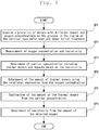
- FIG. 1 is a flowchart of steps of a preparation process in a method for measuring resistivity of Si wafers, according to the present invention
- FIG. 2 is a schematic view of a vertical furnace to be used in the method for measuring resistivity of Si wafers, according to the present invention.
- Si wafers (with a diameter of 200 mm, for example) are mounted with a substantially equal spacing on a vertical boat 1 shown in FIG. 2 that has a hundred and twenty (120) grooves for mounting, for example (Step S1 in FIG. 1 ).
- Each wafer W to be used contain the same dopant concentration and oxygen concentration.
- five or more dummy wafers DW are mounted adjacent to the upper and lower side of Si product wafers.
- the vertical boat 1 is accommodated into the vertical heat treatment furnace 2 to perform the donor killer process at 650 °C for 30 minutes in a N 2 atmosphere (Step S2 in FIG. 1 ) .
- the resistivity of each wafer W is measured after extracting the wafers W from the furnace at a speed of 100 mm/min that is a moving speed of the boat elevator. Measurement of the resistivity is carried out using a four-probe method that employs four needle electrodes (Step S3 in FIG.1 ). A region in the vertical boat 1 where the measured resistivity is found to be substantially constant is identified in a vertical position of the boat 1 (Step S4 in FIG.1 ). The identified region is called "a region of stable-resistivity grooves" in the present embodiment.
- a plurality of Si wafers W having different levels of oxygen concentration is mounted on the region of resistivity-stable grooves of the vertical boat 1 (Step S5 in FIG. 1 ), and the donor killer process is performed at a temperature of 650 °C for 30 min. in an N 2 atmosphere in the vertical heat treatment furnace 2 (Step S6 in FIG. 1 ).
- the resistivity of a first resistivity group and oxygen concentration are measured (Step S7 in FIG. 1 ).
- the measurement of the oxygen concentration is performed using an infrared absorption method, more specifically, a Fourier transform infrared spectroscopy (FT-IR) . Accordingly the resistivity of the first resistivity group is the one subjected to influences of dopants and thermal donors.
- FT-IR Fourier transform infrared spectroscopy
- a plurality of Si wafer prepared under the same condition as for steps S5 and S6 is then thermally processed in a single-wafer type rapid thermal processing (RTP) furnace at a temperature of 650 °C or higher for 30 min. in an N 2 atmosphere, and then cooled down to 300 °C at a rate of 50 °C/s or faster.
- RTP rapid thermal processing
- a donor killer process thermal donors are prevented from being regenerated and the resistivity is free from influences of the donors.
- the resistivity of a second resistivity group and oxygen concentration of the wafers are measured (Step S8 in FIG. 1 ); the resistivity is solely affected by dopants and free from influences of the thermal donors.
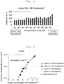
- the expression (1) which shows a relationship between the concentrations of regenerated thermal donors against the respective oxygen concentration, is obtained on the basis of the difference of the resistivity measured in the step S7 and measured in the step S8. Specifically, the concentration of thermal donors is obtained for the respective wafers W having different oxygen concentration levels from the difference of resistivity values measured in the step S7 and in the step S8, and the obtained concentrations are plotted to graph. That is, as shown in FIG. 6 , for example, an approximation curve (a general expression) is obtained wherein let the vertical axis be an logarithm of the concentration of thermal donors and the horizontal axis be the oxygen concentration, and then the obtained expression corresponds to the relational expression (1) .
- the resistivity and the concentration of thermal donors can be estimated by using Irvin's curve, which is a general relationship between resistivity and carrier concentration including dopant concentration and thermal donor concentration, when the influence of a dopant atom and a thermal donor to the resistivity is considered to be equivalent. Namely, this estimation can be carried out using the following expressions (2) and (3) that are standardized by SEMI Standards (SEMI-MF723); the expression (2) shows a relationship of acceptor concentration and resistivity and expression (3) shows a relationship of donor concentration and resistivity, where N A denotes Boron concentration and ⁇ denotes resistivity in expression (2), and N D denotes phosphor concentration and ⁇ denotes resistivity in expression (3).
- N A 1.330 ⁇ 10 16 / ⁇ + 1.082 ⁇ 10 17 / ⁇ 1 + 54.56 1.105
- N D 6.242 ⁇ 10 18 ⁇ 10 z / ⁇ ,
- FIG. 3 is a flowchart of steps of an operation procedure in the method for measuring resistivity of Si wafers, according to the present invention.
- product wafers W are subjected to the donor killer process (Step SP1 in FIG.3 ); the wafers having different dopant and oxygen concentration are mounted on the region of resistivity-stable grooves of the vertical boat1 and heated at 650 °C or higher for 30 min in an N 2 atmosphere in a vertical furnace.
- the wafers W are extracted from the furnace at a speed of 100 mm/min. Resistivity subjected to influences of thermal donors and concentration of oxygen of the wafers W are measured (Step SP2 in FIG.3 ), where thermal donors are regenerated due to a thermal history of 450 °C. Carrier concentration of the each wafer W is obtained from the measured resistivity based on Irvin's curve (Step SP3 in FIG. 3 ) ; the carrier concentration value includes that of thermal donors and the dopant.
- the concentration of the thermal donors of each wafer W is obtained from the measured oxygen concentration in the step SP2 using the relational expression (1) (Step SP4 in FIG. 3 ).
- carrier concentration solely due to the dopants is obtained by subtracting that of the thermal donors obtained in the step SP4 from the carrier concentration obtained in the step SP3 (Step SP5 in FIG. 3 ).
- the resistivity solely due to the dopant is available by correcting on the basis of the relational expression (1) obtained beforehand to eliminate the influence of the thermal donors that are regenerated during extraction from the furnace due to a thermal history of 450 °C, when wafers are subjected to the donor-killer process collectively in the vertical furnace.
- the resistivity solely due to the dopant is accurately evaluated after the wafers have been heat-treated in a vertical furnace which ensures high productivity, that is high working efficiency.
- the measurement method according to the present invention is not restricted by the characteristics of wafers whose resistivity is to be measured.
- the present invention is more effective because the influence of thermal donors to resistivity variation becomes more significant for high resistivity, which is 2 ⁇ -m or higher, for example.
- n-type Si wafers with a diameter of 200 mm, having oxygen concentration of 1.0x10 18 atoms/cm 3 (Old ASTM), were prepared and mounted on a vertical boat along the vertical direction at equal intervals.
- the boat was accommodated in a vertical furnace and a donor killer process was performed at a maximum temperature of 650 °C for 30 min in an N 2 atmosphere.
- wafers are extracted at a speed of 100 mm/min and the resistivity of the wafers were measured.
- FIG.4 A graph of resistivity of wafers after heat treatment mounted from the upper to lower regions of the boat is shown in FIG.4 , where the vertical axis is resistivity ( ⁇ -m) and the horizontal axis is position of grooves on the boat.
- FIG. 4 shows that the resistivity at the lower region of the boat is lower, and higher at the upper region of the boat, and substantially constant at the central region. It is confirmed from the above results that the experiencing time of 450 °C may presumably have an influence to resistivity of wafers, and that the central region of the boat may be defined as a resistivity-stable region.
- steps of obtaining a relational expression that relates oxygen concentration to a concentration of thermal donors were performed in EXPERIMENT 2.
- a plurality of n-type Si wafers W having different oxygen concentration levels were mounted on grooves in the resistivity-stable region of the vertical boat.
- the vertical boat was accommodated in the vertical furnace.
- the donor killer process was performed at a maximum temperature of 650 °C for 30 min in an N 2 atmosphere.
- Oxygen concentration and resistivity of the first resistivity group of the wafers were measured; the oxygen concentration and the dopant concentration converted from the resistivity are shown in a column of the vertical furnace of a table in FIG. 7 .
- a plurality of Si wafers W were subjected to a heat treatment at a maximum temperature of 650 °C for 30 min in an N 2 atmosphere in a single-wafer type RTP furnace, and cooled down to 300 °C at a cooling speed of faster than 50 °C/s. Then, oxygen concentration and resistivity of the second resistivity group of the wafers were measured; the oxygen concentration and the dopant concentration converted from the resistivity are shown in a column of RTP of the table in FIG 7 .
- a relation between the oxygen concentration and the concentration of thermal donors for each oxygen concentration level was obtained from the difference of resistivity of the first and second resistivity group corresponding to the difference of the concentration of dopant, i.e., the estimated values in the table of FIG. 7 .
- the results are plotted on a graph in FIG. 5 , where the horizontal axis denotes the oxygen concentration (/cm 3 ) and the vertical axis the concentration of thermal donors (10 18 atoms/cm 3 ).
- p-type and n-type Si wafers were mixedly mounted on grooves in the resistivity-stable region of a first vertical boat in the vertical furnace, and were subjected to a heat treatment at 650 °C or higher for 30 min, and cooled down to 300 °C and extracted at an elevator moving speed, or extraction speed, of 100 mm/min. After extraction, the concentration of thermal donors against the oxygen concentration of each wafer are plotted on a graph shown in FIG. 5 , where a cross ⁇ and a triangle ⁇ denote values for p-type and n-type wafers, respectively.
Landscapes
- Engineering & Computer Science (AREA)
- Manufacturing & Machinery (AREA)
- Power Engineering (AREA)
- Microelectronics & Electronic Packaging (AREA)
- Computer Hardware Design (AREA)
- Chemical & Material Sciences (AREA)
- General Physics & Mathematics (AREA)
- Physics & Mathematics (AREA)
- Health & Medical Sciences (AREA)
- General Health & Medical Sciences (AREA)
- Immunology (AREA)
- Pathology (AREA)
- Biochemistry (AREA)
- Analytical Chemistry (AREA)
- Life Sciences & Earth Sciences (AREA)
- Electrochemistry (AREA)
- Chemical Kinetics & Catalysis (AREA)
- Testing Or Measuring Of Semiconductors Or The Like (AREA)
- Crystals, And After-Treatments Of Crystals (AREA)
Abstract
Description
- This invention relates to methods for measuring resistivity of Si wafers, specifically relates to a method for measuring resistivity of silicon wafers that enables to accurately measure the resistivity of Si wafers having high resistivity and a large diameter.
- As for resistivity of Si wafers, the resistivity solely due to the remained dopant is obtained, after thermal donors that are generated through a thermal history at 450°C during crystal growth have been annihilated by a heat treatment at 650°C or more (Hereinafter as a donor killer heat treatment) . As is commonly known, the resistivity, however, of wafers having a high resistivity of 2 Ω-m or more largely varies due to thermal donors generated in the thermal history passing through 450 °C when the temperature of the furnace is lowered from a donor killer treatment temperature to room temperature.
- A patent literature
JP No. 2003-240689 A - Large diameter wafers, such as 8 inches or larger, wafers may have a risk of breakage due to thermal stress during heat treatment or cooling because of the large size when processed in a horizontal furnace. For this reason, a plurality of large diameter wafers is commonly heat-treated in a vertical type furnace. The wafers cannot be cooled rapidly because the vertical type furnace for donor killer processing requires elevation/lowering by a boat elevator when the wafers are extracted. This causes regeneration of thermal donors due to a thermal history at 450 °C at extraction from the furnace.
- For this problem, Japanese Patent No.
4970724 - Silicon crystals, however, being doped with carbon may possibly be shipped if a method with doped carbon as disclosed in PL2 is employed to prevent the generation of thermal donors; when a heat treatment is performed at customers' site, the carbon in Si crystal may become an oxygen precipitation nucleus and cause to shorten the lifetime of devices made therefrom.
- The present invention is made under such a circumstance; it is an object to provide a method for measuring resistivity of Si wafers capable of measuring the resistivity solely due to a dopant accurately without lowering working efficiency, where, even for large wafers, wafers can be processed to control generation of thermal donors without breakage.
- The method for measuring resistivity of a Si wafer according to the present invention to solve the above problem is a method for measuring resistivity of a Si wafer having a predetermined resistivity and oxygen concentration, the method includes steps of:
- obtaining a relational expression between an oxygen concentration and a concentration of thermal donors both of which the Si wafer contains;
- measuring the resistivity and the oxygen concentration of the product wafer that is accommodated in a vertical boat, after the wafer is subjected to a donor killer treatment for annihilation of thermal donors in a vertical heat treatment furnace and the vertical boat is extracted from the vertical heat treatment furnace at a predetermined speed;
- obtaining a carrier concentration including a dopant and thermal donors based on the measured resistivity of the Si wafer;
- obtaining the concentration of the thermal donors contained in the wafer using the expression based on the measured oxygen concentration;
- obtaining a concentration of the dopant that is given by subtraction of the concentration of the thermal donors from the measured carrier concentration; and
- converting the concentration of the dopant into the resistivity.
- Further, the step of obtaining the relational expression between the concentration of the thermal donors and the oxygen concentration contained in the wafer preferably includes the following steps of:
- measuring resistivity of a first resistivity group of a plurality of Si wafers that are affected by thermal donors, the wafers including different oxygen concentration levels being mounted on the vertical boat, the wafers subjected to the donor killer treatment, and the boat being extracted at the predetermined speed from the vertical heat treatment furnace;
- measuring resistivity of a second resistivity group of a plurality of Si wafers prepared under the similar condition to include the different oxygen concentration levels, the wafers being not affected by thermal donors by being heat-treated at the same highest temperature and duration as the temperature of the donor killer treatment, cooled rapidly and extracted from the furnace;
- obtaining the relational expression of the concentration of the regenerated thermal donors for each oxygen concentration level based on difference between the resistivity of the first resistivity group and the resistivity of the second resistivity group for each oxygen concentration level.
- In addition, the wafers to be mounted on the vertical boat are preferably mounted in such a range of mounting area along the vertical direction of the vertical boat that the wafers have the same resistivity after the donor killer treatment and extraction from the furnace.
- Further, the highest temperature of the donor killer treatment is preferably at least 650 °C and duration is preferably at least 30 min.
- The extraction speed of the vertical boat from the vertical heat treatment furnace is preferably at least 100 mm/min.
- The relational expression can be given by an expression (1) below, by letting TD denote the concentration of the thermal donors, Oi the oxygen concentration, A a coefficient, and B an exponent:

- According to the method above for measuring resistivity, when the killer treatment is carried out collectively in a vertical-type heat treatment furnace (hereinafter referred to as a vertical furnace), the resistivity solely due to the dopant can be obtained based on the relational expression obtained beforehand, by eliminating an influence due to the thermal donors that are regenerated by experiencing the thermal history of 450 °C during extraction from the furnace.
- Thus even for large diameter Si wafers, the resistivity solely due to the dopant is accurately evaluated after the wafers have been heat-treated in a vertical furnace which ensures high productivity, that is high working efficiency.
-
-
FIG. 1 is a flowchart of steps of a preparation process in a method for measuring resistivity of Si wafers, according to the present invention; -
FIG. 2 is a schematic view of a vertical furnace to be used in the method for measuring resistivity of Si wafers, according to the present invention; -
FIG. 3 is a flowchart of steps of an operation procedure in the method for measuring resistivity of Si wafers, according to the present invention; -
FIG. 4 is a graph showing a result of an embodiment of the method for measuring resistivity of Si wafers, according to the present invention; -
FIG. 5 is a graph showing a result of another embodiment of the method for measuring resistivity of Si wafers, according to the present invention; -
FIG. 6 is a graph showing a relational expression (a general formula) between a concentration of regenerated thermal donors and each oxygen concentration contained in a Si wafer in the method for measuring resistivity of Si wafers according to the present invention; and -
FIG. 7 is a table showing results of embodiments of the method for measuring resistivity of Si wafers according to the present invention. - A method for measuring resistivity of Si wafers according to the present invention will be explained with reference to the drawings.
- For the method according to the present invention, a vertical furnace is employed that is not a single-wafer type apparatus but can accommodate a plurality of Si wafers and perform thermal processing collectively. The method further performs a donor killer treatment where wafers are heated to a predetermined temperature to annihilate thermal donors and obtain the resistivity solely due to dopants in consideration of regenerated thermal donors.
- In the present invention, preparatory processes before operation steps are carried out beforehand in order to obtain a relational expression to give a concentration of regenerated thermal donors of each of the wafers.
-
FIG. 1 is a flowchart of steps of a preparation process in a method for measuring resistivity of Si wafers, according to the present invention, andFIG. 2 is a schematic view of a vertical furnace to be used in the method for measuring resistivity of Si wafers, according to the present invention. - Firstly, twenty (20) Si wafers (with a diameter of 200 mm, for example) are mounted with a substantially equal spacing on a
vertical boat 1 shown inFIG. 2 that has a hundred and twenty (120) grooves for mounting, for example (Step S1 inFIG. 1 ). Each wafer W to be used contain the same dopant concentration and oxygen concentration. In the vertical boat, five or more dummy wafers DW are mounted adjacent to the upper and lower side of Si product wafers. - Then, as shown in
FIG. 1 , thevertical boat 1 is accommodated into the verticalheat treatment furnace 2 to perform the donor killer process at 650 °C for 30 minutes in a N2 atmosphere (Step S2 inFIG. 1 ) . - Subsequently, the resistivity of each wafer W is measured after extracting the wafers W from the furnace at a speed of 100 mm/min that is a moving speed of the boat elevator. Measurement of the resistivity is carried out using a four-probe method that employs four needle electrodes (Step S3 in
FIG.1 ). A region in thevertical boat 1 where the measured resistivity is found to be substantially constant is identified in a vertical position of the boat 1 (Step S4 inFIG.1 ). The identified region is called "a region of stable-resistivity grooves" in the present embodiment. - Next, a plurality of Si wafers W having different levels of oxygen concentration is mounted on the region of resistivity-stable grooves of the vertical boat 1 (Step S5 in
FIG. 1 ), and the donor killer process is performed at a temperature of 650 °C for 30 min. in an N2 atmosphere in the vertical heat treatment furnace 2 (Step S6 inFIG. 1 ). After extraction from the furnace at a speed of 100 mm/min, the resistivity of a first resistivity group and oxygen concentration are measured (Step S7 inFIG. 1 ). The measurement of the oxygen concentration is performed using an infrared absorption method, more specifically, a Fourier transform infrared spectroscopy (FT-IR) . Accordingly the resistivity of the first resistivity group is the one subjected to influences of dopants and thermal donors. - A plurality of Si wafer prepared under the same condition as for steps S5 and S6 is then thermally processed in a single-wafer type rapid thermal processing (RTP) furnace at a temperature of 650 °C or higher for 30 min. in an N2 atmosphere, and then cooled down to 300 °C at a rate of 50 °C/s or faster. In the wafers thus processed, a donor killer process, thermal donors are prevented from being regenerated and the resistivity is free from influences of the donors. The resistivity of a second resistivity group and oxygen concentration of the wafers are measured (Step S8 in
FIG. 1 ); the resistivity is solely affected by dopants and free from influences of the thermal donors. - The expression (1), which shows a relationship between the concentrations of regenerated thermal donors against the respective oxygen concentration, is obtained on the basis of the difference of the resistivity measured in the step S7 and measured in the step S8. Specifically, the concentration of thermal donors is obtained for the respective wafers W having different oxygen concentration levels from the difference of resistivity values measured in the step S7 and in the step S8, and the obtained concentrations are plotted to graph. That is, as shown in
FIG. 6 , for example, an approximation curve (a general expression) is obtained wherein let the vertical axis be an logarithm of the concentration of thermal donors and the horizontal axis be the oxygen concentration, and then the obtained expression corresponds to the relational expression (1) . - The relational expression can be given by an expression (1) below, by letting TD denote the concentration of the thermal donors, Oi the oxygen concentration, A a coefficient, and B an exponent:

- The resistivity and the concentration of thermal donors can be estimated by using Irvin's curve, which is a general relationship between resistivity and carrier concentration including dopant concentration and thermal donor concentration, when the influence of a dopant atom and a thermal donor to the resistivity is considered to be equivalent. Namely, this estimation can be carried out using the following expressions (2) and (3) that are standardized by SEMI Standards (SEMI-MF723); the expression (2) shows a relationship of acceptor concentration and resistivity and expression (3) shows a relationship of donor concentration and resistivity, where NA denotes Boron concentration and ρ denotes resistivity in expression (2), and ND denotes phosphor concentration and ρ denotes resistivity in expression (3).


- where z = (A0+A1X+A2X2+A3X3)/(1+B1X+B2X2+B3X3),
- X = log10 ρ, and
- A0 = -3.1083, A1 = -3.2626, A2 = -1.2196, A3 = -0.13923,
- B1 = 1.0265, B2 = 0.38755, B3 = 0.041833.
- After the expression (1) for obtaining the concentration of regenerated thermal donors is thus obtained, an operation procedure for determining resistivity solely due to dopants can be carried out.
-
FIG. 3 is a flowchart of steps of an operation procedure in the method for measuring resistivity of Si wafers, according to the present invention. - In the operation procedure, product wafers W are subjected to the donor killer process (Step SP1 in
FIG.3 ); the wafers having different dopant and oxygen concentration are mounted on the region of resistivity-stable grooves of the vertical boat1 and heated at 650 °C or higher for 30 min in an N2 atmosphere in a vertical furnace. - The wafers W are extracted from the furnace at a speed of 100 mm/min. Resistivity subjected to influences of thermal donors and concentration of oxygen of the wafers W are measured (Step SP2 in
FIG.3 ), where thermal donors are regenerated due to a thermal history of 450 °C. Carrier concentration of the each wafer W is obtained from the measured resistivity based on Irvin's curve (Step SP3 inFIG. 3 ) ; the carrier concentration value includes that of thermal donors and the dopant. - The concentration of the thermal donors of each wafer W is obtained from the measured oxygen concentration in the step SP2 using the relational expression (1) (Step SP4 in
FIG. 3 ). - Then carrier concentration solely due to the dopants is obtained by subtracting that of the thermal donors obtained in the step SP4 from the carrier concentration obtained in the step SP3 (Step SP5 in
FIG. 3 ). - It should be noted that the unit of the carrier concentration and the concentration of donors is cm-3 and the concentration of the dopants is atoms/cm3. Since a single dopant atom releases a single carrier, the carrier concentration equals to the dopant concentration, if there are no thermal donors.
Therefore, the carrier concentration for n-type semiconductor is given by
carrier concentration = dopant concentration + concentration of thermal donors,
and that for p-type semiconductor is given by
FIG.3 ). - As in the embodiment described above according to the present invention, the resistivity solely due to the dopant is available by correcting on the basis of the relational expression (1) obtained beforehand to eliminate the influence of the thermal donors that are regenerated during extraction from the furnace due to a thermal history of 450 °C, when wafers are subjected to the donor-killer process collectively in the vertical furnace.
- Thus even for large diameter Si wafers, the resistivity solely due to the dopant is accurately evaluated after the wafers have been heat-treated in a vertical furnace which ensures high productivity, that is high working efficiency.
- The measurement method according to the present invention is not restricted by the characteristics of wafers whose resistivity is to be measured. The present invention, however, is more effective because the influence of thermal donors to resistivity variation becomes more significant for high resistivity, which is 2 Ω-m or higher, for example.
- The measurement method according to the present invention for resistivity of Si wafers will be further explained based on embodiments. In the embodiments the following experiments were performed.
- In
Experiment 1, among the steps the preparation process shown inFIG. 1 , steps up to obtainment of a region of resistivity-stable grooves are performed. - Twenty (20) n-type Si wafers with a diameter of 200 mm, having oxygen concentration of 1.0x10¹⁸ atoms/cm3 (Old ASTM), were prepared and mounted on a vertical boat along the vertical direction at equal intervals. The boat was accommodated in a vertical furnace and a donor killer process was performed at a maximum temperature of 650 °C for 30 min in an N2 atmosphere. After the treatment, wafers are extracted at a speed of 100 mm/min and the resistivity of the wafers were measured. In addition temperature change at positions of the vertical boat, the upper, central and the lower region, was observed during the process from the heat treatment to extraction. This experiment gave results that the experiencing time, or passing duration, at a temperature of 450 °C at which thermal donors are to be regenerated is the longest at the lower region of the boat and the shortest at the upper region, and that there exists a region where the experiencing time of 450 °C is constant in the central region.
- A graph of resistivity of wafers after heat treatment mounted from the upper to lower regions of the boat is shown in
FIG.4 , where the vertical axis is resistivity (Ω-m) and the horizontal axis is position of grooves on the boat. AsFIG. 4 shows that the resistivity at the lower region of the boat is lower, and higher at the upper region of the boat, and substantially constant at the central region.
It is confirmed from the above results that the experiencing time of 450 °C may presumably have an influence to resistivity of wafers, and that the central region of the boat may be defined as a resistivity-stable region. - Among the steps of a preparation process shown in
FIG. 1 , steps of obtaining a relational expression that relates oxygen concentration to a concentration of thermal donors were performed inEXPERIMENT 2. A plurality of n-type Si wafers W having different oxygen concentration levels were mounted on grooves in the resistivity-stable region of the vertical boat. The vertical boat was accommodated in the vertical furnace. The donor killer process was performed at a maximum temperature of 650 °C for 30 min in an N2 atmosphere. Oxygen concentration and resistivity of the first resistivity group of the wafers were measured; the oxygen concentration and the dopant concentration converted from the resistivity are shown in a column of the vertical furnace of a table inFIG. 7 . - In addition, a plurality of Si wafers W were subjected to a heat treatment at a maximum temperature of 650 °C for 30 min in an N2 atmosphere in a single-wafer type RTP furnace, and cooled down to 300 °C at a cooling speed of faster than 50 °C/s. Then, oxygen concentration and resistivity of the second resistivity group of the wafers were measured; the oxygen concentration and the dopant concentration converted from the resistivity are shown in a column of RTP of the table in
FIG 7 . - A relation between the oxygen concentration and the concentration of thermal donors for each oxygen concentration level was obtained from the difference of resistivity of the first and second resistivity group corresponding to the difference of the concentration of dopant, i.e., the estimated values in the table of
FIG. 7 . The results are plotted on a graph inFIG. 5 , where the horizontal axis denotes the oxygen concentration (/cm3) and the vertical axis the concentration of thermal donors (1018 atoms/cm3). A relational expression (4) is obtained from the curve plotted in the graph,
- In
EXPERIMENT 3, p-type and n-type Si wafers were mixedly mounted on grooves in the resistivity-stable region of a first vertical boat in the vertical furnace, and were subjected to a heat treatment at 650 °C or higher for 30 min, and cooled down to 300 °C and extracted at an elevator moving speed, or extraction speed, of 100 mm/min. After extraction, the concentration of thermal donors against the oxygen concentration of each wafer are plotted on a graph shown inFIG. 5 , where a cross × and a triangle Δ denote values for p-type and n-type wafers, respectively. - Then, p-type and n-type Si wafers were mixedly mounted on grooves in the resistivity-stable region of a second vertical boat in the vertical furnace, and were subjected to a heat treatment at 650 °C or higher for 30 min, and cooled down to 300 °C and extracted at an elevator moving speed, or extraction speed, of 100 mm/min. After extraction, the concentration of thermal donors against the oxygen concentration of each wafer are plotted on a graph shown in
FIG. 5 , where a rhombus ◊ and a square □ denote values for p-type and n-type wafers, respectively. All the values of the results of the experiments above are plotted along a curve given by the expression (4). Therefore, it is confirmed that the expression (2) obtained inEPERIMENT 2 can be applicable to cases of heat treatment under the same condition, regardless of p-type or n-type Si wafers. -
- 1
- a vertical boat
- 2
- a vertical-type heat treatment furnace
- W
- Si wafer(s)
Claims (6)
- A method for measuring resistivity of a Si wafer having a predetermined resistivity and oxygen concentration, the method comprising:a step of obtaining a relational expression between oxygen concentration and concentration of thermal donors;a step of measuring the resistivity and the oxygen concentration of a product wafer accommodated in a vertical boat, after the wafer being subjected to a donor killer treatment for annihilation of thermal donors in a vertical heat treatment furnace, and the vertical boat being extracted from the vertical heat treatment furnace at a predetermined speed;a step of obtaining concentration of carriers including a dopant and thermal donors based on the measured resistivity of the Si wafer;a step of obtaining the concentration of the thermal donors contained in the wafer using the expression based on the measured oxygen concentration;a step of obtaining the concentration of the dopant that is found by subtracting the concentration of the thermal donors from the measured carrier concentration; anda step of converting the concentration of the dopant into resistivity.
- The method for measuring the resistivity according to Claim 1, wherein the step of obtaining the relational expression between the concentration of the thermal donors and the oxygen concentration contained in the wafer further comprises
a step of measuring resistivity of a first resistivity group of a plurality of Si wafers that are affected by thermal donors, wherein each of the wafers includes different oxygen concentration levels, the wafers accommodated in the vertical boat are subjected to a donor killer treatment, and the boat is extracted at a predetermined speed from the vertical heat treatment furnace;
a step of measuring resistivity of a second resistivity group of a plurality of Si wafers that are prepared under a similar condition in which each of the plurality of Si wafers includes the different oxygen concentration levels, wherein the wafers are subjected to a heat treatment at a temperature and a time duration same as those in the donor killer treatment, and the boat is extracted at a predetermined speed from the vertical heat treatment furnace; and
a step of obtaining the relational expression of concentration of regenerated thermal donors for each oxygen concentration level based on differences between the resistivity of the first resistivity group and the resistivity of the second resistivity group for each oxygen concentration level. - The method for measuring the resistivity according to Claim 1, wherein the wafers to be accommodated in the vertical boat are mounted in a range of mounting area along a vertical direction of the vertical boat such that the wafers have the same resistivity after subjected to the donor killer treatment and extracted from the vertical heat treatment furnace.
- The method for measuring the resistivity according to Claim 1, wherein a maximum temperature of the donor killer treatment is at least 650 °C and time duration is at least 30 min.
- The method for measuring the resistivity according to Claim 1, wherein an extraction speed of the vertical boat from the vertical heat treatment furnace is preferably at least 100 mm/min.
- The method for measuring the resistivity according to Claim 1, wherein the relational expression is given by an expression (1) below, by letting TD denote the concentration of the thermal donors, Oi the oxygen concentration, A a coefficient, and B an exponent:

Applications Claiming Priority (1)
| Application Number | Priority Date | Filing Date | Title |
|---|---|---|---|
| JP2017144060A JP6878188B2 (en) | 2017-07-26 | 2017-07-26 | How to measure the resistivity of a silicon wafer |
Publications (1)
| Publication Number | Publication Date |
|---|---|
| EP3435409A1 true EP3435409A1 (en) | 2019-01-30 |
Family
ID=62750760
Family Applications (1)
| Application Number | Title | Priority Date | Filing Date |
|---|---|---|---|
| EP18177257.5A Pending EP3435409A1 (en) | 2017-07-26 | 2018-06-12 | Method for measuring resistivity of silicon wafers |
Country Status (5)
| Country | Link |
|---|---|
| EP (1) | EP3435409A1 (en) |
| JP (1) | JP6878188B2 (en) |
| KR (1) | KR102137867B1 (en) |
| CN (1) | CN109307804B (en) |
| TW (1) | TWI712792B (en) |
Families Citing this family (2)
| Publication number | Priority date | Publication date | Assignee | Title |
|---|---|---|---|---|
| CN113109625A (en) * | 2021-04-07 | 2021-07-13 | 上海新昇半导体科技有限公司 | Method for judging conductive type of silicon wafer |
| CN113721076A (en) * | 2021-08-09 | 2021-11-30 | 上海新昇半导体科技有限公司 | Method for measuring resistivity of silicon wafer |
Citations (5)
| Publication number | Priority date | Publication date | Assignee | Title |
|---|---|---|---|---|
| JPH04259214A (en) * | 1991-02-13 | 1992-09-14 | Mitsubishi Materials Corp | Measuring method of temperature distribution in heat treating furnace |
| JPH0982768A (en) * | 1995-09-19 | 1997-03-28 | Hitachi Ltd | Evaluating method for semiconductor wafer |
| JP2003240689A (en) | 2002-02-13 | 2003-08-27 | Shin Etsu Handotai Co Ltd | Automatic processing method and system of sample for inspecting semiconductor crystal, and method of inspecting semiconductor crystal |
| JP4970724B2 (en) | 2002-07-17 | 2012-07-11 | 株式会社Sumco | Manufacturing method of high resistance silicon wafer |
| US20140033797A1 (en) * | 2011-04-15 | 2014-02-06 | Commissariat A L'energie Atomique Et Aux Energies Alternatives | Method for determining interstitial oxygen concentration |
Family Cites Families (12)
| Publication number | Priority date | Publication date | Assignee | Title |
|---|---|---|---|---|
| JPH0750713B2 (en) * | 1990-09-21 | 1995-05-31 | コマツ電子金属株式会社 | Heat treatment method for semiconductor wafers |
| JP2869300B2 (en) * | 1992-08-07 | 1999-03-10 | 三菱マテリアル株式会社 | Semiconductor wafer heat treatment equipment |
| CN100389489C (en) * | 2003-12-30 | 2008-05-21 | 中芯国际集成电路制造(上海)有限公司 | Low energy dosage monitoring using wafer impregnating machine |
| CN101527273B (en) * | 2009-04-10 | 2012-04-18 | 中国科学院光电技术研究所 | Measuring device for semiconductor material characteristics |
| JP5678846B2 (en) * | 2011-09-08 | 2015-03-04 | 信越半導体株式会社 | Method for calculating nitrogen concentration in silicon single crystal and calculating resistance shift amount |
| CN102688859B (en) * | 2012-06-13 | 2013-08-07 | 东莞市科隆威自动化设备有限公司 | Plate dividing machine for photovoltaic detection |
| JP6045842B2 (en) * | 2012-07-31 | 2016-12-14 | 株式会社国際電気セミコンダクターサービス | Resistivity measuring apparatus and method |
| FR2997096B1 (en) * | 2012-10-23 | 2014-11-28 | Commissariat Energie Atomique | PROCESS FOR FORMING A SILICON INGOT OF UNIFORM RESISTIVITY |
| CN102928669A (en) * | 2012-10-25 | 2013-02-13 | 上海宏力半导体制造有限公司 | Resistivity test method and resistivity test structure for semiconductor silicon wafer |
| CN104280616B (en) * | 2013-07-12 | 2017-03-22 | 苏州博昇科技有限公司 | Silicon wafer resistivity measurement device and method |
| FR3009380B1 (en) * | 2013-08-02 | 2015-07-31 | Commissariat Energie Atomique | PROCESS FOR LOCATING A PLATELET IN ITS INGOT |
| US9768056B2 (en) * | 2013-10-31 | 2017-09-19 | Sunedison Semiconductor Limited (Uen201334164H) | Method of manufacturing high resistivity SOI wafers with charge trapping layers based on terminated Si deposition |
-
2017
- 2017-07-26 JP JP2017144060A patent/JP6878188B2/en active Active
-
2018
- 2018-06-08 TW TW107119841A patent/TWI712792B/en active
- 2018-06-12 EP EP18177257.5A patent/EP3435409A1/en active Pending
- 2018-06-22 KR KR1020180071973A patent/KR102137867B1/en active IP Right Grant
- 2018-07-26 CN CN201810833673.3A patent/CN109307804B/en active Active
Patent Citations (5)
| Publication number | Priority date | Publication date | Assignee | Title |
|---|---|---|---|---|
| JPH04259214A (en) * | 1991-02-13 | 1992-09-14 | Mitsubishi Materials Corp | Measuring method of temperature distribution in heat treating furnace |
| JPH0982768A (en) * | 1995-09-19 | 1997-03-28 | Hitachi Ltd | Evaluating method for semiconductor wafer |
| JP2003240689A (en) | 2002-02-13 | 2003-08-27 | Shin Etsu Handotai Co Ltd | Automatic processing method and system of sample for inspecting semiconductor crystal, and method of inspecting semiconductor crystal |
| JP4970724B2 (en) | 2002-07-17 | 2012-07-11 | 株式会社Sumco | Manufacturing method of high resistance silicon wafer |
| US20140033797A1 (en) * | 2011-04-15 | 2014-02-06 | Commissariat A L'energie Atomique Et Aux Energies Alternatives | Method for determining interstitial oxygen concentration |
Non-Patent Citations (5)
| Title |
|---|
| BROISCH JULIANE ET AL: "A New Method for the Determination of the Dopant-Related Base Resistivity Despite the Presence of Thermal Donors", IEEE JOURNAL OF PHOTOVOLTAICS, I E E E, US, vol. 5, no. 1, 1 January 2015 (2015-01-01), pages 269 - 275, XP011568518, ISSN: 2156-3381, [retrieved on 20141218], DOI: 10.1109/JPHOTOV.2014.2360339 * |
| JORDI VEIRMAN ET AL: "A Fast and Easily Implemented Method for Interstitial Oxygen Concentration Mapping Through the Activation of Thermal Donors in Silicon", ENERGY PROCEDIA, vol. 8, 20 April 2011 (2011-04-20), pages 41 - 46, XP028263041, ISSN: 1876-6102, [retrieved on 20110812], DOI: 10.1016/J.EGYPRO.2011.06.099 * |
| KAZUMI WADA: "unified model for formation kinetics of oxygen thermal donors in silicon", PHYSICAL REVIEW, B. CONDENSED MATTER, AMERICAN INSTITUTE OF PHYSICS. NEW YORK, US, vol. 30, no. 10, 15 November 1984 (1984-11-15), pages 5884 - 5895, XP002696153, ISSN: 0163-1829, DOI: 10.1103/PHYSREVB.30.5884 * |
| NIEWELT T ET AL: "Interstitial oxygen imaging from thermal donor growth-A fast photoluminescence based me", SOLAR ENERGY MATERIALS AND SOLAR CELLS, ELSEVIER SCIENCE PUBLISHERS, AMSTERDAM, NL, vol. 131, 27 May 2014 (2014-05-27), pages 117 - 123, XP029075014, ISSN: 0927-0248, DOI: 10.1016/J.SOLMAT.2014.05.011 * |
| W. WIJARANAKULA: "Formation kinetics of oxygen thermal donors in silicon", APPLIED PHYSICS LETTERS, vol. 59, no. 13, 23 September 1991 (1991-09-23), pages 1608, XP055114038, ISSN: 0003-6951, DOI: 10.1063/1.106245 * |
Also Published As
| Publication number | Publication date |
|---|---|
| KR102137867B1 (en) | 2020-07-24 |
| TWI712792B (en) | 2020-12-11 |
| JP6878188B2 (en) | 2021-05-26 |
| CN109307804B (en) | 2021-04-30 |
| CN109307804A (en) | 2019-02-05 |
| TW201910762A (en) | 2019-03-16 |
| JP2019029387A (en) | 2019-02-21 |
| KR20190012098A (en) | 2019-02-08 |
Similar Documents
| Publication | Publication Date | Title |
|---|---|---|
| US7344689B2 (en) | Silicon wafer for IGBT and method for producing same | |
| EP1780781A1 (en) | Process for producing silicon wafer and silicon wafer produced by the process | |
| US9842779B2 (en) | Method of evaluating metal contamination in semiconductor wafer and method of manufacturing semiconductor wafer | |
| US9995693B2 (en) | Quality evaluation method for silicon wafer, and silicon wafer and method of producing silicon wafer using the method | |
| JP6083412B2 (en) | Method for controlling recombination lifetime and method for manufacturing silicon substrate | |
| EP3435409A1 (en) | Method for measuring resistivity of silicon wafers | |
| KR20160097200A (en) | Defect density evaluation method for silicon single-crystal substrate | |
| EP0550750B1 (en) | Semiconductor wafer heat treatment method | |
| US9748112B2 (en) | Quality evaluation method for silicon wafer, and silicon wafer and method of producing silicon wafer using the method | |
| TWI698935B (en) | Method for predicting thermal donor generation behavior of a silicon wafer, evaluation method of a silicon wafer, and silicon wafer manufacturing method | |
| CN111480219A (en) | Method for evaluating metal contamination | |
| Al-Amin et al. | Combining low-temperature gettering with phosphorus diffusion gettering for improved multicrystalline silicon | |
| JP7103314B2 (en) | Carbon concentration evaluation method in silicon single crystal substrate | |
| JP6607525B2 (en) | Method for measuring oxygen concentration of silicon single crystal substrate and method for manufacturing silicon single crystal substrate | |
| JP4843929B2 (en) | Heat treatment method of GaAs crystal and GaAs crystal substrate | |
| JP7582070B2 (en) | Method for predicting thermal donor behavior in silicon wafer and method for manufacturing silicon wafer | |
| US11094557B2 (en) | Silicon wafer | |
| Al‐Amin et al. | Low‐Temperature Saw Damage Gettering to Improve Minority Carrier Lifetime in Multicrystalline Silicon | |
| JP6369388B2 (en) | Evaluation method of silicon single crystal substrate | |
| CN117737863A (en) | Annealing method of tellurium-doped indium antimonide wafer | |
| JP2022181130A (en) | Prediction method for thermal donor behavior of silicon wafer and manufacturing method for silicon wafer | |
| JP2016124756A (en) | Silicon wafer and method for manufacturing the same | |
| CN117219508A (en) | Method and device for processing epitaxial wafer and method for detecting epitaxial wafer | |
| CN119153347A (en) | Method for measuring temperature of semiconductor wafer | |
| CN116646244A (en) | Method and device for processing epitaxial wafer and method for detecting epitaxial wafer |
Legal Events
| Date | Code | Title | Description |
|---|---|---|---|
| PUAI | Public reference made under article 153(3) epc to a published international application that has entered the european phase |
Free format text: ORIGINAL CODE: 0009012 |
|
| STAA | Information on the status of an ep patent application or granted ep patent |
Free format text: STATUS: THE APPLICATION HAS BEEN PUBLISHED |
|
| AK | Designated contracting states |
Kind code of ref document: A1 Designated state(s): AL AT BE BG CH CY CZ DE DK EE ES FI FR GB GR HR HU IE IS IT LI LT LU LV MC MK MT NL NO PL PT RO RS SE SI SK SM TR |
|
| AX | Request for extension of the european patent |
Extension state: BA ME |
|
| STAA | Information on the status of an ep patent application or granted ep patent |
Free format text: STATUS: REQUEST FOR EXAMINATION WAS MADE |
|
| 17P | Request for examination filed |
Effective date: 20190725 |
|
| RBV | Designated contracting states (corrected) |
Designated state(s): AL AT BE BG CH CY CZ DE DK EE ES FI FR GB GR HR HU IE IS IT LI LT LU LV MC MK MT NL NO PL PT RO RS SE SI SK SM TR |
|
| STAA | Information on the status of an ep patent application or granted ep patent |
Free format text: STATUS: EXAMINATION IS IN PROGRESS |
|
| 17Q | First examination report despatched |
Effective date: 20210622 |
|
| STAA | Information on the status of an ep patent application or granted ep patent |
Free format text: STATUS: EXAMINATION IS IN PROGRESS |