EP3429087B1 - Verfahren zur synchronisierung einer aktiven belastungsmodulationsuhr in einem transponder und entsprechender transponder - Google Patents
Verfahren zur synchronisierung einer aktiven belastungsmodulationsuhr in einem transponder und entsprechender transponder Download PDFInfo
- Publication number
- EP3429087B1 EP3429087B1 EP17305918.9A EP17305918A EP3429087B1 EP 3429087 B1 EP3429087 B1 EP 3429087B1 EP 17305918 A EP17305918 A EP 17305918A EP 3429087 B1 EP3429087 B1 EP 3429087B1
- Authority
- EP
- European Patent Office
- Prior art keywords
- carrier clock
- phase
- alm
- reader
- ckalm
- Prior art date
- Legal status (The legal status is an assumption and is not a legal conclusion. Google has not performed a legal analysis and makes no representation as to the accuracy of the status listed.)
- Active
Links
- 238000000034 method Methods 0.000 title claims description 10
- 230000010363 phase shift Effects 0.000 claims description 17
- 230000005540 biological transmission Effects 0.000 claims description 16
- 238000004891 communication Methods 0.000 claims description 7
- 230000008859 change Effects 0.000 description 13
- 238000013016 damping Methods 0.000 description 8
- 230000010355 oscillation Effects 0.000 description 6
- 230000004044 response Effects 0.000 description 4
- 208000003383 pontocerebellar hypoplasia type 3 Diseases 0.000 description 3
- 230000008054 signal transmission Effects 0.000 description 3
- 239000000243 solution Substances 0.000 description 3
- BBHJTCADCKZYSO-UHFFFAOYSA-N 4-(4-ethylcyclohexyl)benzonitrile Chemical compound C1CC(CC)CCC1C1=CC=C(C#N)C=C1 BBHJTCADCKZYSO-UHFFFAOYSA-N 0.000 description 2
- 230000001939 inductive effect Effects 0.000 description 2
- 230000009467 reduction Effects 0.000 description 2
- 230000002123 temporal effect Effects 0.000 description 2
- 239000003990 capacitor Substances 0.000 description 1
- 230000001419 dependent effect Effects 0.000 description 1
- 230000000694 effects Effects 0.000 description 1
- 239000000284 extract Substances 0.000 description 1
- 238000002347 injection Methods 0.000 description 1
- 239000007924 injection Substances 0.000 description 1
- 230000007704 transition Effects 0.000 description 1
Images
Classifications
-
- H—ELECTRICITY
- H04—ELECTRIC COMMUNICATION TECHNIQUE
- H04L—TRANSMISSION OF DIGITAL INFORMATION, e.g. TELEGRAPHIC COMMUNICATION
- H04L7/00—Arrangements for synchronising receiver with transmitter
- H04L7/02—Speed or phase control by the received code signals, the signals containing no special synchronisation information
- H04L7/033—Speed or phase control by the received code signals, the signals containing no special synchronisation information using the transitions of the received signal to control the phase of the synchronising-signal-generating means, e.g. using a phase-locked loop
- H04L7/0331—Speed or phase control by the received code signals, the signals containing no special synchronisation information using the transitions of the received signal to control the phase of the synchronising-signal-generating means, e.g. using a phase-locked loop with a digital phase-locked loop [PLL] processing binary samples, e.g. add/subtract logic for correction of receiver clock
-
- H—ELECTRICITY
- H04—ELECTRIC COMMUNICATION TECHNIQUE
- H04B—TRANSMISSION
- H04B5/00—Near-field transmission systems, e.g. inductive or capacitive transmission systems
- H04B5/40—Near-field transmission systems, e.g. inductive or capacitive transmission systems characterised by components specially adapted for near-field transmission
- H04B5/45—Transponders
-
- H—ELECTRICITY
- H04—ELECTRIC COMMUNICATION TECHNIQUE
- H04B—TRANSMISSION
- H04B5/00—Near-field transmission systems, e.g. inductive or capacitive transmission systems
- H04B5/70—Near-field transmission systems, e.g. inductive or capacitive transmission systems specially adapted for specific purposes
- H04B5/77—Near-field transmission systems, e.g. inductive or capacitive transmission systems specially adapted for specific purposes for interrogation
-
- G—PHYSICS
- G06—COMPUTING; CALCULATING OR COUNTING
- G06K—GRAPHICAL DATA READING; PRESENTATION OF DATA; RECORD CARRIERS; HANDLING RECORD CARRIERS
- G06K19/00—Record carriers for use with machines and with at least a part designed to carry digital markings
- G06K19/06—Record carriers for use with machines and with at least a part designed to carry digital markings characterised by the kind of the digital marking, e.g. shape, nature, code
- G06K19/067—Record carriers with conductive marks, printed circuits or semiconductor circuit elements, e.g. credit or identity cards also with resonating or responding marks without active components
- G06K19/07—Record carriers with conductive marks, printed circuits or semiconductor circuit elements, e.g. credit or identity cards also with resonating or responding marks without active components with integrated circuit chips
- G06K19/0723—Record carriers with conductive marks, printed circuits or semiconductor circuit elements, e.g. credit or identity cards also with resonating or responding marks without active components with integrated circuit chips the record carrier comprising an arrangement for non-contact communication, e.g. wireless communication circuits on transponder cards, non-contact smart cards or RFIDs
-
- H—ELECTRICITY
- H03—ELECTRONIC CIRCUITRY
- H03C—MODULATION
- H03C3/00—Angle modulation
- H03C3/02—Details
- H03C3/09—Modifications of modulator for regulating the mean frequency
- H03C3/0908—Modifications of modulator for regulating the mean frequency using a phase locked loop
- H03C3/0916—Modifications of modulator for regulating the mean frequency using a phase locked loop with frequency divider or counter in the loop
- H03C3/0925—Modifications of modulator for regulating the mean frequency using a phase locked loop with frequency divider or counter in the loop applying frequency modulation at the divider in the feedback loop
-
- H—ELECTRICITY
- H03—ELECTRONIC CIRCUITRY
- H03C—MODULATION
- H03C3/00—Angle modulation
- H03C3/02—Details
- H03C3/09—Modifications of modulator for regulating the mean frequency
- H03C3/0908—Modifications of modulator for regulating the mean frequency using a phase locked loop
- H03C3/095—Modifications of modulator for regulating the mean frequency using a phase locked loop applying frequency modulation to the loop in front of the voltage controlled oscillator
-
- H—ELECTRICITY
- H03—ELECTRONIC CIRCUITRY
- H03L—AUTOMATIC CONTROL, STARTING, SYNCHRONISATION OR STABILISATION OF GENERATORS OF ELECTRONIC OSCILLATIONS OR PULSES
- H03L7/00—Automatic control of frequency or phase; Synchronisation
- H03L7/06—Automatic control of frequency or phase; Synchronisation using a reference signal applied to a frequency- or phase-locked loop
- H03L7/08—Details of the phase-locked loop
- H03L7/099—Details of the phase-locked loop concerning mainly the controlled oscillator of the loop
- H03L7/0991—Details of the phase-locked loop concerning mainly the controlled oscillator of the loop the oscillator being a digital oscillator, e.g. composed of a fixed oscillator followed by a variable frequency divider
-
- H—ELECTRICITY
- H03—ELECTRONIC CIRCUITRY
- H03L—AUTOMATIC CONTROL, STARTING, SYNCHRONISATION OR STABILISATION OF GENERATORS OF ELECTRONIC OSCILLATIONS OR PULSES
- H03L7/00—Automatic control of frequency or phase; Synchronisation
- H03L7/06—Automatic control of frequency or phase; Synchronisation using a reference signal applied to a frequency- or phase-locked loop
- H03L7/16—Indirect frequency synthesis, i.e. generating a desired one of a number of predetermined frequencies using a frequency- or phase-locked loop
- H03L7/18—Indirect frequency synthesis, i.e. generating a desired one of a number of predetermined frequencies using a frequency- or phase-locked loop using a frequency divider or counter in the loop
-
- H—ELECTRICITY
- H04—ELECTRIC COMMUNICATION TECHNIQUE
- H04B—TRANSMISSION
- H04B5/00—Near-field transmission systems, e.g. inductive or capacitive transmission systems
- H04B5/70—Near-field transmission systems, e.g. inductive or capacitive transmission systems specially adapted for specific purposes
- H04B5/72—Near-field transmission systems, e.g. inductive or capacitive transmission systems specially adapted for specific purposes for local intradevice communication
-
- H—ELECTRICITY
- H04—ELECTRIC COMMUNICATION TECHNIQUE
- H04J—MULTIPLEX COMMUNICATION
- H04J3/00—Time-division multiplex systems
- H04J3/02—Details
- H04J3/06—Synchronising arrangements
- H04J3/0635—Clock or time synchronisation in a network
- H04J3/0638—Clock or time synchronisation among nodes; Internode synchronisation
-
- H—ELECTRICITY
- H04—ELECTRIC COMMUNICATION TECHNIQUE
- H04L—TRANSMISSION OF DIGITAL INFORMATION, e.g. TELEGRAPHIC COMMUNICATION
- H04L27/00—Modulated-carrier systems
- H04L27/0014—Carrier regulation
-
- H—ELECTRICITY
- H04—ELECTRIC COMMUNICATION TECHNIQUE
- H04L—TRANSMISSION OF DIGITAL INFORMATION, e.g. TELEGRAPHIC COMMUNICATION
- H04L7/00—Arrangements for synchronising receiver with transmitter
- H04L7/02—Speed or phase control by the received code signals, the signals containing no special synchronisation information
- H04L7/033—Speed or phase control by the received code signals, the signals containing no special synchronisation information using the transitions of the received signal to control the phase of the synchronising-signal-generating means, e.g. using a phase-locked loop
-
- H—ELECTRICITY
- H03—ELECTRONIC CIRCUITRY
- H03L—AUTOMATIC CONTROL, STARTING, SYNCHRONISATION OR STABILISATION OF GENERATORS OF ELECTRONIC OSCILLATIONS OR PULSES
- H03L2207/00—Indexing scheme relating to automatic control of frequency or phase and to synchronisation
- H03L2207/50—All digital phase-locked loop
-
- H—ELECTRICITY
- H04—ELECTRIC COMMUNICATION TECHNIQUE
- H04L—TRANSMISSION OF DIGITAL INFORMATION, e.g. TELEGRAPHIC COMMUNICATION
- H04L27/00—Modulated-carrier systems
- H04L27/0014—Carrier regulation
- H04L2027/0024—Carrier regulation at the receiver end
-
- H—ELECTRICITY
- H04—ELECTRIC COMMUNICATION TECHNIQUE
- H04L—TRANSMISSION OF DIGITAL INFORMATION, e.g. TELEGRAPHIC COMMUNICATION
- H04L27/00—Modulated-carrier systems
- H04L27/0014—Carrier regulation
- H04L2027/0024—Carrier regulation at the receiver end
- H04L2027/0026—Correction of carrier offset
Definitions
- Embodiments of the invention relate to wireless communication between a transponder and a reader, more particularly a high frequency communication between a RFID transponder and a reader operating at 13,56 MHz, in particular RFID transponders using active load modulation (ALM) for communicating with the reader and more specifically to the synchronization between the reader carrier clock and the ALM carrier clock.
- ALM active load modulation
- a transponder may be a passive one, i.e. performing load modulation of the magnetic field generated by the reader.
- a transponder may be an active one.
- the transponder When a transponder is an active one, i.e. using active load modulation (ALM) for transmitting information to the reader, the transponder generates the magnetic field which simulates load modulation of the reading device field performed by a passive transponder.
- ALM active load modulation
- ALM needs to be used in case signal generated by passive load modulation is not strong enough to be detected by an RFID interrogator device or reader. This is the case when transponder's antenna is small or located in a challenging environment.
- All ALM systems share same requirement to actively transmit ALM carrier bursts, the frequency of the ALM carrier being identical to the carrier frequency of the reader. This means that each burst of the ALM carrier starts with the same phase difference to the carrier signal emitted by the reader. Unchanged phase also implies that the two frequencies are identical.
- Maximum phase drift of transponder reply signal comparing to reader carrier signal inside complete transponder reply frame is specified to be 30° in draft amendment to ISO/IEC 14443 standard.
- Constant phase difference between the ALM carrier and reader carrier can be achieved for example in the following way.
- a frequency source in the transponder is used to generate ALM carrier clock.
- the frequency source is occasionally corrected during the gaps in the frame when actual carrier bursts are not emitted.
- the reader carrier signal is present (on transponder antenna) so the reference frequency is available to readjust the ALM carrier frequency source.
- IFS In-Frame Synchronization
- EP 272 7255 B1 An example of a device performing an IFS is disclosed in EP 272 7255 B1 .
- phase locked loop PLL with voltage controlled oscillator (VCO), which generates clock with frequency equal to reader carrier frequency, is used to generate the ALM clock.
- VCO voltage controlled oscillator
- PLL is put in lock mode. In this lock mode, feedback is closed and PLL is locked to digitized reader carrier signal.
- transponder reply frame when ALM transmission takes place, the PLL is put in hold mode.
- VCO In hold mode PLL feedback is opened and the VCO continues to run with frequency which was previously established.
- the free-running frequency of VCO is defined by charge which is stored in loop filter. Frequency difference between ALM carrier clock generated by the VCO and reader carrier clock results in phase drift of ALM carrier clock comparing to reader carrier clock.
- This frequency difference is caused by several sources.
- First source is the difference of frequency generated by PLL system in which VCO is induced and the input carrier clock at the moment before the PLL is put on hold.
- Second source is charge injection of switch which puts PLL in hold mode (charge injected by switch changes the voltage on VCO control pin, which results in change of VCO frequency).
- the third effect is leakage on VCO control pin and loop filter (loop filter input is in high impedance state, voltage on this input is defined by stored charge, charge is modified by leakage current of electronic elements).
- phase drift generated by sources of frequency difference mentioned above has to be corrected before it drifts above the specified maximum. This is done by closing PLL feedback loop at appropriate moments inside transponder reply frame, where the ALM transmission does not take place and the clock extracted from reader carrier signal is restored on PLL input.
- ALM carrier bursts produce at the transponder antenna, signal oscillations after each ALM carrier bursts generation. And, such oscillations may disturb the synchronization between the reader carrier frequency and the ALM carrier frequency.
- the ALM carrier bursts are generated from a subcarrier modulation by a Binary Phase Shift Keying (BPSK) encoding.
- BPSK Binary Phase Shift Keying
- the synchronization is performed in the gap between two transmission bursts.
- the signal amplitude on the antenna of the transponder decays slowly without application of specific measures.
- the decay of the signal on the inductive capacity antenna last too long and does not let enough time for resynchronization.
- the solution disclosed in WO 2015/003870 A1 to shorten this decay comprises performing a controlled damping of the oscillation by specific damping means which quickly stops the oscillation built by ALM transmission.
- EP3399655 A1 according to Art. 54(3) EPC proposed to perform said in-frame synchronization of transponder when some phase change of BPSK code takes place, without performing any controlled damping through a dedicated damping system.
- EP3121755 A1 discloses a transponder synchronizing an oscillator signal to a reader signal.
- phase correction depending in particular on the used communication protocol.
- maximum phase drift of transponder reply signal comparing to reader carrier signal inside complete transponder reply frame is specified to be 30° in draft amendment to ISO/IEC 14443 standard.
- a method of wireless communication from a transponder to a reader using active load modulation comprising transmission of data frames from the transponder to the reader and synchronization between a reader carrier clock and an ALM carrier clock generated from a digital phase locked loop (DPLL) receiving said reader carrier clock.
- ALM active load modulation
- Said synchronization comprises
- DPLL only runs outside of transponder reply frame, which means that loop filter characteristic only has to be optimized for this case.
- Phase adjustment can also be done by a single pulse of restored reader carrier signal, which means that damping system can be simplified or it may in some cases not be needed at all.
- phase correction may be performed between some of the transmitted bursts, eventually between each transmitted burst, of the reply frame, or when some phase change of BPSK code takes place, for example when the phase of BPSK signal changes so that the subcarrier half-periods where there is no transmission are attached.
- said digital phase locked loop comprises a digitally controlled oscillator having an oscillator frequency equal to N times the frequency of the reader carrier clock and generating an oscillator signal to a divider performing division by N for outputting said ALM carrier clock; and correcting the phase of said ALM carrier clock comprises controlling a parameter of said divider.
- controlling a parameter of said divider comprises for example resetting the counter to a presetting value corresponding to a phase shift between the reader carrier clock and the outputted ALM carrier clock when the digital phase locked loop is in its lock mode.
- correcting the phase of said ALM carrier clock comprises for example selecting the output signal having a phase which is the closest of a desired phase corresponding to a phase shift between the reader carrier clock and the outputted ALM carrier clock when the digital phase locked loop is in its lock mode.
- the method may further comprise correcting the frequency of said digitally controlled oscillator from the phase correction of said ALM carrier clock.
- correcting the frequency of the digitally controlled oscillator may for example comprise determining the difference between the presetting value and the actual value of the counter when the counter is reset to said presetting value, determining from said difference a frequency difference, and using said frequency difference for correcting the frequency of said digitally controlled oscillator.
- a transponder configured to wireless communicate towards a reader using active load modulation, called ALM, said transponder comprising transmission means configured to transmit frames to the reader through an antenna, synchronization means comprising a digital phase locked loop adapted to receive said reader carrier clock and to generate an ALM carrier clock first correction means configured to correct the phase of said ALM carrier clock in order to keep the variation of phase difference between said ALM carrier clock and said reader carrier clock inside a target range, and control means configured outside of each transmitted frame, to place said digital phase locked loop in a lock mode in which the feedback loop is closed, and within each transmitted frame, to place said digital phase locked loop in an hold mode in which the feedback loop is opened and to activate said first correction means at least one time.
- ALM active load modulation
- control means are configured to activate said first correction means several times within each transmitted frame.
- said digital phase locked loop comprises a digitally controlled oscillator having an oscillator frequency equal to N times the frequency of the reader carrier clock and configured to generate an oscillator signal to a divider configured to perform division by N for outputting said ALM carrier clock, and said first correction means are configured to correct the phase of said ALM carrier clock by controlling a parameter of said divider.
- said divider comprises a counter configured to perform said division by N for outputting said ALM carrier clock
- said first correction means are configured to control a parameter of said divider by resetting the counter to a presetting value corresponding to a phase shift between the reader carrier clock and the outputted ALM carrier clock when the digital phase locked loop is in its lock mode.
- said divider comprises a counter configured to perform said division by N and to deliver several output signals having different phases
- said first correction means are configured to correct the phase of said ALM carrier clock by selecting the output signal having a phase which is the closest of a desired phase corresponding to a phase shift between the reader carrier clock and the outputted ALM carrier clock when the digital phase locked loop is in its lock mode.
- said digital phase locked loop includes a digitally controlled oscillator having an oscillator frequency
- said transponder further comprises second correction means configured to correct the frequency of said digitally controlled oscillator from the phase correction of said ALM carrier clock, when said digital locked loop is in its hold mode.
- said second correction means comprises determination means configured to determine the difference between the presetting value and the actual value of the counter when the counter is reset to said presetting value, and to determine from said difference a frequency difference, and said second correction means are configured to use said frequency difference for correcting the frequency of said digitally controlled oscillator.
- the transponder is configured to wireless communicate towards said reader according to a NFC protocol, for example according to ISO/IEC 14443 type B protocol.
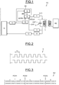
- reference TG designates a transponder or tag configured to wireless communicate towards a reader RD reading active load modulation ALM according for example to ISO/IEC 14443 type B protocol.
- the transponder TG comprises transmission means configured to transmit frames including ALM carrier bursts to the reader RD through an antenna ANT.
- Said antenna comprises an inductive element L as well as one or several capacitors C.
- the transponder comprises a demodulation circuit 10 coupled to a decoding circuit 12 for receiving data from the reader RD through antenna ANT.
- the decoding circuit 12 provides data to a processing unit 13, for example a processor, which provides also data to be sent to the reader.
- a processing unit 13 for example a processor, which provides also data to be sent to the reader.
- the data may be for example application data of a NFC (Near Field Communication) application such as transaction, payment,
- a circuit 11 extracts a clock CKR having a frequency equal to the reader carrier frequency fc, which is for example equal to 13,56 MHz in ISO/IEC 14443.
- the clock CKR is called reader carrier clock.
- the transmission means comprises encoding means 14 configured to perform here a Binary Phase Shift Keying (BPSK) data encoding.
- BPSK Binary Phase Shift Keying
- the encoding means provides to modulating means 17 (belonging to the transmission means) a data modulating signal SD using a subcarrier (here a 847,5 KHz subcarrier).
- one bit period of a bit b to be transmitted contains 8 subcarrier periods T1, which corresponds for example to ISO/IEC 14443 type B 106 kbps.
- 8 subcarrier periods are used for a bit rate of 106 kbps (fc/128).
- the number of subcarrier period is lower.
- the logical value of the bit b depends on the state high or low of the beginning of the bit period. For example, a bit period beginning with a high state and finishing with a low state may be considered as being a logical "1" whereas a bit period beginning with a low state and finishing with a high state may be considered as being a logical "0". Of course, this convention could be inverted.
- Figure 3 illustrates an example of a series of bits 1, 0, 1, 0 contained in a data signal SD.
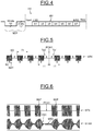
- Each byte BY of data is transmitted with a "0" start bit and a "1" stop bit as shown in figure 4 .
- the stop bit, start bit, and each data bit are one elementary time unit (ETU) in length (9.439 ⁇ S).
- ETU elementary time unit
- ISO/IEC 14443 defines a character (a byte) as comprising a start bit, eight data bits (LSB-first, MSB-last), and a stop bit.
- each frame FR comprises before the first data byte BY, a so called Start of Frame (SOF) including at least 10 bits "0" and 2 bits "1".
- SOF Start of Frame
- the modulation means 17 receive the modulating data signal SD as well as an ALM clock, called ALM carrier clock, CKALM advantageously provided by a digital phase locked loop (DPLL) 16.
- the modulation means 17 are configured to perform a subcarrier modulation with said data encoding for generating a signal STX to antenna ANT.
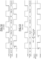
- This signal STX comprises, as illustrated in figure 5 , bursts BST of ALM carrier SC (said ALM carrier SC having a frequency equal here to 13,56 MHz).
- Two consecutive bursts BST are separated by a gap wherein no signal is transmitted from the transponder to the reader.
- Each half period of the subcarrier period T1 during which there is a signal transmission contains 8 periods of the carrier signal SC.
- the signal STX and the corresponding signal STXA at the antenna are illustrated in figure 6 .
- each generation of ALM carrier burst BST produces after said generation, signal oscillation OSC at the antenna which can decay due to specific damping means, if any, or which can naturally decrease if for example the quality factor of the antenna is moderate, for example smaller than or equal to 8 as disclosed for example in European patent application n° 17169020 mentioned above.
- the signal SRD present at the antenna corresponds to the reader carrier signal present on transponder antenna.
- Each phase change occurs when two consecutive bits having two different logical values are transmitted.
- phase change may occur during a gap where there is no signal transmission from the transponder as for example phase changes PCH1 and PCH3 or during a period where there is signal transmission as for example phase change PCH2.
- a phase change like a phase change PCH1 occurs when no burst is generated during the half period Ta2 of the subcarrier preceding the phase change PCH1 and the half period Ta1 following this phase change.
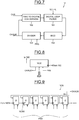
- synchronization means configured to perform synchronization between the reader carrier clock CKR and the ALM carrier clock CKALM comprises the digital phase locked loop (DPLL) 16 adapted to receive the reader carrier clock CKR and to generate the ALM carrier clock CKLM.
- DPLL digital phase locked loop
- the transponder further comprises first correction means 18 configured to deliver a correction signal, for example a presetting value PRS to the DPLL to correct the phase of the ALM carrier clock CKALM in order to keep the variation of phase difference between the ALM carrier clock CKLM and the reader carrier clock CKR inside a target range.
- a correction signal for example a presetting value PRS to the DPLL to correct the phase of the ALM carrier clock CKALM in order to keep the variation of phase difference between the ALM carrier clock CKLM and the reader carrier clock CKR inside a target range.
- the transponder further comprises control means 15 configured to deliver a control signal SCTRL to place outside of each transmitted frame FR, said digital phase locked loop 16 in a lock mode in which the feedback loop is closed and to place within each transmitted frame FR said digital phase locked loop in an hold mode in which the feedback loop is opened and to activate the first correction means at least one time within each transmitted frame.
- control means 15 configured to deliver a control signal SCTRL to place outside of each transmitted frame FR, said digital phase locked loop 16 in a lock mode in which the feedback loop is closed and to place within each transmitted frame FR said digital phase locked loop in an hold mode in which the feedback loop is opened and to activate the first correction means at least one time within each transmitted frame.
- the control means 15 may be implemented as a software module or by a logic circuit.
- the DPLL 16 When the control signal SCTRL has a first logical value, the DPLL 16 is put in a hold mode in which the feedback loop is opened, inside each transmitted frame.
- control signal STRL has a second logical value, in response of which the DPLL 16 is put in a lock mode closing the feedback loop for performing frequency synchronization between clocks CKR and CKALM.
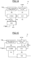
- the DPLL 16 comprises a time to digital converter based phase frequency detector 160 followed by a digital loop filter 161 followed by a digitally controlled oscillator (DCO) 162 followed by a feedback loop including a divider 163.
- the output of the divider is connected to the second entry of the time to digital converter based phase frequency detector 160.
- the first input of the time to digital converter based phase frequency detector 160 receives the clock CKR extracted from the reader carrier signal.
- the DCO is controlled by a DCO control word delivered by the digital loop filter 161.
- the DPLL When, in response to the control signal SCTRL, the DPLL is put in hold mode, the feedback loop is opened and the last DCO control word before opening the loop, is stored and used to control the DCO in the hold mode.
- DCO control is digital
- the only source of frequency difference in system using DCO is difference of frequency generated by PLL system in which DCO is induced and the input carrier signal at the moment before the PLL is put on hold.
- DCO frequency at given control word value only drifts in case supply voltage or temperature change. These changes are negligible in time period which corresponds to duration of transponder reply (few tens of ms).
- the DCO frequency does not vary inside a transponder reply frame FR.
- the DCO frequency does not change inside the transponder reply frame, it is thus not necessary to lock the DPLL 16 inside the transponder reply frame FR to correct the frequency. It is thus sufficient to only correct the phase of the ALM clock CKALM.
- DPLL only runs outside of transponder reply frame, which means that loop filter characteristic only has to be optimized for this case.
- Phase adjustment can also be done theoretically at least one time within the frame FR.
- specific damping system can be simplified or it may be in some cases not be needed at all.
- a phase adjustment may be performed between each burst BST or at each phase changes of the PCH1 or PCH3 type ( figure 3 ) or, at each phase change PCH1.
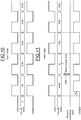
- the divider 163 is provided with a new input which is adapted to receive the presetting value PRS in order to reset the state of the divider to this presetting value.
- the phase difference between the two signals drifts in time.
- the phase is corrected by presetting the divider at least one time inside each transmitted frame FR.
- Granularity of such phase adjustment is defined by ratio between DCO frequency and reader carrier frequency. To simplify the divider this ratio is usually set to be integer. This defines granularity of phase adjustment to be 360°/n. This granularity is an additional contribution to phase variation and has to be taken in account. If for example the DCO frequency is set to 64 times transponder carrier frequency, one divider count corresponds to 360°/64 (5.625°), which is also granularity of phase adjustment system. This is variation of phase due to granularity of phase adjustment system.
- the DPLL 16 operates in the following way: DPLL only runs outside of transponder reply frame where the reader carrier clock is always present on DPLL input. Before start of transponder reply frame the DPLL feedback loop is put on hold, the value of DCO control word on output of digital loop filter is stored and used to define DCO frequency during complete transponder reply frame. Inside transponder reply frame the phase of generated ALM clock CKALM is occasionally corrected by resetting the divider with the presetting value PRS.
- the first correction means 18 are configured to control a parameter of said divider, here by resetting the counter 1630 to the presetting value PRS, in presence of a reset pulse RSP.
- the counter 1630 comprises several flip-flops, the last flip-flop delivering the clock CKALM.
- the presetting value PRS is here a digital word, stored for example in a register of said first correction means, adapted to reset the several flip-flops in order to give to the counter 1630 said presetting value.
- the presetting value corresponds to a phase shift between the reader carrier clock CKR and the outputted ALM clock CKLALM when the digital phase locked loop 16 is in its locked mode.
- figures 10 and 11 illustrate a first example of resetting the counter 1630 with a presetting value.
- Figure 10 illustrates diagrammatically the temporal evolutions of the clock CKR, the clock CKALM and the counter values of the counter 1630 when the DPLL is in its locked mode and when there is no phase shift between the signals CKR and CKALM in the locked mode.
- Figure 11 illustrates the temporal evolutions of the same signals CKR and CKALM as well as the counter values when the DPLL is in its hold mode.
- the phase difference between the two signals CKR and CKALM is equal to N periods of the digitally controlled oscillator.
- the presetting value is equal to 0 because in this embodiment, there is no phase shift between the clock CKR and the clock CKALM in the locked mode of the DPLL.
- Figures 12 and 13 illustrate the case where there is a phase shift of 10 periods of the oscillator signal delivered by the digitally controlled oscillator between the clock CKR and the clock CKALM in the lock mode of the DPLL 16.
- the counter when the DPLL is in its hold mode, the counter is reset to the presetting value equal to 64-10 in response to the reset pulse RSP in order to obtain again a phase shift of 10 periods of the oscillator signal between clock CKR and clock CKALM.
- the divider 163 comprises a Johnson counter configured to perform division by N (here division by 64) and to deliver several output signals having different phases PH0-PHn.
- the first correction means 18 are configured to correct the phase of the ALM carrier clock CKALM by selecting the output signal having a phase which is the closest of a desired phase corresponding to the phase shift between the reader carrier clock and the outputted ALM clock when the DPLL is in its lock mode.
- the first correction means will send an adjustment signal PHJ in order to select the tenth phase PH9.
- Figure 15 depicts system shown on figure 7 to which possibility to correct DCO frequency inside transmitted frame FR was added.
- Second correction means comprising determination means 1800 configured to determine the difference between the presetting value PRS and the actual value of the counter when the counter is reset to said resetting value, and to determine from said difference a frequency difference.
- Said second correction means are configured to use said frequency difference for correcting the frequency of the digitally controlled oscillator 162.
Landscapes
- Engineering & Computer Science (AREA)
- Computer Networks & Wireless Communication (AREA)
- Signal Processing (AREA)
- Computer Hardware Design (AREA)
- Microelectronics & Electronic Packaging (AREA)
- Physics & Mathematics (AREA)
- General Physics & Mathematics (AREA)
- Theoretical Computer Science (AREA)
- Stabilization Of Oscillater, Synchronisation, Frequency Synthesizers (AREA)
- Synchronisation In Digital Transmission Systems (AREA)
Claims (15)
- Verfahren zur drahtlosen Kommunikation von einem Transponder zu einem Lesegerät unter Verwendung einer aktiven Belastungsmodulation, ALM genannt, umfassend, die Übertragung von Datenrahmen von dem Transponder zu dem Lesegerät und Synchronisation zwischen einem Lesegeräteträgertakt (CKR) und einem ALM-Trägertakt (CKALM), der aus einer digitalen phasenverriegelten Schleife (16) erzeugt wird, die den Lesegeräteträgertakt (CKR) aufnimmt, wobei die Synchronisation außerhalb von jedem übertragenen Rahmen (FR) das Platzieren der digitalen phasenverriegelten Schleife (16) in einem Verriegelungsmodus umfasst, in dem die Rückmeldeschleife geschlossen ist, und innerhalb von jedem übertragenen Rahmen (FR) das Platzieren der digitalen phasenverriegelten Schleife (16) in einem Haltemodus umfasst, in dem die Rückmeldeschleife offen ist, und Korrigieren (PRS) der Phase des ALM-Trägertaktes (CKALM) mindestens einmal, um die Variation einer Phasendifferenz zwischen dem ALM-Trägertakt (CKALM) und dem Lesegeräteträgertakt (CKR) innerhalb eines Zielbereichs zu halten.
- Verfahren nach Anspruch 1, das Korrigieren (PRS) der Phase des ALM-Trägertakts (CKALM) mehrere Male innerhalb jedes übertragenen Rahmens (FR) umfassend.
- Verfahren nach Anspruch 1 oder 2, wobei die digitale phasenverriegelte Schleife (16) einen digital gesteuerten Oszillator (162) umfasst, der eine Oszillatorfrequenz gleich N mal der Frequenz des Lesegeräteträgertakts aufweist, und ein Oszillatorsignal für einen Teiler (163) erzeugt, der eine Teilung durch N zum Ausgeben des ALM-Trägertakts (CKALM) durchführt, wobei Korrigieren der Phase des ALM-Trägertakts Steuern eines Parameters des Teilers (163) umfasst.
- Verfahren nach Anspruch 3, wobei der Teiler (163) einen Zähler (1630) umfasst, der die Teilung durch N zum Ausgeben des ALM-Trägertakts (CKALM) durchführt, und wobei Steuern eines Parameters des Teilers das Zurücksetzen des Zählers auf einen Voreinstellungswert (PRS) entsprechend einem Phasenversatz zwischen dem Lesegeräteträgertakt (CKR) und dem ausgegebenen ALM-Trägertakt (CKALM) umfasst, wenn die digitale phasenverriegelte Schleife (16) in ihrem Verriegelungsmodus ist.
- Verfahren nach Anspruch 3, wobei der Teiler (163) einen Zähler umfasst, der die Teilung durch N durchführt und konfiguriert ist, um mehrere Ausgangssignale zu liefern, die unterschiedliche Phasen (PHO-PHn) aufweisen, und wobei das Korrigieren der Phase des ALM-Trägertakts (CKALM) Auswählen des Ausgangssignals umfasst, das eine Phase aufweist, die die nächstgelegene zu einer gewünschten Phase ist, die einer Phasenverschiebung zwischen dem Lesegeräteträgertakt (CKR) und dem ausgegebenen ALM-Trägertakt (CKALM) entspricht, wenn die digitale phasenverriegelte Schleife (16) in ihrem Verriegelungsmodus ist.
- Verfahren nach einem der Ansprüche 3-5, weiter umfassend, wenn die digitale phasenverriegelte Schleife, die den digital gesteuerten Oszillator beinhaltet, der eine Oszillatorfrequenz aufweist, in dem Haltemodus ist, das Korrigieren der Frequenz des digital gesteuerten Oszillators (162) aus der Phasenkorrektur des ALM-Trägertakts (CKALM).
- Verfahren nach den Ansprüchen 4 und 6, wenn von Anspruch 4 abhängig, wobei Korrigieren der Frequenz des digital gesteuerten Oszillators Bestimmen (1800) der Differenz zwischen dem Voreinstellungswert (PRS) und dem tatsächlichen Wert des Zählers umfasst, wenn der Zähler auf den Voreinstellungswert zurückgesetzt wird, Bestimmen (1800), aus der Differenz, einer Frequenzdifferenz und Verwenden der Frequenzdifferenz zum Korrigieren (1801) der Frequenz des digital gesteuerten Oszillators.
- Transponder, konfiguriert zum drahtlosen Kommunizieren zu einem Lesegerät unter Verwendung einer aktiven Belastungsmodulation, ALM genannt, umfassend Übertragungsmittel (14, 17), konfiguriert zum Übertragen von Rahmen zum Lesegerät durch eine Antenne, Synchronisationsmittel (16), umfassend eine digitale phasenverriegelte Schleife, die angepasst ist, um einen Lesegeräteträgertakt (CKR) zu empfangen und einen ALM-Trägertakt (CKALM) zu erzeugen,
erste Korrekturmittel (18), konfiguriert zum Korrigieren der Phase des ALM-Trägertakts (CKALM), um die Variation der Phasendifferenz zwischen dem ALM-Trägertakt (CKALM) und dem Lesegeräteträgertakt (CKR) innerhalb eines Zielbereichs zu halten, und
Steuerungsmittel (15), konfiguriert zum Platzieren außerhalb eines jeden übertragenen Rahmens der digitalen phasenverriegelten Schleife in einen Verriegelungsmodus, in dem die Rückmeldeschleife geschlossen ist, und zum Platzieren, innerhalb von jedem übertragenen Rahmen der digitalen phasenverriegelten Schleife in einen Haltemodus, in dem die Rückmeldeschleife offen ist, und zum Aktivieren der ersten Korrekturmittel (18) mindestens einmal innerhalb jedes übertragenen Rahmens. - Transponder nach Anspruch 8, wobei die Steuerungsmittel (15) konfiguriert sind, um die ersten Korrekturmittel (18) mehrmals innerhalb jedes übertragenen Rahmens zu aktivieren.
- Transponder nach Anspruch 8 oder 9, wobei die digitale phasenverriegelte Schleife (16) einen digital gesteuerten Oszillator (162) umfasst, der eine Oszillatorfrequenz gleich N mal der Frequenz des Lesegeräteträgertakts aufweist, um ein Oszillatorsignal für einen Teiler (163) zu erzeugen, konfiguriert, um eine Teilung durch N zum Ausgeben des ALM-Trägertakts (CKALM) durchzuführen, und die ersten Korrekturmittel (18) konfiguriert sind, um die Phase des ALM-Trägertakts durch Steuern eines Parameters des Teilers (163) zu korrigieren.
- Transponder nach Anspruch 10, wobei der Teiler einen Zähler (1630) umfasst, der konfiguriert ist, um die Teilung durch N durchzuführen, um den ALM-Trägertakt (CKALM) auszugeben, und die ersten Korrekturmittel (18) konfiguriert sind, um einen Parameter des Teilers durch Zurücksetzen des Zählers (1630) auf einen Voreinstellungswert (PRS) entsprechend einem Phasenversatz zwischen dem Lesegeräteträgertakt (CKR) und dem ausgegebenen ALM-Trägertakt (CKALM) zu steuern, wenn die digitale phasenverriegelte Schleife (16) in ihrem Verriegelungsmodus ist.
- Transponder nach Anspruch 10, wobei der Teiler (163) einen Zähler umfasst, der konfiguriert ist, um die Teilung durch N durchzuführen und mehrere Ausgangssignale zu liefern, die unterschiedliche Phasen (PHO-PHn) aufweisen, und die ersten Korrekturmittel (18) konfiguriert sind, um die Phase des ALM-Trägertakts durch Auswählen des Ausgangssignals (PH9) zu korrigieren, das eine Phase aufweist, die die nächstgelegene zu einer gewünschten Phase ist, die einer Phasenverschiebung zwischen dem Lesegeräteträgertakt (CKR) und dem ausgegebenen ALM-Trägertakt (CKALM) entspricht, wenn die digitale phasenverriegelte Schleife in ihrem Verriegelungsmodus ist.
- Transponder nach einem der Ansprüche 10 bis 12, wobei die digitale phasenverriegelte Schleife den digital gesteuerten Oszillator (162) beinhaltet, der eine Oszillatorfrequenz aufweist, und der Transponder weiter zweite Korrekturmittel (1800, 1801) umfasst, die konfiguriert sind, um die Frequenz des digital gesteuerten Oszillators aus der Phasenkorrektur (PRS) des ALM-Trägertakts (CKALM) zu korrigieren, wenn die digitale phasenverriegelte Schleife im Haltemodus ist.
- Transponder nach den Ansprüchen 10 und 13, wobei die zweiten Korrekturmittel Bestimmungsmittel (1800) umfassen, die konfiguriert sind, um die Differenz zwischen dem Voreinstellungswert (PRS) und dem tatsächlichen Wert des Zählers (1630) zu bestimmen, wenn der Zähler auf den Voreinstellungswert zurückgesetzt wird, und die zweiten Korrekturmittel konfiguriert sind, um die Frequenzdifferenz zum Korrigieren der Frequenz des digital gesteuerten Oszillators (162) zu verwenden.
- Transponder nach einem der Ansprüche 8 bis 14, konfiguriert zur drahtlosen Kommunikation zu dem Lesegerät entsprechend einem NFC-Protokoll, beispielsweise entsprechend einem Protokoll ISO/IEC 14443 des Typs B.
Priority Applications (5)
| Application Number | Priority Date | Filing Date | Title |
|---|---|---|---|
| EP17305918.9A EP3429087B1 (de) | 2017-07-12 | 2017-07-12 | Verfahren zur synchronisierung einer aktiven belastungsmodulationsuhr in einem transponder und entsprechender transponder |
| US16/029,457 US10560255B2 (en) | 2017-07-12 | 2018-07-06 | Method for synchronizing an active load modulation clock within a transponder, and corresponding transponder |
| CN201821104171.9U CN209218084U (zh) | 2017-07-12 | 2018-07-12 | 通信设备与通信系统 |
| CN201810763733.9A CN109257072B (zh) | 2017-07-12 | 2018-07-12 | 用于时钟同步的方法、设备和系统 |
| US16/725,976 US10841074B2 (en) | 2017-07-12 | 2019-12-23 | Method for synchronizing an active load modulation clock within a transponder, and corresponding transponder |
Applications Claiming Priority (1)
| Application Number | Priority Date | Filing Date | Title |
|---|---|---|---|
| EP17305918.9A EP3429087B1 (de) | 2017-07-12 | 2017-07-12 | Verfahren zur synchronisierung einer aktiven belastungsmodulationsuhr in einem transponder und entsprechender transponder |
Publications (2)
| Publication Number | Publication Date |
|---|---|
| EP3429087A1 EP3429087A1 (de) | 2019-01-16 |
| EP3429087B1 true EP3429087B1 (de) | 2021-08-25 |
Family
ID=59388026
Family Applications (1)
| Application Number | Title | Priority Date | Filing Date |
|---|---|---|---|
| EP17305918.9A Active EP3429087B1 (de) | 2017-07-12 | 2017-07-12 | Verfahren zur synchronisierung einer aktiven belastungsmodulationsuhr in einem transponder und entsprechender transponder |
Country Status (3)
| Country | Link |
|---|---|
| US (2) | US10560255B2 (de) |
| EP (1) | EP3429087B1 (de) |
| CN (2) | CN109257072B (de) |
Families Citing this family (6)
| Publication number | Priority date | Publication date | Assignee | Title |
|---|---|---|---|---|
| EP3429087B1 (de) * | 2017-07-12 | 2021-08-25 | STMicroelectronics razvoj polprevodnikov d.o.o. | Verfahren zur synchronisierung einer aktiven belastungsmodulationsuhr in einem transponder und entsprechender transponder |
| FR3077174B1 (fr) * | 2018-01-19 | 2021-04-09 | St Microelectronics Sa | Synchronisation entre un lecteur et un objet communiquant sans contact avec le lecteur par modulation active de charge |
| EP3703269B1 (de) | 2019-02-26 | 2022-06-08 | Nxp B.V. | Phasenabgleich eines steuergerätetakts mit einem feld |
| FR3102625B1 (fr) * | 2019-10-28 | 2021-11-12 | St Microelectronics Sa | Dispositif NFC émulé en mode carte comprenant une boucle à verrouillage de phase numérique, et procédé de communication correspondant. |
| CN112235221B (zh) * | 2020-12-15 | 2021-03-16 | 广州智慧城市发展研究院 | Bpsk信号解码方法及装置 |
| CN112532551A (zh) * | 2021-02-09 | 2021-03-19 | 北京紫光青藤微系统有限公司 | 通信装置的时钟校准方法及通信装置 |
Family Cites Families (20)
| Publication number | Priority date | Publication date | Assignee | Title |
|---|---|---|---|---|
| DE1122193B (de) * | 1959-09-26 | 1962-01-18 | Basf Ag | Verfahren zur Herstellung von Farbstoffen der Anthrachinonreihe |
| DE102007041154B4 (de) * | 2007-08-30 | 2012-11-22 | Texas Instruments Deutschland Gmbh | RFID Transponder mit einer PLL und Verfahren für den Betrieb eines RFID- Transponders |
| FR2965082B1 (fr) * | 2010-09-21 | 2012-09-28 | Inside Contactless | Procede et dispositif de modulation de charge active par couplage inductif |
| SI23786A (sl) | 2011-06-29 | 2012-12-31 | Ids D.O.O. | Postopek in vezje za visokofrekvenčno komuniciranje med izpraševalnikom in pametno nalepko |
| US8934836B2 (en) * | 2012-06-28 | 2015-01-13 | Broadcom Corporation | NFC device with PLL controlled active load modulation |
| CN103269220A (zh) * | 2013-05-30 | 2013-08-28 | 上海坤锐电子科技有限公司 | 基于数字琐相环的nfc有源负载调制的时钟恢复电路 |
| EP2824612B1 (de) | 2013-07-08 | 2018-04-18 | STMicroelectronics International N.V. | RFID-Transpondervorrichtung und Verfahren zur Herstellung einer RFID-Transpondervorrichtung |
| US9100026B2 (en) * | 2013-07-10 | 2015-08-04 | Qualcomm Incorporated | Devices and methods for reducing noise in digitally controlled oscillators |
| KR102283255B1 (ko) * | 2014-10-10 | 2021-07-28 | 삼성전자주식회사 | 반도체 장치 |
| US9712317B2 (en) * | 2015-02-17 | 2017-07-18 | Avago Technologies General Ip (Singapore) Pte. Ltd. | Carrier synchronization appropriate for ALM NFC data transmission |
| US9673964B2 (en) * | 2015-02-18 | 2017-06-06 | Qualcomm Incorporated | Active load modulation in near field communication |
| EP3076552B1 (de) * | 2015-03-30 | 2019-01-30 | Nxp B.V. | Digitaler synchronisator |
| EP3121755B1 (de) * | 2015-07-21 | 2019-03-13 | STMicroelectronics International N.V. | Radiofrequenzidentifikationstransponder und verfahren zur datenübertragung mittels funkfrequenzidentifikationstechnologie |
| EP3232374B1 (de) * | 2016-04-14 | 2019-12-04 | STMicroelectronics International N.V. | Funkfrequenzidentifikationstransponder und verfahren zum senden einer funkfrequenzidentifikationsnachricht |
| US9935689B2 (en) * | 2016-08-01 | 2018-04-03 | Nxp B.V. | Method and system to measure the phase offset based on the frequency response in a NFC system |
| US9806771B1 (en) * | 2016-08-01 | 2017-10-31 | Nxp B.V. | Method and system for high resolution tuning of the phase for active load modulation in a NFC system |
| US10756881B2 (en) * | 2016-08-01 | 2020-08-25 | Nxp B.V. | Method and system for operating a communications device that communicates via inductive coupling |
| SG10201608437WA (en) * | 2016-10-07 | 2018-05-30 | Huawei Int Pte Ltd | Active load modulation technique in near field communication |
| EP3399655B1 (de) * | 2017-05-02 | 2020-07-01 | STMicroelectronics razvoj polprevodnikov d.o.o. | Synchronisierungsverfahren einer aktiven belastungsmodulationsuhr in einem transponder und entsprechender transponder |
| EP3429087B1 (de) * | 2017-07-12 | 2021-08-25 | STMicroelectronics razvoj polprevodnikov d.o.o. | Verfahren zur synchronisierung einer aktiven belastungsmodulationsuhr in einem transponder und entsprechender transponder |
-
2017
- 2017-07-12 EP EP17305918.9A patent/EP3429087B1/de active Active
-
2018
- 2018-07-06 US US16/029,457 patent/US10560255B2/en active Active
- 2018-07-12 CN CN201810763733.9A patent/CN109257072B/zh active Active
- 2018-07-12 CN CN201821104171.9U patent/CN209218084U/zh not_active Withdrawn - After Issue
-
2019
- 2019-12-23 US US16/725,976 patent/US10841074B2/en active Active
Non-Patent Citations (1)
| Title |
|---|
| None * |
Also Published As
| Publication number | Publication date |
|---|---|
| US10841074B2 (en) | 2020-11-17 |
| US10560255B2 (en) | 2020-02-11 |
| US20190020467A1 (en) | 2019-01-17 |
| CN109257072A (zh) | 2019-01-22 |
| US20200136795A1 (en) | 2020-04-30 |
| CN109257072B (zh) | 2022-07-26 |
| EP3429087A1 (de) | 2019-01-16 |
| CN209218084U (zh) | 2019-08-06 |
Similar Documents
| Publication | Publication Date | Title |
|---|---|---|
| EP3429087B1 (de) | Verfahren zur synchronisierung einer aktiven belastungsmodulationsuhr in einem transponder und entsprechender transponder | |
| EP3399655B1 (de) | Synchronisierungsverfahren einer aktiven belastungsmodulationsuhr in einem transponder und entsprechender transponder | |
| EP3337049B1 (de) | Aktive lastmodulationstechnik in der nahfeldkommunikation | |
| EP3145092B1 (de) | Verfahren und senderschaltung zur kommunikation mit aktiver belastungsmodulation in rfid-systemen | |
| EP2727255B1 (de) | Verfahren und schaltung für hochfrequenzkommunikation zwischen einem interrogator und einem intelligenten etikett | |
| US10911102B2 (en) | Radio-frequency identification transponder and method for data transmission by means of radio-frequency identification technology | |
| US10447350B2 (en) | High-speed circuits for active load modulation and related methods | |
| EP3703269B1 (de) | Phasenabgleich eines steuergerätetakts mit einem feld | |
| JP2012526437A (ja) | 特に無線周波数識別タグ用の、変調された情報を送信するための復調器およびシステム | |
| CN108933613B (zh) | 用于有源负载调制的方法及通信装置 | |
| EP4099577A1 (de) | System und verfahren zur taktrückgewinnung mit geringem phasenfehler für kartenemulierende taktlose nfc-transceiver | |
| US11824599B2 (en) | Retromodulation method of a contactless communication, and corresponding transponder | |
| JPH1145314A (ja) | 非接触型情報媒体および非接触型icカードシステム | |
| US20060192656A1 (en) | Transmission of data to or from transponder devices | |
| CN113988095A (zh) | 非接触式通信设备模式切换管理 |
Legal Events
| Date | Code | Title | Description |
|---|---|---|---|
| PUAI | Public reference made under article 153(3) epc to a published international application that has entered the european phase |
Free format text: ORIGINAL CODE: 0009012 |
|
| STAA | Information on the status of an ep patent application or granted ep patent |
Free format text: STATUS: THE APPLICATION HAS BEEN PUBLISHED |
|
| AK | Designated contracting states |
Kind code of ref document: A1 Designated state(s): AL AT BE BG CH CY CZ DE DK EE ES FI FR GB GR HR HU IE IS IT LI LT LU LV MC MK MT NL NO PL PT RO RS SE SI SK SM TR |
|
| AX | Request for extension of the european patent |
Extension state: BA ME |
|
| STAA | Information on the status of an ep patent application or granted ep patent |
Free format text: STATUS: REQUEST FOR EXAMINATION WAS MADE |
|
| 17P | Request for examination filed |
Effective date: 20190826 |
|
| RBV | Designated contracting states (corrected) |
Designated state(s): AL AT BE BG CH CY CZ DE DK EE ES FI FR GB GR HR HU IE IS IT LI LT LU LV MC MK MT NL NO PL PT RO RS SE SI SK SM TR |
|
| STAA | Information on the status of an ep patent application or granted ep patent |
Free format text: STATUS: EXAMINATION IS IN PROGRESS |
|
| 17Q | First examination report despatched |
Effective date: 20200107 |
|
| STAA | Information on the status of an ep patent application or granted ep patent |
Free format text: STATUS: EXAMINATION IS IN PROGRESS |
|
| GRAP | Despatch of communication of intention to grant a patent |
Free format text: ORIGINAL CODE: EPIDOSNIGR1 |
|
| STAA | Information on the status of an ep patent application or granted ep patent |
Free format text: STATUS: GRANT OF PATENT IS INTENDED |
|
| INTG | Intention to grant announced |
Effective date: 20210305 |
|
| GRAS | Grant fee paid |
Free format text: ORIGINAL CODE: EPIDOSNIGR3 |
|
| GRAA | (expected) grant |
Free format text: ORIGINAL CODE: 0009210 |
|
| STAA | Information on the status of an ep patent application or granted ep patent |
Free format text: STATUS: THE PATENT HAS BEEN GRANTED |
|
| AK | Designated contracting states |
Kind code of ref document: B1 Designated state(s): AL AT BE BG CH CY CZ DE DK EE ES FI FR GB GR HR HU IE IS IT LI LT LU LV MC MK MT NL NO PL PT RO RS SE SI SK SM TR |
|
| REG | Reference to a national code |
Ref country code: CH Ref legal event code: EP |
|
| REG | Reference to a national code |
Ref country code: IE Ref legal event code: FG4D Ref country code: AT Ref legal event code: REF Ref document number: 1424862 Country of ref document: AT Kind code of ref document: T Effective date: 20210915 |
|
| REG | Reference to a national code |
Ref country code: DE Ref legal event code: R096 Ref document number: 602017044644 Country of ref document: DE |
|
| REG | Reference to a national code |
Ref country code: LT Ref legal event code: MG9D |
|
| REG | Reference to a national code |
Ref country code: NL Ref legal event code: MP Effective date: 20210825 |
|
| REG | Reference to a national code |
Ref country code: AT Ref legal event code: MK05 Ref document number: 1424862 Country of ref document: AT Kind code of ref document: T Effective date: 20210825 |
|
| PG25 | Lapsed in a contracting state [announced via postgrant information from national office to epo] |
Ref country code: ES Free format text: LAPSE BECAUSE OF FAILURE TO SUBMIT A TRANSLATION OF THE DESCRIPTION OR TO PAY THE FEE WITHIN THE PRESCRIBED TIME-LIMIT Effective date: 20210825 Ref country code: FI Free format text: LAPSE BECAUSE OF FAILURE TO SUBMIT A TRANSLATION OF THE DESCRIPTION OR TO PAY THE FEE WITHIN THE PRESCRIBED TIME-LIMIT Effective date: 20210825 Ref country code: NO Free format text: LAPSE BECAUSE OF FAILURE TO SUBMIT A TRANSLATION OF THE DESCRIPTION OR TO PAY THE FEE WITHIN THE PRESCRIBED TIME-LIMIT Effective date: 20211125 Ref country code: PT Free format text: LAPSE BECAUSE OF FAILURE TO SUBMIT A TRANSLATION OF THE DESCRIPTION OR TO PAY THE FEE WITHIN THE PRESCRIBED TIME-LIMIT Effective date: 20211227 Ref country code: LT Free format text: LAPSE BECAUSE OF FAILURE TO SUBMIT A TRANSLATION OF THE DESCRIPTION OR TO PAY THE FEE WITHIN THE PRESCRIBED TIME-LIMIT Effective date: 20210825 Ref country code: BG Free format text: LAPSE BECAUSE OF FAILURE TO SUBMIT A TRANSLATION OF THE DESCRIPTION OR TO PAY THE FEE WITHIN THE PRESCRIBED TIME-LIMIT Effective date: 20211125 Ref country code: AT Free format text: LAPSE BECAUSE OF FAILURE TO SUBMIT A TRANSLATION OF THE DESCRIPTION OR TO PAY THE FEE WITHIN THE PRESCRIBED TIME-LIMIT Effective date: 20210825 Ref country code: HR Free format text: LAPSE BECAUSE OF FAILURE TO SUBMIT A TRANSLATION OF THE DESCRIPTION OR TO PAY THE FEE WITHIN THE PRESCRIBED TIME-LIMIT Effective date: 20210825 Ref country code: SE Free format text: LAPSE BECAUSE OF FAILURE TO SUBMIT A TRANSLATION OF THE DESCRIPTION OR TO PAY THE FEE WITHIN THE PRESCRIBED TIME-LIMIT Effective date: 20210825 Ref country code: RS Free format text: LAPSE BECAUSE OF FAILURE TO SUBMIT A TRANSLATION OF THE DESCRIPTION OR TO PAY THE FEE WITHIN THE PRESCRIBED TIME-LIMIT Effective date: 20210825 |
|
| PG25 | Lapsed in a contracting state [announced via postgrant information from national office to epo] |
Ref country code: PL Free format text: LAPSE BECAUSE OF FAILURE TO SUBMIT A TRANSLATION OF THE DESCRIPTION OR TO PAY THE FEE WITHIN THE PRESCRIBED TIME-LIMIT Effective date: 20210825 Ref country code: LV Free format text: LAPSE BECAUSE OF FAILURE TO SUBMIT A TRANSLATION OF THE DESCRIPTION OR TO PAY THE FEE WITHIN THE PRESCRIBED TIME-LIMIT Effective date: 20210825 Ref country code: GR Free format text: LAPSE BECAUSE OF FAILURE TO SUBMIT A TRANSLATION OF THE DESCRIPTION OR TO PAY THE FEE WITHIN THE PRESCRIBED TIME-LIMIT Effective date: 20211126 |
|
| PG25 | Lapsed in a contracting state [announced via postgrant information from national office to epo] |
Ref country code: NL Free format text: LAPSE BECAUSE OF FAILURE TO SUBMIT A TRANSLATION OF THE DESCRIPTION OR TO PAY THE FEE WITHIN THE PRESCRIBED TIME-LIMIT Effective date: 20210825 |
|
| PG25 | Lapsed in a contracting state [announced via postgrant information from national office to epo] |
Ref country code: DK Free format text: LAPSE BECAUSE OF FAILURE TO SUBMIT A TRANSLATION OF THE DESCRIPTION OR TO PAY THE FEE WITHIN THE PRESCRIBED TIME-LIMIT Effective date: 20210825 |
|
| REG | Reference to a national code |
Ref country code: DE Ref legal event code: R097 Ref document number: 602017044644 Country of ref document: DE |
|
| PG25 | Lapsed in a contracting state [announced via postgrant information from national office to epo] |
Ref country code: SM Free format text: LAPSE BECAUSE OF FAILURE TO SUBMIT A TRANSLATION OF THE DESCRIPTION OR TO PAY THE FEE WITHIN THE PRESCRIBED TIME-LIMIT Effective date: 20210825 Ref country code: SK Free format text: LAPSE BECAUSE OF FAILURE TO SUBMIT A TRANSLATION OF THE DESCRIPTION OR TO PAY THE FEE WITHIN THE PRESCRIBED TIME-LIMIT Effective date: 20210825 Ref country code: RO Free format text: LAPSE BECAUSE OF FAILURE TO SUBMIT A TRANSLATION OF THE DESCRIPTION OR TO PAY THE FEE WITHIN THE PRESCRIBED TIME-LIMIT Effective date: 20210825 Ref country code: EE Free format text: LAPSE BECAUSE OF FAILURE TO SUBMIT A TRANSLATION OF THE DESCRIPTION OR TO PAY THE FEE WITHIN THE PRESCRIBED TIME-LIMIT Effective date: 20210825 Ref country code: CZ Free format text: LAPSE BECAUSE OF FAILURE TO SUBMIT A TRANSLATION OF THE DESCRIPTION OR TO PAY THE FEE WITHIN THE PRESCRIBED TIME-LIMIT Effective date: 20210825 Ref country code: AL Free format text: LAPSE BECAUSE OF FAILURE TO SUBMIT A TRANSLATION OF THE DESCRIPTION OR TO PAY THE FEE WITHIN THE PRESCRIBED TIME-LIMIT Effective date: 20210825 |
|
| PLBE | No opposition filed within time limit |
Free format text: ORIGINAL CODE: 0009261 |
|
| STAA | Information on the status of an ep patent application or granted ep patent |
Free format text: STATUS: NO OPPOSITION FILED WITHIN TIME LIMIT |
|
| PG25 | Lapsed in a contracting state [announced via postgrant information from national office to epo] |
Ref country code: IT Free format text: LAPSE BECAUSE OF FAILURE TO SUBMIT A TRANSLATION OF THE DESCRIPTION OR TO PAY THE FEE WITHIN THE PRESCRIBED TIME-LIMIT Effective date: 20210825 |
|
| 26N | No opposition filed |
Effective date: 20220527 |
|
| PG25 | Lapsed in a contracting state [announced via postgrant information from national office to epo] |
Ref country code: SI Free format text: LAPSE BECAUSE OF FAILURE TO SUBMIT A TRANSLATION OF THE DESCRIPTION OR TO PAY THE FEE WITHIN THE PRESCRIBED TIME-LIMIT Effective date: 20210825 |
|
| PG25 | Lapsed in a contracting state [announced via postgrant information from national office to epo] |
Ref country code: MC Free format text: LAPSE BECAUSE OF FAILURE TO SUBMIT A TRANSLATION OF THE DESCRIPTION OR TO PAY THE FEE WITHIN THE PRESCRIBED TIME-LIMIT Effective date: 20210825 |
|
| REG | Reference to a national code |
Ref country code: CH Ref legal event code: PL |
|
| GBPC | Gb: european patent ceased through non-payment of renewal fee |
Effective date: 20220712 |
|
| REG | Reference to a national code |
Ref country code: BE Ref legal event code: MM Effective date: 20220731 |
|
| PG25 | Lapsed in a contracting state [announced via postgrant information from national office to epo] |
Ref country code: LU Free format text: LAPSE BECAUSE OF NON-PAYMENT OF DUE FEES Effective date: 20220712 Ref country code: LI Free format text: LAPSE BECAUSE OF NON-PAYMENT OF DUE FEES Effective date: 20220731 Ref country code: FR Free format text: LAPSE BECAUSE OF NON-PAYMENT OF DUE FEES Effective date: 20220731 Ref country code: CH Free format text: LAPSE BECAUSE OF NON-PAYMENT OF DUE FEES Effective date: 20220731 |
|
| PG25 | Lapsed in a contracting state [announced via postgrant information from national office to epo] |
Ref country code: GB Free format text: LAPSE BECAUSE OF NON-PAYMENT OF DUE FEES Effective date: 20220712 Ref country code: BE Free format text: LAPSE BECAUSE OF NON-PAYMENT OF DUE FEES Effective date: 20220731 |
|
| PG25 | Lapsed in a contracting state [announced via postgrant information from national office to epo] |
Ref country code: IE Free format text: LAPSE BECAUSE OF NON-PAYMENT OF DUE FEES Effective date: 20220712 |
|
| PGFP | Annual fee paid to national office [announced via postgrant information from national office to epo] |
Ref country code: DE Payment date: 20230620 Year of fee payment: 7 |
|
| PG25 | Lapsed in a contracting state [announced via postgrant information from national office to epo] |
Ref country code: HU Free format text: LAPSE BECAUSE OF FAILURE TO SUBMIT A TRANSLATION OF THE DESCRIPTION OR TO PAY THE FEE WITHIN THE PRESCRIBED TIME-LIMIT; INVALID AB INITIO Effective date: 20170712 |
|
| PG25 | Lapsed in a contracting state [announced via postgrant information from national office to epo] |
Ref country code: MK Free format text: LAPSE BECAUSE OF FAILURE TO SUBMIT A TRANSLATION OF THE DESCRIPTION OR TO PAY THE FEE WITHIN THE PRESCRIBED TIME-LIMIT Effective date: 20210825 Ref country code: CY Free format text: LAPSE BECAUSE OF FAILURE TO SUBMIT A TRANSLATION OF THE DESCRIPTION OR TO PAY THE FEE WITHIN THE PRESCRIBED TIME-LIMIT Effective date: 20210825 |