EP3428908A1 - Afficheur transparent a matrice active comportant des pixels emissifs a diodes electroluminescentes colorees - Google Patents
Afficheur transparent a matrice active comportant des pixels emissifs a diodes electroluminescentes colorees Download PDFInfo
- Publication number
- EP3428908A1 EP3428908A1 EP18182512.6A EP18182512A EP3428908A1 EP 3428908 A1 EP3428908 A1 EP 3428908A1 EP 18182512 A EP18182512 A EP 18182512A EP 3428908 A1 EP3428908 A1 EP 3428908A1
- Authority
- EP
- European Patent Office
- Prior art keywords
- control
- diodes
- light
- triplet
- line
- Prior art date
- Legal status (The legal status is an assumption and is not a legal conclusion. Google has not performed a legal analysis and makes no representation as to the accuracy of the status listed.)
- Granted
Links
Images



Classifications
-
- G—PHYSICS
- G09—EDUCATION; CRYPTOGRAPHY; DISPLAY; ADVERTISING; SEALS
- G09G—ARRANGEMENTS OR CIRCUITS FOR CONTROL OF INDICATING DEVICES USING STATIC MEANS TO PRESENT VARIABLE INFORMATION
- G09G3/00—Control arrangements or circuits, of interest only in connection with visual indicators other than cathode-ray tubes
- G09G3/20—Control arrangements or circuits, of interest only in connection with visual indicators other than cathode-ray tubes for presentation of an assembly of a number of characters, e.g. a page, by composing the assembly by combination of individual elements arranged in a matrix no fixed position being assigned to or needed to be assigned to the individual characters or partial characters
- G09G3/22—Control arrangements or circuits, of interest only in connection with visual indicators other than cathode-ray tubes for presentation of an assembly of a number of characters, e.g. a page, by composing the assembly by combination of individual elements arranged in a matrix no fixed position being assigned to or needed to be assigned to the individual characters or partial characters using controlled light sources
- G09G3/30—Control arrangements or circuits, of interest only in connection with visual indicators other than cathode-ray tubes for presentation of an assembly of a number of characters, e.g. a page, by composing the assembly by combination of individual elements arranged in a matrix no fixed position being assigned to or needed to be assigned to the individual characters or partial characters using controlled light sources using electroluminescent panels
- G09G3/32—Control arrangements or circuits, of interest only in connection with visual indicators other than cathode-ray tubes for presentation of an assembly of a number of characters, e.g. a page, by composing the assembly by combination of individual elements arranged in a matrix no fixed position being assigned to or needed to be assigned to the individual characters or partial characters using controlled light sources using electroluminescent panels semiconductive, e.g. using light-emitting diodes [LED]
-
- H—ELECTRICITY
- H10—SEMICONDUCTOR DEVICES; ELECTRIC SOLID-STATE DEVICES NOT OTHERWISE PROVIDED FOR
- H10D—INORGANIC ELECTRIC SEMICONDUCTOR DEVICES
- H10D86/00—Integrated devices formed in or on insulating or conducting substrates, e.g. formed in silicon-on-insulator [SOI] substrates or on stainless steel or glass substrates
- H10D86/40—Integrated devices formed in or on insulating or conducting substrates, e.g. formed in silicon-on-insulator [SOI] substrates or on stainless steel or glass substrates characterised by multiple TFTs
-
- H—ELECTRICITY
- H10—SEMICONDUCTOR DEVICES; ELECTRIC SOLID-STATE DEVICES NOT OTHERWISE PROVIDED FOR
- H10D—INORGANIC ELECTRIC SEMICONDUCTOR DEVICES
- H10D86/00—Integrated devices formed in or on insulating or conducting substrates, e.g. formed in silicon-on-insulator [SOI] substrates or on stainless steel or glass substrates
- H10D86/40—Integrated devices formed in or on insulating or conducting substrates, e.g. formed in silicon-on-insulator [SOI] substrates or on stainless steel or glass substrates characterised by multiple TFTs
- H10D86/60—Integrated devices formed in or on insulating or conducting substrates, e.g. formed in silicon-on-insulator [SOI] substrates or on stainless steel or glass substrates characterised by multiple TFTs wherein the TFTs are in active matrices
-
- H—ELECTRICITY
- H10—SEMICONDUCTOR DEVICES; ELECTRIC SOLID-STATE DEVICES NOT OTHERWISE PROVIDED FOR
- H10H—INORGANIC LIGHT-EMITTING SEMICONDUCTOR DEVICES HAVING POTENTIAL BARRIERS
- H10H20/00—Individual inorganic light-emitting semiconductor devices having potential barriers, e.g. light-emitting diodes [LED]
- H10H20/80—Constructional details
- H10H20/85—Packages
- H10H20/8506—Containers
-
- H—ELECTRICITY
- H10—SEMICONDUCTOR DEVICES; ELECTRIC SOLID-STATE DEVICES NOT OTHERWISE PROVIDED FOR
- H10H—INORGANIC LIGHT-EMITTING SEMICONDUCTOR DEVICES HAVING POTENTIAL BARRIERS
- H10H20/00—Individual inorganic light-emitting semiconductor devices having potential barriers, e.g. light-emitting diodes [LED]
- H10H20/80—Constructional details
- H10H20/85—Packages
- H10H20/857—Interconnections, e.g. lead-frames, bond wires or solder balls
-
- H—ELECTRICITY
- H10—SEMICONDUCTOR DEVICES; ELECTRIC SOLID-STATE DEVICES NOT OTHERWISE PROVIDED FOR
- H10K—ORGANIC ELECTRIC SOLID-STATE DEVICES
- H10K19/00—Integrated devices, or assemblies of multiple devices, comprising at least one organic element specially adapted for rectifying, amplifying, oscillating or switching, covered by group H10K10/00
- H10K19/20—Integrated devices, or assemblies of multiple devices, comprising at least one organic element specially adapted for rectifying, amplifying, oscillating or switching, covered by group H10K10/00 comprising components having an active region that includes an inorganic semiconductor
-
- H—ELECTRICITY
- H10—SEMICONDUCTOR DEVICES; ELECTRIC SOLID-STATE DEVICES NOT OTHERWISE PROVIDED FOR
- H10W—GENERIC PACKAGES, INTERCONNECTIONS, CONNECTORS OR OTHER CONSTRUCTIONAL DETAILS OF DEVICES COVERED BY CLASS H10
- H10W90/00—Package configurations
-
- G—PHYSICS
- G09—EDUCATION; CRYPTOGRAPHY; DISPLAY; ADVERTISING; SEALS
- G09G—ARRANGEMENTS OR CIRCUITS FOR CONTROL OF INDICATING DEVICES USING STATIC MEANS TO PRESENT VARIABLE INFORMATION
- G09G2300/00—Aspects of the constitution of display devices
- G09G2300/04—Structural and physical details of display devices
- G09G2300/0421—Structural details of the set of electrodes
- G09G2300/0426—Layout of electrodes and connections
-
- G—PHYSICS
- G09—EDUCATION; CRYPTOGRAPHY; DISPLAY; ADVERTISING; SEALS
- G09G—ARRANGEMENTS OR CIRCUITS FOR CONTROL OF INDICATING DEVICES USING STATIC MEANS TO PRESENT VARIABLE INFORMATION
- G09G2300/00—Aspects of the constitution of display devices
- G09G2300/04—Structural and physical details of display devices
- G09G2300/0439—Pixel structures
- G09G2300/0465—Improved aperture ratio, e.g. by size reduction of the pixel circuit, e.g. for improving the pixel density or the maximum displayable luminance or brightness
-
- H—ELECTRICITY
- H10—SEMICONDUCTOR DEVICES; ELECTRIC SOLID-STATE DEVICES NOT OTHERWISE PROVIDED FOR
- H10H—INORGANIC LIGHT-EMITTING SEMICONDUCTOR DEVICES HAVING POTENTIAL BARRIERS
- H10H20/00—Individual inorganic light-emitting semiconductor devices having potential barriers, e.g. light-emitting diodes [LED]
- H10H20/01—Manufacture or treatment
- H10H20/036—Manufacture or treatment of packages
-
- H—ELECTRICITY
- H10—SEMICONDUCTOR DEVICES; ELECTRIC SOLID-STATE DEVICES NOT OTHERWISE PROVIDED FOR
- H10H—INORGANIC LIGHT-EMITTING SEMICONDUCTOR DEVICES HAVING POTENTIAL BARRIERS
- H10H20/00—Individual inorganic light-emitting semiconductor devices having potential barriers, e.g. light-emitting diodes [LED]
- H10H20/01—Manufacture or treatment
- H10H20/036—Manufacture or treatment of packages
- H10H20/0364—Manufacture or treatment of packages of interconnections
Definitions
- the field of the invention is that of transparent display devices which make it possible to display an image or information superimposed on the outside. They can notably be used in the automotive or aeronautical field.
- a transparent display comprises a matrix of colored emitting pixels addressed by a set of conductive lines and columns. Each intersection of lines and columns has a pixel and its addressing electronics as seen on the figure 1 .
- the emitting pixels may be light-emitting diodes or "LEDs" which have many advantages. These include significant transmitter power, small footprint and high reliability.
- control or addressing electronics comprises several transistors made in thin layers. At least one connected to a line and a column realizes the storage of the video information. A second transistor connected to a power supply and to the light emitting diode controls the current therein. This can be arranged under the diode so as to reduce the area occupied by the diode array.
- FIG. 1 represents a partial view of a screen implanted on a transparent substrate 1.
- Each intersection of lines 2 and 3 addressing columns comprises a single light emitting diode.
- diodes 4, 5 and 6 emitting respectively in red, blue and green are used.
- This type of screen has two important disadvantages. If you want to make a screen called “Full HD”, this screen must have 1080 lines and 1920 columns. Each colored pixel then comprises three elementary light emitting diodes. Thus, the screen has more than 6 million light emitting diodes. If the diode transfer machine is able to carry 60,000 components per hour, then it takes more than 100 hours of delay to realize the transparent display.
- a light emitting diode has dimensions close to 100 microns. They are therefore difficult to handle and position precisely on large surfaces. Moreover, they are likely to move during the thermalization process necessary for the solidification of the bonding compound which also provides electrical conduction.
- the transparent display according to the invention substantially reduces the above disadvantages.
- the light emitting diodes are grouped together at least by triplet "RGB", acronym meaning "Red - Green - Blue”, each triplet constituting a colored pixel.
- RGB Red - Green - Blue
- each triplet constituting a colored pixel.
- the subject of the invention is a display comprising a transparent plate and a matrix of pixels composed of electroluminescent diodes disposed on said plate, characterized in that each pixel is an electronic component comprising a triplet of three light-emitting diodes emitting in three spectrums. different and four electrical contacts, the three light-emitting diodes being made on the same substrate, each light-emitting diode having a dedicated electrical control contact, the three diodes having an electrical contact common to said three light-emitting diodes, the area occupied by the matrix of pixels being an order of magnitude less than that of the transparent blade.
- each electronic component comprises two triplets of three electroluminescent diodes and seven contacts.
- each light-emitting diode having a dedicated electrical control contact, the two triplets of three light-emitting diodes being made on the same substrate, the six diodes having an electrical contact common to said six light-emitting diodes, the area occupied by the pixel array being an order of magnitude less than that of the transparent blade.
- each electronic component comprises four triplets of three electroluminescent diodes and thirteen electrical contacts, the four triplets of three light-emitting diodes being made on the same substrate, each light-emitting diode having a dedicated electrical control contact, the twelve diodes having a common electrical contact. said twelve light emitting diodes, the area occupied by the matrix of pixels being of an order of magnitude less than that of the transparent plate.
- the substrate is sapphire, silicon carbide or silicon.
- the transparent blade comprising a set of control lines and a set of control columns, for each triplet of diodes, the first electrical control contact is connected to a first line, the second electrical control contact is connected to a second line, the third electrical control contact is connected to the first line and the second line by means of a sample-and-hold device.
- each sample-and-hold device is controlled by the third line and by one of the three control columns.
- the implantation surface of the electronic component is about 300 microns per 300 microns in the case of a triplet of diodes, of about 300 microns per 600 microns in the case of two triplets and 600 microns per 600 microns in the case of four triplets of light-emitting diodes.
- the invention also relates to a method of producing a display as defined above, characterized in that the method comprises a step of bonding the electronic components to bonding pads, the adhesive being conductive, isotropic and paste-like type. brazed.
- the bonding step is performed by means of a conductive bonding film of the "Anisotropic Conductive Film” type, the adhesive being anisotropic, composed of an insulating medium comprising conductive microbeads.
- the figure 2 represents a triplet of light-emitting diodes according to the invention. It is in the form of an electronic component 10.
- This component comprises three light-emitting diodes 11, 12 and 13 emitting respectively in red, green and blue.
- These light-emitting diodes may be, for example, emit the different colors natively or emit the different colors by conversion either with phosphors or with "quantum dots".
- the blue color can be obtained in direct emission or be the result of conversion by a suitable phosphorus or quantum dots from ultraviolet emission radiation.
- the three diodes are made on the same substrate.
- this substrate may be sapphire, silicon carbide or silicon.
- each light emitting diode is aligned.
- This component also comprises four electrical contacts 14, 15, 16 and 17.
- Each light-emitting diode has a dedicated electrical control contact, the three diodes having a common electrical supply contact 17.
- the component has two fewer contacts.
- the size of each diode is approximately 80 ⁇ m x 120 ⁇ m.
- the dimensions of each contact or "bump" are approximately 30 ⁇ m x 80 ⁇ m.
- the size of the unitary component is approximately 300 ⁇ m x 300 ⁇ m. This size is close to the standards of the electronic component reporting industry and allows the reporting operation to be divided by three while making it easier.
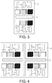
- the figure 3 represents a first variant of this component.
- the electronic component 20 comprises two triplets of three light-emitting diodes 21, 22 and 23; and 31, 32 and 33 and seven electrical contacts 24-26, 34-36 and 27, each light-emitting diode having a dedicated electrical control contact, the six diodes having a common electrical contact 27 to the six light-emitting diodes.
- the geometric implantation of light-emitting diodes and electrical contacts of the figure 3 is given as an example.
- the component has five fewer contacts.
- the size of the unit component is approximately 600 ⁇ m x 300 ⁇ m. Divide the previous carry-over time by two more times.
- the figure 4 represents a second variant of this component.
- the electronic component 40 comprises four triplets of three light-emitting diodes 41-43, 51-53, 61-63 and 71-73 and 13 electrical contacts 44-46, 54-56, 64-66, 74-76 and 47, each diode electroluminescent having a dedicated electrical control contact, the twelve diodes having a common electrical contact 47 to the twelve light emitting diodes.
- the geometric implantation of light-emitting diodes and electrical contacts of the figure 4 is given as an example.
- the size of the unit component is approximately 600 ⁇ m x 600 ⁇ m.
- the component has eleven fewer contacts. This type of component makes it possible to divide by twelve the delay time of a color screen. For a "full HD" display, it is necessary to report 518 400 elementary components, which can be achieved in 8.64 hours on a fast report machine with 60000 components per hour.
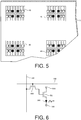
- this type of component 40 makes it possible to produce large screens with a surface of light-emitting diodes on a reduced sapphire substrate, typically of the order of 10% of the surface area. of the active matrix glass 1.
- the components are implanted every millimeter.
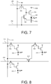
- the figure 6 represents the control electronics of a light emitting diode 300. This is located on the transparent plate near the intersections between the various lines 200 and 100 columns.
- the first transistor 400 is connected to the control column 100 and to the control line 200. It drives the transistor 450 which controls the light-emitting diode 300.
- a line and a control column can be assigned to each light-emitting diode, making a total of six conductive control lines.
- the control can be achieved by means of a single line and three control columns, ie in total only four conductive control lines.
- an RGB LED triplet can be controlled by only two lines 210 and 220 and a single column 110, ie three conductive lines.
- the electronic device is as follows.
- the first diode 301 is conventionally controlled by an electronics with two transistors as described in FIG. figure 6 , the transistor 401 being connected to the line 210 and to the column 110.
- the second diode 302 is conventionally controlled by an electronics with two transistors, the transistor 402 being connected to the line 220 and the column 110.
- the third diode 303 also comprises a control electronics with two transistors but the transistor 403 is connected to a transistor 470 controlled by the column 110 and the line 220.
- the diode is connected to the control column 110 and to the two control lines 210 and 220.
- the operation of the triplet is as follows.
- the line 210 activates the diode 301, then the line 220 activates the diode 302.
- the simultaneous action of the lines 210 and 220 activates the diode 303.
- the column 110 presents the information corresponding to the diode 303 during the simultaneous activation two lines 210 and 220 then the information corresponding to the diode 301 during the activation of only the first line 210 and the information corresponding to the diode 302 during the activation only of the line 220.
- the reduction in the number of rows and columns reduces the metal surface of the active matrix and therefore promotes the transparency of the display.
- the above principles can be implemented to power an electronic component comprising four triplets of three diodes.
- the supply circuit comprises two rows and four columns.
- FIG. 9 The diagram of the corresponding electronic control circuit is represented in figure 9 . It comprises three lines 210, 211 and 212 and three columns 110, 111 and 112.
- a first triplet of diodes 301, 302 and 303 is connected on the one hand to the first control column 110, to the second control column 111 and to the third control column 112 and on the other hand to the first command line 210.
- the second triplet of diodes 304, 305 and 306 is connected on the one hand to the first control column 110, to the second control column 111 and the third control column 112 and secondly to the second control line 212.
- the third triplet of diodes 311, 312 and 313 is connected on the one hand to the first control column 110, the second control column 111 and the third control column 112 and on the other hand to the first command line 210 and the third control line 211 by means of a first triplet of sample-and-hold devices 471, 472 and 473.
- Each sample-and-hold device is connected to a column, to the line 211 and to the transistor which drives the corresponding diode.
- the sample-and-hold circuit 471 is connected to the column 110, to the line 211 and to the transistor 411 which drives the diode 311.
- the fourth triplet of diodes 314, 315 and 316 is connected firstly to the first control column 110, to the second control column 111 and to the third control column 112 and secondly to the second control line 212 and the third control line 212 by means of a second triplet of sample-and-hold devices 474, 475 and 476.
- the diodes 311 to 316 comprising a sample-and-hold device are systematically activated before the diodes 301 to 306.
- the lines 210 and 211 are activated simultaneously before the activation of the line 210 only and, likewise, the lines 211 and 212 are activated simultaneously before activation of line 212 alone.
- sample-and-hold transistors 471 to 476 are connected differently.
- Each sample-and-hold device is connected to a first control transistor, to the line 211 and to the second transistor which drives the corresponding diode.
- the sample-and-hold circuit 471 is connected to the transistor 411, to the line 211 and to the second transistor which drives the diode 311.
- the transistor closest electrically to the column must be last blocked so as to reduce the emitting line-diode coupling.
- the portions of the electrodes of the transparent substrate disposed beneath the components may be reflective so as to promote the emission of light emitted by the light-emitting diodes to the user. he It is preferable that the surface of the control electronics of the components according to the invention is completely masked by the component itself so as to optimize the transmission of the display.
- the transfer of the components according to the invention to the transparent strip comprising the control lines and columns and the associated control electronics can be achieved by means of a conductive glue.
- the contacts 81 of the component 80 are fixed on the contacts 82 of the control electronics 85 by means of pads 83 of conductive glue.
- the control electronics is shown schematically in this figure and the following.
- the light emitting diodes are not shown.
- This conductive adhesive is isotropic. It is of the type solder paste or its equivalent. For example, it is arranged on the contacts of the active matrix by screen printing and then heat polymerized.
- the contacts 81 of the component 80 are fixed on the contacts 82 of the control electronics 85 by means of a single pad 83 of conductive glue.
- This conductive adhesive is anisotropic. It contains an insulating medium comprising disjoint conductive elements 84. These elements may be microbeads coated with gold or another metal. As before, each pad can be deposited by screen printing. It is also possible to use a tape glue containing the metal-coated microbeads, the tape being of the "ACF” type, which stands for "Anisotropic Conductive Film”. This glue is then laminated strip on the glass. These different glues are polymerized hot or under ultraviolet and under pressure.
- These mounting methods can be applied to components comprising a triplet of light-emitting diodes or two triplets or four triplets. Furthermore, it is preferable that the material used for the bonding is opaque so as to reduce the amount of light that propagates towards the control transistors whose operation could be disturbed by this light.
Landscapes
- Engineering & Computer Science (AREA)
- Physics & Mathematics (AREA)
- Computer Hardware Design (AREA)
- General Physics & Mathematics (AREA)
- Theoretical Computer Science (AREA)
- Devices For Indicating Variable Information By Combining Individual Elements (AREA)
- Chemical & Material Sciences (AREA)
- Inorganic Chemistry (AREA)
- Led Device Packages (AREA)
- Electroluminescent Light Sources (AREA)
- Control Of Indicators Other Than Cathode Ray Tubes (AREA)
Abstract
Description
- Le domaine de l'invention est celui des dispositifs de visualisation transparents qui permettent d'afficher une image ou des informations en superposition sur l'extérieur. On peut notamment les utiliser dans le domaine automobile ou en aéronautique.
- Un afficheur transparent comporte une matrice de pixels émissifs colorés adressés par un ensemble de lignes et de colonnes conductrices. Chaque intersection de lignes et de colonnes comporte un pixel et son électronique d'adressage comme on le voit sur la
figure 1 . - Pour que l'écran conserve une bonne transparence, il suffit que l'ensemble des lignes, des colonnes, des pixels et de l'électronique associée n'occupe qu'une faible partie de l'écran.
- Les pixels émissifs peuvent être des diodes électroluminescentes ou « LED » qui présentent de nombreux avantages. On citera notamment une puissance émettrice importante, un faible encombrement et une fiabilité élevée.
- Dans ce cas, l'électronique de commande ou d'adressage comporte plusieurs transistors réalisés en couches minces. L'un au moins connecté à une ligne et une colonne réalise la mémorisation de l'information vidéo. Un second transistor connecté à une alimentation et à la diode électroluminescente contrôle le courant dans celle-ci. Celui-ci peut être disposé sous la diode de façon à réduire la surface occupée par la matrice de diodes.
- La façon la plus simple de réaliser cet écran transparent à diodes électroluminescentes est montrée sur la
figure 1 qui représente une vue partielle d'un écran implanté sur un substrat transparent 1. Chaque intersection de lignes 2 et de colonnes 3 d'adressage comporte une diode électroluminescente unique. Pour réaliser un afficheur couleur, on utilise trois types de diodes différentes 4, 5 et 6 émettant respectivement dans le rouge, le bleu et le vert. - Ce type d'écran a deux inconvénients importants. Si l'on veut réaliser un écran dit « Full HD », cet écran doit comporter 1080 lignes et 1920 colonnes. Chaque pixel coloré comporte alors trois diodes électroluminescentes élémentaires. Ainsi, l'écran comporte plus de 6 millions de diodes électroluminescentes. Si la machine de report des diodes est capable de reporter 60 000 composants à l'heure, il faut donc plus de 100 heures de report pour réaliser l'afficheur transparent.
- Par ailleurs, les composants à manipuler par la méthode dite « Pick and Place » sont de très petite taille. Typiquement, une diode électroluminescente a des dimensions voisines de 100 microns. Ce sont donc des composants difficiles à manipuler et à positionner avec précision sur de grandes surfaces. Par ailleurs, ils sont susceptibles de bouger pendant le processus de thermalisation nécessaire à la solidification du composé de collage qui assure également la conduction électrique.
- L'afficheur transparent selon l'invention diminue de façon sensible les inconvénients précédents. En effet, les diodes électroluminescentes sont regroupées au moins par triplet « RGB », acronyme signifiant « Red - Green - Blue », chaque triplet constituant un pixel coloré. Ainsi, on diminue le nombre de composants à reporter, on augmente leur taille et on diminue le nombre de lignes et de colonnes d'adressage. L'afficheur demande moins de temps de réalisation, il est plus facile à réaliser, plus fiable et plus transparent.
- Plus précisément, l'invention a pour objet un afficheur comportant une lame transparente et une matrice de pixels composés de diodes électroluminescentes disposée sur ladite lame, caractérisé en ce que chaque pixel est un composant électronique comportant un triplet de trois diodes électroluminescentes émettant dans trois spectres différents et quatre contacts électriques, les trois diodes électroluminescentes étant réalisées sur un même substrat, chaque diode électroluminescente ayant un contact électrique de commande dédié, les trois diodes ayant un contact électrique commun auxdites trois diodes électroluminescentes, la surface occupée par la matrice de pixels étant d'un ordre de grandeur inférieur à celle de la lame transparente.
- Avantageusement, chaque composant électronique comporte deux triplets de trois diodes électroluminescentes et sept contacts électriques, chaque diode électroluminescente ayant un contact électrique de commande dédié, les deux triplets de trois diodes électroluminescentes étant réalisés sur le même substrat, les six diodes ayant un contact électrique commun auxdites six diodes électroluminescentes, la surface occupée par la matrice de pixels étant d'un ordre de grandeur inférieur à celle de la lame transparente.
- Avantageusement, chaque composant électronique comporte quatre triplets de trois diodes électroluminescentes et treize contacts électriques, les quatre triplets de trois diodes électroluminescentes étant réalisés sur le même substrat, chaque diode électroluminescente ayant un contact électrique de commande dédié, les douze diodes ayant un contact électrique commun auxdites douze diodes électroluminescentes, la surface occupée par la matrice de pixels étant d'un ordre de grandeur inférieur à celle de la lame transparente.
- Avantageusement, le substrat est du saphir, de carbure de silicium ou du silicium.
- Avantageusement, la lame transparente comportant un ensemble de lignes de commande et un ensemble de colonnes de commande, pour chaque triplet de diodes, le premier contact électrique de commande est relié à une première ligne, le second contact électrique de commande est relié à une seconde ligne, le troisième contact électrique de commande est relié à la première ligne et à la seconde ligne au moyen d'un échantillonneur bloqueur.
- Avantageusement, la lame transparente comportant un ensemble de lignes de commande et un ensemble de colonnes de commande,
- Le premier triplet de diodes est relié d'une part à une première colonne de commande, une seconde colonne de commande et une troisième colonne de commande et d'autre part à une première ligne de commande ;
- Le second triplet de diodes est relié d'une part à ladite première colonne de commande, à ladite seconde colonne de commande et à ladite troisième colonne de commande et d'autre part à une seconde ligne de commande ;
- Le troisième triplet de diodes est relié d'une part à ladite première colonne de commande, à la dite seconde colonne de commande et à ladite troisième colonne de commande et d'autre part à la dite première ligne de commande et à une troisième ligne de commande au moyen d'un premier triplet d'échantillonneurs bloqueurs ;
- Le quatrième triplet de diodes est relié d'une part à ladite première colonne de commande, à la dite seconde colonne de commande et à ladite troisième colonne de commande et d'autre part à la dite seconde ligne de commande et à ladite troisième ligne de commande au moyen d'un second triplet d'échantillonneurs bloqueurs.
- Avantageusement, chaque échantillonneur bloqueur est commandé par la troisième ligne et par une des trois colonnes de commande.
- Avantageusement, la surface d'implantation du composant électronique est d'environ 300 microns par 300 microns dans le cas d'un triplet de diodes, d'environ 300 microns par 600 microns dans le cas de deux triplets et de 600 microns par 600 microns dans le cas de quatre triplets de diodes électroluminescentes.
- L'invention concerne également un procédé de réalisation d'un afficheur comme défini ci-dessus, caractérisé en ce que le procédé comporte une étape de collage des composants électroniques sur des plots de collage, la colle étant conductrice, isotrope et du type pâte à braser.
- Avantageusement, dans une variante de réalisation, l'étape de collage est réalisée au moyen d'un film de collage conducteur du type « Anisotropic Conductive Film », la colle étant anisotrope, composée d'un milieu isolant comportant des microbilles conductrices.
- L'invention sera mieux comprise et d'autres avantages apparaîtront à la lecture de la description qui va suivre donnée à titre non limitatif et grâce aux figures annexées parmi lesquelles :
- La
figure 1 précédemment commentée représente un écran transparent selon l'art antérieur ; - La
figure 2 représente un triplet de diodes électroluminescentes selon l'invention ; - La
figure 3 représente deux triplets de diodes électroluminescentes selon l'invention ; - La
figure 4 représente quatre triplets de diodes électroluminescentes selon l'invention ; - La
figure 5 représente l'implantation des composants à quatre triplets de diodes sur un écran transparent ; - La
figure 6 représente le circuit électrique de commande d'une diode électroluminescente ; - La
figure 7 représente une variante du circuit électrique de commande de lafigure 6 ; - La
figure 8 représente le circuit électrique de commande d'un triplet de diodes électroluminescentes selon l'invention ; - La
figure 9 représente le circuit électrique de commande d'un composant comportant quatre triplets de diodes électroluminescentes selon l'invention ; - La
figure 10 représente une variante du circuit électrique de commande de lafigure 9 ; - La
figure 11 représente le montage des composants à diodes électroluminescentes selon l'invention sur leur substrat transparent ; - La
figure 12 représente une variante du montage des composants de lafigure 11 . - La
figure 2 représente un triplet de diodes électroluminescentes selon l'invention. Il se présente sous la forme d'un composant électronique 10. Ce composant comporte trois diodes électroluminescentes 11, 12 et 13 émettant respectivement dans le rouge, le vert et le bleu. Ces diodes électroluminescentes peuvent être, à titre d'exemple, émettre les différentes couleurs en natif ou émettre les différentes couleurs par conversion soit avec des phosphores soit avec des « quantum dots ». En particulier, la couleur bleue peut être obtenue en émission directe ou être le fruit d'une conversion par un phosphore approprié ou des quantum dots à partir d'un rayonnement ultraviolet d'émission. - Les trois diodes sont réalisées sur le même substrat. A titre d'exemples, ce substrat peut être du saphir, du carbure de silicium ou du silicium.
- Sur la
figure 2 , à titre d'exemple non limitatif, ces diodes électroluminescentes sont alignées. Ce composant comporte également quatre contacts électriques 14, 15, 16 et 17. Chaque diode électroluminescente a un contact électrique de commande dédié, les trois diodes ayant un contact électrique d'alimentation commun 17. Ainsi, par rapport à trois diodes unitaires, le composant comporte deux contacts de moins. La taille de chaque diode est d'environ 80µm x 120µm. Les dimensions de chaque contact ou « bump » sont environ 30µm x 80µm. La taille du composant unitaire est d'environ 300µm x 300µm. Cette taille se rapproche des standards de l'industrie de report des composants électroniques et permet de diviser par trois l'opération de report tout en la facilitant. - La
figure 3 représente une première variante de ce composant. Le composant électronique 20 comporte deux triplets de trois diodes électroluminescentes 21, 22 et 23 ; et 31, 32 et 33 et sept contacts électriques 24-26, 34-36 et 27, chaque diode électroluminescente ayant un contact électrique de commande dédié, les six diodes ayant un contact électrique commun 27 aux six diodes électroluminescentes. L'implantation géométrique des diodes électroluminescentes et des contacts électriques de lafigure 3 est donnée à titre d'exemple. Ainsi, par rapport à six diodes unitaires, le composant comporte cinq contacts de moins. La taille du composant unitaire est d'environ 600µm x 300µm. On divise une nouvelle fois par deux le temps de report précédent. - La
figure 4 représente une seconde variante de ce composant. Le composant électronique 40 comporte quatre triplets de trois diodes électroluminescentes 41-43, 51-53, 61-63 et 71-73 et 13 contacts électriques 44-46, 54-56, 64-66, 74-76 et 47, chaque diode électroluminescente ayant un contact électrique de commande dédié, les douze diodes ayant un contact électrique commun 47 aux douze diodes électroluminescentes. L'implantation géométrique des diodes électroluminescentes et des contacts électriques de lafigure 4 est donnée à titre d'exemple. La taille du composant unitaire est d'environ 600µm x 600µm. Ainsi, par rapport à douze diodes unitaires, le composant comporte onze contacts de moins. Ce type de composant permet de diviser par douze le temps de report d'un écran couleur. Pour un écran « full HD », il faut alors reporter 518 400 composants élémentaires, ce qui peut être réalisé en 8,64 heures sur une machine de report rapide à 60000 composants par heure. - Comme on le voit sur la
figure 5 qui représente une vue partielle d'un écran selon l'invention, ce type de composant 40 permet de réaliser des écrans de grande taille avec une surface de diodes électroluminescentes sur un substrat en saphir réduite typiquement de l'ordre de 10% de la surface du verre de la matrice active 1. Dans le cas de lafigure 5 , les composants sont implantés tous les millimètres. - La
figure 6 représente l'électronique de commande d'une diode électroluminescente 300. Celle-ci est implantée sur la lame transparente au voisinage des intersections entre les différentes lignes 200 et colonnes 100. - Elle comporte deux plans d'alimentation électrique notés classiquement « VDD » et « VSS » sur la
figure 6 et deux transistors de commande 400 et 450. Le premier transistor 400 est connecté à la colonne de commande 100 et à la ligne de commande 200. Il pilote le transistor 450 qui commande la diode électroluminescente 300. - Le dispositif de commande de la LED peut être réalisé avec un plus grand nombre de transistors pour améliorer les performances de l'afficheur. On citera :
- L'ajout de transistors de compensation des variations des caractéristiques électriques entre les diodes ou entre les transistors pour compenser les tensions de seuil ;
- L'ajout d'un transistor 460 dit de RESET, tel que représenté sur la
figure 7 . On utilise les mêmes notations dans cette figure que dans la précédente. Ce transistor est connecté à une ligne dite de « reset » 250, au transistor 450 et au plan d'alimentation VSS. Il permet de diminuer le temps d'activation des diodes, de façon à autoriser une réduction de l'émission de lumière lorsque l'afficheur est utilisé dans un environnement sombre. - Pour commander un triplet de diodes électroluminescentes, on peut affecter une ligne et une colonne de commande à chaque diode électroluminescente, soit au total six lignes conductrices de commande. Cependant, dans le cas d'un triplet de diodes selon l'invention, la commande peut être réalisée au moyen d'une seule ligne et de trois colonnes de commande, soit au total seulement quatre lignes conductrices de commande.
- On peut encore diminuer le nombre de lignes conductrices nécessaires pour le pilotage d'un triplet de diodes selon l'invention comme on le voit sur le schéma électrique de la
figure 8 . Dans ce cas, un triplet de LED RGB peut être commandé par uniquement deux lignes 210 et 220 et une seule colonne 110, soit trois lignes conductrices. - Le dispositif électronique est le suivant. La première diode 301 est commandée classiquement par une électronique à deux transistors telle que décrite en
figure 6 , le transistor 401 étant relié à la ligne 210 et à la colonne 110. De la même façon, la seconde diode 302 est commandée classiquement par une électronique à deux transistors, le transistor 402 étant relié à la ligne 220 et à la colonne 110. La troisième diode 303 comporte également une électronique de commande à deux transistors mais le transistor 403 est relié à un transistor 470 commandé par la colonne 110 et la ligne 220. Ainsi, au moyen des transistors 402 et 470, la diode est connectée à la colonne de commande 110 et aux deux lignes de commande 210 et 220. - Le fonctionnement du triplet est le suivant. La ligne 210 active la diode 301, puis la ligne 220 active la diode 302. Enfin, l'action simultanée des lignes 210 et 220 active la diode 303. La colonne 110 présente l'information correspondant à la diode 303 pendant l'activation simultanée des deux lignes 210 et 220 puis l'information correspondant à la diode 301 pendant l'activation uniquement de la première ligne 210 et l'information correspondant à la diode 302 pendant l'activation uniquement de la ligne 220.
- La réduction du nombre de lignes et de colonnes permet de réduire la surface de métal de la matrice active et donc favorise la transparence de l'afficheur.
- Les principes précédents peuvent être mis en oeuvre pour alimenter un composant électronique comportant quatre triplets de trois diodes. Dans ce cas, le circuit d'alimentation comprend deux lignes et quatre colonnes.
- Dans une variante de réalisation, il est possible d'alimenter un composant comportant douze diodes au moyen de trois lignes et de trois colonnes de commande. Le schéma du circuit électronique de commande correspondant est représenté en
figure 9 . Il comporte trois lignes 210, 211 et 212 et trois colonnes 110, 111 et 112. - Un premier triplet de diodes 301, 302 et 303 est relié d'une part à la première colonne de commande 110, à la seconde colonne de commande 111 et à la troisième colonne de commande 112 et d'autre part à la première ligne de commande 210.
- Le second triplet de diodes 304, 305 et 306 est relié d'une part à la première colonne de commande 110, à la seconde colonne de commande 111 et à la troisième colonne de commande 112 et d'autre part à la seconde ligne de commande 212.
- Le troisième triplet de diodes 311, 312 et 313 est relié d'une part à la première colonne de commande 110, à la seconde colonne de commande 111 et à la troisième colonne de commande 112 et d'autre part à la première ligne de commande 210 et à la troisième ligne de commande 211 au moyen d'un premier triplet d'échantillonneurs bloqueurs 471, 472 et 473. Chaque échantillonneur bloqueur est relié à une colonne, à la ligne 211 et au transistor qui pilote la diode correspondante. Ainsi, l'échantillonneur bloqueur 471 est relié à la colonne 110, à la ligne 211 et au transistor 411 qui pilote la diode 311.
- Le quatrième triplet de diodes 314, 315 et 316 est relié d'une part à la première colonne de commande 110, à la seconde colonne de commande 111 et à la troisième colonne de commande 112 et d'autre part à la seconde ligne de commande 212 et à la troisième ligne de commande 212 au moyen d'un second triplet d'échantillonneurs bloqueurs 474, 475 et 476.
- Les diodes 311 à 316 comportant un échantillonneur bloqueur sont systématiquement activées avant les diodes 301 à 306. Les lignes 210 et 211 sont activées simultanément avant l'activation de la ligne 210 seule et, de même, les lignes 211 et 212 sont activées simultanément avant l'activation de la ligne 212 seule.
- Dans une variante de réalisation représentée en
figure 10 du circuit électronique d'adressage de lafigure 9 , les transistors échantillonneurs bloqueurs 471 à 476 sont raccordés différemment. Chaque échantillonneur bloqueur est relié à un premier transistor de commande, à la ligne 211 et au second transistor qui pilote la diode correspondante. Ainsi, l'échantillonneur bloqueur 471 est relié au transistor 411, à la ligne 211 et au second transistor qui pilote la diode 311. - Dans tous les cas de commande des diodes avec deux transistors en série dans les échantillonneurs bloqueurs, le transistor le plus proche électriquement de la colonne doit être bloqué en dernier de façon à réduire le couplage ligne-diode émettrice.
- Les parties des électrodes du substrat transparent disposées sous les composants peuvent être réfléchissantes de façon à favoriser l'émission de la lumière émise par les diodes électroluminescentes vers l'utilisateur. Il est préférable que la surface de l'électronique de commande des composants selon l'invention soit totalement masquée par le composant lui-même de façon à optimiser la transmission de l'afficheur.
- Le report des composants selon l'invention sur la lame transparente comportant les lignes et les colonnes de commande et l'électronique de commande associée peut être réalisé au moyen d'une colle conductrice.
- Dans un premier mode de réalisation représenté sur la
figure 11 , les contacts 81 du composant 80 sont fixés sur les contacts 82 de l'électronique de commande 85 au moyen de plots 83 de colle conductrice. L'électronique de commande est représentée de façon simplifiée sur cette figure et la suivante. Sur cettefigure 11 et la suivante, les diodes électroluminescentes ne sont pas représentées. Cette colle conductrice est isotrope. Elle est du type pâte à braser ou son équivalent. A titre d'exemple, elle est disposée sur les contacts de la matrice active par sérigraphie puis polymérisée à chaud. - Dans un second mode de réalisation représenté sur la
figure 12 , les contacts 81 du composant 80 sont fixés sur les contacts 82 de l'électronique de commande 85 au moyen d'un plot unique 83 de colle conductrice. Cette colle conductrice est anisotrope. Elle contient un milieu isolant comportant des éléments conducteurs disjoints 84. Ces éléments peuvent être des microbilles revêtues d'or ou d'un autre métal. Comme précédemment, chaque plot peut être déposé par sérigraphie. On peut également utiliser une colle en ruban contenant les microbilles à revêtement métallique, le ruban étant du type « ACF », acronyme de « Anisotropic Conductive Film ». Cette colle est alors laminée en bande sur le verre. Ces différentes colles sont polymérisées à chaud ou sous ultraviolet et sous pression. - Ces méthodes de montage peuvent s'appliquer à des composants comportant un triplet de diodes électroluminescentes ou deux triplets ou quatre triplets. Par ailleurs, il est préférable que le matériau utilisé pour le collage soit opaque de façon à réduire la quantité de lumière qui se propage vers les transistors de commande dont le fonctionnement pourrait être perturbé par cette lumière.
Claims (12)
- Afficheur comportant une lame transparente (1) et une matrice de pixels composés de diodes électroluminescentes disposée sur ladite lame, caractérisé en ce que chaque pixel est un composant électronique (10) comportant un triplet de trois diodes électroluminescentes (11-13) émettant dans trois spectres différents et quatre contacts électriques (14-17), les trois diodes électroluminescentes étant réalisées sur un même substrat, chaque diode électroluminescente ayant un contact électrique (14-16) de commande dédié, les trois diodes ayant un contact électrique (17) commun auxdites trois diodes électroluminescentes, la surface occupée par la matrice de pixels étant d'un ordre de grandeur inférieur à celle de la lame transparente.
- Afficheur selon la revendication 1, caractérisé en ce que chaque composant électronique (20) comporte deux triplets de trois diodes électroluminescentes (21-23, 31-33) et sept contacts électriques (24-27, 34-36), les deux triplets de trois diodes électroluminescentes étant réalisés sur le même substrat, chaque diode électroluminescente ayant un contact électrique de commande dédié (24-26, 34-36), les six diodes ayant un contact électrique commun (27) auxdites six diodes électroluminescentes, la surface occupée par la matrice de pixels étant d'un ordre de grandeur inférieur à celle de la lame transparente.
- Afficheur selon la revendication 2, caractérisé en ce que chaque composant électronique (40) comporte quatre triplets de trois diodes électroluminescentes (41-43, 51-53, 61-63, 71-73) et treize contacts électriques (44-47, 54-56, 64-66, 74-76), les quatre triplets de trois diodes électroluminescentes étant réalisés sur le même substrat, chaque diode électroluminescente ayant un contact électrique (44-46, 54-56, 64-66, 74-76) de commande dédié, les douze diodes ayant un contact électrique commun (47) auxdites douze diodes électroluminescentes, la surface occupée par la matrice de pixels étant d'un ordre de grandeur inférieur à celle de la lame transparente.
- Afficheur selon l'une des revendications précédentes, caractérisé en ce que le substrat est du saphir, de carbure de silicium ou du silicium.
- Afficheur selon l'une des revendications précédentes, caractérisé en ce que, la lame transparente comportant un ensemble de lignes de commande (210, 220) et un ensemble de colonnes de commande (110), pour chaque triplet de diodes, le premier contact électrique de commande est relié à une première ligne (210), le second contact électrique de commande est relié à une seconde ligne (220), le troisième contact électrique de commande est relié à la première ligne et à la seconde ligne au moyen d'un échantillonneur bloqueur.
- Afficheur selon la revendication 3, caractérisé en ce que, la lame transparente comportant un ensemble de lignes de commande (210, 211, 212) et un ensemble de colonnes de commande (110, 111, 112),Le premier triplet de diodes (301-303) est relié d'une part à une première colonne de commande (110), une seconde colonne de commande (111) et une troisième colonne de commande (112) et d'autre part à une première ligne de commande (210) ;Le second triplet de diodes (304-306) est relié d'une part à ladite première colonne de commande (110), à ladite seconde colonne de commande (111) et à ladite troisième colonne de commande (112) et d'autre part à une seconde ligne de commande (212) ;Le troisième triplet de diodes (311-313) est relié d'une part à ladite première colonne de commande (110), à la dite seconde colonne de commande (111) et à ladite troisième colonne de commande (112) et d'autre part à la dite première ligne de commande (210) et à une troisième ligne de commande (211) au moyen d'un premier triplet d'échantillonneurs bloqueurs (471-473) ;Le quatrième triplet de diodes (314-316) est relié d'une part à ladite première colonne de commande (110), à la dite seconde colonne de commande (111) et à ladite troisième colonne de commande (112) et d'autre part à la dite seconde ligne de commande (212) et à ladite troisième ligne de commande (211) au moyen d'un second triplet d'échantillonneurs bloqueurs (474-476).
- Afficheur selon la revendication 6, caractérisé en ce que chaque échantillonneur bloqueur est commandé par la troisième ligne et par une des trois colonnes de commande.
- Afficheur selon la revendication 1, caractérisé en ce que la surface d'implantation du composant électronique (10) est d'environ 300 microns par 300 microns.
- Afficheur selon la revendication 2, caractérisé en ce que la surface d'implantation du composant électronique (20) est d'environ 300 microns par 600 microns.
- Afficheur selon la revendication 3, caractérisé en ce que la surface d'implantation du composant électronique (40) est d'environ 600 microns par 600 microns.
- Procédé de réalisation d'un afficheur selon l'une des revendications précédentes, caractérisé en ce qu'il comporte une étape de collage des composants électroniques sur des plots de collage (83), la colle étant conductrice, isotrope et du type pâte à braser.
- Procédé de réalisation d'un afficheur selon l'une des revendications 1 à 10, caractérisé en ce qu'il comporte une étape de collage des composants électroniques au moyen d'un film de collage (83) conducteur du type « Anisotropic Conductive Film », la colle étant anisotrope, composée d'un milieu isolant comportant des microbilles conductrices (84).
Applications Claiming Priority (1)
| Application Number | Priority Date | Filing Date | Title |
|---|---|---|---|
| FR1700754A FR3069089B1 (fr) | 2017-07-13 | 2017-07-13 | Afficheur transparent a matrice active comportant des pixels emissifs a diodes electroluminescentes colorees |
Publications (2)
| Publication Number | Publication Date |
|---|---|
| EP3428908A1 true EP3428908A1 (fr) | 2019-01-16 |
| EP3428908B1 EP3428908B1 (fr) | 2021-11-17 |
Family
ID=60955075
Family Applications (1)
| Application Number | Title | Priority Date | Filing Date |
|---|---|---|---|
| EP18182512.6A Active EP3428908B1 (fr) | 2017-07-13 | 2018-07-09 | Afficheur transparent a matrice active comportant des pixels emissifs a diodes electroluminescentes colorees |
Country Status (7)
| Country | Link |
|---|---|
| US (1) | US20190019781A1 (fr) |
| EP (1) | EP3428908B1 (fr) |
| JP (1) | JP2019032514A (fr) |
| KR (1) | KR20190008124A (fr) |
| CN (1) | CN109273435A (fr) |
| FR (1) | FR3069089B1 (fr) |
| TW (1) | TW201909407A (fr) |
Families Citing this family (7)
| Publication number | Priority date | Publication date | Assignee | Title |
|---|---|---|---|---|
| US11038088B2 (en) | 2019-10-14 | 2021-06-15 | Lextar Electronics Corporation | Light emitting diode package |
| EP4379802A4 (fr) | 2021-12-02 | 2024-12-25 | Samsung Electronics Co., Ltd. | Module d'affichage et appareil d'affichage le comprenant |
| KR102891668B1 (ko) * | 2021-12-02 | 2025-11-27 | 삼성전자주식회사 | 디스플레이 모듈 및 이를 포함하는 디스플레이 장치 |
| KR20250161637A (ko) * | 2022-06-02 | 2025-11-17 | 엘지전자 주식회사 | 반도체 발광 소자를 이용한 디스플레이 장치 |
| KR20250038551A (ko) | 2023-09-12 | 2025-03-19 | 딜라이트 글로벌 씨오., 엘티디. | 투명 표시 장치 |
| KR20250038552A (ko) | 2023-09-12 | 2025-03-19 | 딜라이트 글로벌 씨오., 엘티디. | 투명 표시 장치 |
| KR20250046878A (ko) | 2023-09-27 | 2025-04-03 | 딜라이트 글로벌 씨오., 엘티디. | 단차 보정 가능한 표시 장치 |
Citations (6)
| Publication number | Priority date | Publication date | Assignee | Title |
|---|---|---|---|---|
| US20060001625A1 (en) * | 2004-07-02 | 2006-01-05 | Tsinghua University | Double-faced light emiting diode display |
| US20080218465A1 (en) * | 2007-03-05 | 2008-09-11 | Chunghwa Picture Tubes, Ltd. | Display panel, display apparatus and driving method thereof |
| US20090283781A1 (en) * | 2008-05-16 | 2009-11-19 | Cree Hong Kong Limited | Mini V SMD |
| US20120223875A1 (en) * | 2009-12-09 | 2012-09-06 | Nano And Advanced Materials Institute Limited | Monolithic full-color led micro-display on an active matrix panel manufactured using flip-chip technology |
| US20140353694A1 (en) * | 2013-05-29 | 2014-12-04 | Cree Huizhou Solid State Lighting Company Limited | Multiple pixel surface mount device package |
| US20150371585A1 (en) * | 2014-06-18 | 2015-12-24 | X-Celeprint Limited | Micro assembled led displays and lighting elements |
Family Cites Families (20)
| Publication number | Priority date | Publication date | Assignee | Title |
|---|---|---|---|---|
| TW548615B (en) * | 2002-03-29 | 2003-08-21 | Chi Mei Optoelectronics Corp | Display panel having driver circuit with data line commonly used by three adjacent pixels |
| US8947619B2 (en) * | 2006-07-06 | 2015-02-03 | Intematix Corporation | Photoluminescence color display comprising quantum dots material and a wavelength selective filter that allows passage of excitation radiation and prevents passage of light generated by photoluminescence materials |
| KR101563692B1 (ko) * | 2007-10-19 | 2015-10-27 | 가부시키가이샤 한도오따이 에네루기 켄큐쇼 | 표시장치 및 그 구동 방법 |
| JP2009157015A (ja) * | 2007-12-26 | 2009-07-16 | Komaden:Kk | Led表示装置及びled表示ユニット |
| CN102024387B (zh) * | 2009-09-18 | 2013-06-12 | 深圳市晶泓科技有限公司 | 一种高透明led显示模块 |
| JP5370264B2 (ja) * | 2010-05-20 | 2013-12-18 | カシオ計算機株式会社 | 表示装置 |
| JP5652100B2 (ja) * | 2010-10-05 | 2015-01-14 | ソニー株式会社 | 表示パネル、表示装置、照明パネルおよび照明装置、ならびに表示パネルおよび照明パネルの製造方法 |
| TW201229653A (en) * | 2010-12-31 | 2012-07-16 | Bascule Dev Ag Llc | Transmitting color image projector and the method thereof |
| KR101442705B1 (ko) * | 2012-10-18 | 2014-09-19 | 지스마트 주식회사 | 균일한 광출력이 가능한 투명전광판 |
| JP2015166756A (ja) * | 2014-03-03 | 2015-09-24 | 株式会社ラパンクリエイト | 表示ユニットおよび表示装置 |
| TWI556478B (zh) * | 2014-06-30 | 2016-11-01 | 億光電子工業股份有限公司 | 發光二極體裝置 |
| US9799261B2 (en) * | 2014-09-25 | 2017-10-24 | X-Celeprint Limited | Self-compensating circuit for faulty display pixels |
| CN104820326B (zh) * | 2015-05-28 | 2017-11-28 | 京东方科技集团股份有限公司 | 阵列基板、显示面板、显示装置及驱动方法 |
| US10102794B2 (en) * | 2015-06-09 | 2018-10-16 | X-Celeprint Limited | Distributed charge-pump power-supply system |
| CN104979326B (zh) * | 2015-07-09 | 2017-12-05 | 深圳市晶泓科技有限公司 | Led发光组件、led发光面板和led显示屏 |
| CN104934008A (zh) * | 2015-07-09 | 2015-09-23 | 京东方科技集团股份有限公司 | 一种阵列基板及其驱动方法、显示面板、显示装置 |
| JP6995739B2 (ja) * | 2015-07-23 | 2022-01-17 | ソウル セミコンダクター カンパニー リミテッド | ディスプレイ装置及びその製造方法 |
| KR102609932B1 (ko) * | 2015-09-09 | 2023-12-04 | 이노럭스 코포레이션 | 디스플레이 디바이스 |
| US9930277B2 (en) * | 2015-12-23 | 2018-03-27 | X-Celeprint Limited | Serial row-select matrix-addressed system |
| US10832609B2 (en) * | 2017-01-10 | 2020-11-10 | X Display Company Technology Limited | Digital-drive pulse-width-modulated output system |
-
2017
- 2017-07-13 FR FR1700754A patent/FR3069089B1/fr active Active
-
2018
- 2018-07-09 EP EP18182512.6A patent/EP3428908B1/fr active Active
- 2018-07-10 TW TW107123869A patent/TW201909407A/zh unknown
- 2018-07-10 JP JP2018130656A patent/JP2019032514A/ja active Pending
- 2018-07-11 KR KR1020180080787A patent/KR20190008124A/ko not_active Ceased
- 2018-07-12 US US16/034,306 patent/US20190019781A1/en not_active Abandoned
- 2018-07-13 CN CN201810769029.4A patent/CN109273435A/zh active Pending
Patent Citations (6)
| Publication number | Priority date | Publication date | Assignee | Title |
|---|---|---|---|---|
| US20060001625A1 (en) * | 2004-07-02 | 2006-01-05 | Tsinghua University | Double-faced light emiting diode display |
| US20080218465A1 (en) * | 2007-03-05 | 2008-09-11 | Chunghwa Picture Tubes, Ltd. | Display panel, display apparatus and driving method thereof |
| US20090283781A1 (en) * | 2008-05-16 | 2009-11-19 | Cree Hong Kong Limited | Mini V SMD |
| US20120223875A1 (en) * | 2009-12-09 | 2012-09-06 | Nano And Advanced Materials Institute Limited | Monolithic full-color led micro-display on an active matrix panel manufactured using flip-chip technology |
| US20140353694A1 (en) * | 2013-05-29 | 2014-12-04 | Cree Huizhou Solid State Lighting Company Limited | Multiple pixel surface mount device package |
| US20150371585A1 (en) * | 2014-06-18 | 2015-12-24 | X-Celeprint Limited | Micro assembled led displays and lighting elements |
Also Published As
| Publication number | Publication date |
|---|---|
| CN109273435A (zh) | 2019-01-25 |
| KR20190008124A (ko) | 2019-01-23 |
| FR3069089B1 (fr) | 2019-08-09 |
| FR3069089A1 (fr) | 2019-01-18 |
| TW201909407A (zh) | 2019-03-01 |
| US20190019781A1 (en) | 2019-01-17 |
| EP3428908B1 (fr) | 2021-11-17 |
| JP2019032514A (ja) | 2019-02-28 |
Similar Documents
| Publication | Publication Date | Title |
|---|---|---|
| EP3428908B1 (fr) | Afficheur transparent a matrice active comportant des pixels emissifs a diodes electroluminescentes colorees | |
| TWI677977B (zh) | Led單元、影像顯示元件及其製造方法 | |
| US10707265B2 (en) | Display devices | |
| US11538851B2 (en) | Display device and display device manufacturing method | |
| US20180158847A1 (en) | Light emitting diode display | |
| FR3069378B1 (fr) | Dispositif optoelectronique | |
| EP3815139B1 (fr) | Dispositif optoelectronique a diodes electroluminescentes | |
| EP3529834B1 (fr) | Dispositif d'affichage et procede de fabrication d'un tel dispositif | |
| US20200251460A1 (en) | Micro-led element, image display element, and production method | |
| FR3069379B1 (fr) | Dispositif optoelectronique | |
| FR3044467A1 (fr) | Dalle lumineuse et procede de fabrication d'une telle dalle lumineuse | |
| CN114762027A (zh) | 显示装置 | |
| US20220278260A1 (en) | Display apparatus using semiconductor light emitting device | |
| US20220406982A1 (en) | Display device using semiconductor light emitting elements, and method for manufacturing same | |
| US20230170353A1 (en) | Display apparatus, method of manufacturing display apparatus, and electronic apparatus | |
| CA2892450A1 (fr) | Ecran d'affichage a diodes electroluminescentes organiques | |
| US12266747B2 (en) | Light-emitting substrate, method for forming the light-emitting substrate and display device | |
| CN113924662B (zh) | 具有悬臂电极的发光元件、具有其的显示面板及显示装置 | |
| US20240162402A1 (en) | Display device | |
| EP3921871B1 (fr) | Dispositif d'affichage electroluminescent | |
| WO2021130073A1 (fr) | Afficheur a microleds a emission au travers de la matrice active | |
| WO2023126134A1 (fr) | Pixel d'affichage a diodes electroluminescentes pour ecran d'affichage | |
| CN120283306A (zh) | 显示器像素用层叠型半导体发光元件及包括该层叠型半导体发光元件的显示器装置 | |
| KR20210026848A (ko) | 도전성 캐리어 및 디스플레이 패널의 제조방법 |
Legal Events
| Date | Code | Title | Description |
|---|---|---|---|
| PUAI | Public reference made under article 153(3) epc to a published international application that has entered the european phase |
Free format text: ORIGINAL CODE: 0009012 |
|
| STAA | Information on the status of an ep patent application or granted ep patent |
Free format text: STATUS: THE APPLICATION HAS BEEN PUBLISHED |
|
| AK | Designated contracting states |
Kind code of ref document: A1 Designated state(s): AL AT BE BG CH CY CZ DE DK EE ES FI FR GB GR HR HU IE IS IT LI LT LU LV MC MK MT NL NO PL PT RO RS SE SI SK SM TR |
|
| AX | Request for extension of the european patent |
Extension state: BA ME |
|
| STAA | Information on the status of an ep patent application or granted ep patent |
Free format text: STATUS: REQUEST FOR EXAMINATION WAS MADE |
|
| 17P | Request for examination filed |
Effective date: 20190711 |
|
| RBV | Designated contracting states (corrected) |
Designated state(s): AL AT BE BG CH CY CZ DE DK EE ES FI FR GB GR HR HU IE IS IT LI LT LU LV MC MK MT NL NO PL PT RO RS SE SI SK SM TR |
|
| STAA | Information on the status of an ep patent application or granted ep patent |
Free format text: STATUS: EXAMINATION IS IN PROGRESS |
|
| 17Q | First examination report despatched |
Effective date: 20200218 |
|
| GRAP | Despatch of communication of intention to grant a patent |
Free format text: ORIGINAL CODE: EPIDOSNIGR1 |
|
| STAA | Information on the status of an ep patent application or granted ep patent |
Free format text: STATUS: GRANT OF PATENT IS INTENDED |
|
| INTG | Intention to grant announced |
Effective date: 20210630 |
|
| GRAS | Grant fee paid |
Free format text: ORIGINAL CODE: EPIDOSNIGR3 |
|
| GRAA | (expected) grant |
Free format text: ORIGINAL CODE: 0009210 |
|
| STAA | Information on the status of an ep patent application or granted ep patent |
Free format text: STATUS: THE PATENT HAS BEEN GRANTED |
|
| AK | Designated contracting states |
Kind code of ref document: B1 Designated state(s): AL AT BE BG CH CY CZ DE DK EE ES FI FR GB GR HR HU IE IS IT LI LT LU LV MC MK MT NL NO PL PT RO RS SE SI SK SM TR |
|
| REG | Reference to a national code |
Ref country code: GB Ref legal event code: FG4D Free format text: NOT ENGLISH |
|
| REG | Reference to a national code |
Ref country code: IE Ref legal event code: FG4D Free format text: LANGUAGE OF EP DOCUMENT: FRENCH |
|
| REG | Reference to a national code |
Ref country code: DE Ref legal event code: R096 Ref document number: 602018026723 Country of ref document: DE |
|
| REG | Reference to a national code |
Ref country code: AT Ref legal event code: REF Ref document number: 1448732 Country of ref document: AT Kind code of ref document: T Effective date: 20211215 |
|
| REG | Reference to a national code |
Ref country code: LT Ref legal event code: MG9D |
|
| REG | Reference to a national code |
Ref country code: NL Ref legal event code: MP Effective date: 20211117 |
|
| REG | Reference to a national code |
Ref country code: AT Ref legal event code: MK05 Ref document number: 1448732 Country of ref document: AT Kind code of ref document: T Effective date: 20211117 |
|
| PG25 | Lapsed in a contracting state [announced via postgrant information from national office to epo] |
Ref country code: RS Free format text: LAPSE BECAUSE OF FAILURE TO SUBMIT A TRANSLATION OF THE DESCRIPTION OR TO PAY THE FEE WITHIN THE PRESCRIBED TIME-LIMIT Effective date: 20211117 Ref country code: LT Free format text: LAPSE BECAUSE OF FAILURE TO SUBMIT A TRANSLATION OF THE DESCRIPTION OR TO PAY THE FEE WITHIN THE PRESCRIBED TIME-LIMIT Effective date: 20211117 Ref country code: FI Free format text: LAPSE BECAUSE OF FAILURE TO SUBMIT A TRANSLATION OF THE DESCRIPTION OR TO PAY THE FEE WITHIN THE PRESCRIBED TIME-LIMIT Effective date: 20211117 Ref country code: BG Free format text: LAPSE BECAUSE OF FAILURE TO SUBMIT A TRANSLATION OF THE DESCRIPTION OR TO PAY THE FEE WITHIN THE PRESCRIBED TIME-LIMIT Effective date: 20220217 Ref country code: AT Free format text: LAPSE BECAUSE OF FAILURE TO SUBMIT A TRANSLATION OF THE DESCRIPTION OR TO PAY THE FEE WITHIN THE PRESCRIBED TIME-LIMIT Effective date: 20211117 |
|
| PG25 | Lapsed in a contracting state [announced via postgrant information from national office to epo] |
Ref country code: IS Free format text: LAPSE BECAUSE OF FAILURE TO SUBMIT A TRANSLATION OF THE DESCRIPTION OR TO PAY THE FEE WITHIN THE PRESCRIBED TIME-LIMIT Effective date: 20220317 Ref country code: SE Free format text: LAPSE BECAUSE OF FAILURE TO SUBMIT A TRANSLATION OF THE DESCRIPTION OR TO PAY THE FEE WITHIN THE PRESCRIBED TIME-LIMIT Effective date: 20211117 Ref country code: PT Free format text: LAPSE BECAUSE OF FAILURE TO SUBMIT A TRANSLATION OF THE DESCRIPTION OR TO PAY THE FEE WITHIN THE PRESCRIBED TIME-LIMIT Effective date: 20220317 Ref country code: PL Free format text: LAPSE BECAUSE OF FAILURE TO SUBMIT A TRANSLATION OF THE DESCRIPTION OR TO PAY THE FEE WITHIN THE PRESCRIBED TIME-LIMIT Effective date: 20211117 Ref country code: NO Free format text: LAPSE BECAUSE OF FAILURE TO SUBMIT A TRANSLATION OF THE DESCRIPTION OR TO PAY THE FEE WITHIN THE PRESCRIBED TIME-LIMIT Effective date: 20220217 Ref country code: NL Free format text: LAPSE BECAUSE OF FAILURE TO SUBMIT A TRANSLATION OF THE DESCRIPTION OR TO PAY THE FEE WITHIN THE PRESCRIBED TIME-LIMIT Effective date: 20211117 Ref country code: LV Free format text: LAPSE BECAUSE OF FAILURE TO SUBMIT A TRANSLATION OF THE DESCRIPTION OR TO PAY THE FEE WITHIN THE PRESCRIBED TIME-LIMIT Effective date: 20211117 Ref country code: HR Free format text: LAPSE BECAUSE OF FAILURE TO SUBMIT A TRANSLATION OF THE DESCRIPTION OR TO PAY THE FEE WITHIN THE PRESCRIBED TIME-LIMIT Effective date: 20211117 Ref country code: GR Free format text: LAPSE BECAUSE OF FAILURE TO SUBMIT A TRANSLATION OF THE DESCRIPTION OR TO PAY THE FEE WITHIN THE PRESCRIBED TIME-LIMIT Effective date: 20220218 Ref country code: ES Free format text: LAPSE BECAUSE OF FAILURE TO SUBMIT A TRANSLATION OF THE DESCRIPTION OR TO PAY THE FEE WITHIN THE PRESCRIBED TIME-LIMIT Effective date: 20211117 |
|
| PG25 | Lapsed in a contracting state [announced via postgrant information from national office to epo] |
Ref country code: SM Free format text: LAPSE BECAUSE OF FAILURE TO SUBMIT A TRANSLATION OF THE DESCRIPTION OR TO PAY THE FEE WITHIN THE PRESCRIBED TIME-LIMIT Effective date: 20211117 Ref country code: SK Free format text: LAPSE BECAUSE OF FAILURE TO SUBMIT A TRANSLATION OF THE DESCRIPTION OR TO PAY THE FEE WITHIN THE PRESCRIBED TIME-LIMIT Effective date: 20211117 Ref country code: RO Free format text: LAPSE BECAUSE OF FAILURE TO SUBMIT A TRANSLATION OF THE DESCRIPTION OR TO PAY THE FEE WITHIN THE PRESCRIBED TIME-LIMIT Effective date: 20211117 Ref country code: EE Free format text: LAPSE BECAUSE OF FAILURE TO SUBMIT A TRANSLATION OF THE DESCRIPTION OR TO PAY THE FEE WITHIN THE PRESCRIBED TIME-LIMIT Effective date: 20211117 Ref country code: DK Free format text: LAPSE BECAUSE OF FAILURE TO SUBMIT A TRANSLATION OF THE DESCRIPTION OR TO PAY THE FEE WITHIN THE PRESCRIBED TIME-LIMIT Effective date: 20211117 Ref country code: CZ Free format text: LAPSE BECAUSE OF FAILURE TO SUBMIT A TRANSLATION OF THE DESCRIPTION OR TO PAY THE FEE WITHIN THE PRESCRIBED TIME-LIMIT Effective date: 20211117 |
|
| REG | Reference to a national code |
Ref country code: DE Ref legal event code: R097 Ref document number: 602018026723 Country of ref document: DE |
|
| PLBE | No opposition filed within time limit |
Free format text: ORIGINAL CODE: 0009261 |
|
| STAA | Information on the status of an ep patent application or granted ep patent |
Free format text: STATUS: NO OPPOSITION FILED WITHIN TIME LIMIT |
|
| 26N | No opposition filed |
Effective date: 20220818 |
|
| PG25 | Lapsed in a contracting state [announced via postgrant information from national office to epo] |
Ref country code: AL Free format text: LAPSE BECAUSE OF FAILURE TO SUBMIT A TRANSLATION OF THE DESCRIPTION OR TO PAY THE FEE WITHIN THE PRESCRIBED TIME-LIMIT Effective date: 20211117 |
|
| PG25 | Lapsed in a contracting state [announced via postgrant information from national office to epo] |
Ref country code: SI Free format text: LAPSE BECAUSE OF FAILURE TO SUBMIT A TRANSLATION OF THE DESCRIPTION OR TO PAY THE FEE WITHIN THE PRESCRIBED TIME-LIMIT Effective date: 20211117 |
|
| REG | Reference to a national code |
Ref country code: DE Ref legal event code: R119 Ref document number: 602018026723 Country of ref document: DE |
|
| PG25 | Lapsed in a contracting state [announced via postgrant information from national office to epo] |
Ref country code: MC Free format text: LAPSE BECAUSE OF FAILURE TO SUBMIT A TRANSLATION OF THE DESCRIPTION OR TO PAY THE FEE WITHIN THE PRESCRIBED TIME-LIMIT Effective date: 20211117 |
|
| REG | Reference to a national code |
Ref country code: CH Ref legal event code: PL |
|
| PG25 | Lapsed in a contracting state [announced via postgrant information from national office to epo] |
Ref country code: LU Free format text: LAPSE BECAUSE OF NON-PAYMENT OF DUE FEES Effective date: 20220709 Ref country code: LI Free format text: LAPSE BECAUSE OF NON-PAYMENT OF DUE FEES Effective date: 20220731 Ref country code: CH Free format text: LAPSE BECAUSE OF NON-PAYMENT OF DUE FEES Effective date: 20220731 |
|
| PG25 | Lapsed in a contracting state [announced via postgrant information from national office to epo] |
Ref country code: DE Free format text: LAPSE BECAUSE OF NON-PAYMENT OF DUE FEES Effective date: 20230201 |
|
| P01 | Opt-out of the competence of the unified patent court (upc) registered |
Effective date: 20230427 |
|
| PG25 | Lapsed in a contracting state [announced via postgrant information from national office to epo] |
Ref country code: IE Free format text: LAPSE BECAUSE OF NON-PAYMENT OF DUE FEES Effective date: 20220709 |
|
| PGFP | Annual fee paid to national office [announced via postgrant information from national office to epo] |
Ref country code: IT Payment date: 20230627 Year of fee payment: 6 |
|
| PG25 | Lapsed in a contracting state [announced via postgrant information from national office to epo] |
Ref country code: HU Free format text: LAPSE BECAUSE OF FAILURE TO SUBMIT A TRANSLATION OF THE DESCRIPTION OR TO PAY THE FEE WITHIN THE PRESCRIBED TIME-LIMIT; INVALID AB INITIO Effective date: 20180709 |
|
| PG25 | Lapsed in a contracting state [announced via postgrant information from national office to epo] |
Ref country code: MK Free format text: LAPSE BECAUSE OF FAILURE TO SUBMIT A TRANSLATION OF THE DESCRIPTION OR TO PAY THE FEE WITHIN THE PRESCRIBED TIME-LIMIT Effective date: 20211117 Ref country code: CY Free format text: LAPSE BECAUSE OF FAILURE TO SUBMIT A TRANSLATION OF THE DESCRIPTION OR TO PAY THE FEE WITHIN THE PRESCRIBED TIME-LIMIT Effective date: 20211117 |
|
| PG25 | Lapsed in a contracting state [announced via postgrant information from national office to epo] |
Ref country code: MT Free format text: LAPSE BECAUSE OF FAILURE TO SUBMIT A TRANSLATION OF THE DESCRIPTION OR TO PAY THE FEE WITHIN THE PRESCRIBED TIME-LIMIT Effective date: 20211117 |
|
| PGFP | Annual fee paid to national office [announced via postgrant information from national office to epo] |
Ref country code: GB Payment date: 20250619 Year of fee payment: 8 |
|
| PG25 | Lapsed in a contracting state [announced via postgrant information from national office to epo] |
Ref country code: IT Free format text: LAPSE BECAUSE OF NON-PAYMENT OF DUE FEES Effective date: 20240709 |
|
| PGFP | Annual fee paid to national office [announced via postgrant information from national office to epo] |
Ref country code: BE Payment date: 20250619 Year of fee payment: 8 |
|
| PGFP | Annual fee paid to national office [announced via postgrant information from national office to epo] |
Ref country code: FR Payment date: 20250623 Year of fee payment: 8 |
|
| PG25 | Lapsed in a contracting state [announced via postgrant information from national office to epo] |
Ref country code: TR Free format text: LAPSE BECAUSE OF FAILURE TO SUBMIT A TRANSLATION OF THE DESCRIPTION OR TO PAY THE FEE WITHIN THE PRESCRIBED TIME-LIMIT Effective date: 20211117 |