EP3428792B1 - Valeurs de bit d'essai à l'intérieur d'éléments vectoriels - Google Patents
Valeurs de bit d'essai à l'intérieur d'éléments vectoriels Download PDFInfo
- Publication number
- EP3428792B1 EP3428792B1 EP17386023.0A EP17386023A EP3428792B1 EP 3428792 B1 EP3428792 B1 EP 3428792B1 EP 17386023 A EP17386023 A EP 17386023A EP 3428792 B1 EP3428792 B1 EP 3428792B1
- Authority
- EP
- European Patent Office
- Prior art keywords
- bit
- plural
- testing
- instruction
- testing procedure
- Prior art date
- Legal status (The legal status is an assumption and is not a legal conclusion. Google has not performed a legal analysis and makes no representation as to the accuracy of the status listed.)
- Active
Links
- 238000012360 testing method Methods 0.000 title claims description 76
- 238000012956 testing procedure Methods 0.000 claims description 67
- 238000012545 processing Methods 0.000 claims description 57
- 230000004044 response Effects 0.000 claims description 17
- 238000000034 method Methods 0.000 claims description 13
- 238000004590 computer program Methods 0.000 claims description 9
- 230000001052 transient effect Effects 0.000 claims description 2
- 238000013459 approach Methods 0.000 description 4
- 230000000295 complement effect Effects 0.000 description 3
- 238000004088 simulation Methods 0.000 description 3
- 238000007792 addition Methods 0.000 description 1
- 230000006399 behavior Effects 0.000 description 1
- 230000001419 dependent effect Effects 0.000 description 1
- 230000006870 function Effects 0.000 description 1
- 238000012986 modification Methods 0.000 description 1
- 230000004048 modification Effects 0.000 description 1
Images


Classifications
-
- G—PHYSICS
- G06—COMPUTING; CALCULATING OR COUNTING
- G06F—ELECTRIC DIGITAL DATA PROCESSING
- G06F9/00—Arrangements for program control, e.g. control units
- G06F9/06—Arrangements for program control, e.g. control units using stored programs, i.e. using an internal store of processing equipment to receive or retain programs
- G06F9/30—Arrangements for executing machine instructions, e.g. instruction decode
- G06F9/30003—Arrangements for executing specific machine instructions
- G06F9/30007—Arrangements for executing specific machine instructions to perform operations on data operands
- G06F9/30018—Bit or string instructions
-
- G—PHYSICS
- G06—COMPUTING; CALCULATING OR COUNTING
- G06F—ELECTRIC DIGITAL DATA PROCESSING
- G06F9/00—Arrangements for program control, e.g. control units
- G06F9/06—Arrangements for program control, e.g. control units using stored programs, i.e. using an internal store of processing equipment to receive or retain programs
- G06F9/30—Arrangements for executing machine instructions, e.g. instruction decode
- G06F9/30003—Arrangements for executing specific machine instructions
- G06F9/30007—Arrangements for executing specific machine instructions to perform operations on data operands
- G06F9/30021—Compare instructions, e.g. Greater-Than, Equal-To, MINMAX
-
- G—PHYSICS
- G06—COMPUTING; CALCULATING OR COUNTING
- G06F—ELECTRIC DIGITAL DATA PROCESSING
- G06F9/00—Arrangements for program control, e.g. control units
- G06F9/06—Arrangements for program control, e.g. control units using stored programs, i.e. using an internal store of processing equipment to receive or retain programs
- G06F9/30—Arrangements for executing machine instructions, e.g. instruction decode
- G06F9/30003—Arrangements for executing specific machine instructions
- G06F9/30007—Arrangements for executing specific machine instructions to perform operations on data operands
- G06F9/30036—Instructions to perform operations on packed data, e.g. vector, tile or matrix operations
- G06F9/30038—Instructions to perform operations on packed data, e.g. vector, tile or matrix operations using a mask
-
- G—PHYSICS
- G06—COMPUTING; CALCULATING OR COUNTING
- G06F—ELECTRIC DIGITAL DATA PROCESSING
- G06F9/00—Arrangements for program control, e.g. control units
- G06F9/06—Arrangements for program control, e.g. control units using stored programs, i.e. using an internal store of processing equipment to receive or retain programs
- G06F9/30—Arrangements for executing machine instructions, e.g. instruction decode
- G06F9/30098—Register arrangements
- G06F9/30101—Special purpose registers
-
- G—PHYSICS
- G06—COMPUTING; CALCULATING OR COUNTING
- G06F—ELECTRIC DIGITAL DATA PROCESSING
- G06F9/00—Arrangements for program control, e.g. control units
- G06F9/06—Arrangements for program control, e.g. control units using stored programs, i.e. using an internal store of processing equipment to receive or retain programs
- G06F9/30—Arrangements for executing machine instructions, e.g. instruction decode
- G06F9/30145—Instruction analysis, e.g. decoding, instruction word fields
-
- G—PHYSICS
- G06—COMPUTING; CALCULATING OR COUNTING
- G06F—ELECTRIC DIGITAL DATA PROCESSING
- G06F9/00—Arrangements for program control, e.g. control units
- G06F9/06—Arrangements for program control, e.g. control units using stored programs, i.e. using an internal store of processing equipment to receive or retain programs
- G06F9/30—Arrangements for executing machine instructions, e.g. instruction decode
- G06F9/34—Addressing or accessing the instruction operand or the result ; Formation of operand address; Addressing modes
Definitions
- the present disclosure relates to a data processing apparatus. More particularly it relates to the testing of bit values inside vector elements processed by the data processing apparatus.
- bit of the input value can be used by the programmer to control the operation of the data processing apparatus, for example to switch certain functionality on or off, to modify certain data processing behaviour, to include or exclude certain specified input data for processing, and so on.
- EP 2 889 756 A1 describes a system, method and apparatus for a vector bit test, in which, a vector bit test instruction is executed to shift each packed data element of a first source by a number of bits indicated by a corresponding packed data element of a second source and store consecutive bit values from each packed data element of the first source at the identified bit positions of a corresponding packed data element of a destination.
- an apparatus comprising instruction decoding circuitry to decode instructions and generate control signals in dependence on the instructions; and data processing circuitry to perform data processing operations in response to the control signals generated by the instruction decoding circuitry, wherein the instruction decoding circuitry is responsive to a bit-testing instruction specifying a source vector register and an index to cause the data processing circuitry to perform a bit-testing procedure on plural elements stored in the source vector register to generate plural result bits, the bit-testing procedure comprising for each processed element of the plural elements: setting a respective result bit of the plural result bits in dependence on a value of a tested bit at a bit position in the processed element of the source vector register indicated by the index.
- bit-testing procedure comprises for each processed element of the plural elements: setting a respective result bit of the plural result bits in dependence on a value of a tested bit at a bit position in the processed element of the source vector register indicated by the index.
- an apparatus comprising means for decoding instructions and generating control signals in dependence on the instructions; means for performing data processing operations in response to the control signals generated; and means for causing, in response to a bit-testing instruction specifying a source vector register and an index, performance of a bit-testing procedure on plural elements stored in the source vector register to generate plural result bits, wherein the bit-testing procedure comprises for each processed element of the plural elements: setting a respective result bit of the plural result bits in dependence on a value of a tested bit at a bit position in the processed element of the source vector register indicated by the index.
- a computer program for controlling a host data processing apparatus to provide an instruction execution environment comprising: instruction decoding program logic to decode instructions and generate control signals in dependence on the instructions; and data processing program logic to perform data processing operations in response to the control signals generated by the instruction decoding program logic, wherein the instruction decoding program logic is responsive to a bit-testing instruction specifying a source vector data structure and an index to cause the data processing program logic to: perform a bit-testing procedure on plural elements stored in the source vector data structure to generate plural result bits, the bit-testing procedure comprising for each processed element of the plural elements: setting a respective result bit of the plural result bits in dependence on a value of a tested bit at a bit position in the processed element of the source vector data structure indicated by the index.
- At least some embodiments provide an apparatus comprising instruction decoding circuitry to decode instructions and generate control signals in dependence on the instructions; and data processing circuitry to perform data processing operations in response to the control signals generated by the instruction decoding circuitry, wherein the instruction decoding circuitry is responsive to a bit-testing instruction specifying a source vector register and an index to cause the data processing circuitry to: perform a bit-testing procedure on plural elements stored in the source vector register to generate plural result bits, the bit-testing procedure comprising for each processed element of the plural elements: setting a respective result bit of the plural result bits in dependence on a value of a tested bit at a bit position in the processed element of the source vector register indicated by the index.
- the bit-testing instruction, and the corresponding supporting circuitry to execute it, thus provide the programmer with the ability to perform a bit-test on multiple bits in parallel, by means of an approach in which the respective bits to be tested are to be found in respective elements of a source vector.
- a source vector specified by reference to a vector register which hold it, thus forms one input to the bit-testing procedure and an index specified in the bit-testing instruction enables the programmer to define which bit of an element in the source vector will be subjected to the bit-testing.
- the result of the bit-testing procedure executed in response to the bit-testing instruction is a set of result bits (one result bit corresponding to each processed element of the plural elements of the source vector subjected to the bit-testing procedure) and each result bit of the plural result bits is set in dependence on the value of the corresponding tested bit. It will be understood therefore in the context of bit testing that the result bit could be set to match the tested bit or conversely the result bit could be set to be the complement of (inverse of) the tested bit, this essentially being an implementation choice. Provision of this bit-testing instruction thus enables increased performance of any program code which is required to perform multiple bit tests and can be suitably formulated into a vectorised form. Essentially, a parallelized approach is provided instead of a linear approach.
- not all of the elements of the source vector register may be subjected to the bit-testing procedure.
- only a strict subset of the elements of the source vector register may be subjected to the bit-testing procedure.
- the plural elements subjected to the bit-testing procedure comprise all elements of the source vector register.
- the programmer may be provided with the ability to specify which elements of the source vector register are subjected to the bit-testing procedure. Accordingly in some embodiments in the bit-testing procedure an element of the plural elements is subjected to the bit-testing procedure as the processed element when a respective predicate bit of a set of governing predicate bit values has a first predetermined value. In other words, the programmer sets the corresponding predicate bit to the first predetermined value (e.g. 1) in order to cause the bit-testing procedure to be carried out on the corresponding element of the source vector.
- the first predetermined value e.g. 1
- the set of governing predicate bit values could vary in length with respect to the number of elements in the source vector register, for example only corresponding to a strict subset of the elements of the source vector register, but in some embodiments a number of values in the set of governing predicate bit values matches a number of elements in the source vector register.
- the set of governing predicate bit values could be provided in a variety of ways, but in some embodiments the bit-testing instruction specifies a set of governing predicate bit values and furthermore in some embodiments the bit-testing instruction specifies a register holding a set of governing predicate bit values. Accordingly for example by setting the governing predicate bit values in the specified register the programmer can determine which of the elements of the source vector are subjected to the bit-testing procedure.
- the bit-testing procedure may be variously configured when such a set of governing predicate bit values are provided, but in some embodiments in the bit-testing procedure, when the respective predicate bit of the set of governing predicate bit values does not have the first predetermined value, the respective result bit of the plural result bits is set to a second predetermined value. It will be clearly understood that the choice of the first and second predetermined values are arbitrary implementation choices, but in some embodiments when a governing predicate bit value is 0, the corresponding respective result bit is also set to 0. Thus, conversely when the predicate bit is set to 1, the corresponding element of the source vector register is processed as part of the bit-testing procedure, and the tested bit of the processed element at the bit position indicated by the index determines the corresponding result bit.
- the data processing circuitry may make use of the plural result bits in a variety of ways, but in some embodiments the data processing circuitry is arranged to store the plural result bits into a result register.
- This result register may be known by default, or in some embodiments the result register is specified in the bit-testing instruction. Accordingly the programmer is given the ability to specify a register into which the plural result bits should be stored.
- the number of the plural result bits may vary with respect to the plural elements of the source vector, for example depending on the capabilities and the configuration of the data processing circuitry the number of plural result bits may be less than the number of elements in the source vector register, but in some embodiments a count of the plural result bits matches a count of the plural elements stored in the source vector register.
- the respective result bit of the plural result bits is set in dependence on the value of the tested bit at the bit position in the processed element of the source vector register indicated by the index, and it will be appreciated that the apparatus may be set up to do this setting in complementary ways.
- the respective result bit of the plural result bits is set to match the value of the tested bit.
- the respective result bit of the plural result bits is set not to match the value of the tested bit.
- an apparatus which will respond to both types of bit-testing instruction, thus giving the programmer the choice of testing for zero-set bits and to test for non-zero-set bits and accordingly in some embodiments the instruction decoding circuitry is responsive to a further bit-testing instruction, which causes the data processing circuitry to perform a further bit-testing procedure comprising setting a further respective result bit of further plural result bits not to match a value of a further tested bit.
- the programmer can use the bit-testing instruction, wherein result bits are set to match the value of tested bits, and subsequently use the further bit-testing instruction in which the result bits are set not to match the tested bits.
- the instruction decoding circuitry is responsive to a further bit-testing instruction, which causes the data processing circuitry to perform a further bit-testing procedure comprising setting a further respective result bit of further plural result bits to match a value of a further tested bit.
- the programmer can use a bit-testing instruction which causes result bits to be set not to match the value of the tested bits and subsequently use the further bit testing instruction which causes result bits to match the tested bits.
- the programmer can use both the TSTZ instruction and the TSTNZ instruction, however defined, in either order.
- the index may be variously defined, but in some embodiments the index is an immediate value specified in the bit-testing instruction.
- the bit-testing instruction may specify a scalar index register and in such embodiments the index is a scalar value stored in the scalar index register specified in the bit-testing instruction.
- the bit-testing instruction may specify a vector index register holding plural index values, and in the bit-testing procedure, for each processed element of the plural elements, the index is given by a respective index value of the plural index values. This means that unlike in the scalar example the programmer can use a different index value for each processed element of the plural elements of the source vector and thus bit-test any bit of a given element.
- At least some examples provide a method of decoding instructions and generating control signals in dependence on the instructions; performing data processing operations in response to the control signals generated; and in response to a bit-testing instruction specifying a source vector register and an index causing performance of a bit-testing procedure on plural elements stored in the source vector register to generate plural result bits, wherein the bit-testing procedure comprises for each processed element of the plural elements: setting a respective result bit of the plural result bits in dependence on a value of a tested bit at a bit position in the processed element of the source vector register indicated by the index.
- At least some embodiment provide an apparatus comprising: means for decoding instructions and generating control signals in dependence on the instructions; means for performing data processing operations in response to the control signals generated; and means for causing, in response to a bit-testing instruction specifying a source vector register and an index, performance of a bit-testing procedure on plural elements stored in the source vector register to generate plural result bits, wherein the bit-testing procedure comprises for each processed element of the plural elements: setting a respective result bit of the plural result bits in dependence on a value of a tested bit at a bit position in the processed element of the source vector register indicated by the index.
- a computer program for controlling a host data processing apparatus to provide an instruction execution environment comprising: instruction decoding program logic to decode instructions and generate control signals in dependence on the instructions; and data processing program logic to perform data processing operations in response to the control signals generated by the instruction decoding program logic, wherein the instruction decoding program logic is responsive to a bit-testing instruction specifying a source vector data structure and an index to cause the data processing program logic to: perform a bit-testing procedure on plural elements stored in the source vector data structure to generate plural result bits, the bit-testing procedure comprising for each processed element of the plural elements: setting a respective result bit of the plural result bits in dependence on a value of a tested bit at a bit position in the processed element of the source vector data structure indicated by the index.
- At least some embodiments provide a computer-readable storage medium storing the computer program according to the embodiment mentioned above.
- the program may be stored in a non-transient fashion.
- Figure 1 schematically illustrates a data processing apparatus in one embodiment.
- the general configuration of the data processing apparatus 10 will be familiar to one of ordinary skill in the art, and detailed description of the components which are not of particular relevance to the present techniques are dispensed with herein for brevity.
- the data processing apparatus 10 comprises execution circuitry 12 with associated system registers 14, general purpose registers 16, and vector registers 18.
- the execution circuitry 12 makes use of these registers in carrying out its data processing operations.
- the data processing operations which the execution circuitry 12 carries out are defined by a sequence of instructions retrieved from memory 20 by the operation of the fetch circuitry 22.
- the instructions may be temporarily cached in either or both of the level 1 instruction cache 24 and the unified level 2 cache 26. Instructions fetched by the fetch circuitry 22 in this manner are passed to the decoding circuitry 28 which generates control signals for the execution circuitry 12 on the basis of the instructions retrieved and the particular instruction parameters they carry.
- the execution circuitry 12 performs the data processing operations, as mentioned above, with respect to the registers 14, 16 and 18, and also, when required, by retrieving data items from the memory 20 and writing processed data items back to the memory 20.
- data items accessed in the memory 20 by the execution circuitry 12 are similarly accessed via means of a cache hierarchy, namely the level 1 data cache 30 and the unified level 2 cache 26. Further detail of the execution circuitry 12 is now given with respect to various embodiments, with reference to the following figures.
- Figure 2 schematically illustrates the configuration of part of the execution circuitry 12 in one embodiment which is provided to execute the bit-testing procedure initiated by a bit-testing instruction.
- the bit-testing instruction is shown in the upper part of Figure 2 in two variants, namely TSTZ and TSTNZ.
- these instructions specify a source vector (register) and an index value.
- the index value is an immediate value.
- the index value which in the illustrated example has the immediate value of 2 2, causes the data processing circuitry to access the respective bits at bit position 2 in each element of the source vector. Accordingly, in the example shown where the source vector comprises four elements each comprising 8 bits this causes the data processing circuitry to access the third bit of each element (at bit position 2).
- Each of these comparators has a second input which is a binary input indicating whether the bit-testing instruction is TSTZ or TSTNZ. This binary input inverts the bit-testing performed by each comparator, such that for the TSTZ instruction the comparator generates the complement of the tested bit at the indexed bit position in the corresponding element of the source vector, whereas when the instruction is TSTNZ the respective comparator causes the result bit to match the tested bit at the indexed bit position in the corresponding element of the source vector.
- the example values shown in Figure 2 are subjected to the TSTZ instruction and accordingly the comparators invert the set of four tested bits from the source vector to create the set of result bits.
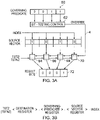
- Figure 3A schematically illustrates the relevant components of the data processing circuitry in a further example embodiment, wherein here the bit-testing procedure is carried out in further dependence on the content of a set of governing predicate bit values.
- a corresponding pair of bit-testing instructions, also called TSTZ and TSTNZ are shown in Figure 3B .
- the respective bits of the set of governing predicate bit values, shown as item 60 in Figure 3A determine whether a particular element of the source vector is subjected to the bit-testing of the bit-testing procedure or not. In the example shown, only the elements of the source vector for which the corresponding bit of the set of governing predicate bit values is set to 1 are subjected to this bit-testing.
- bit-testing control circuitry 62 receives the set of governing predicate bit values 60 and generates a set of override signals which control the operation of the bit-testing comparators 64, 66, 68, and 70. As in the example of Figure 2 , these comparators receive the corresponding bit to be tested identified by the index value from the respected element of the source vector and are also controlled by the binary TSTZ / TSTNZ input. A set of result bits 72 is thus generated by the comparators.
- the TSTZ and TSTNZ instructions in this example specify a source vector register and an immediate index value as in the example of Figure 2 , but here further specify a governing predicate register and a destination register. Accordingly the set of governing predicate bit values 60 is retrieved from the specified governing predicate register, whilst the set of result bits 72 is written into the specified destination register. It will be appreciated that there is no significance to the fact that the instruction of Figure 3B additionally specifies both the destination register and the governing predicate register with respect to the example of Figure 2 , and in other example embodiments the bit-testing instruction might specify only one of these in addition to the source register and the index.
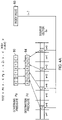
- Figure 4A shows an example in which a TSTZ instruction specifies a destination register, a governing predicate register, a source vector register, an index (scalar) register.
- FIG. 4A For simplicity of illustration an abbreviated configuration is shown in Figure 4A wherein an arrow leads directly from the tested bits of the source vector Zs to the respective result bit of the destination predicate 84.
- these arrows are implemented via a set of comparators such as those shown in the example of Figure 3A , wherein these are controlled by a respective bit of the governing predicate 80 and also by a binary value indicating whether the instruction is TSTZ or TSTNZ.
- the tested bits are inverted to provide the corresponding bits of the destination predicate 84 (this being illustrated in Figure 4A by the notation: source bit (0/1) goes to result bit (1/0)).
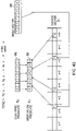
- FIG. 4B an example of a TSTNZ instruction is given which also specifies a destination result register, a governing predicate register and a source vector register, and in this example specifies an index vector register.
- the governing predicate 86 again selects the elements of the source vector Zs which are to be subjected to the bit-testing procedure, which bit is tested in each tested element is individually specified by the index given in the corresponding element of the index vector 88.
- bit position 4 is tested in element 0
- bit position 2 is tested in element 2
- bit position 7 is tested in element 4
- bit position 0 is tested in element 6.
- No bit is tested in elements 1, 3, 5, and 7 since the corresponding bits in the governing predicate 86 are set to 0 and accordingly the corresponding bits in the destination of predicate 90 are set to 0.
- FIG. 4B The example given in Figure 4B is that of a TSTNZ instruction and therefore the tested bits of the source vector are effectively copied into the corresponding bits of the destination predicate 90 (this being illustrated in Figure 4B by the notation: source bit (0/1) goes to result bit (0/1)).
- the illustration of Figure 4B is shown for clarity in abbreviated form with an arrow merely leading from the tested bit of the respective element of the source vector Zs to the corresponding bit position of the destination predicate 90.
- these are implemented via a set of comparators which receive the input bit to be tested and are controlled by a binary input indicating whether the instruction is TSTZ or TSTNZ.
- bit-testing instruction may further modify any of its specified registers with a size specifier indicating a size interpretation for the content of that register.
- a size specifier indicating a size interpretation for the content of that register.
- this size specifier ⁇ T> enables the programmer to specify the size of the data value in each element of the respective vector of elements. Accordingly, whilst in the absence of this size specifier, or indeed if the size specifier has value which matches the default, then a default interpretation of the elements of the register may be used, for example "S", single word length. If however, the value of ⁇ T> specified in the instruction, then the specified size of each vector element is used. Further variations on this functionality are also possible for any of the above described example embodiments, in which the size specifier is itself given by a register and the data processing circuitry accesses that specified size specifying register in order to extract the required size value.
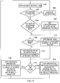
- FIG. 5 shows a sequence of steps which are carried out according to the method of one embodiment.
- the flow can be considered to begin at step 100 at which the instruction decoding circuitry decodes the next instruction in the sequence of instructions provided to the apparatus. For simplicity in this figure it is assumed that there is always another instruction to be decoded.
- step 102 it is determined if this is a bit-testing instruction and if it is not then this instruction is merely executed at step 104 in the usual fashion for this instruction and the flow returns to step 100 (since only the novel bit-testing instructions are of interest here).
- the flow proceeds from step 102 to step 104 where it is determined if any bits of a governing predicate are set to 0.
- step 106 the corresponding bit or bits of the result predicate are also set to 0.
- step 108 it is determined if the bit-testing instruction has specified a vector (as opposed to an immediate or scalar register defined) index. If it has then the flow proceeds via step 110 where a unique index for each processed element of the source vector is used, taken from the corresponding element of the vector index. Otherwise, at step 112 the scalar value of the index (either provided in a scalar register or as an immediate value in the instruction) is used for all processed elements of the source vector. Next at step 144 it is determined whether this is a TSTZ or TSTNZ instruction.
- step 116 the index bit for each processed element of the source vector is copied to the respective bit of the result predicate.
- step 118 the flow proceeds via step 118 at which an inverted index bit for each processed element of the source vector is copied to the respective bit of the result predicate. Execution of this bit-testing instruction is then complete and the flow returns to step 100.
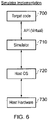
- FIG. 6 illustrates a simulator implementation that may be used. Whilst the earlier described embodiments implement the present invention in terms of apparatus and methods for operating specific processing hardware supporting the techniques concerned, it is also possible to provide an instruction execution environment in accordance with the embodiments described herein which is implemented through the use of a computer program. Such computer programs are often referred to as simulators, insofar as they provide a software based implementation of a hardware architecture. Varieties of simulator computer programs include emulators, virtual machines, models, and binary translators, including dynamic binary translators. Typically, a simulator implementation may run on a host processor 730, optionally running a host operating system 720, supporting the simulator program 710.
- the hardware there may be multiple layers of simulation between the hardware and the provided instruction execution environment, and/or multiple distinct instruction execution environments provided on the same host processor.
- powerful processors have been required to provide simulator implementations which execute at a reasonable speed, but such an approach may be justified in certain circumstances, such as when there is a desire to run code native to another processor for compatibility or re-use reasons.
- the simulator implementation may provide an instruction execution environment with additional functionality which is not supported by the host processor hardware, or provide an instruction execution environment typically associated with a different hardware architecture.
- An overview of simulation is given in " Some Efficient Architecture Simulation Techniques", Robert Bedichek, Winter 1990 USENIX Conference, Pages 53 - 63 .
- a simulated embodiment equivalent functionality may be provided by suitable software constructs or features.
- particular circuitry may be implemented in a simulated embodiment as computer program logic.
- memory hardware such as a register or cache, may be implemented in a simulated embodiment as a software data structure.
- some simulated embodiments may make use of the host hardware, where suitable.
- the simulator program 710 may be stored on a computer-readable storage medium (which may be a non-transitory medium), and provides a program interface (instruction execution environment) to the target code 700 which is the same as the application program interface of the hardware architecture being modelled by the simulator program 710.
- the program instructions of the target code 700 including the bit-testing instructions described above, may be executed from within the instruction execution environment using the simulator program 710, so that a host computer 730 which does not actually have the hardware features of the apparatus discussed above can emulate these features.
- an apparatus and method of operating an apparatus are provided.
- the apparatus is responsive to a bit-testing instruction which specifies a source vector register and an index to perform a bit-testing procedure on plural elements stored in the source vector register to generate plural result bits.
- the bit-testing procedure comprises, for each processed element of the plural elements, setting a respective result bit of the plural result bits in dependence on a value of a tested bit at a bit position in the processed element of the source vector register indicated by the index.
- the words “configured to" are used to mean that an element of an apparatus has a configuration able to carry out the defined operation.
- a “configuration” means an arrangement or manner of interconnection of hardware or software.
- the apparatus may have dedicated hardware which provides the defined operation, or a processor or other processing device may be programmed to perform the function.
- Configured to does not imply that the apparatus element needs to be changed in any way in order to provide the defined operation.
Landscapes
- Engineering & Computer Science (AREA)
- Software Systems (AREA)
- Theoretical Computer Science (AREA)
- Physics & Mathematics (AREA)
- General Engineering & Computer Science (AREA)
- General Physics & Mathematics (AREA)
- Mathematical Physics (AREA)
- Complex Calculations (AREA)
- Executing Machine-Instructions (AREA)
- Test And Diagnosis Of Digital Computers (AREA)
- Advance Control (AREA)
- Compression, Expansion, Code Conversion, And Decoders (AREA)
- Error Detection And Correction (AREA)
- Techniques For Improving Reliability Of Storages (AREA)
- Testing, Inspecting, Measuring Of Stereoscopic Televisions And Televisions (AREA)
Claims (18)
- Appareil, comprenant :une circuiterie de décodage d'instructions pour décoder des instructions et générer des signaux de commande en fonction des instructions ; etune circuiterie de traitement de données pour réaliser des opérations de traitement de données en réaction aux signaux de commande générés par la circuiterie de décodage d'instructions,la circuiterie de décodage d'instructions réagissant à une instruction de test de bit stipulant un registre de vecteur source et un index pour amener la circuiterie de traitement de données à :
réaliser une procédure de test de bit sur une pluralité d'éléments stockés dans le registre de vecteur source pour générer une pluralité de bits de résultat, la procédure de test de bit comprenant, pour chaque élément traité de la pluralité d'éléments :le positionnement d'un bit de résultat respectif de la pluralité de bits de résultat en fonction d'une valeur d'un bit testé à une position de bit dans l'élément traité du registre de vecteur source indiqué par l'index ;dans la procédure de test de bit, un élément de la pluralité d'éléments étant soumis à la procédure de test de bit comme élément traité lorsqu'un bit de prédicat respectif d'un ensemble de valeurs de bit de prédicat prend une première valeur prédéterminée, etdans la procédure de test de bit, chacun de la pluralité de bits de résultat, correspondant à l'une des valeurs de bit de prédicat qui ne prend pas la première valeur prédéterminée, est positionné à une même valeur prédéterminée. - Appareil selon la revendication 1, dans lequel la pluralité d'éléments soumis à la procédure de test de bit comprend tous les éléments du registre de vecteur source.
- Appareil selon la revendication 1, dans lequel un nombre de valeurs dans l'ensemble de valeurs de bit de prédicat concorde avec un nombre d'éléments dans le registre de vecteur source.
- Appareil selon la revendication 3, dans lequel l'instruction de test de bit stipule l'ensemble de valeurs de bit de prédicat.
- Appareil selon la revendication 4, dans lequel l'instruction de test de bit stipule un registre contenant l'ensemble de valeurs de bit de prédicat.
- Appareil selon l'une quelconque des revendications précédentes, dans lequel la circuiterie de traitement de données est agencée pour stocker la pluralité de bits de résultat dans un registre de résultats.
- Appareil selon la revendication 6, dans lequel le registre de résultats est stipulé dans l'instruction de test de bit.
- Appareil selon l'une quelconque des revendications précédentes, dans lequel un compte de la pluralité de bits de résultat concorde avec un compte de la pluralité d'éléments stockés dans le registre de vecteur source.
- Appareil selon l'une quelconque des revendications 1 à 8, dans lequel, dans la procédure de test de bit, le bit de résultat respectif de la pluralité de bits de résultat est positionné de manière à concorder avec la valeur du bit testé.
- Appareil selon l'une quelconque des revendications 1 à 8, dans lequel, dans la procédure de test de bit, le bit de résultat respectif de la pluralité de bits de résultat est positionné de manière à concorder avec la valeur du bit testé.
- Appareil selon la revendication 9, dans lequel la circuiterie de décodage d'instructions réagit à une instruction de test de bit additionnelle, laquelle amène la circuiterie de traitement de données à réaliser une procédure de test de bit additionnelle comprenant le positionnement d'un bit de résultat respectif additionnel d'une pluralité additionnelle de bits de résultat pour qu'il ne concorde pas avec une valeur d'un bit testé additionnel.
- Appareil selon la revendication 10, dans lequel la circuiterie de décodage d'instructions réagit à une instruction de test de bit additionnelle, laquelle amène la circuiterie de traitement de données à réaliser une procédure de test de bit additionnelle comprenant le positionnement d'un bit de résultat respectif additionnel d'une pluralité additionnelle de bits de résultat pour qu'il concorde avec une valeur d'un bit testé additionnel.
- Appareil selon l'une quelconque des revendications 1 à 12, dans lequel l'index est une valeur immédiate dans l'instruction de test de bit.
- Appareil selon l'une quelconque des revendications 1 à 12, dans lequel l'index est une valeur scalaire stockée dans un registre d'index scalaires stipulé dans l'instruction de test de bit.
- Appareil selon l'une quelconque des revendications 1 à 12, dans lequel l'instruction de test de bit stipule un registre d'index de vecteur contenant une pluralité de valeurs d'index et, dans la procédure de test de bit, pour chaque élément traité de la pluralité d'éléments, l'index est donné par une valeur d'index respective de la pluralité de valeurs d'index.
- Procédé pour faire fonctionner un appareil de traitement de données, comprenant :le décodage d'instructions et la génération de signaux de commande en fonction des instructions ;la réalisation d'opérations de traitement de données en réaction aux signaux de commande générés ; eten réaction à une instruction de test de bit stipulant un registre de vecteur source et un index, la commande de la réalisation d'une procédure de test de bit sur une pluralité d'éléments stockés dans le registre de vecteur source pour générer une pluralité de bits de résultat,la procédure de test de bit comprenant, pour chaque élément traité de la pluralité d'éléments :le positionnement d'un bit de résultat respectif de la pluralité de bits de résultat en fonction d'une valeur d'un bit testé à une position de bit dans l'élément traité du registre de vecteur source indiqué par l'index ;dans la procédure de test de bit, un élément de la pluralité d'éléments étant soumis à la procédure de test de bit comme élément traité lorsqu'un bit de prédicat respectif d'un ensemble de valeurs de bit de prédicat prend une première valeur prédéterminée, etdans la procédure de test de bit, chacun de la pluralité de bits de résultat, correspondant à l'une des valeurs de bit de prédicat qui ne prend pas la première valeur prédéterminée, est positionné à une même valeur prédéterminée.
- Programme d'ordinateur comprenant des instructions qui, lorsque le programme est exécuté par un appareil selon la revendication 1, fournissent un environnement d'exécution d'instructions comprenant :une logique de programme de décodage d'instructions pour décoder des instructions et générer des signaux de commande en fonction des instructions ; etune logique de programme de traitement de données pour réaliser des opérations de traitement de données en réaction aux signaux de commande générés par la logique de programme de décodage d'instructions,la logique de programme de décodage d'instructions réagissant à une instruction de test de bit stipulant une structure de données de vecteur source et un index pour amener la logique de programme de traitement de données à :
réaliser une procédure de test de bit sur une pluralité d'éléments stockés dans la structure de données de vecteur source pour générer une pluralité de bits de résultat, la procédure de test de bit comprenant, pour chaque élément traité de la pluralité d'éléments :le positionnement d'un bit de résultat respectif de la pluralité de bits de résultat en fonction d'une valeur d'un bit testé à une position de bit dans l'élément traité de la structure de données de vecteur source indiqué par l'index ;dans la procédure de test de bit, un élément de la pluralité d'éléments étant soumis à la procédure de test de bit comme élément traité lorsqu'un bit de prédicat respectif d'un ensemble de valeurs de bit de prédicat prend une première valeur prédéterminée, etdans la procédure de test de bit, chacun de la pluralité de bits de résultat, correspondant à l'une des valeurs de bit de prédicat qui ne prend pas la première valeur prédéterminée, est positionné à une même valeur prédéterminée. - Support de stockage lisible par ordinateur stockant d'une manière non transitoire le programme d'ordinateur selon la revendication 17.
Priority Applications (9)
| Application Number | Priority Date | Filing Date | Title |
|---|---|---|---|
| EP17386023.0A EP3428792B1 (fr) | 2017-07-10 | 2017-07-10 | Valeurs de bit d'essai à l'intérieur d'éléments vectoriels |
| CN201880044656.XA CN110832455B (zh) | 2017-07-10 | 2018-06-27 | 测试向量元素内部的位值 |
| PCT/EP2018/067234 WO2019011653A1 (fr) | 2017-07-10 | 2018-06-27 | Test de valeurs de bit à l'intérieur d'éléments de vecteur |
| JP2019572555A JP7492830B2 (ja) | 2017-07-10 | 2018-06-27 | ベクトル要素内のビット値のテスト |
| TW107122047A TWI785064B (zh) | 2017-07-10 | 2018-06-27 | 用於測試向量元素內部的位元值的設備、方法、電腦程式及電腦可讀儲存媒體 |
| KR1020207002160A KR102590679B1 (ko) | 2017-07-10 | 2018-06-27 | 벡터 요소들 내부의 비트 값들의 시험 |
| US16/629,178 US11422807B2 (en) | 2017-07-10 | 2018-06-27 | Testing bit values inside vector elements |
| IL271438A IL271438B2 (en) | 2017-07-10 | 2018-06-27 | Checking bit values inside vector elements |
| JP2023040331A JP7557000B2 (ja) | 2017-07-10 | 2023-03-15 | ベクトル要素内のビット値のテスト |
Applications Claiming Priority (1)
| Application Number | Priority Date | Filing Date | Title |
|---|---|---|---|
| EP17386023.0A EP3428792B1 (fr) | 2017-07-10 | 2017-07-10 | Valeurs de bit d'essai à l'intérieur d'éléments vectoriels |
Publications (2)
| Publication Number | Publication Date |
|---|---|
| EP3428792A1 EP3428792A1 (fr) | 2019-01-16 |
| EP3428792B1 true EP3428792B1 (fr) | 2022-05-04 |
Family
ID=59501374
Family Applications (1)
| Application Number | Title | Priority Date | Filing Date |
|---|---|---|---|
| EP17386023.0A Active EP3428792B1 (fr) | 2017-07-10 | 2017-07-10 | Valeurs de bit d'essai à l'intérieur d'éléments vectoriels |
Country Status (8)
| Country | Link |
|---|---|
| US (1) | US11422807B2 (fr) |
| EP (1) | EP3428792B1 (fr) |
| JP (2) | JP7492830B2 (fr) |
| KR (1) | KR102590679B1 (fr) |
| CN (1) | CN110832455B (fr) |
| IL (1) | IL271438B2 (fr) |
| TW (1) | TWI785064B (fr) |
| WO (1) | WO2019011653A1 (fr) |
Families Citing this family (6)
| Publication number | Priority date | Publication date | Assignee | Title |
|---|---|---|---|---|
| US11593105B2 (en) * | 2018-12-29 | 2023-02-28 | Intel Corporation | Vector logical operation and test instructions with result negation |
| US11403256B2 (en) | 2019-05-20 | 2022-08-02 | Micron Technology, Inc. | Conditional operations in a vector processor having true and false vector index registers |
| US11340904B2 (en) | 2019-05-20 | 2022-05-24 | Micron Technology, Inc. | Vector index registers |
| US11507374B2 (en) * | 2019-05-20 | 2022-11-22 | Micron Technology, Inc. | True/false vector index registers and methods of populating thereof |
| US11327862B2 (en) | 2019-05-20 | 2022-05-10 | Micron Technology, Inc. | Multi-lane solutions for addressing vector elements using vector index registers |
| CN116973736B (zh) * | 2023-09-22 | 2023-12-19 | 悦芯科技股份有限公司 | 一种基于fail周期的ATE测试方法及系统 |
Family Cites Families (37)
| Publication number | Priority date | Publication date | Assignee | Title |
|---|---|---|---|---|
| JPS5353237A (en) * | 1976-10-26 | 1978-05-15 | Toshiba Corp | Program switching device |
| US6414368B1 (en) * | 1982-11-26 | 2002-07-02 | Stmicroelectronics Limited | Microcomputer with high density RAM on single chip |
| JPH02230320A (ja) * | 1989-03-03 | 1990-09-12 | Hitachi Ltd | データ処理装置 |
| JPH05108542A (ja) * | 1991-10-16 | 1993-04-30 | Hitachi Ltd | データ処理装置 |
| US5473531A (en) * | 1993-12-28 | 1995-12-05 | At&T Corp. | Finite state machine with minimized memory requirements |
| US5459841A (en) * | 1993-12-28 | 1995-10-17 | At&T Corp. | Finite state machine with minimized vector processing |
| US5623680A (en) * | 1993-12-28 | 1997-04-22 | Lucent Technologies Inc. | Finite state machine for process control |
| DE69838028T2 (de) * | 1998-10-06 | 2008-03-13 | Texas Instruments Inc., Dallas | Linearvektorrechnung |
| US7124160B2 (en) * | 2000-03-08 | 2006-10-17 | Sun Microsystems, Inc. | Processing architecture having parallel arithmetic capability |
| JP4626032B2 (ja) * | 2000-08-28 | 2011-02-02 | 株式会社デンソー | プログラム変換装置,プログラム変換方法及び記録媒体 |
| US20020188830A1 (en) * | 2001-06-01 | 2002-12-12 | Brian Boles | Bit replacement and extraction instructions |
| GB2382673B (en) * | 2001-10-31 | 2005-10-26 | Alphamosaic Ltd | A vector processing system |
| US7043511B1 (en) * | 2002-08-30 | 2006-05-09 | Lattice Semiconductor Corporation | Performing conditional operations in a programmable logic device |
| US7548944B2 (en) * | 2003-07-15 | 2009-06-16 | Intel Corporation | Statistics collection framework for a network processor |
| GB2409063B (en) | 2003-12-09 | 2006-07-12 | Advanced Risc Mach Ltd | Vector by scalar operations |
| US9557994B2 (en) * | 2004-07-13 | 2017-01-31 | Arm Limited | Data processing apparatus and method for performing N-way interleaving and de-interleaving operations where N is an odd plural number |
| US8457419B2 (en) * | 2007-04-13 | 2013-06-04 | Research In Motion Limited | Method of decoding entropy-encoded data |
| US20090254694A1 (en) * | 2008-04-02 | 2009-10-08 | Zikbit Ltd. | Memory device with integrated parallel processing |
| US8433883B2 (en) * | 2009-06-11 | 2013-04-30 | Cray Inc. | Inclusive “OR” bit matrix compare resolution of vector update conflict masks |
| EP2584460A1 (fr) * | 2011-10-20 | 2013-04-24 | ST-Ericsson SA | Système de traitement de vecteurs avec un sous-système de réplication et procédé |
| US9792117B2 (en) * | 2011-12-08 | 2017-10-17 | Oracle International Corporation | Loading values from a value vector into subregisters of a single instruction multiple data register |
| WO2013095606A1 (fr) * | 2011-12-23 | 2013-06-27 | Intel Corporation | Appareil et procédé permettant de détecter des éléments identiques à l'intérieur d'un registre vectoriel |
| US10055225B2 (en) * | 2011-12-23 | 2018-08-21 | Intel Corporation | Multi-register scatter instruction |
| EP2798504A4 (fr) * | 2011-12-29 | 2016-07-27 | Intel Corp | Processeurs ayant des interconnexions entièrement connectées partagées par des instructions de conflit vectoriel et des instructions de permutation |
| US9715383B2 (en) * | 2012-03-15 | 2017-07-25 | International Business Machines Corporation | Vector find element equal instruction |
| US9588762B2 (en) * | 2012-03-15 | 2017-03-07 | International Business Machines Corporation | Vector find element not equal instruction |
| US9424031B2 (en) * | 2013-03-13 | 2016-08-23 | Intel Corporation | Techniques for enabling bit-parallel wide string matching with a SIMD register |
| US9411593B2 (en) * | 2013-03-15 | 2016-08-09 | Intel Corporation | Processors, methods, systems, and instructions to consolidate unmasked elements of operation masks |
| US20150186137A1 (en) * | 2013-12-27 | 2015-07-02 | Tal Uliel | Systems, apparatuses, and methods for vector bit test |
| US9830151B2 (en) * | 2014-12-23 | 2017-11-28 | Intel Corporation | Method and apparatus for vector index load and store |
| US20160179520A1 (en) * | 2014-12-23 | 2016-06-23 | Intel Corporation | Method and apparatus for variably expanding between mask and vector registers |
| US10445092B2 (en) * | 2014-12-27 | 2019-10-15 | Intel Corporation | Method and apparatus for performing a vector permute with an index and an immediate |
| US10001995B2 (en) | 2015-06-02 | 2018-06-19 | Intel Corporation | Packed data alignment plus compute instructions, processors, methods, and systems |
| GB2540943B (en) * | 2015-07-31 | 2018-04-11 | Advanced Risc Mach Ltd | Vector arithmetic instruction |
| US10198264B2 (en) * | 2015-12-15 | 2019-02-05 | Intel Corporation | Sorting data and merging sorted data in an instruction set architecture |
| WO2018022528A1 (fr) * | 2016-07-27 | 2018-02-01 | Intel Corporation | Système et procédé de multiplexage de comparaison de vecteurs |
| US10747819B2 (en) * | 2018-04-20 | 2020-08-18 | International Business Machines Corporation | Rapid partial substring matching |
-
2017
- 2017-07-10 EP EP17386023.0A patent/EP3428792B1/fr active Active
-
2018
- 2018-06-27 JP JP2019572555A patent/JP7492830B2/ja active Active
- 2018-06-27 WO PCT/EP2018/067234 patent/WO2019011653A1/fr active Application Filing
- 2018-06-27 IL IL271438A patent/IL271438B2/en unknown
- 2018-06-27 US US16/629,178 patent/US11422807B2/en active Active
- 2018-06-27 CN CN201880044656.XA patent/CN110832455B/zh active Active
- 2018-06-27 TW TW107122047A patent/TWI785064B/zh active
- 2018-06-27 KR KR1020207002160A patent/KR102590679B1/ko active IP Right Grant
-
2023
- 2023-03-15 JP JP2023040331A patent/JP7557000B2/ja active Active
Also Published As
| Publication number | Publication date |
|---|---|
| IL271438B1 (en) | 2023-10-01 |
| JP7557000B2 (ja) | 2024-09-26 |
| EP3428792A1 (fr) | 2019-01-16 |
| CN110832455B (zh) | 2023-09-29 |
| TW201908757A (zh) | 2019-03-01 |
| US20200225953A1 (en) | 2020-07-16 |
| IL271438A (en) | 2020-01-30 |
| KR102590679B1 (ko) | 2023-10-18 |
| IL271438B2 (en) | 2024-02-01 |
| CN110832455A (zh) | 2020-02-21 |
| TWI785064B (zh) | 2022-12-01 |
| JP2023085319A (ja) | 2023-06-20 |
| US11422807B2 (en) | 2022-08-23 |
| WO2019011653A1 (fr) | 2019-01-17 |
| JP7492830B2 (ja) | 2024-05-30 |
| JP2020526825A (ja) | 2020-08-31 |
| KR20200021517A (ko) | 2020-02-28 |
Similar Documents
| Publication | Publication Date | Title |
|---|---|---|
| EP3428792B1 (fr) | Valeurs de bit d'essai à l'intérieur d'éléments vectoriels | |
| JP4653236B2 (ja) | ユーザ選択可能なストレージ・アクセス・キーを用いてデータを移動する方法及びシステム | |
| US10409602B2 (en) | Vector operand bitsize control | |
| EP3662361B1 (fr) | Mise en correspondance de valeurs consécutives dans un appareil de traitement de données | |
| JP7335952B2 (ja) | ベクトル述語要約の生成 | |
| WO2022074355A1 (fr) | Instruction de comparaison de vecteurs masqués | |
| US11354126B2 (en) | Data processing | |
| US20240329996A1 (en) | Predication techniques | |
| US11099848B1 (en) | Overlapped-immediate/register-field-specifying instruction | |
| EP4244712A1 (fr) | Filtrage basé sur un spécificateur de plage | |
| CN111527480A (zh) | 数据处理装置中的地址转换 |
Legal Events
| Date | Code | Title | Description |
|---|---|---|---|
| PUAI | Public reference made under article 153(3) epc to a published international application that has entered the european phase |
Free format text: ORIGINAL CODE: 0009012 |
|
| STAA | Information on the status of an ep patent application or granted ep patent |
Free format text: STATUS: THE APPLICATION HAS BEEN PUBLISHED |
|
| AK | Designated contracting states |
Kind code of ref document: A1 Designated state(s): AL AT BE BG CH CY CZ DE DK EE ES FI FR GB GR HR HU IE IS IT LI LT LU LV MC MK MT NL NO PL PT RO RS SE SI SK SM TR |
|
| AX | Request for extension of the european patent |
Extension state: BA ME |
|
| STAA | Information on the status of an ep patent application or granted ep patent |
Free format text: STATUS: REQUEST FOR EXAMINATION WAS MADE |
|
| 17P | Request for examination filed |
Effective date: 20190710 |
|
| RBV | Designated contracting states (corrected) |
Designated state(s): AL AT BE BG CH CY CZ DE DK EE ES FI FR GB GR HR HU IE IS IT LI LT LU LV MC MK MT NL NO PL PT RO RS SE SI SK SM TR |
|
| STAA | Information on the status of an ep patent application or granted ep patent |
Free format text: STATUS: EXAMINATION IS IN PROGRESS |
|
| 17Q | First examination report despatched |
Effective date: 20200207 |
|
| STAA | Information on the status of an ep patent application or granted ep patent |
Free format text: STATUS: EXAMINATION IS IN PROGRESS |
|
| GRAP | Despatch of communication of intention to grant a patent |
Free format text: ORIGINAL CODE: EPIDOSNIGR1 |
|
| STAA | Information on the status of an ep patent application or granted ep patent |
Free format text: STATUS: GRANT OF PATENT IS INTENDED |
|
| INTG | Intention to grant announced |
Effective date: 20211209 |
|
| GRAS | Grant fee paid |
Free format text: ORIGINAL CODE: EPIDOSNIGR3 |
|
| GRAA | (expected) grant |
Free format text: ORIGINAL CODE: 0009210 |
|
| STAA | Information on the status of an ep patent application or granted ep patent |
Free format text: STATUS: THE PATENT HAS BEEN GRANTED |
|
| AK | Designated contracting states |
Kind code of ref document: B1 Designated state(s): AL AT BE BG CH CY CZ DE DK EE ES FI FR GB GR HR HU IE IS IT LI LT LU LV MC MK MT NL NO PL PT RO RS SE SI SK SM TR |
|
| REG | Reference to a national code |
Ref country code: GB Ref legal event code: FG4D |
|
| REG | Reference to a national code |
Ref country code: CH Ref legal event code: EP |
|
| REG | Reference to a national code |
Ref country code: AT Ref legal event code: REF Ref document number: 1489804 Country of ref document: AT Kind code of ref document: T Effective date: 20220515 |
|
| REG | Reference to a national code |
Ref country code: IE Ref legal event code: FG4D Ref country code: DE Ref legal event code: R096 Ref document number: 602017056848 Country of ref document: DE |
|
| REG | Reference to a national code |
Ref country code: LT Ref legal event code: MG9D |
|
| REG | Reference to a national code |
Ref country code: NL Ref legal event code: MP Effective date: 20220504 |
|
| REG | Reference to a national code |
Ref country code: AT Ref legal event code: MK05 Ref document number: 1489804 Country of ref document: AT Kind code of ref document: T Effective date: 20220504 |
|
| PG25 | Lapsed in a contracting state [announced via postgrant information from national office to epo] |
Ref country code: SE Free format text: LAPSE BECAUSE OF FAILURE TO SUBMIT A TRANSLATION OF THE DESCRIPTION OR TO PAY THE FEE WITHIN THE PRESCRIBED TIME-LIMIT Effective date: 20220504 Ref country code: PT Free format text: LAPSE BECAUSE OF FAILURE TO SUBMIT A TRANSLATION OF THE DESCRIPTION OR TO PAY THE FEE WITHIN THE PRESCRIBED TIME-LIMIT Effective date: 20220905 Ref country code: NO Free format text: LAPSE BECAUSE OF FAILURE TO SUBMIT A TRANSLATION OF THE DESCRIPTION OR TO PAY THE FEE WITHIN THE PRESCRIBED TIME-LIMIT Effective date: 20220804 Ref country code: NL Free format text: LAPSE BECAUSE OF FAILURE TO SUBMIT A TRANSLATION OF THE DESCRIPTION OR TO PAY THE FEE WITHIN THE PRESCRIBED TIME-LIMIT Effective date: 20220504 Ref country code: LT Free format text: LAPSE BECAUSE OF FAILURE TO SUBMIT A TRANSLATION OF THE DESCRIPTION OR TO PAY THE FEE WITHIN THE PRESCRIBED TIME-LIMIT Effective date: 20220504 Ref country code: HR Free format text: LAPSE BECAUSE OF FAILURE TO SUBMIT A TRANSLATION OF THE DESCRIPTION OR TO PAY THE FEE WITHIN THE PRESCRIBED TIME-LIMIT Effective date: 20220504 Ref country code: GR Free format text: LAPSE BECAUSE OF FAILURE TO SUBMIT A TRANSLATION OF THE DESCRIPTION OR TO PAY THE FEE WITHIN THE PRESCRIBED TIME-LIMIT Effective date: 20220805 Ref country code: FI Free format text: LAPSE BECAUSE OF FAILURE TO SUBMIT A TRANSLATION OF THE DESCRIPTION OR TO PAY THE FEE WITHIN THE PRESCRIBED TIME-LIMIT Effective date: 20220504 Ref country code: ES Free format text: LAPSE BECAUSE OF FAILURE TO SUBMIT A TRANSLATION OF THE DESCRIPTION OR TO PAY THE FEE WITHIN THE PRESCRIBED TIME-LIMIT Effective date: 20220504 Ref country code: BG Free format text: LAPSE BECAUSE OF FAILURE TO SUBMIT A TRANSLATION OF THE DESCRIPTION OR TO PAY THE FEE WITHIN THE PRESCRIBED TIME-LIMIT Effective date: 20220804 Ref country code: AT Free format text: LAPSE BECAUSE OF FAILURE TO SUBMIT A TRANSLATION OF THE DESCRIPTION OR TO PAY THE FEE WITHIN THE PRESCRIBED TIME-LIMIT Effective date: 20220504 |
|
| PG25 | Lapsed in a contracting state [announced via postgrant information from national office to epo] |
Ref country code: RS Free format text: LAPSE BECAUSE OF FAILURE TO SUBMIT A TRANSLATION OF THE DESCRIPTION OR TO PAY THE FEE WITHIN THE PRESCRIBED TIME-LIMIT Effective date: 20220504 Ref country code: PL Free format text: LAPSE BECAUSE OF FAILURE TO SUBMIT A TRANSLATION OF THE DESCRIPTION OR TO PAY THE FEE WITHIN THE PRESCRIBED TIME-LIMIT Effective date: 20220504 Ref country code: LV Free format text: LAPSE BECAUSE OF FAILURE TO SUBMIT A TRANSLATION OF THE DESCRIPTION OR TO PAY THE FEE WITHIN THE PRESCRIBED TIME-LIMIT Effective date: 20220504 Ref country code: IS Free format text: LAPSE BECAUSE OF FAILURE TO SUBMIT A TRANSLATION OF THE DESCRIPTION OR TO PAY THE FEE WITHIN THE PRESCRIBED TIME-LIMIT Effective date: 20220904 |
|
| PG25 | Lapsed in a contracting state [announced via postgrant information from national office to epo] |
Ref country code: SM Free format text: LAPSE BECAUSE OF FAILURE TO SUBMIT A TRANSLATION OF THE DESCRIPTION OR TO PAY THE FEE WITHIN THE PRESCRIBED TIME-LIMIT Effective date: 20220504 Ref country code: SK Free format text: LAPSE BECAUSE OF FAILURE TO SUBMIT A TRANSLATION OF THE DESCRIPTION OR TO PAY THE FEE WITHIN THE PRESCRIBED TIME-LIMIT Effective date: 20220504 Ref country code: RO Free format text: LAPSE BECAUSE OF FAILURE TO SUBMIT A TRANSLATION OF THE DESCRIPTION OR TO PAY THE FEE WITHIN THE PRESCRIBED TIME-LIMIT Effective date: 20220504 Ref country code: EE Free format text: LAPSE BECAUSE OF FAILURE TO SUBMIT A TRANSLATION OF THE DESCRIPTION OR TO PAY THE FEE WITHIN THE PRESCRIBED TIME-LIMIT Effective date: 20220504 Ref country code: DK Free format text: LAPSE BECAUSE OF FAILURE TO SUBMIT A TRANSLATION OF THE DESCRIPTION OR TO PAY THE FEE WITHIN THE PRESCRIBED TIME-LIMIT Effective date: 20220504 Ref country code: CZ Free format text: LAPSE BECAUSE OF FAILURE TO SUBMIT A TRANSLATION OF THE DESCRIPTION OR TO PAY THE FEE WITHIN THE PRESCRIBED TIME-LIMIT Effective date: 20220504 |
|
| REG | Reference to a national code |
Ref country code: DE Ref legal event code: R097 Ref document number: 602017056848 Country of ref document: DE |
|
| PG25 | Lapsed in a contracting state [announced via postgrant information from national office to epo] |
Ref country code: MC Free format text: LAPSE BECAUSE OF FAILURE TO SUBMIT A TRANSLATION OF THE DESCRIPTION OR TO PAY THE FEE WITHIN THE PRESCRIBED TIME-LIMIT Effective date: 20220504 |
|
| REG | Reference to a national code |
Ref country code: CH Ref legal event code: PL |
|
| PLBE | No opposition filed within time limit |
Free format text: ORIGINAL CODE: 0009261 |
|
| STAA | Information on the status of an ep patent application or granted ep patent |
Free format text: STATUS: NO OPPOSITION FILED WITHIN TIME LIMIT |
|
| REG | Reference to a national code |
Ref country code: BE Ref legal event code: MM Effective date: 20220731 |
|
| PG25 | Lapsed in a contracting state [announced via postgrant information from national office to epo] |
Ref country code: AL Free format text: LAPSE BECAUSE OF FAILURE TO SUBMIT A TRANSLATION OF THE DESCRIPTION OR TO PAY THE FEE WITHIN THE PRESCRIBED TIME-LIMIT Effective date: 20220504 |
|
| 26N | No opposition filed |
Effective date: 20230207 |
|
| PG25 | Lapsed in a contracting state [announced via postgrant information from national office to epo] |
Ref country code: LU Free format text: LAPSE BECAUSE OF NON-PAYMENT OF DUE FEES Effective date: 20220710 Ref country code: LI Free format text: LAPSE BECAUSE OF NON-PAYMENT OF DUE FEES Effective date: 20220731 Ref country code: CH Free format text: LAPSE BECAUSE OF NON-PAYMENT OF DUE FEES Effective date: 20220731 |
|
| PG25 | Lapsed in a contracting state [announced via postgrant information from national office to epo] |
Ref country code: SI Free format text: LAPSE BECAUSE OF FAILURE TO SUBMIT A TRANSLATION OF THE DESCRIPTION OR TO PAY THE FEE WITHIN THE PRESCRIBED TIME-LIMIT Effective date: 20220504 Ref country code: BE Free format text: LAPSE BECAUSE OF NON-PAYMENT OF DUE FEES Effective date: 20220731 |
|
| P01 | Opt-out of the competence of the unified patent court (upc) registered |
Effective date: 20230429 |
|
| PG25 | Lapsed in a contracting state [announced via postgrant information from national office to epo] |
Ref country code: IE Free format text: LAPSE BECAUSE OF NON-PAYMENT OF DUE FEES Effective date: 20220710 |
|
| PG25 | Lapsed in a contracting state [announced via postgrant information from national office to epo] |
Ref country code: IT Free format text: LAPSE BECAUSE OF FAILURE TO SUBMIT A TRANSLATION OF THE DESCRIPTION OR TO PAY THE FEE WITHIN THE PRESCRIBED TIME-LIMIT Effective date: 20220504 |
|
| PG25 | Lapsed in a contracting state [announced via postgrant information from national office to epo] |
Ref country code: HU Free format text: LAPSE BECAUSE OF FAILURE TO SUBMIT A TRANSLATION OF THE DESCRIPTION OR TO PAY THE FEE WITHIN THE PRESCRIBED TIME-LIMIT; INVALID AB INITIO Effective date: 20170710 |
|
| PG25 | Lapsed in a contracting state [announced via postgrant information from national office to epo] |
Ref country code: MK Free format text: LAPSE BECAUSE OF FAILURE TO SUBMIT A TRANSLATION OF THE DESCRIPTION OR TO PAY THE FEE WITHIN THE PRESCRIBED TIME-LIMIT Effective date: 20220504 Ref country code: CY Free format text: LAPSE BECAUSE OF FAILURE TO SUBMIT A TRANSLATION OF THE DESCRIPTION OR TO PAY THE FEE WITHIN THE PRESCRIBED TIME-LIMIT Effective date: 20220504 |
|
| PGFP | Annual fee paid to national office [announced via postgrant information from national office to epo] |
Ref country code: GB Payment date: 20240620 Year of fee payment: 8 |
|
| PGFP | Annual fee paid to national office [announced via postgrant information from national office to epo] |
Ref country code: FR Payment date: 20240619 Year of fee payment: 8 |
|
| PG25 | Lapsed in a contracting state [announced via postgrant information from national office to epo] |
Ref country code: MT Free format text: LAPSE BECAUSE OF FAILURE TO SUBMIT A TRANSLATION OF THE DESCRIPTION OR TO PAY THE FEE WITHIN THE PRESCRIBED TIME-LIMIT Effective date: 20220504 |
|
| PGFP | Annual fee paid to national office [announced via postgrant information from national office to epo] |
Ref country code: DE Payment date: 20240619 Year of fee payment: 8 |