EP3425676A1 - Mosfet device of silicon carbide having an integrated diode and manufacturing process thereof - Google Patents
Mosfet device of silicon carbide having an integrated diode and manufacturing process thereof Download PDFInfo
- Publication number
- EP3425676A1 EP3425676A1 EP18181848.5A EP18181848A EP3425676A1 EP 3425676 A1 EP3425676 A1 EP 3425676A1 EP 18181848 A EP18181848 A EP 18181848A EP 3425676 A1 EP3425676 A1 EP 3425676A1
- Authority
- EP
- European Patent Office
- Prior art keywords
- region
- regions
- isolated gate
- implanted
- forming
- Prior art date
- Legal status (The legal status is an assumption and is not a legal conclusion. Google has not performed a legal analysis and makes no representation as to the accuracy of the status listed.)
- Granted
Links
Images





Classifications
-
- H—ELECTRICITY
- H10—SEMICONDUCTOR DEVICES; ELECTRIC SOLID-STATE DEVICES NOT OTHERWISE PROVIDED FOR
- H10D—INORGANIC ELECTRIC SEMICONDUCTOR DEVICES
- H10D8/00—Diodes
- H10D8/60—Schottky-barrier diodes
-
- H—ELECTRICITY
- H10—SEMICONDUCTOR DEVICES; ELECTRIC SOLID-STATE DEVICES NOT OTHERWISE PROVIDED FOR
- H10D—INORGANIC ELECTRIC SEMICONDUCTOR DEVICES
- H10D84/00—Integrated devices formed in or on semiconductor substrates that comprise only semiconducting layers, e.g. on Si wafers or on GaAs-on-Si wafers
- H10D84/80—Integrated devices formed in or on semiconductor substrates that comprise only semiconducting layers, e.g. on Si wafers or on GaAs-on-Si wafers characterised by the integration of at least one component covered by groups H10D12/00 or H10D30/00, e.g. integration of IGFETs
- H10D84/811—Combinations of field-effect devices and one or more diodes, capacitors or resistors
-
- H—ELECTRICITY
- H10—SEMICONDUCTOR DEVICES; ELECTRIC SOLID-STATE DEVICES NOT OTHERWISE PROVIDED FOR
- H10D—INORGANIC ELECTRIC SEMICONDUCTOR DEVICES
- H10D12/00—Bipolar devices controlled by the field effect, e.g. insulated-gate bipolar transistors [IGBT]
- H10D12/01—Manufacture or treatment
- H10D12/031—Manufacture or treatment of IGBTs
-
- H—ELECTRICITY
- H10—SEMICONDUCTOR DEVICES; ELECTRIC SOLID-STATE DEVICES NOT OTHERWISE PROVIDED FOR
- H10D—INORGANIC ELECTRIC SEMICONDUCTOR DEVICES
- H10D30/00—Field-effect transistors [FET]
- H10D30/01—Manufacture or treatment
- H10D30/021—Manufacture or treatment of FETs having insulated gates [IGFET]
- H10D30/028—Manufacture or treatment of FETs having insulated gates [IGFET] of double-diffused metal oxide semiconductor [DMOS] FETs
- H10D30/0291—Manufacture or treatment of FETs having insulated gates [IGFET] of double-diffused metal oxide semiconductor [DMOS] FETs of vertical DMOS [VDMOS] FETs
-
- H—ELECTRICITY
- H10—SEMICONDUCTOR DEVICES; ELECTRIC SOLID-STATE DEVICES NOT OTHERWISE PROVIDED FOR
- H10D—INORGANIC ELECTRIC SEMICONDUCTOR DEVICES
- H10D30/00—Field-effect transistors [FET]
- H10D30/60—Insulated-gate field-effect transistors [IGFET]
- H10D30/63—Vertical IGFETs
-
- H—ELECTRICITY
- H10—SEMICONDUCTOR DEVICES; ELECTRIC SOLID-STATE DEVICES NOT OTHERWISE PROVIDED FOR
- H10D—INORGANIC ELECTRIC SEMICONDUCTOR DEVICES
- H10D62/00—Semiconductor bodies, or regions thereof, of devices having potential barriers
- H10D62/10—Shapes, relative sizes or dispositions of the regions of the semiconductor bodies; Shapes of the semiconductor bodies
- H10D62/102—Constructional design considerations for preventing surface leakage or controlling electric field concentration
- H10D62/103—Constructional design considerations for preventing surface leakage or controlling electric field concentration for increasing or controlling the breakdown voltage of reverse-biased devices
- H10D62/105—Constructional design considerations for preventing surface leakage or controlling electric field concentration for increasing or controlling the breakdown voltage of reverse-biased devices by having particular doping profiles, shapes or arrangements of PN junctions; by having supplementary regions, e.g. junction termination extension [JTE]
- H10D62/106—Constructional design considerations for preventing surface leakage or controlling electric field concentration for increasing or controlling the breakdown voltage of reverse-biased devices by having particular doping profiles, shapes or arrangements of PN junctions; by having supplementary regions, e.g. junction termination extension [JTE] having supplementary regions doped oppositely to or in rectifying contact with regions of the semiconductor bodies, e.g. guard rings with PN or Schottky junctions
-
- H—ELECTRICITY
- H10—SEMICONDUCTOR DEVICES; ELECTRIC SOLID-STATE DEVICES NOT OTHERWISE PROVIDED FOR
- H10D—INORGANIC ELECTRIC SEMICONDUCTOR DEVICES
- H10D62/00—Semiconductor bodies, or regions thereof, of devices having potential barriers
- H10D62/10—Shapes, relative sizes or dispositions of the regions of the semiconductor bodies; Shapes of the semiconductor bodies
- H10D62/124—Shapes, relative sizes or dispositions of the regions of semiconductor bodies or of junctions between the regions
-
- H—ELECTRICITY
- H10—SEMICONDUCTOR DEVICES; ELECTRIC SOLID-STATE DEVICES NOT OTHERWISE PROVIDED FOR
- H10D—INORGANIC ELECTRIC SEMICONDUCTOR DEVICES
- H10D62/00—Semiconductor bodies, or regions thereof, of devices having potential barriers
- H10D62/10—Shapes, relative sizes or dispositions of the regions of the semiconductor bodies; Shapes of the semiconductor bodies
- H10D62/124—Shapes, relative sizes or dispositions of the regions of semiconductor bodies or of junctions between the regions
- H10D62/126—Top-view geometrical layouts of the regions or the junctions
- H10D62/127—Top-view geometrical layouts of the regions or the junctions of cellular field-effect devices, e.g. multicellular DMOS transistors or IGBTs
-
- H—ELECTRICITY
- H10—SEMICONDUCTOR DEVICES; ELECTRIC SOLID-STATE DEVICES NOT OTHERWISE PROVIDED FOR
- H10D—INORGANIC ELECTRIC SEMICONDUCTOR DEVICES
- H10D62/00—Semiconductor bodies, or regions thereof, of devices having potential barriers
- H10D62/10—Shapes, relative sizes or dispositions of the regions of the semiconductor bodies; Shapes of the semiconductor bodies
- H10D62/13—Semiconductor regions connected to electrodes carrying current to be rectified, amplified or switched, e.g. source or drain regions
- H10D62/149—Source or drain regions of field-effect devices
- H10D62/151—Source or drain regions of field-effect devices of IGFETs
-
- H—ELECTRICITY
- H10—SEMICONDUCTOR DEVICES; ELECTRIC SOLID-STATE DEVICES NOT OTHERWISE PROVIDED FOR
- H10D—INORGANIC ELECTRIC SEMICONDUCTOR DEVICES
- H10D62/00—Semiconductor bodies, or regions thereof, of devices having potential barriers
- H10D62/10—Shapes, relative sizes or dispositions of the regions of the semiconductor bodies; Shapes of the semiconductor bodies
- H10D62/17—Semiconductor regions connected to electrodes not carrying current to be rectified, amplified or switched, e.g. channel regions
- H10D62/393—Body regions of DMOS transistors or IGBTs
-
- H—ELECTRICITY
- H10—SEMICONDUCTOR DEVICES; ELECTRIC SOLID-STATE DEVICES NOT OTHERWISE PROVIDED FOR
- H10D—INORGANIC ELECTRIC SEMICONDUCTOR DEVICES
- H10D62/00—Semiconductor bodies, or regions thereof, of devices having potential barriers
- H10D62/80—Semiconductor bodies, or regions thereof, of devices having potential barriers characterised by the materials
- H10D62/83—Semiconductor bodies, or regions thereof, of devices having potential barriers characterised by the materials being Group IV materials, e.g. B-doped Si or undoped Ge
- H10D62/832—Semiconductor bodies, or regions thereof, of devices having potential barriers characterised by the materials being Group IV materials, e.g. B-doped Si or undoped Ge being Group IV materials comprising two or more elements, e.g. SiGe
- H10D62/8325—Silicon carbide
-
- H—ELECTRICITY
- H10—SEMICONDUCTOR DEVICES; ELECTRIC SOLID-STATE DEVICES NOT OTHERWISE PROVIDED FOR
- H10D—INORGANIC ELECTRIC SEMICONDUCTOR DEVICES
- H10D64/00—Electrodes of devices having potential barriers
- H10D64/20—Electrodes characterised by their shapes, relative sizes or dispositions
- H10D64/27—Electrodes not carrying the current to be rectified, amplified, oscillated or switched, e.g. gates
- H10D64/311—Gate electrodes for field-effect devices
- H10D64/411—Gate electrodes for field-effect devices for FETs
- H10D64/511—Gate electrodes for field-effect devices for FETs for IGFETs
- H10D64/517—Gate electrodes for field-effect devices for FETs for IGFETs characterised by the conducting layers
- H10D64/519—Gate electrodes for field-effect devices for FETs for IGFETs characterised by the conducting layers characterised by their top-view geometrical layouts
-
- H—ELECTRICITY
- H10—SEMICONDUCTOR DEVICES; ELECTRIC SOLID-STATE DEVICES NOT OTHERWISE PROVIDED FOR
- H10D—INORGANIC ELECTRIC SEMICONDUCTOR DEVICES
- H10D8/00—Diodes
- H10D8/01—Manufacture or treatment
- H10D8/051—Manufacture or treatment of Schottky diodes
-
- H—ELECTRICITY
- H10—SEMICONDUCTOR DEVICES; ELECTRIC SOLID-STATE DEVICES NOT OTHERWISE PROVIDED FOR
- H10D—INORGANIC ELECTRIC SEMICONDUCTOR DEVICES
- H10D84/00—Integrated devices formed in or on semiconductor substrates that comprise only semiconducting layers, e.g. on Si wafers or on GaAs-on-Si wafers
- H10D84/01—Manufacture or treatment
- H10D84/02—Manufacture or treatment characterised by using material-based technologies
- H10D84/03—Manufacture or treatment characterised by using material-based technologies using Group IV technology, e.g. silicon technology or silicon-carbide [SiC] technology
- H10D84/035—Manufacture or treatment characterised by using material-based technologies using Group IV technology, e.g. silicon technology or silicon-carbide [SiC] technology using silicon carbide [SiC] technology
-
- H—ELECTRICITY
- H10—SEMICONDUCTOR DEVICES; ELECTRIC SOLID-STATE DEVICES NOT OTHERWISE PROVIDED FOR
- H10D—INORGANIC ELECTRIC SEMICONDUCTOR DEVICES
- H10D84/00—Integrated devices formed in or on semiconductor substrates that comprise only semiconducting layers, e.g. on Si wafers or on GaAs-on-Si wafers
- H10D84/101—Integrated devices comprising main components and built-in components, e.g. IGBT having built-in freewheel diode
- H10D84/141—VDMOS having built-in components
- H10D84/146—VDMOS having built-in components the built-in components being Schottky barrier diodes
-
- H—ELECTRICITY
- H10—SEMICONDUCTOR DEVICES; ELECTRIC SOLID-STATE DEVICES NOT OTHERWISE PROVIDED FOR
- H10P—GENERIC PROCESSES OR APPARATUS FOR THE MANUFACTURE OR TREATMENT OF DEVICES COVERED BY CLASS H10
- H10P30/00—Ion implantation into wafers, substrates or parts of devices
- H10P30/20—Ion implantation into wafers, substrates or parts of devices into semiconductor materials, e.g. for doping
- H10P30/202—Ion implantation into wafers, substrates or parts of devices into semiconductor materials, e.g. for doping characterised by the semiconductor materials
- H10P30/204—Ion implantation into wafers, substrates or parts of devices into semiconductor materials, e.g. for doping characterised by the semiconductor materials into Group IV semiconductors
- H10P30/2042—Ion implantation into wafers, substrates or parts of devices into semiconductor materials, e.g. for doping characterised by the semiconductor materials into Group IV semiconductors into crystalline silicon carbide
-
- H—ELECTRICITY
- H10—SEMICONDUCTOR DEVICES; ELECTRIC SOLID-STATE DEVICES NOT OTHERWISE PROVIDED FOR
- H10P—GENERIC PROCESSES OR APPARATUS FOR THE MANUFACTURE OR TREATMENT OF DEVICES COVERED BY CLASS H10
- H10P30/00—Ion implantation into wafers, substrates or parts of devices
- H10P30/20—Ion implantation into wafers, substrates or parts of devices into semiconductor materials, e.g. for doping
- H10P30/21—Ion implantation into wafers, substrates or parts of devices into semiconductor materials, e.g. for doping of electrically active species
Definitions
- the present invention relates to a MOSFET device of silicon carbide having an integrated diode and the manufacturing process thereof.
- vertical-conduction MOSFET Metal Oxide Semiconductor Field-Effect Transistor
- synchronous rectifiers for example in applications with bridge configurations, such as DC/DC converters.
- MOSFET transistors of silicon carbide have recently been proposed, thanks to their ability to reduce power loss and smaller dimensions.
- MOSFET transistor hereinafter, also defined as device 1 of silicon carbide is shown in Figures 1 and 2 .
- the device 1 comprises a body 2, of silicon carbide, with a first conductivity type (for example, of the N type), having an upper surface 2A and a lower surface 2B.
- a first conductivity type for example, of the N type
- the body 2 is formed by a substrate 17 (forming the lower surface 22B) and by an epitaxial layer 16 (forming the upper surface 22A).
- the body 2 accommodates a first and a second body region 3, 5, with a second conductivity type (in the example being considered, of the P type), disposed at a distance from one another and extending in a direction parallel to a first axis Y of a reference frame XYZ; furthermore, the body regions 3, 5 extend from the upper surface 2A into the interior of the body 2 (in a direction parallel to a second axis Z of the reference frame XYZ).
- a second conductivity type in the example being considered, of the P type
- the body regions 3, 5 thus bound in the body 2 an intermediate region 15, facing the upper surface 2A.
- the body regions 3, 5 respectively accommodate a first and a second source region 4, 6, of the N type, extending from the upper surface 2A into the interior of the body regions 3, 5.
- a plurality of enriched regions 7A-7D extend from the first surface 2A of the body 2 into the interior of the source regions 4, 6 down to a greater depth compared with the latter, but nevertheless smaller compared with that of the body regions 3, 5.
- the enriched regions 7A-7D comprise first enriched regions 7A and 7C ( Figure 2 ) extending through the first source region 4 and mutually aligned in a direction parallel to a third axis X of the reference frame XYZ.
- the enriched regions 7A-7D comprise second enriched regions 7B and 7D, extending through the second source region 6 and mutually aligned in a direction parallel to the third axis X (as can in particular be seen in Figure 2 ).
- an insulating region 8 for example of silicon oxide (SiO 2 ), extends over the upper surface 2A.
- the insulating region 8 extends on top of the intermediate region 15 and, partially, on top of one end of both the body regions 3, 5 and of one end of both the source regions 4, 6.
- the insulating region 8, the conductive region 9 and the layer of dielectric 10 form an isolated gate region 12; the conductive region 9 is furthermore electrically coupled to a gate terminal G of the device 1.
- an upper metallization layer 13 (shown with dashed lines) extends over the entire upper surface 2A and a lower metallization layer 11 extends over the entire lower surface 2B, in such a manner as to guarantee the electrical connection and the operation of the device 1.
- the upper metallization layer 13 forms, in contact with the source regions 4, 6, a source terminal S of the device 1.
- the lower metallization layer 11 forms, in contact with the body 2, a drain terminal D of the device 1.
- body-drain diode The junction between the body 2 and the lower metallization layer 11 forms, inside of the device 1, a diode known as "body-drain diode" which can operate alternately to the device 1 in a conduction phase, as desired in some applications, for example when the device 1 is used in a bridge configuration.
- the body-drain diode in the device 1 has high switching times, a high voltage drop (greater than 2 V) and can emit electromagnetic radiation, reducing the performance of the device 1.
- one solution proposed is to form a diode, for example of the Schottky or JBS (Junction-Barrier Schottky) type, in parallel with the MOSFET transistor and in the same package; indeed, by means of the parallel structure, it is possible to improve the performance characteristics of the MOSFET transistor in applications with a bridge configuration.
- a diode for example of the Schottky or JBS (Junction-Barrier Schottky) type
- the patent EP 1 432 037 A2 describes a MOSFET device, wherein a Schottky diode is integrated with a MOS transistor in one and the same body of silicon.
- a Schottky diode is integrated with a MOS transistor in one and the same body of silicon.
- the solution described in this patent, and in particular the process flow presented in it cannot be immediately applied to silicon carbide devices, in that the temperatures of activation of the silicon carbide are very high (higher than 1600°C) and can damage the conductive region of polysilicon belonging to the isolated gate region 12.
- a silicon carbide MOSFET device is proposed with a structure similar to that presented in the patent EP 1 432 037 A2 ; in the case of US 2013/0313570 A1 , in the MOSFET transistor, a contact of the Schottky type is formed in the body region in contact with a first metallization layer and an ohmic contact in the source region in contact with a second metallization layer.
- the two metallization layers are formed using different metals.
- this solution does not allow the dimensions of the elementary cells of the MOSFET device to be reduced, since it teaches the formation of Schottky contacts inside of these elementary cells.
- the aim of the present invention is to realize a MOSFET device that overcomes the drawbacks of the prior art.
- an integrated MOSFET device is realized and a manufacturing process thereof is carried out, as defined in the appended claims.
- Figures 3-5 show a device 20 including a MOSFET transistor 54 and a JBS (Junction-Barrier Schottky) diode 53, in parallel with the MOSFET transistor 54 (see, in particular, the electrical equivalent in Figure 5 ).
- JBS Joint-Barrier Schottky
- the device 20 is formed here in a body 22, of silicon carbide, with a first conductivity type (for example, of the N type), having an upper surface 22A and a lower surface 22B.
- a first conductivity type for example, of the N type
- the body 22 is formed by a substrate 47 (defining the lower surface 22B) and by an epitaxial layer 46 (defining the upper surface 22A).
- the body 22 accommodates a first and a second body region 23, 25, with a second conductivity type (for example, of the P type) disposed at a distance from one another and extending in a direction parallel to a first axis Y of a reference frame XYZ; furthermore, the body regions 23, 25 extend from the upper surface 22A into the interior of the body 22 (in a direction parallel to a second axis Z of the reference frame XYZ).
- a second conductivity type for example, of the P type
- the body regions 23, 25 thus bound within the body 22 an intermediate region, henceforth referred to as the JFET (Junction Field-Effect Transistor) region 35, facing the upper surface 22A.
- the JFET region 35 accommodates a plurality of implanted regions 40, of the P type, extending into the interior of the body 22 from the upper surface 22A.
- the implanted regions 40 have a width W1, in a direction parallel to a third axis X of the reference frame XYZ, less than the distance between the body regions 23, 25, and a length L in a direction parallel to the first axis Y.
- the width W1 may be in the range between 0.5 ⁇ m and 5 ⁇ m, in particular equal to 1 ⁇ m
- the length L may be in the range between 0.5 and 5 ⁇ m, in particular equal to 1 ⁇ m.
- the implanted regions 40 are mutually aligned in a direction parallel to the first axis Y and bound between them a plurality of intermediate contact portions 37 of the JFET region 35; furthermore, each implanted region 40 is equispaced from the successive one and from the preceding one in a direction parallel to the first axis Y (for example, each implanted region 40 may be separated from the adjacent implanted regions by a distance in the range between 0.5 ⁇ m and 5 ⁇ m, in particular equal to 1 ⁇ m).
- the body regions 23, 25 respectively accommodate a first and a second source region 24, 26, of the N type, extending from the upper surface 22A into the interior of the body regions 23, 25.
- a plurality of enriched regions 27A-27D, of the P type and with a high doping level extends from the first surface 22A of the body 22 into the interior of the source regions 24, 26 over a greater depth compared with the latter, but nevertheless smaller compared with that of the body regions 23, 25.
- the enriched regions 27A-27D comprise first enriched regions 27A and 27C ( Figure 4 ), extending through the first source region 24 and mutually aligned in a direction parallel to the first axis Y, and second enriched regions 27B and 27D, extending through the second source region 26 and mutually aligned in a direction parallel to the first axis Y (as can in particular be seen in Figure 4 ).
- the first enriched regions 27A, 27C are offset by a half-step with respect to the second enriched regions 27B, 27D (as can be seen in Figure 4 ).
- a first and a second insulating region 28, 31, for example of silicon oxide (SiO 2 ) extend, forming gate oxide regions.
- the first insulating region 28 lies partially over the implanted regions 40, extending on top of a first JFET portion 38A and, partially, on top of the first source region 24 and of the first body region 23.
- the second insulating region 31 lies partially over the implanted regions 40, extending on top of a second JFET portion 38B and, partially, on top of the second source region 26 and of the second body region 25.
- the first insulating region 28, the first conductive region 29 and the first dielectric region 30 form a first isolated gate region 36A; the second insulating region 31, the second conductive region 32 and the second dielectric region 33 form a second isolated gate region 36B.
- the first and the second isolated gate regions 36A, 36B form a gate structure 39.
- the first and the second isolated gate region 36A, 36B extend at a distance from one another and are mutually separated by a gap 45 having a width W2, for example, smaller than the width W1 of the implanted regions 40.
- an upper metallization layer 43 (shown in transparency in Figure 3 ) extends over the entire upper surface 22A and a lower metallization layer 44 extends over the entire lower surface 22B, in such a manner as to allow the electrical connection and the operation of the device 20.
- the lower metallization layer 44 in contact with the body 22, forms the drain terminal D of the device 20.
- the upper metallization layer 43 forms a source terminal S of the device 20, in direct contact with the source regions 24, 26; furthermore, the upper metallization layer 43 extends between the isolated gate regions 36A, 36B, within the gap 45, where it is in contact with both the implanted regions 40 in the JFET region 35, here forming an ohmic contact, and with the intermediate contact portions 37, here forming a Schottky contact.
- the device 20 in Figures 3-4 (the electrical equivalent can be seen in Figure 5 ) thus forms a JBS diode 53 in parallel with the MOSFET transistor 54, the latter being formed by the body 22, by the source regions 24, 26 and by the gate structure 39.
- the JBS diode 53 has its cathode terminal coupled to a first conduction node 56 and its anode terminal coupled to a second conduction node 58.
- the first conduction node 56 may be a power supply node and the second conduction node may be coupled to a ground line.
- the conduction nodes 56, 58 may be connected to a first line at a reference potential (for example a power supply line), to a load and/or to a second line at a reference potential (ground line).
- the MOSFET transistor 54 has a gate terminal G designed to receive a control signal s1, a drain terminal D coupled to the first conduction node 56 and a source terminal S coupled to the second conduction node 58. Furthermore, the source terminal S is short-circuited with the body regions 23, 25 of the MOSFET transistor 54.
- the JBS diode 53 is formed by the electrical contact between the upper metallization layer 43, the implanted regions 40 and the intermediate portions 37 in Figures 3 and 4 .
- the control signal s1 is high and commands the MOSFET transistor 54 to turn on; as a result, the MOSFET transistor 54 conducts, allowing a current I to flow from the first conduction node 56 to the second conduction node 58, through the MOSFET transistor 54.
- the JBS diode 53 is nonconducting.
- the control signal s1 is low and the MOSFET transistor 54 is off.
- the JBS diode 53 is conducting and, accordingly, a current I' can flow from the second conduction node 58 to the first conduction node 56 through the JBS diode 53.
- the device 20 may advantageously be used in bridge structures in which it is desired for the MOSFET transistor 54 and the JBS diode 53 to work alternately.
- the device 20 described offers the following advantages. It has a high efficiency by virtue of the presence of the JBS diode 53 in Figure 5 which allows the ignition voltage of the device to be reduced, as shown in Figure 6 , illustrating the voltage-current characteristic in the case of a conventional MOSFET transistor (curve A) and in the case of the device 20 (curve B).
- the described device 20 offers reduced manufacturing costs compared with discrete solutions, wherein a MOSFET transistor and a diode are disposed within separate wafers and reunited in the same package.
- the device 20 in Figures 3 and 4 may be manufactured as shown in Figures 7-11 .
- doping ionic species of the P type for example, aluminium
- the implantation may comprise an implantation sequence at various implantation energies.
- these implantations may take place at a dose in the range between 5 ⁇ 10 13 and 5 ⁇ 10 14 atoms/cm 2 , in particular equal to 1 ⁇ 10 14 atoms/cm 2 with an implantation energy in the range between 20 and 600 keV.
- the JFET region 35 is formed inside the body 22, between the body regions 23, 25, the JFET region 35 is formed.
- an implantation of doping ionic species of the N type, such as nitrogen or phosphorous, is carried out in such a manner as to form the first source region 24 in the first body region 23 and the second source region 26 in the second body region 25.
- this implantation may take place at a dose in the range between 5 ⁇ 10 14 and 1 ⁇ 10 16 atoms/cm 2 , in particular equal to 5 ⁇ 10 15 atoms/cm 2 , with an implantation energy, for example, in the range between 20 keV and 300 keV.
- the implantation of doping ionic species of the P type (for example, aluminium) into the implanted regions 40 and into the enriched regions 27A-27D is carried out by means of known masking and implantation techniques.
- this implantation may take place at a dose in the range between 5 ⁇ 10 14 and 1.10 16 atoms/cm 2 , in particular equal to 5 ⁇ e 15 atoms/cm 2 (with an implantation energy in the range between 20 keV and 300 keV).
- an activation step is carried out, wherein the body 22 is heated to high temperature (for example in the range between 1600°C and 1800°C, in particular to 1700°C) in order to obtain the activation of the doping ionic species and to complete the implantation process.
- the implanted regions 40 and the enriched regions 27A-27D thus formed exhibit a higher doping level compared with body regions 23, 25.
- a gate oxide layer 41 of insulating material, for example silicon oxide, intended to form the insulating regions 28, 31, is deposited over the entire upper surface 22A.
- a gate layer 42 of conductive material, such as polysilicon, intended to form the conductive regions 29, 32, is deposited.
- the gate layer 42 and the oxide layer 41 are defined according to known photolithographic techniques, thus forming the insulating regions 28, 31 and the conductive regions 29, 32.
- the alignment of the masks for the photolithographic definition of the insulating regions 28, 31 and conductive regions 29, 32 with respect to the implanted regions 40 and to the enriched regions 27A-27D takes place by means of common "Zero Layer" techniques, namely taking advantage of the dedicated trenches in non-active regions.
- an insulating layer (not shown) is deposited and defined by means of known deposition and definition techniques, in such a manner as to form the dielectric regions 30, 33.
- the first and the second isolated gate structures 36A, 36B, and therefore the gate structure 39, are thus obtained.
- the lower metallization layer 44 is deposited on the lower surface 22B and the upper metallization layer 43 is deposited on the upper surface 22A, using known deposition and definition techniques.
- the usual final steps thus follow, including the formation of a passivation layer, dicing, etc., obtaining, in such a manner, the device 20 in Figures 3 and 4 .
- the JBS diode 53 in Figure 5 may be formed in a manner integrated into the device prior to the formation of the isolated gate regions 36A, 36B, and the high activation temperatures of the silicon carbide do not risk damaging the overlying polysilicon structures.
- the enrichment mask which here allows the implanted regions 40 and the enriched regions 27A-27D to be simultaneously formed
- the mask for the conductive layer 29, 32 which leads to the formation of two, physically separate, isolated gate regions 36A, 36B
- the mask for the contacts which here allows the layer of dielectric (which forms the dielectric regions 30, 33) to be removed between the isolated gate regions 36A, 36B, for the contact with the JBS diode (53 in Figure 5 ).
- the ratio between the area of the ohmic contact and the area of the Schottky contact determines the ignition point and the slope of the electrical characteristic for the MOSFET transistor when the body-drain diode is biased directly; as a result, by varying this ratio, it is possible to vary the characteristics of the device 20. In particular, this ratio may be varied by either modifying the relative dimensions of these areas or by modifying the geometry of the MOSFET device.
- Figures 12-16 show embodiments having various geometries with the aim of obtaining different electrical characteristics.
- Figures 12 and 13 show another embodiment of the present device, here indicated with the reference number 60, wherein the implanted regions 40 are substituted by a single implanted region 80 and this has a smaller width W1' (in a direction parallel to the third axis X) compared with the lateral extension of the implanted regions 40 of the device 20.
- the device 60 is equivalent to the device 20 in Figures 3 and 4 , for which parts similar to those shown and described with reference to Figures 3 and 4 are indicated in Figures 12 and 13 with reference numbers increased by 40 and will not be described any further.
- the width W1' of the implanted region 80 of the device 60 is smaller compared with the distance (W2' in Figure 13 ) between the isolated gate regions, here indicated with 76A, 76B, and it extends over a greater length (in a direction parallel to the first axis Y) compared with the device 20.
- the implanted region 80 of the device 60 may extend over practically the entire length (in a direction parallel to the first axis Y) of the device 60.
- the implanted region 80 may be interrupted at some points along its length or may extend only over a part of the length (in direction Y) of the device 20.
- the portions of the JFET region 75 included between the edges of the implanted region 80 and the edges of the isolated gate regions 76A, 76B thus form lateral contact regions 78A, 78B.
- the implanted region 80 has the shape of a thin strip extending inside of the JFET region 75 of the body 62 and facing the upper surface 62A; furthermore, the lateral contact regions 78A, 78B are not covered by the isolated gate regions 76A, 76B and are in direct contact with the upper metallization layer 83.
- the intermediate contact portions 37 are missing and the Schottky contact is formed between the upper metallization layer 83 and the lateral contact portions 78A, 78B.
- the implanted region 80 forms an ohmic contact with the upper metallization layer 83.
- Figures 14 and 15 show a further embodiment of the present device, here indicated with the reference number 90, comprising a plurality of implanted regions, here indicated with 110, with a width that is smaller compared with the lateral extension of the plurality of implanted regions 40 in Figures 3 and 4 .
- the implanted regions 110 have a width W1", in a direction parallel to the third axis X, that is smaller with respect to the distance W2" between the isolated gate regions, here indicated with 106A, 106B, in a similar manner to the device 60 in Figures 12 and 13 .
- the implanted regions 110 are aligned and are placed equidistant in a direction parallel to the first axis Y.
- both intermediate contact regions 107 and lateral contact regions 108A, 108B are present.
- the device 90 has both a Schottky contact (between the upper metallization layer 113 and the intermediate contact regions 107, together with the lateral contact regions 108A, 108B) and an ohmic contact (between the upper metallization layer 113 and the implanted regions 110).
- Figure 16 shows a different embodiment of a MOSFET device, here indicated with the reference number 130, having a configuration with hexagonal cells.
- the upper metallization layer 13 in Figure 1 .
- the device 130 is conceptually analogous to the device 20 in Figures 3 and 4 ; thus, elements common to the device 20 have been indicated, in Figure 15 , with reference numbers increased by 110.
- a body 132 of silicon carbide and with the first conductivity type, accommodates a plurality of implanted regions 150 of the P type.
- Each implanted region 150 is formed by a series of hexagonal frames 150A, disposed aligned to one another in a direction parallel to the third axis X and each having a pair of transverse sides 144, opposing one another and directed in a direction parallel to the first axis Y.
- the transverse sides 144 of each hexagonal frame 150A are contiguous at the transverse sides 144 of the two adjacent hexagonal frames 150A (or, in other words, two adjacent hexagonal frames 150A share a transverse side 144), thus forming a plurality of strips extending parallel to the third axis X.
- Each hexagonal frame 150A surrounds, in a concentric manner and with a gap, a body region 133' and a source region 134'; furthermore, within every other hexagonal frame 150A, an enriched region 137' is present.
- each body region 133' (of the P type) is of hexagonal shape and accommodates inside it a respective source region 134' (of the N type), these also being of hexagonal shape but having a smaller area than the body region 133'.
- the enriched regions 137' (of the P type) are disposed between every other source region 134', inside of the same, and these also have a hexagonal shape, but with a smaller area than the respective source region 134'.
- the body region 133', source region 134' and enriched region 137' are furthermore concentric and have mutually parallel sides.
- each gate structure 146' comprises an insulating region, a conductive region and a dielectric region (not shown).
- Each isolated gate region 146' has the shape of a hexagonal ring having a smaller outer perimeter as compared with the perimeter of the respective hexagonal frame 150A; furthermore, each isolated gate region 146' is concentric, when viewed from the top, with the respective hexagonal frame 150A and with the respective body region 133', source region 134' and enriched region 137' (where provided). In detail, each isolated gate region 146' is superposed onto the portion of the respective body region 133' facing the first surface (annular region seen in Figure 16 ) and a peripheral portion of the respective source region 134'.
- portions of the body 132 are present that do not have the implanted regions but accommodate body regions 133", source regions 134" and enriched regions 137".
- the body regions 133", source regions 134" and enriched regions 137" are disposed in a similar manner to the body regions 133', source regions 134' and enriched regions 137', but are offset by a half-step in a direction parallel to the third axis X.
- isolated gate regions 146" are present having exactly the same shape and disposition of the isolated gate regions 146' described above.
- JFET regions 145 analogous to the JFET regions 35 in Figures 3-4 .
- the JFET regions 145 have the shape of a hexagonal ring surrounding, in the view from above in Figure 16 , the isolated gate regions 146', 146".
- the isolated gate structures may have a different shape; for example they may have circular or different polygonal shapes with respect to that shown in Figure 16 .
- portions of the implanted region 150 may extend in a direction parallel to the first axis Y from the corners of each hexagonal frame 150A as far as corresponding corners of an adjacent strip. In practice, in this way, the implanted region 150 no longer forms strips, but extends in a honeycomb over the whole plane XY.
- the enriched regions 27A-27D may also be disposed in a manner different from what is shown, both as regards their lateral extension (direction Y) and as regards their staggering.
Landscapes
- Electrodes Of Semiconductors (AREA)
Abstract
Description
- This application claims priority from Italian Patent Application No.
102017000073767 - The present invention relates to a MOSFET device of silicon carbide having an integrated diode and the manufacturing process thereof.
- As is known, vertical-conduction MOSFET ("Metal Oxide Semiconductor Field-Effect Transistor") transistors are often used as synchronous rectifiers, for example in applications with bridge configurations, such as DC/DC converters.
- In particular, MOSFET transistors of silicon carbide (SiC) have recently been proposed, thanks to their ability to reduce power loss and smaller dimensions.
- One embodiment of a MOSFET transistor (hereinafter, also defined as device 1) of silicon carbide is shown in
Figures 1 and 2 . - In detail, the
device 1 comprises abody 2, of silicon carbide, with a first conductivity type (for example, of the N type), having anupper surface 2A and alower surface 2B. - Typically, the
body 2 is formed by a substrate 17 (forming thelower surface 22B) and by an epitaxial layer 16 (forming theupper surface 22A). Thebody 2 accommodates a first and asecond body region body regions upper surface 2A into the interior of the body 2 (in a direction parallel to a second axis Z of the reference frame XYZ). - The
body regions body 2 anintermediate region 15, facing theupper surface 2A. - The
body regions second source region upper surface 2A into the interior of thebody regions - A plurality of enriched
regions 7A-7D, of the P type and with a high doping level, extend from thefirst surface 2A of thebody 2 into the interior of thesource regions body regions regions 7A-7D comprise first enrichedregions Figure 2 ) extending through thefirst source region 4 and mutually aligned in a direction parallel to a third axis X of the reference frame XYZ. Furthermore, theenriched regions 7A-7D comprise second enrichedregions second source region 6 and mutually aligned in a direction parallel to the third axis X (as can in particular be seen inFigure 2 ). - As shown in
Figure 1 , an insulating region 8, for example of silicon oxide (SiO2), extends over theupper surface 2A. In detail, the insulating region 8 extends on top of theintermediate region 15 and, partially, on top of one end of both thebody regions source regions - A conductive region 9, of polysilicon, extends over the insulating region 8. A layer of dielectric 10, for example of silicon oxide, covers the top and the sides of the conductive region 9.
- The insulating region 8, the conductive region 9 and the layer of dielectric 10 form an
isolated gate region 12; the conductive region 9 is furthermore electrically coupled to a gate terminal G of thedevice 1. - Furthermore, an upper metallization layer 13 (shown with dashed lines) extends over the entire
upper surface 2A and alower metallization layer 11 extends over the entirelower surface 2B, in such a manner as to guarantee the electrical connection and the operation of thedevice 1. - In particular, the
upper metallization layer 13 forms, in contact with thesource regions device 1. - The
lower metallization layer 11 forms, in contact with thebody 2, a drain terminal D of thedevice 1. - The junction between the
body 2 and thelower metallization layer 11 forms, inside of thedevice 1, a diode known as "body-drain diode" which can operate alternately to thedevice 1 in a conduction phase, as desired in some applications, for example when thedevice 1 is used in a bridge configuration. - The solution shown in
Figures 1 and 2 has some drawbacks. - Indeed, the body-drain diode in the
device 1 has high switching times, a high voltage drop (greater than 2 V) and can emit electromagnetic radiation, reducing the performance of thedevice 1. - With the aim of solving the problems listed and increasing the efficiency of the
device 1, various solutions have been proposed. - For example, one solution proposed is to form a diode, for example of the Schottky or JBS (Junction-Barrier Schottky) type, in parallel with the MOSFET transistor and in the same package; indeed, by means of the parallel structure, it is possible to improve the performance characteristics of the MOSFET transistor in applications with a bridge configuration. However, such a solution is bulky and economically costly and, hence, not usable in all the applications.
- The
patent EP 1 432 037 A2 describes a MOSFET device, wherein a Schottky diode is integrated with a MOS transistor in one and the same body of silicon. However, the solution described in this patent, and in particular the process flow presented in it cannot be immediately applied to silicon carbide devices, in that the temperatures of activation of the silicon carbide are very high (higher than 1600°C) and can damage the conductive region of polysilicon belonging to theisolated gate region 12. - In the patent
US 2013/0313570 A1 , a silicon carbide MOSFET device is proposed with a structure similar to that presented in thepatent EP 1 432 037 A2 ; in the case ofUS 2013/0313570 A1 , in the MOSFET transistor, a contact of the Schottky type is formed in the body region in contact with a first metallization layer and an ohmic contact in the source region in contact with a second metallization layer. The two metallization layers are formed using different metals. However, this solution does not allow the dimensions of the elementary cells of the MOSFET device to be reduced, since it teaches the formation of Schottky contacts inside of these elementary cells. - The aim of the present invention is to realize a MOSFET device that overcomes the drawbacks of the prior art.
- According to the present invention, an integrated MOSFET device is realized and a manufacturing process thereof is carried out, as defined in the appended claims.
- For the understanding of the present invention, some of the preferred embodiments thereof will now be described, purely by way of non-limiting example, with reference to the appended drawings, wherein:
-
Figure 1 shows a cross-sectional perspective view of a known device; -
Figure 2 shows a view from above of the device inFigure 1 ; -
Figure 3 shows a cross-sectional perspective view of the present MOSFET device according to one embodiment; -
Figure 4 shows a view from above of the MOSFET device inFigure 3 ; -
Figure 5 shows an equivalent circuit diagram of the MOSFET device inFigures 3 and 4 ; -
Figure 6 shows electrical characteristics of the MOSFET device inFigures 3 and 4 and of a standard MOSFET transistor; -
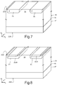
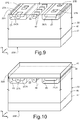
Figures 7-11 show cross-sectional perspective views of the device inFigures 3 and 4 , in successive manufacturing steps; -
Figure 12 shows a cross-sectional perspective view of the present device according to another embodiment; -
Figure 13 shows a view from above of the device ofFigure 12 ; -
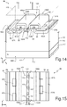
Figure 14 shows a cross-sectional perspective view of the present device according to a further embodiment; -
Figure 15 shows a view from above of the device according toFigure 14 ; and -
Figure 16 shows a view from above, with layers removed for clarity, of one alternative embodiment of the present device. -
Figures 3-5 show adevice 20 including aMOSFET transistor 54 and a JBS (Junction-Barrier Schottky)diode 53, in parallel with the MOSFET transistor 54 (see, in particular, the electrical equivalent inFigure 5 ). - As shown in detail in
Figures 3 and 4 , thedevice 20 is formed here in abody 22, of silicon carbide, with a first conductivity type (for example, of the N type), having anupper surface 22A and alower surface 22B. - The
body 22 is formed by a substrate 47 (defining thelower surface 22B) and by an epitaxial layer 46 (defining theupper surface 22A). - The
body 22 accommodates a first and asecond body region body regions upper surface 22A into the interior of the body 22 (in a direction parallel to a second axis Z of the reference frame XYZ). - The
body regions body 22 an intermediate region, henceforth referred to as the JFET (Junction Field-Effect Transistor)region 35, facing theupper surface 22A. The JFETregion 35 accommodates a plurality of implantedregions 40, of the P type, extending into the interior of thebody 22 from theupper surface 22A. - The implanted
regions 40 have a width W1, in a direction parallel to a third axis X of the reference frame XYZ, less than the distance between thebody regions regions 40 are mutually aligned in a direction parallel to the first axis Y and bound between them a plurality ofintermediate contact portions 37 of theJFET region 35; furthermore, each implantedregion 40 is equispaced from the successive one and from the preceding one in a direction parallel to the first axis Y (for example, each implantedregion 40 may be separated from the adjacent implanted regions by a distance in the range between 0.5 µm and 5 µm, in particular equal to 1 µm). - The
body regions second source region upper surface 22A into the interior of thebody regions - A plurality of enriched
regions 27A-27D, of the P type and with a high doping level (for example, greater than 5·1018 atoms/cm3) extends from thefirst surface 22A of thebody 22 into the interior of thesource regions body regions - In particular, the
enriched regions 27A-27D comprise first enrichedregions Figure 4 ), extending through thefirst source region 24 and mutually aligned in a direction parallel to the first axis Y, and second enrichedregions second source region 26 and mutually aligned in a direction parallel to the first axis Y (as can in particular be seen inFigure 4 ). - In the exemplary embodiment shown, the first enriched
regions regions Figure 4 ). As shown inFigure 3 , on theupper surface 22A, a first and a secondinsulating region - In detail, the first
insulating region 28 lies partially over the implantedregions 40, extending on top of afirst JFET portion 38A and, partially, on top of thefirst source region 24 and of thefirst body region 23. In an analogous manner, the secondinsulating region 31 lies partially over the implantedregions 40, extending on top of asecond JFET portion 38B and, partially, on top of thesecond source region 26 and of thesecond body region 25. - A first and a second
conductive region insulating region device 20. A first and a seconddielectric region conductive region - The first
insulating region 28, the firstconductive region 29 and the firstdielectric region 30 form a firstisolated gate region 36A; the secondinsulating region 31, the secondconductive region 32 and the seconddielectric region 33 form a secondisolated gate region 36B. The first and the secondisolated gate regions gate structure 39. - As can be seen in particular in
Figure 4 , the first and the secondisolated gate region gap 45 having a width W2, for example, smaller than the width W1 of the implantedregions 40. - Furthermore, an upper metallization layer 43 (shown in transparency in
Figure 3 ) extends over the entireupper surface 22A and alower metallization layer 44 extends over the entirelower surface 22B, in such a manner as to allow the electrical connection and the operation of thedevice 20. - In particular, the
lower metallization layer 44, in contact with thebody 22, forms the drain terminal D of thedevice 20. - The
upper metallization layer 43 forms a source terminal S of thedevice 20, in direct contact with thesource regions upper metallization layer 43 extends between theisolated gate regions gap 45, where it is in contact with both the implantedregions 40 in theJFET region 35, here forming an ohmic contact, and with theintermediate contact portions 37, here forming a Schottky contact. Thedevice 20 inFigures 3-4 (the electrical equivalent can be seen inFigure 5 ) thus forms aJBS diode 53 in parallel with theMOSFET transistor 54, the latter being formed by thebody 22, by thesource regions gate structure 39. - With reference to
Figure 5 , theJBS diode 53 has its cathode terminal coupled to afirst conduction node 56 and its anode terminal coupled to asecond conduction node 58. For example, thefirst conduction node 56 may be a power supply node and the second conduction node may be coupled to a ground line. As an alternative, if thedevice 20 is used in a bridge structure, theconduction nodes - The
MOSFET transistor 54 has a gate terminal G designed to receive a control signal s1, a drain terminal D coupled to thefirst conduction node 56 and a source terminal S coupled to thesecond conduction node 58. Furthermore, the source terminal S is short-circuited with thebody regions MOSFET transistor 54. - Furthermore, as indicated, the
JBS diode 53 is formed by the electrical contact between theupper metallization layer 43, the implantedregions 40 and theintermediate portions 37 inFigures 3 and 4 . - In use, in a first phase, the control signal s1 is high and commands the
MOSFET transistor 54 to turn on; as a result, theMOSFET transistor 54 conducts, allowing a current I to flow from thefirst conduction node 56 to thesecond conduction node 58, through theMOSFET transistor 54. In this first phase, theJBS diode 53 is nonconducting. - In a second phase, the control signal s1 is low and the
MOSFET transistor 54 is off. In contrast, in this second phase, theJBS diode 53 is conducting and, accordingly, a current I' can flow from thesecond conduction node 58 to thefirst conduction node 56 through theJBS diode 53. - In this mode, the
device 20 may advantageously be used in bridge structures in which it is desired for theMOSFET transistor 54 and theJBS diode 53 to work alternately. - The
device 20 described offers the following advantages. It has a high efficiency by virtue of the presence of theJBS diode 53 inFigure 5 which allows the ignition voltage of the device to be reduced, as shown inFigure 6 , illustrating the voltage-current characteristic in the case of a conventional MOSFET transistor (curve A) and in the case of the device 20 (curve B). - Furthermore, the described
device 20 offers reduced manufacturing costs compared with discrete solutions, wherein a MOSFET transistor and a diode are disposed within separate wafers and reunited in the same package. - The
device 20 inFigures 3 and 4 may be manufactured as shown inFigures 7-11 . - In
Figure 7 , using known masking and implantation techniques, doping ionic species of the P type (for example, aluminium) are implanted into thebody 22 in such a manner as to form thebody regions - For example, these implantations may take place at a dose in the range between 5·1013 and 5·1014 atoms/cm2, in particular equal to 1·1014 atoms/cm2 with an implantation energy in the range between 20 and 600 keV. In this way, inside the
body 22, between thebody regions JFET region 35 is formed. - Subsequently, in
Figure 8 , using known masking and implantation techniques, an implantation of doping ionic species of the N type, such as nitrogen or phosphorous, is carried out in such a manner as to form thefirst source region 24 in thefirst body region 23 and thesecond source region 26 in thesecond body region 25. For example, this implantation may take place at a dose in the range between 5·1014 and 1·1016 atoms/cm2, in particular equal to 5·1015 atoms/cm2, with an implantation energy, for example, in the range between 20 keV and 300 keV. - With reference to
Figure 9 , simultaneously and using a single mask, the implantation of doping ionic species of the P type (for example, aluminium) into the implantedregions 40 and into the enrichedregions 27A-27D is carried out by means of known masking and implantation techniques. For example, this implantation may take place at a dose in the range between 5·1014 and 1.1016 atoms/cm2, in particular equal to 5·e15 atoms/cm2 (with an implantation energy in the range between 20 keV and 300 keV). - Subsequently, an activation step is carried out, wherein the
body 22 is heated to high temperature (for example in the range between 1600°C and 1800°C, in particular to 1700°C) in order to obtain the activation of the doping ionic species and to complete the implantation process. The implantedregions 40 and the enrichedregions 27A-27D thus formed exhibit a higher doping level compared withbody regions - Thus, in
Figure 10 , using known deposition techniques, agate oxide layer 41, of insulating material, for example silicon oxide, intended to form the insulatingregions upper surface 22A. Subsequently, on one surface of thegate oxide layer 41 and over its entire extension, agate layer 42, of conductive material, such as polysilicon, intended to form theconductive regions - Subsequently, in
Figure 11 , thegate layer 42 and theoxide layer 41 are defined according to known photolithographic techniques, thus forming the insulatingregions conductive regions regions conductive regions regions 40 and to the enrichedregions 27A-27D takes place by means of common "Zero Layer" techniques, namely taking advantage of the dedicated trenches in non-active regions. - Subsequently, on top of the structure thus formed, an insulating layer (not shown) is deposited and defined by means of known deposition and definition techniques, in such a manner as to form the
dielectric regions isolated gate structures gate structure 39, are thus obtained. - Thus, the
lower metallization layer 44 is deposited on thelower surface 22B and theupper metallization layer 43 is deposited on theupper surface 22A, using known deposition and definition techniques. The usual final steps thus follow, including the formation of a passivation layer, dicing, etc., obtaining, in such a manner, thedevice 20 inFigures 3 and 4 . - In this way, the
JBS diode 53 inFigure 5 may be formed in a manner integrated into the device prior to the formation of theisolated gate regions - This is obtained by modifying only three masks: the enrichment mask, which here allows the implanted
regions 40 and the enrichedregions 27A-27D to be simultaneously formed; the mask for theconductive layer isolated gate regions dielectric regions 30, 33) to be removed between theisolated gate regions Figure 5 ). - In the
device 20, the ratio between the area of the ohmic contact and the area of the Schottky contact determines the ignition point and the slope of the electrical characteristic for the MOSFET transistor when the body-drain diode is biased directly; as a result, by varying this ratio, it is possible to vary the characteristics of thedevice 20. In particular, this ratio may be varied by either modifying the relative dimensions of these areas or by modifying the geometry of the MOSFET device. - In this regard,
Figures 12-16 show embodiments having various geometries with the aim of obtaining different electrical characteristics. - In particular,
Figures 12 and 13 show another embodiment of the present device, here indicated with thereference number 60, wherein the implantedregions 40 are substituted by a single implantedregion 80 and this has a smaller width W1' (in a direction parallel to the third axis X) compared with the lateral extension of the implantedregions 40 of thedevice 20. - The
device 60 is equivalent to thedevice 20 inFigures 3 and 4 , for which parts similar to those shown and described with reference toFigures 3 and 4 are indicated inFigures 12 and 13 with reference numbers increased by 40 and will not be described any further. - In detail, the width W1' of the implanted
region 80 of thedevice 60 is smaller compared with the distance (W2' inFigure 13 ) between the isolated gate regions, here indicated with 76A, 76B, and it extends over a greater length (in a direction parallel to the first axis Y) compared with thedevice 20. For example, the implantedregion 80 of thedevice 60 may extend over practically the entire length (in a direction parallel to the first axis Y) of thedevice 60. As an alternative, if desired, the implantedregion 80 may be interrupted at some points along its length or may extend only over a part of the length (in direction Y) of thedevice 20. - In the
device 60 inFigures 12 and 13 , the portions of theJFET region 75 included between the edges of the implantedregion 80 and the edges of theisolated gate regions lateral contact regions - In practice, the implanted
region 80 has the shape of a thin strip extending inside of theJFET region 75 of thebody 62 and facing theupper surface 62A; furthermore, thelateral contact regions isolated gate regions upper metallization layer 83. - Thus, in this case, the
intermediate contact portions 37 are missing and the Schottky contact is formed between theupper metallization layer 83 and thelateral contact portions regions 40 of thedevice 20, the implantedregion 80 forms an ohmic contact with theupper metallization layer 83. -
Figures 14 and 15 show a further embodiment of the present device, here indicated with thereference number 90, comprising a plurality of implanted regions, here indicated with 110, with a width that is smaller compared with the lateral extension of the plurality of implantedregions 40 inFigures 3 and 4 . - In the
device 90, parts similar to those shown and described with reference toFigures 3 and 4 are indicated inFigures 14 and 15 with reference numbers increased by 70 and will not be described any further. - In the
device 90, the implantedregions 110 have a width W1", in a direction parallel to the third axis X, that is smaller with respect to the distance W2" between the isolated gate regions, here indicated with 106A, 106B, in a similar manner to thedevice 60 inFigures 12 and 13 . In contrast, in a similar manner toFigures 3 and 4 , the implantedregions 110 are aligned and are placed equidistant in a direction parallel to the first axis Y. - As a consequence, in the
device 90 bothintermediate contact regions 107 andlateral contact regions - Thus, also in this case, the
device 90 has both a Schottky contact (between theupper metallization layer 113 and theintermediate contact regions 107, together with thelateral contact regions upper metallization layer 113 and the implanted regions 110). -
Figure 16 shows a different embodiment of a MOSFET device, here indicated with thereference number 130, having a configuration with hexagonal cells. InFigure 16 , for clarity of the figure, the upper metallization layer (13 inFigure 1 ) has not been shown. - The
device 130 is conceptually analogous to thedevice 20 inFigures 3 and 4 ; thus, elements common to thedevice 20 have been indicated, inFigure 15 , with reference numbers increased by 110. - In detail, a
body 132, of silicon carbide and with the first conductivity type, accommodates a plurality of implantedregions 150 of the P type. - Each implanted
region 150 is formed by a series ofhexagonal frames 150A, disposed aligned to one another in a direction parallel to the third axis X and each having a pair oftransverse sides 144, opposing one another and directed in a direction parallel to the first axis Y. Thetransverse sides 144 of eachhexagonal frame 150A are contiguous at thetransverse sides 144 of the two adjacenthexagonal frames 150A (or, in other words, two adjacenthexagonal frames 150A share a transverse side 144), thus forming a plurality of strips extending parallel to the third axis X. Eachhexagonal frame 150A surrounds, in a concentric manner and with a gap, a body region 133' and a source region 134'; furthermore, within every otherhexagonal frame 150A, an enriched region 137' is present. - In detail, each body region 133' (of the P type) is of hexagonal shape and accommodates inside it a respective source region 134' (of the N type), these also being of hexagonal shape but having a smaller area than the body region 133'. The enriched regions 137' (of the P type) are disposed between every other source region 134', inside of the same, and these also have a hexagonal shape, but with a smaller area than the respective source region 134'. The body region 133', source region 134' and enriched region 137' are furthermore concentric and have mutually parallel sides.
- On top of each area of the
body 132 that accommodates thehexagonal frames 150A, a respective isolated gate region is present, here indicated with the reference number 146', of thedevice 130. In a similar manner to the preceding figures, each gate structure 146' comprises an insulating region, a conductive region and a dielectric region (not shown). - Each isolated gate region 146' has the shape of a hexagonal ring having a smaller outer perimeter as compared with the perimeter of the respective
hexagonal frame 150A; furthermore, each isolated gate region 146' is concentric, when viewed from the top, with the respectivehexagonal frame 150A and with the respective body region 133', source region 134' and enriched region 137' (where provided). In detail, each isolated gate region 146' is superposed onto the portion of the respective body region 133' facing the first surface (annular region seen inFigure 16 ) and a peripheral portion of the respective source region 134'. As a consequence, the internal parts of the source regions 134' facing the first surface and the enriched regions 137' (where present) are not covered by the isolated gate region 146' and are in direct contact with the first metallization layer (not shown), forming a JBS diode (53 inFigure 5 ), in a similar manner to what was discussed with reference toFigures 3-4 . - Between adjacent pairs of strips of implanted
regions 150, portions of thebody 132 are present that do not have the implanted regions but accommodatebody regions 133",source regions 134" and enrichedregions 137". Thebody regions 133",source regions 134" and enrichedregions 137" are disposed in a similar manner to the body regions 133', source regions 134' and enriched regions 137', but are offset by a half-step in a direction parallel to the third axis X. On top of thebody region 133" andsource region 134",isolated gate regions 146" are present having exactly the same shape and disposition of the isolated gate regions 146' described above. - In this manner, laterally to the implanted
regions 150, portions of thebody 132 are present facing the first surface of the body itself. These portions of thebody 132form JFET regions 145 analogous to theJFET regions 35 inFigures 3-4 . In practice, theJFET regions 145 have the shape of a hexagonal ring surrounding, in the view from above inFigure 16 , theisolated gate regions 146', 146". - The result of this is that the metallization layer (not shown) in direct contact with the
JFET regions 145 and with the implantedregions 150 form JBS diodes, in a manner analogous to what was described for thedevices - Finally, it is clear that modifications and variants may be applied to the device and process described and illustrated here without however straying from the scope of protection of the present invention, as defined in the appended claims.
- In particular, the isolated gate structures may have a different shape; for example they may have circular or different polygonal shapes with respect to that shown in
Figure 16 . - Furthermore, in the embodiment in
Figure 16 , portions of the implantedregion 150 may extend in a direction parallel to the first axis Y from the corners of eachhexagonal frame 150A as far as corresponding corners of an adjacent strip. In practice, in this way, the implantedregion 150 no longer forms strips, but extends in a honeycomb over the whole plane XY. - The enriched
regions 27A-27D may also be disposed in a manner different from what is shown, both as regards their lateral extension (direction Y) and as regards their staggering.
Claims (17)
- An integrated MOSFET device (20; 60; 90; 130) comprising:a body (22; 62; 92; 132), of silicon carbide and with a first conductivity type, having a first surface (22A; 62A; 92A) and a second surface (22B; 62B; 92B);a first body region (23; 63; 93; 133'), with a second conductivity type, extending from the first surface (22A; 62A; 92A) into the interior of the body (22; 62; 92; 132);a JFET region (35; 75; 105; 145) adjacent to the first body region (23; 63; 93; 133') and facing the first surface (22A; 62A; 92A);a first source region (24; 64; 94; 134'), with the first conductivity type, extending from the first surface (22A; 62A; 92A) into the interior of the first body region (23; 63; 93; 133');an isolated gate structure (39; 79; 109; 146', 146"), extending over the first surface (22A; 62A; 92A) and lying partially over the first body region (23; 63; 93; 133'), the first source region (24; 64; 94; 134') and the JFET region (35; 75; 105; 145);an implanted structure (40; 80; 110; 150), with the second conductivity type, extending into the interior of the JFET region (35; 75; 105; 145) from the first surface (22A; 62A; 92A); anda first metallization layer (43; 83; 113) extending over the first surface (22A; 62A; 92A), the first metallization layer (43; 83; 113) being in direct contact with the implanted structure (40; 80; 110; 150) and with the JFET region (35; 75; 105; 145) and forming a JBS diode (53) .
- A device according to claim 1, furthermore comprising:a second body region (25; 65; 95; 133"), with the second conductivity type, extending from the first surface (22A; 62A; 92A) into the interior of the body (22; 62; 92; 132), the JFET region (35; 75; 105; 145) being disposed between the first (23; 63; 93; 133') and the second body regions (25; 65; 95; 133");a second source region (26; 66; 96; 134"), with the first conductivity type, extending from the first surface (22A; 62A; 92A) into the interior of the second body region (25; 65; 95; 133");the isolated gate structure (39; 79; 109; 146', 146") comprising at least a first isolated gate region (36A; 76A; 106A; 146') and a second isolated gate region (36B; 76B; 106B; 146"), the first isolated gate region (36A; 76A; 106A; 146') lying partially over the first body region (23; 63; 93; 133'), the first source region (24; 64; 94; 134') and the JFET region, the second isolated gate region (36B; 76B; 106B; 146") lying partially over the second body region (25; 65; 95; 133"), the second source region (26; 66; 96; 134") and the JFET region (35; 75; 105; 145), the first (36A; 76A; 106A; 146') and the second isolated gate region (36B; 76B; 106B; 146") being separated by a gap (45; 85; 115) having a width in a first direction and lying over a portion of the JFET region, the portion of the JFET region (35; 75; 105; 145) being disposed below the gap accommodating the implanted structure (40; 80; 110; 150).
- A device according to claim 2, furthermore comprising:at least a first enriched region (27A, 27C; 67A, 67C; 97A, 97C; 137'), with the second conductivity type, extending from the first surface (22A; 62A; 92A) into the interior of the first source region (23; 63; 93; 134');at least a second enriched region (27B, 27D; 67B, 67D; 97B, 97D; 137"), with the second conductivity type, extending from the first surface (22A; 62A; 92A) into the interior of the second source region (25; 65; 95; 134"), the first (27A, 27C; 67A, 67C; 97A, 97C; 137') and the second enriched regions (27B, 27D; 67B, 67D; 97B, 97D; 137") being mutually offset in a second direction transverse to the first direction.
- A device according to any one of the preceding claims, furthermore comprising a second metallization layer (44; 84; 114), extending over the second surface (22B; 62B; 92B) of the body (22; 62; 92; 132).
- A device according to claim 2, wherein the implanted structure (40; 80; 110; 150) comprises a plurality of implanted regions (40; 110) mutually separated by intermediate portions (37; 107) of the JFET region (35; 105) in a second direction, transverse to the first direction, the first metallization layer (43; 113) forming an ohmic contact with the implanted regions (40; 110) and a Schottky contact with the intermediate portions (37; 107).
- A device according to claim 5, wherein the implanted regions (40) have a greater extension in the first direction compared with the width of the gap (45) and are partially covered by the first (36A) and by the second isolated gate regions (36B).
- A device according to claim 5, wherein the implanted regions (80; 110) have a shorter extension in the first direction with respect to the width of the gap (85; 115) and bound lateral portions (78A, 78B; 108A; 108B) of the JFET region (75; 105) not covered by the isolated gate regions (76B; 106B), the first metallization layer (83; 113) forming a further Schottky contact with the lateral portions (78A, 78B; 108A, 108B).
- A device according to claim 2, wherein the implanted structure (80; 150) comprises a strip region extending in a second direction transverse to the first direction.
- A device according to claim 8, wherein the strip region has a shorter extension in the first direction compared with the width of the gap (85) and bounds lateral portions (78A, 78B) of the JFET region (75) not covered by the isolated gate regions (76A, 76B), the first metallization layer (83) forming an ohmic contact with the strip region and a Schottky contact with the lateral portions (78A, 78B).
- A device according to claim 2, wherein the first (146') and the second isolated gate region (146") have a closed annular shape and comprise portions surrounding, when viewed from above, the respective first (133') and second body region (133") and the implanted structure (150) comprises at least a first implanted region (150A) surrounding, when viewed from above, the first isolated gate region (146') and bounding lateral portions of the JFET region (145) not covered by the isolated gate regions (146', 146"), the first metallization layer forming an ohmic contact with the first implanted region (150) and a Schottky contact with the lateral portions.
- A device according to claim 10, wherein the gate structure (146', 146") comprises further isolated gate regions (146') aligned with the first isolated gate region (146') in a second direction transverse with respect to the first direction, the further isolated gate regions (146') having a closed annular shape and comprising portions surrounding, when viewed from above, respective further body regions (133') and respective further source regions (134'), and the implanted structure (150) furthermore comprises further implanted regions (150) surrounding, when viewed from above, respective isolated gate regions (146') and bounding further lateral portions of the JFET region (145) not covered by the further isolated gate regions (146'), the first metallization layer forming ohmic contacts with the further implanted regions (150) and Schottky contacts with the further lateral portions (145).
- A device according to claim 11, comprising at least one of the following characteristics:the first implanted region (150) and the further implanted regions (150) are mutually connected in the second direction and have shared sides (144);some of the further source regions (134') accommodate further enriched regions (137') with the second conductivity type, the first enriched region (137') and the further enriched regions (137') being disposed alternately between every other source region (134') in the second direction;the first, the second and the further isolated gate regions (146', 146"), the first, the second and the further implanted regions (150) have a hexagonal ring shape, the first, the second and the further body regions (133', 133"), the first, the second and the further source regions (134', 134") and the first, the second and the further enriched regions (137', 137") have a hexagonal shape.
- A manufacturing process for an integrated MOSFET device (20; 60; 90; 130) comprising:in a body (22; 62; 92; 132) of silicon carbide and having a first conductivity type, a first surface (22A; 62A; 92A) and a second surface (22B; 62B; 92B), forming a first body region (23; 63; 93; 133'), having a second conductivity type, from the first surface (22A; 62A; 92A) into the interior of the body (22; 62; 92; 132), the first body region bounding, inside of the body, a JFET region (35; 75; 105; 145) facing the first surface;forming a first source region (24; 64; 94; 134'), with the first conductivity type, from the first surface (22A; 62A; 92A) into the interior of the first body region (23; 63; 93; 133');forming an implanted structure (40; 80; 110; 150), with the second conductivity type, inside of the JFET region (35; 75; 105; 145), from the first surface (22A; 62A; 92A);forming an isolated gate structure (39; 79; 109; 146', 146"), on the first surface (22A; 62A; 92A) in a position partially overlying the first body region (23; 63; 93; 133'), the first source region (24; 64; 94; 134') and the JFET region (35; 75; 105; 145); andforming a first metallization layer (43; 83; 113) on the first surface in direct contact with the implanted structure (40; 80; 110; 150) and with the JFET region (35; 75; 105; 145), forming a JBS diode (53).
- A process according to claim 13, further comprising:forming a second body region (25; 65; 95; 133"), with the second conductivity type, from the first surface (22A; 62A; 92A) into the interior of the body (22; 62; 92; 132), laterally to the JFET region (35; 75; 105; 145);forming a second source region (26; 66; 96; 134"), with the first conductivity type, from the first surface (22A; 62A; 92A) into the interior of the second body region (25; 65; 95; 133");wherein forming the isolated gate structure (39; 79; 109; 146', 146") comprises forming a first isolated gate region (36A; 76A; 96A; 146') and a second isolated gate region (36B; 76B; 96B; 146"),the first isolated gate region (36A; 76A; 96A; 146') lying partially over the first body region (23; 63; 93; 133'), the first source region (24; 64; 94; 134') and the JFET region (35; 75; 105; 145),the second isolated gate region (36B; 76B; 96B; 146") lying partially over the second body region (25; 65; 95; 133"), the second source region (26; 66; 96; 134") and the JFET region (35; 75; 105; 145),the first (36A; 76A; 96A; 146') and the second isolated gate regions (36B; 76B; 96B; 146") being separated by a gap (45; 85; 115) having a length in a first direction, the JFET region (35; 75; 105; 145) disposed below the gap (45; 85; 115) accommodating the implanted structure (40; 80; 110; 150).
- A process according to claim 14, further comprising:forming at least a first enriched region (27A, 27C; 67A, 67C; 97A, 97C; 137'), with the second conductivity type, from the first surface (22A; 62A; 92A) into the interior of the first source region (23; 63; 93; 134'); andforming at least a second enriched region (27B, 27D; 67A, 67D; 97B, 97D; 137") having the second conductivity type, from first surface (22A; 62A; 92A) into the interior of the second source region (25; 65; 95; 134"), the first (27A, 27C; 67A, 67C; 97A, 97C; 137') and the second enriched region (27B, 27D; 67A, 67D; 97B, 97D; 137") being mutually offset in a second direction transverse to the first direction.
- A process according to claim 15, wherein forming an implanted structure (40; 80; 110; 150), forming the first enriched region (27A, 27C; 67A, 67C; 97A, 97C; 137') and forming the second enriched region (27B, 27D; 67A, 67D; 97B, 97D; 137") comprise implanting doping ionic species.
- A process according to any of claims 13-16, further comprising:
forming a lower metallization layer (44; 84; 114) on the second surface (22B; 62B; 92B) of the body (22; 62; 92; 132) .
Applications Claiming Priority (1)
| Application Number | Priority Date | Filing Date | Title |
|---|---|---|---|
| IT102017000073767A IT201700073767A1 (en) | 2017-07-05 | 2017-07-05 | SILICON CARBIDE MOSFET DEVICE WITH AN INTEGRATED DIODE AND RELATIVE PROCESS OF MANUFACTURE |
Publications (2)
| Publication Number | Publication Date |
|---|---|
| EP3425676A1 true EP3425676A1 (en) | 2019-01-09 |
| EP3425676B1 EP3425676B1 (en) | 2022-12-28 |
Family
ID=60183018
Family Applications (1)
| Application Number | Title | Priority Date | Filing Date |
|---|---|---|---|
| EP18181848.5A Active EP3425676B1 (en) | 2017-07-05 | 2018-07-05 | Mosfet device of silicon carbide having an integrated diode and manufacturing process thereof |
Country Status (4)
| Country | Link |
|---|---|
| US (4) | US10707202B2 (en) |
| EP (1) | EP3425676B1 (en) |
| CN (2) | CN109216351B (en) |
| IT (1) | IT201700073767A1 (en) |
Families Citing this family (25)
| Publication number | Priority date | Publication date | Assignee | Title |
|---|---|---|---|---|
| IT201700073767A1 (en) * | 2017-07-05 | 2019-01-05 | St Microelectronics Srl | SILICON CARBIDE MOSFET DEVICE WITH AN INTEGRATED DIODE AND RELATIVE PROCESS OF MANUFACTURE |
| CN110459540B (en) * | 2019-07-30 | 2021-10-26 | 创能动力科技有限公司 | Semiconductor device integrating MOSFET and diode and method for manufacturing the same |
| US10777689B1 (en) * | 2019-10-18 | 2020-09-15 | Hong Kong Applied Science and Technology Research Institute Company, Limited | Silicon-carbide shielded-MOSFET embedded with a trench Schottky diode and heterojunction gate |
| US12328932B2 (en) * | 2020-02-06 | 2025-06-10 | Lg Electronics Inc. | Metal-oxide semiconductor field effect transistor device and manufacturing method therefor |
| CN111446293A (en) * | 2020-03-25 | 2020-07-24 | 浙江大学 | Silicon carbide power MOSFET device of enhanced body diode |
| US11004940B1 (en) | 2020-07-31 | 2021-05-11 | Genesic Semiconductor Inc. | Manufacture of power devices having increased cross over current |
| CA3191358A1 (en) | 2020-08-31 | 2022-03-03 | Genesic Semiconductor Inc. | Design and manufacture of improved power devices |
| CN112271220B (en) * | 2020-10-10 | 2025-02-07 | 安徽芯塔电子科技有限公司 | A trench type Schottky diode device |
| IT202000032441A1 (en) * | 2020-12-24 | 2022-06-24 | Consiglio Nazionale Ricerche | SILICON CARBIDE MOSFET TRANSISTOR DEVICE HAVING IMPROVED CHARACTERISTICS AND RELATED MANUFACTURING PROCESS |
| CN114678424A (en) * | 2020-12-24 | 2022-06-28 | 意法半导体股份有限公司 | Silicon carbide MOSFET transistor device with improved characteristics and corresponding method of fabrication |
| US20230387290A1 (en) * | 2021-02-25 | 2023-11-30 | Xiamen San'an Integrated Circuit Co., Ltd. | Silicon carbide metal oxide semiconductor field effect transistor device |
| JP7515719B2 (en) * | 2021-06-09 | 2024-07-12 | 三菱電機株式会社 | Silicon carbide semiconductor device |
| CN114220844B (en) * | 2021-12-15 | 2025-12-02 | 株洲中车时代半导体有限公司 | Silicon carbide MOSFET device with integrated SBD and its fabrication method |
| CN115084271B (en) * | 2022-07-08 | 2025-02-14 | 深圳市坪芯微电子有限公司 | A silicon carbide power device and a processing and manufacturing method thereof |
| CN115394856A (en) * | 2022-09-21 | 2022-11-25 | 南方科技大学 | Super junction MOSFET and preparation method thereof |
| CN115241282B (en) * | 2022-09-23 | 2023-01-10 | 浙江大学杭州国际科创中心 | SiC MOSFET device and preparation method thereof |
| CN115832026A (en) * | 2022-12-05 | 2023-03-21 | 上海积塔半导体有限公司 | Semiconductor structure and its preparation method |
| CN115579399A (en) * | 2022-12-12 | 2023-01-06 | 深圳平创半导体有限公司 | A Silicon Carbide MOSFET Cellular Layout Structure |
| CN115799344A (en) * | 2023-02-03 | 2023-03-14 | 深圳平创半导体有限公司 | A kind of silicon carbide JFET cell structure and its manufacturing method |
| CN116314290A (en) * | 2023-03-14 | 2023-06-23 | 广东芯粤能半导体有限公司 | Semiconductor device and manufacturing method thereof |
| WO2024206640A1 (en) * | 2023-03-28 | 2024-10-03 | Purdue Research Foundation | Vertical dmosfets with buried shield for reduced gate-to-drain charge |
| US20250113531A1 (en) * | 2023-09-28 | 2025-04-03 | Wolfspeed, Inc. | Power silicon carbide based semiconductor devices with selective jfet implants that are self-aligned with the well regions and methods of making such devices |
| CN117253923A (en) * | 2023-11-20 | 2023-12-19 | 深圳平创半导体有限公司 | JBS-integrated boss split-gate silicon carbide MOSFET and its preparation process |
| CN119545860B (en) * | 2024-11-27 | 2025-09-30 | 湖北九峰山实验室 | Trench MOSFET device with integrated junction controlled diode and electronic device |
| CN119545862B (en) * | 2025-01-21 | 2025-04-29 | 西安龙飞电气技术有限公司 | Anti-radiation super junction power MOS device and preparation method thereof |
Citations (9)
| Publication number | Priority date | Publication date | Assignee | Title |
|---|---|---|---|---|
| EP0867943A1 (en) * | 1997-03-28 | 1998-09-30 | STMicroelectronics, Inc. | DMOS transistors with schottky diode body structure |
| EP1432037A2 (en) | 2002-12-20 | 2004-06-23 | STMicroelectronics S.r.l. | Integrated device with Schottky diode and with MOS transistor and related manufacturing process |
| US6979863B2 (en) * | 2003-04-24 | 2005-12-27 | Cree, Inc. | Silicon carbide MOSFETs with integrated antiparallel junction barrier Schottky free wheeling diodes and methods of fabricating the same |
| JP2009088326A (en) * | 2007-10-01 | 2009-04-23 | Fuji Electric Device Technology Co Ltd | Semiconductor device |
| US20130313570A1 (en) | 2012-05-24 | 2013-11-28 | Microsemi Corporation | Monolithically integrated sic mosfet and schottky barrier diode |
| US20150270354A1 (en) * | 2014-03-20 | 2015-09-24 | Kabushiki Kaisha Toshiba | Semiconductor device and method for producing the same |
| US20160027878A1 (en) * | 2014-07-24 | 2016-01-28 | Sumitomo Electric Industries, Ltd. | Silicon carbide semiconductor device |
| WO2016185544A1 (en) * | 2015-05-18 | 2016-11-24 | 株式会社日立製作所 | Semiconductor device and power conversion device |
| US20170133503A1 (en) * | 2015-02-11 | 2017-05-11 | Monolith Semiconductor Inc. | High voltage semiconductor devices and methods of making the devices |
Family Cites Families (13)
| Publication number | Priority date | Publication date | Assignee | Title |
|---|---|---|---|---|
| JP2007059636A (en) * | 2005-08-25 | 2007-03-08 | Renesas Technology Corp | DMOSFET and planar type MOSFET |
| WO2013172059A1 (en) * | 2012-05-15 | 2013-11-21 | 富士電機株式会社 | Semiconductor device |
| US9111919B2 (en) * | 2013-10-03 | 2015-08-18 | Cree, Inc. | Field effect device with enhanced gate dielectric structure |
| US10483389B2 (en) * | 2014-07-02 | 2019-11-19 | Hestia Power Inc. | Silicon carbide semiconductor device |
| TWI528565B (en) * | 2014-07-02 | 2016-04-01 | 瀚薪科技股份有限公司 | Silicon carbide semiconductor components |
| DE112015004093B4 (en) * | 2015-01-16 | 2023-09-28 | Fuji Electric Co., Ltd. | SILICON CARBIDE SEMICONDUCTOR DEVICE AND METHOD FOR PRODUCING A SILICON CARBIDE SEMICONDUCTOR DEVICE |
| JP6309656B2 (en) * | 2015-02-12 | 2018-04-11 | 株式会社日立製作所 | Semiconductor device and manufacturing method thereof, power conversion device, three-phase motor system, automobile and railway vehicle |
| US9324807B1 (en) * | 2015-07-10 | 2016-04-26 | United Silicon Carbide, Inc. | Silicon carbide MOSFET with integrated MOS diode |
| US10243039B2 (en) * | 2016-03-22 | 2019-03-26 | General Electric Company | Super-junction semiconductor power devices with fast switching capability |
| US11075264B2 (en) * | 2016-05-31 | 2021-07-27 | Cree, Inc. | Super junction power semiconductor devices formed via ion implantation channeling techniques and related methods |
| CN109478569B (en) * | 2016-07-21 | 2022-02-22 | 三菱电机株式会社 | Silicon carbide semiconductor device and method for manufacturing silicon carbide semiconductor device |
| JP6666224B2 (en) * | 2016-09-21 | 2020-03-13 | 株式会社東芝 | Semiconductor device |
| IT201700073767A1 (en) * | 2017-07-05 | 2019-01-05 | St Microelectronics Srl | SILICON CARBIDE MOSFET DEVICE WITH AN INTEGRATED DIODE AND RELATIVE PROCESS OF MANUFACTURE |
-
2017
- 2017-07-05 IT IT102017000073767A patent/IT201700073767A1/en unknown
-
2018
- 2018-07-03 US US16/027,060 patent/US10707202B2/en active Active
- 2018-07-03 CN CN201810719162.9A patent/CN109216351B/en active Active
- 2018-07-03 CN CN201821044765.5U patent/CN208796997U/en active Active
- 2018-07-05 EP EP18181848.5A patent/EP3425676B1/en active Active
-
2020
- 2020-02-03 US US16/780,769 patent/US11270993B2/en active Active
-
2022
- 2022-02-02 US US17/591,534 patent/US11916066B2/en active Active
-
2024
- 2024-01-18 US US18/416,702 patent/US20240243122A1/en active Pending
Patent Citations (10)
| Publication number | Priority date | Publication date | Assignee | Title |
|---|---|---|---|---|
| EP0867943A1 (en) * | 1997-03-28 | 1998-09-30 | STMicroelectronics, Inc. | DMOS transistors with schottky diode body structure |
| EP1432037A2 (en) | 2002-12-20 | 2004-06-23 | STMicroelectronics S.r.l. | Integrated device with Schottky diode and with MOS transistor and related manufacturing process |
| US6979863B2 (en) * | 2003-04-24 | 2005-12-27 | Cree, Inc. | Silicon carbide MOSFETs with integrated antiparallel junction barrier Schottky free wheeling diodes and methods of fabricating the same |
| JP2009088326A (en) * | 2007-10-01 | 2009-04-23 | Fuji Electric Device Technology Co Ltd | Semiconductor device |
| US20130313570A1 (en) | 2012-05-24 | 2013-11-28 | Microsemi Corporation | Monolithically integrated sic mosfet and schottky barrier diode |
| US20150270354A1 (en) * | 2014-03-20 | 2015-09-24 | Kabushiki Kaisha Toshiba | Semiconductor device and method for producing the same |
| US20160027878A1 (en) * | 2014-07-24 | 2016-01-28 | Sumitomo Electric Industries, Ltd. | Silicon carbide semiconductor device |
| US20170133503A1 (en) * | 2015-02-11 | 2017-05-11 | Monolith Semiconductor Inc. | High voltage semiconductor devices and methods of making the devices |
| WO2016185544A1 (en) * | 2015-05-18 | 2016-11-24 | 株式会社日立製作所 | Semiconductor device and power conversion device |
| DE112015005384T5 (en) * | 2015-05-18 | 2017-10-05 | Hitachi, Ltd. | SEMICONDUCTOR DEVICE AND POWER IMPLEMENTING DEVICE |
Also Published As
| Publication number | Publication date |
|---|---|
| US20200176442A1 (en) | 2020-06-04 |
| US11916066B2 (en) | 2024-02-27 |
| IT201700073767A1 (en) | 2019-01-05 |
| US20190013312A1 (en) | 2019-01-10 |
| CN109216351B (en) | 2023-06-27 |
| US20220157807A1 (en) | 2022-05-19 |
| US20240243122A1 (en) | 2024-07-18 |
| US10707202B2 (en) | 2020-07-07 |
| CN109216351A (en) | 2019-01-15 |
| CN208796997U (en) | 2019-04-26 |
| EP3425676B1 (en) | 2022-12-28 |
| US11270993B2 (en) | 2022-03-08 |
Similar Documents
| Publication | Publication Date | Title |
|---|---|---|
| EP3425676B1 (en) | Mosfet device of silicon carbide having an integrated diode and manufacturing process thereof | |
| CN101719495B (en) | Semiconductor device and manufacturing method thereof | |
| KR100256903B1 (en) | Field effect transistor | |
| US7649223B2 (en) | Semiconductor device having superjunction structure and method for manufacturing the same | |
| CA3191367C (en) | Design and manufacture of improved power devices | |
| US20180019309A1 (en) | Semiconductor device based on wideband gap semiconductor materials | |
| US8890169B2 (en) | Semiconductor device | |
| JP2005501408A (en) | Trench double-diffused metal oxide semiconductor transistor incorporating a trench Schottky rectifier | |
| US12074079B2 (en) | Wide bandgap semiconductor device with sensor element | |
| CN111816694B (en) | Superjunction semiconductor device and method for manufacturing superjunction semiconductor device | |
| US11004839B1 (en) | Trench power MOSFET with integrated-schottky in non-active area | |
| CN112466922A (en) | Semiconductor device with a plurality of semiconductor chips | |
| US10147813B2 (en) | Tunneling field effect transistor | |
| KR102832585B1 (en) | Wide bandgap semiconductor device with sensor element | |
| US20250203977A1 (en) | Silicon carbide vertical conduction mosfet device for power applications and manufacturing process thereof | |
| US12255233B2 (en) | Silicon carbide vertical conduction MOSFET device for power applications and manufacturing process thereof | |
| US20240379667A1 (en) | Wide bandgap semiconductor device with sensor element | |
| CA3191347C (en) | Design and manufacture of improved power devices | |
| JP7806006B2 (en) | Design and manufacture of improved power devices | |
| KR20250039309A (en) | Semiconductor switching device | |
| JP2026081273A (en) | Design and manufacturing of improved power devices |
Legal Events
| Date | Code | Title | Description |
|---|---|---|---|
| PUAI | Public reference made under article 153(3) epc to a published international application that has entered the european phase |
Free format text: ORIGINAL CODE: 0009012 |
|
| STAA | Information on the status of an ep patent application or granted ep patent |
Free format text: STATUS: THE APPLICATION HAS BEEN PUBLISHED |
|
| AK | Designated contracting states |
Kind code of ref document: A1 Designated state(s): AL AT BE BG CH CY CZ DE DK EE ES FI FR GB GR HR HU IE IS IT LI LT LU LV MC MK MT NL NO PL PT RO RS SE SI SK SM TR |
|
| AX | Request for extension of the european patent |
Extension state: BA ME |
|
| STAA | Information on the status of an ep patent application or granted ep patent |
Free format text: STATUS: REQUEST FOR EXAMINATION WAS MADE |
|
| 17P | Request for examination filed |
Effective date: 20190708 |
|
| RBV | Designated contracting states (corrected) |
Designated state(s): AL AT BE BG CH CY CZ DE DK EE ES FI FR GB GR HR HU IE IS IT LI LT LU LV MC MK MT NL NO PL PT RO RS SE SI SK SM TR |
|
| STAA | Information on the status of an ep patent application or granted ep patent |
Free format text: STATUS: EXAMINATION IS IN PROGRESS |
|
| 17Q | First examination report despatched |
Effective date: 20210423 |
|
| RIC1 | Information provided on ipc code assigned before grant |
Ipc: H01L 29/16 20060101ALI20220607BHEP Ipc: H01L 29/06 20060101ALI20220607BHEP Ipc: H01L 29/872 20060101ALI20220607BHEP Ipc: H01L 21/336 20060101ALI20220607BHEP Ipc: H01L 29/78 20060101AFI20220607BHEP |
|
| GRAP | Despatch of communication of intention to grant a patent |
Free format text: ORIGINAL CODE: EPIDOSNIGR1 |
|
| STAA | Information on the status of an ep patent application or granted ep patent |
Free format text: STATUS: GRANT OF PATENT IS INTENDED |
|
| INTG | Intention to grant announced |
Effective date: 20220721 |
|
| RIN1 | Information on inventor provided before grant (corrected) |
Inventor name: RASCUNA', SIMONE Inventor name: SAGGIO, MARIO GIUSEPPE |
|
| GRAJ | Information related to disapproval of communication of intention to grant by the applicant or resumption of examination proceedings by the epo deleted |
Free format text: ORIGINAL CODE: EPIDOSDIGR1 |
|
| INTG | Intention to grant announced |
Effective date: 20220721 |
|
| GRAS | Grant fee paid |
Free format text: ORIGINAL CODE: EPIDOSNIGR3 |
|
| GRAA | (expected) grant |
Free format text: ORIGINAL CODE: 0009210 |
|
| STAA | Information on the status of an ep patent application or granted ep patent |
Free format text: STATUS: THE PATENT HAS BEEN GRANTED |
|
| AK | Designated contracting states |
Kind code of ref document: B1 Designated state(s): AL AT BE BG CH CY CZ DE DK EE ES FI FR GB GR HR HU IE IS IT LI LT LU LV MC MK MT NL NO PL PT RO RS SE SI SK SM TR |
|
| REG | Reference to a national code |
Ref country code: GB Ref legal event code: FG4D |
|
| REG | Reference to a national code |
Ref country code: CH Ref legal event code: EP |
|
| REG | Reference to a national code |
Ref country code: DE Ref legal event code: R096 Ref document number: 602018044648 Country of ref document: DE |
|
| REG | Reference to a national code |
Ref country code: AT Ref legal event code: REF Ref document number: 1541019 Country of ref document: AT Kind code of ref document: T Effective date: 20230115 |
|
| REG | Reference to a national code |
Ref country code: IE Ref legal event code: FG4D |
|
| REG | Reference to a national code |
Ref country code: LT Ref legal event code: MG9D |
|
| PG25 | Lapsed in a contracting state [announced via postgrant information from national office to epo] |
Ref country code: SE Free format text: LAPSE BECAUSE OF FAILURE TO SUBMIT A TRANSLATION OF THE DESCRIPTION OR TO PAY THE FEE WITHIN THE PRESCRIBED TIME-LIMIT Effective date: 20221228 Ref country code: NO Free format text: LAPSE BECAUSE OF FAILURE TO SUBMIT A TRANSLATION OF THE DESCRIPTION OR TO PAY THE FEE WITHIN THE PRESCRIBED TIME-LIMIT Effective date: 20230328 Ref country code: LT Free format text: LAPSE BECAUSE OF FAILURE TO SUBMIT A TRANSLATION OF THE DESCRIPTION OR TO PAY THE FEE WITHIN THE PRESCRIBED TIME-LIMIT Effective date: 20221228 Ref country code: FI Free format text: LAPSE BECAUSE OF FAILURE TO SUBMIT A TRANSLATION OF THE DESCRIPTION OR TO PAY THE FEE WITHIN THE PRESCRIBED TIME-LIMIT Effective date: 20221228 |
|
| REG | Reference to a national code |
Ref country code: NL Ref legal event code: MP Effective date: 20221228 |
|
| REG | Reference to a national code |
Ref country code: AT Ref legal event code: MK05 Ref document number: 1541019 Country of ref document: AT Kind code of ref document: T Effective date: 20221228 |
|
| PG25 | Lapsed in a contracting state [announced via postgrant information from national office to epo] |
Ref country code: RS Free format text: LAPSE BECAUSE OF FAILURE TO SUBMIT A TRANSLATION OF THE DESCRIPTION OR TO PAY THE FEE WITHIN THE PRESCRIBED TIME-LIMIT Effective date: 20221228 Ref country code: LV Free format text: LAPSE BECAUSE OF FAILURE TO SUBMIT A TRANSLATION OF THE DESCRIPTION OR TO PAY THE FEE WITHIN THE PRESCRIBED TIME-LIMIT Effective date: 20221228 Ref country code: HR Free format text: LAPSE BECAUSE OF FAILURE TO SUBMIT A TRANSLATION OF THE DESCRIPTION OR TO PAY THE FEE WITHIN THE PRESCRIBED TIME-LIMIT Effective date: 20221228 Ref country code: GR Free format text: LAPSE BECAUSE OF FAILURE TO SUBMIT A TRANSLATION OF THE DESCRIPTION OR TO PAY THE FEE WITHIN THE PRESCRIBED TIME-LIMIT Effective date: 20230329 |
|
| PG25 | Lapsed in a contracting state [announced via postgrant information from national office to epo] |
Ref country code: NL Free format text: LAPSE BECAUSE OF FAILURE TO SUBMIT A TRANSLATION OF THE DESCRIPTION OR TO PAY THE FEE WITHIN THE PRESCRIBED TIME-LIMIT Effective date: 20221228 |
|
| PG25 | Lapsed in a contracting state [announced via postgrant information from national office to epo] |
Ref country code: SM Free format text: LAPSE BECAUSE OF FAILURE TO SUBMIT A TRANSLATION OF THE DESCRIPTION OR TO PAY THE FEE WITHIN THE PRESCRIBED TIME-LIMIT Effective date: 20221228 Ref country code: RO Free format text: LAPSE BECAUSE OF FAILURE TO SUBMIT A TRANSLATION OF THE DESCRIPTION OR TO PAY THE FEE WITHIN THE PRESCRIBED TIME-LIMIT Effective date: 20221228 Ref country code: PT Free format text: LAPSE BECAUSE OF FAILURE TO SUBMIT A TRANSLATION OF THE DESCRIPTION OR TO PAY THE FEE WITHIN THE PRESCRIBED TIME-LIMIT Effective date: 20230428 Ref country code: ES Free format text: LAPSE BECAUSE OF FAILURE TO SUBMIT A TRANSLATION OF THE DESCRIPTION OR TO PAY THE FEE WITHIN THE PRESCRIBED TIME-LIMIT Effective date: 20221228 Ref country code: EE Free format text: LAPSE BECAUSE OF FAILURE TO SUBMIT A TRANSLATION OF THE DESCRIPTION OR TO PAY THE FEE WITHIN THE PRESCRIBED TIME-LIMIT Effective date: 20221228 Ref country code: CZ Free format text: LAPSE BECAUSE OF FAILURE TO SUBMIT A TRANSLATION OF THE DESCRIPTION OR TO PAY THE FEE WITHIN THE PRESCRIBED TIME-LIMIT Effective date: 20221228 Ref country code: AT Free format text: LAPSE BECAUSE OF FAILURE TO SUBMIT A TRANSLATION OF THE DESCRIPTION OR TO PAY THE FEE WITHIN THE PRESCRIBED TIME-LIMIT Effective date: 20221228 |
|
| PG25 | Lapsed in a contracting state [announced via postgrant information from national office to epo] |
Ref country code: SK Free format text: LAPSE BECAUSE OF FAILURE TO SUBMIT A TRANSLATION OF THE DESCRIPTION OR TO PAY THE FEE WITHIN THE PRESCRIBED TIME-LIMIT Effective date: 20221228 Ref country code: PL Free format text: LAPSE BECAUSE OF FAILURE TO SUBMIT A TRANSLATION OF THE DESCRIPTION OR TO PAY THE FEE WITHIN THE PRESCRIBED TIME-LIMIT Effective date: 20221228 Ref country code: IS Free format text: LAPSE BECAUSE OF FAILURE TO SUBMIT A TRANSLATION OF THE DESCRIPTION OR TO PAY THE FEE WITHIN THE PRESCRIBED TIME-LIMIT Effective date: 20230428 Ref country code: AL Free format text: LAPSE BECAUSE OF FAILURE TO SUBMIT A TRANSLATION OF THE DESCRIPTION OR TO PAY THE FEE WITHIN THE PRESCRIBED TIME-LIMIT Effective date: 20221228 |
|
| REG | Reference to a national code |
Ref country code: DE Ref legal event code: R097 Ref document number: 602018044648 Country of ref document: DE |
|
| PG25 | Lapsed in a contracting state [announced via postgrant information from national office to epo] |
Ref country code: DK Free format text: LAPSE BECAUSE OF FAILURE TO SUBMIT A TRANSLATION OF THE DESCRIPTION OR TO PAY THE FEE WITHIN THE PRESCRIBED TIME-LIMIT Effective date: 20221228 |
|
| PLBE | No opposition filed within time limit |
Free format text: ORIGINAL CODE: 0009261 |
|
| STAA | Information on the status of an ep patent application or granted ep patent |
Free format text: STATUS: NO OPPOSITION FILED WITHIN TIME LIMIT |
|
| 26N | No opposition filed |
Effective date: 20230929 |
|
| PG25 | Lapsed in a contracting state [announced via postgrant information from national office to epo] |
Ref country code: SI Free format text: LAPSE BECAUSE OF FAILURE TO SUBMIT A TRANSLATION OF THE DESCRIPTION OR TO PAY THE FEE WITHIN THE PRESCRIBED TIME-LIMIT Effective date: 20221228 |
|
| PG25 | Lapsed in a contracting state [announced via postgrant information from national office to epo] |
Ref country code: MC Free format text: LAPSE BECAUSE OF FAILURE TO SUBMIT A TRANSLATION OF THE DESCRIPTION OR TO PAY THE FEE WITHIN THE PRESCRIBED TIME-LIMIT Effective date: 20221228 |
|
| PG25 | Lapsed in a contracting state [announced via postgrant information from national office to epo] |
Ref country code: MC Free format text: LAPSE BECAUSE OF FAILURE TO SUBMIT A TRANSLATION OF THE DESCRIPTION OR TO PAY THE FEE WITHIN THE PRESCRIBED TIME-LIMIT Effective date: 20221228 |
|
| REG | Reference to a national code |
Ref country code: CH Ref legal event code: PL |
|
| REG | Reference to a national code |
Ref country code: BE Ref legal event code: MM Effective date: 20230731 |
|
| PG25 | Lapsed in a contracting state [announced via postgrant information from national office to epo] |
Ref country code: LU Free format text: LAPSE BECAUSE OF NON-PAYMENT OF DUE FEES Effective date: 20230705 |
|
| GBPC | Gb: european patent ceased through non-payment of renewal fee |
Effective date: 20230705 |
|
| PG25 | Lapsed in a contracting state [announced via postgrant information from national office to epo] |
Ref country code: LU Free format text: LAPSE BECAUSE OF NON-PAYMENT OF DUE FEES Effective date: 20230705 |
|
| REG | Reference to a national code |
Ref country code: IE Ref legal event code: MM4A |
|
| PG25 | Lapsed in a contracting state [announced via postgrant information from national office to epo] |
Ref country code: CH Free format text: LAPSE BECAUSE OF NON-PAYMENT OF DUE FEES Effective date: 20230731 Ref country code: GB Free format text: LAPSE BECAUSE OF NON-PAYMENT OF DUE FEES Effective date: 20230705 |
|
| PG25 | Lapsed in a contracting state [announced via postgrant information from national office to epo] |
Ref country code: IT Free format text: LAPSE BECAUSE OF FAILURE TO SUBMIT A TRANSLATION OF THE DESCRIPTION OR TO PAY THE FEE WITHIN THE PRESCRIBED TIME-LIMIT Effective date: 20221228 Ref country code: FR Free format text: LAPSE BECAUSE OF NON-PAYMENT OF DUE FEES Effective date: 20230731 Ref country code: BE Free format text: LAPSE BECAUSE OF NON-PAYMENT OF DUE FEES Effective date: 20230731 |
|
| PG25 | Lapsed in a contracting state [announced via postgrant information from national office to epo] |
Ref country code: IE Free format text: LAPSE BECAUSE OF NON-PAYMENT OF DUE FEES Effective date: 20230705 |
|
| PG25 | Lapsed in a contracting state [announced via postgrant information from national office to epo] |
Ref country code: IE Free format text: LAPSE BECAUSE OF NON-PAYMENT OF DUE FEES Effective date: 20230705 |
|
| PG25 | Lapsed in a contracting state [announced via postgrant information from national office to epo] |
Ref country code: BG Free format text: LAPSE BECAUSE OF FAILURE TO SUBMIT A TRANSLATION OF THE DESCRIPTION OR TO PAY THE FEE WITHIN THE PRESCRIBED TIME-LIMIT Effective date: 20221228 |
|
| REG | Reference to a national code |
Ref country code: DE Ref legal event code: R079 Ref document number: 602018044648 Country of ref document: DE Free format text: PREVIOUS MAIN CLASS: H01L0029780000 Ipc: H10D0030600000 |
|
| PG25 | Lapsed in a contracting state [announced via postgrant information from national office to epo] |
Ref country code: BG Free format text: LAPSE BECAUSE OF FAILURE TO SUBMIT A TRANSLATION OF THE DESCRIPTION OR TO PAY THE FEE WITHIN THE PRESCRIBED TIME-LIMIT Effective date: 20221228 |
|
| PG25 | Lapsed in a contracting state [announced via postgrant information from national office to epo] |
Ref country code: CY Free format text: LAPSE BECAUSE OF FAILURE TO SUBMIT A TRANSLATION OF THE DESCRIPTION OR TO PAY THE FEE WITHIN THE PRESCRIBED TIME-LIMIT; INVALID AB INITIO Effective date: 20180705 |
|
| PG25 | Lapsed in a contracting state [announced via postgrant information from national office to epo] |
Ref country code: HU Free format text: LAPSE BECAUSE OF FAILURE TO SUBMIT A TRANSLATION OF THE DESCRIPTION OR TO PAY THE FEE WITHIN THE PRESCRIBED TIME-LIMIT; INVALID AB INITIO Effective date: 20180705 |
|
| PGFP | Annual fee paid to national office [announced via postgrant information from national office to epo] |
Ref country code: DE Payment date: 20250620 Year of fee payment: 8 |
|
| PG25 | Lapsed in a contracting state [announced via postgrant information from national office to epo] |
Ref country code: TR Free format text: LAPSE BECAUSE OF FAILURE TO SUBMIT A TRANSLATION OF THE DESCRIPTION OR TO PAY THE FEE WITHIN THE PRESCRIBED TIME-LIMIT Effective date: 20221228 |