EP1432037A2 - Integrated device with Schottky diode and with MOS transistor and related manufacturing process - Google Patents
Integrated device with Schottky diode and with MOS transistor and related manufacturing process Download PDFInfo
- Publication number
- EP1432037A2 EP1432037A2 EP03079092A EP03079092A EP1432037A2 EP 1432037 A2 EP1432037 A2 EP 1432037A2 EP 03079092 A EP03079092 A EP 03079092A EP 03079092 A EP03079092 A EP 03079092A EP 1432037 A2 EP1432037 A2 EP 1432037A2
- Authority
- EP
- European Patent Office
- Prior art keywords
- layer
- conductivity type
- substrate
- stripes
- elementary
- Prior art date
- Legal status (The legal status is an assumption and is not a legal conclusion. Google has not performed a legal analysis and makes no representation as to the accuracy of the status listed.)
- Granted
Links
- 238000004519 manufacturing process Methods 0.000 title claims description 16
- 210000000746 body region Anatomy 0.000 claims abstract description 47
- 239000000758 substrate Substances 0.000 claims abstract description 42
- VYPSYNLAJGMNEJ-UHFFFAOYSA-N Silicium dioxide Chemical compound O=[Si]=O VYPSYNLAJGMNEJ-UHFFFAOYSA-N 0.000 claims abstract description 39
- 229910052814 silicon oxide Inorganic materials 0.000 claims abstract description 39
- 229910021420 polycrystalline silicon Inorganic materials 0.000 claims abstract description 38
- 229920005591 polysilicon Polymers 0.000 claims abstract description 38
- 229910052751 metal Inorganic materials 0.000 claims abstract description 37
- 239000002184 metal Substances 0.000 claims abstract description 37
- 230000015572 biosynthetic process Effects 0.000 claims abstract description 19
- 239000004065 semiconductor Substances 0.000 claims abstract description 7
- 239000002019 doping agent Substances 0.000 claims description 25
- 238000000034 method Methods 0.000 claims description 9
- 230000000873 masking effect Effects 0.000 claims description 7
- 238000000151 deposition Methods 0.000 claims 2
- 239000000463 material Substances 0.000 claims 1
- 210000004027 cell Anatomy 0.000 description 15
- 238000009792 diffusion process Methods 0.000 description 6
- XUIMIQQOPSSXEZ-UHFFFAOYSA-N Silicon Chemical compound [Si] XUIMIQQOPSSXEZ-UHFFFAOYSA-N 0.000 description 4
- 239000007943 implant Substances 0.000 description 4
- 229910052710 silicon Inorganic materials 0.000 description 4
- 239000010703 silicon Substances 0.000 description 4
- 239000000969 carrier Substances 0.000 description 3
- 230000001360 synchronised effect Effects 0.000 description 3
- 230000015556 catabolic process Effects 0.000 description 2
- 230000008021 deposition Effects 0.000 description 2
- 230000005670 electromagnetic radiation Effects 0.000 description 2
- 238000005516 engineering process Methods 0.000 description 2
- BASFCYQUMIYNBI-UHFFFAOYSA-N platinum Chemical compound [Pt] BASFCYQUMIYNBI-UHFFFAOYSA-N 0.000 description 2
- 230000004888 barrier function Effects 0.000 description 1
- PCHJSUWPFVWCPO-UHFFFAOYSA-N gold Chemical compound [Au] PCHJSUWPFVWCPO-UHFFFAOYSA-N 0.000 description 1
- 229910052737 gold Inorganic materials 0.000 description 1
- 239000010931 gold Substances 0.000 description 1
- 229910052697 platinum Inorganic materials 0.000 description 1
- 210000001316 polygonal cell Anatomy 0.000 description 1
- 238000011084 recovery Methods 0.000 description 1
Images


Classifications
-
- H—ELECTRICITY
- H01—ELECTRIC ELEMENTS
- H01L—SEMICONDUCTOR DEVICES NOT COVERED BY CLASS H10
- H01L29/00—Semiconductor devices specially adapted for rectifying, amplifying, oscillating or switching and having potential barriers; Capacitors or resistors having potential barriers, e.g. a PN-junction depletion layer or carrier concentration layer; Details of semiconductor bodies or of electrodes thereof ; Multistep manufacturing processes therefor
- H01L29/66—Types of semiconductor device ; Multistep manufacturing processes therefor
- H01L29/66007—Multistep manufacturing processes
- H01L29/66075—Multistep manufacturing processes of devices having semiconductor bodies comprising group 14 or group 13/15 materials
- H01L29/66227—Multistep manufacturing processes of devices having semiconductor bodies comprising group 14 or group 13/15 materials the devices being controllable only by the electric current supplied or the electric potential applied, to an electrode which does not carry the current to be rectified, amplified or switched, e.g. three-terminal devices
- H01L29/66409—Unipolar field-effect transistors
- H01L29/66477—Unipolar field-effect transistors with an insulated gate, i.e. MISFET
- H01L29/66674—DMOS transistors, i.e. MISFETs with a channel accommodating body or base region adjoining a drain drift region
- H01L29/66712—Vertical DMOS transistors, i.e. VDMOS transistors
-
- H—ELECTRICITY
- H01—ELECTRIC ELEMENTS
- H01L—SEMICONDUCTOR DEVICES NOT COVERED BY CLASS H10
- H01L29/00—Semiconductor devices specially adapted for rectifying, amplifying, oscillating or switching and having potential barriers; Capacitors or resistors having potential barriers, e.g. a PN-junction depletion layer or carrier concentration layer; Details of semiconductor bodies or of electrodes thereof ; Multistep manufacturing processes therefor
- H01L29/02—Semiconductor bodies ; Multistep manufacturing processes therefor
- H01L29/06—Semiconductor bodies ; Multistep manufacturing processes therefor characterised by their shape; characterised by the shapes, relative sizes, or dispositions of the semiconductor regions ; characterised by the concentration or distribution of impurities within semiconductor regions
- H01L29/0603—Semiconductor bodies ; Multistep manufacturing processes therefor characterised by their shape; characterised by the shapes, relative sizes, or dispositions of the semiconductor regions ; characterised by the concentration or distribution of impurities within semiconductor regions characterised by particular constructional design considerations, e.g. for preventing surface leakage, for controlling electric field concentration or for internal isolations regions
- H01L29/0607—Semiconductor bodies ; Multistep manufacturing processes therefor characterised by their shape; characterised by the shapes, relative sizes, or dispositions of the semiconductor regions ; characterised by the concentration or distribution of impurities within semiconductor regions characterised by particular constructional design considerations, e.g. for preventing surface leakage, for controlling electric field concentration or for internal isolations regions for preventing surface leakage or controlling electric field concentration
- H01L29/0611—Semiconductor bodies ; Multistep manufacturing processes therefor characterised by their shape; characterised by the shapes, relative sizes, or dispositions of the semiconductor regions ; characterised by the concentration or distribution of impurities within semiconductor regions characterised by particular constructional design considerations, e.g. for preventing surface leakage, for controlling electric field concentration or for internal isolations regions for preventing surface leakage or controlling electric field concentration for increasing or controlling the breakdown voltage of reverse biased devices
- H01L29/0615—Semiconductor bodies ; Multistep manufacturing processes therefor characterised by their shape; characterised by the shapes, relative sizes, or dispositions of the semiconductor regions ; characterised by the concentration or distribution of impurities within semiconductor regions characterised by particular constructional design considerations, e.g. for preventing surface leakage, for controlling electric field concentration or for internal isolations regions for preventing surface leakage or controlling electric field concentration for increasing or controlling the breakdown voltage of reverse biased devices by the doping profile or the shape or the arrangement of the PN junction, or with supplementary regions, e.g. junction termination extension [JTE]
- H01L29/063—Reduced surface field [RESURF] pn-junction structures
- H01L29/0634—Multiple reduced surface field (multi-RESURF) structures, e.g. double RESURF, charge compensation, cool, superjunction (SJ), 3D-RESURF, composite buffer (CB) structures
-
- H—ELECTRICITY
- H01—ELECTRIC ELEMENTS
- H01L—SEMICONDUCTOR DEVICES NOT COVERED BY CLASS H10
- H01L29/00—Semiconductor devices specially adapted for rectifying, amplifying, oscillating or switching and having potential barriers; Capacitors or resistors having potential barriers, e.g. a PN-junction depletion layer or carrier concentration layer; Details of semiconductor bodies or of electrodes thereof ; Multistep manufacturing processes therefor
- H01L29/40—Electrodes ; Multistep manufacturing processes therefor
- H01L29/41—Electrodes ; Multistep manufacturing processes therefor characterised by their shape, relative sizes or dispositions
- H01L29/423—Electrodes ; Multistep manufacturing processes therefor characterised by their shape, relative sizes or dispositions not carrying the current to be rectified, amplified or switched
- H01L29/42312—Gate electrodes for field effect devices
- H01L29/42316—Gate electrodes for field effect devices for field-effect transistors
- H01L29/4232—Gate electrodes for field effect devices for field-effect transistors with insulated gate
- H01L29/42372—Gate electrodes for field effect devices for field-effect transistors with insulated gate characterised by the conducting layer, e.g. the length, the sectional shape or the lay-out
- H01L29/42376—Gate electrodes for field effect devices for field-effect transistors with insulated gate characterised by the conducting layer, e.g. the length, the sectional shape or the lay-out characterised by the length or the sectional shape
-
- H—ELECTRICITY
- H01—ELECTRIC ELEMENTS
- H01L—SEMICONDUCTOR DEVICES NOT COVERED BY CLASS H10
- H01L29/00—Semiconductor devices specially adapted for rectifying, amplifying, oscillating or switching and having potential barriers; Capacitors or resistors having potential barriers, e.g. a PN-junction depletion layer or carrier concentration layer; Details of semiconductor bodies or of electrodes thereof ; Multistep manufacturing processes therefor
- H01L29/40—Electrodes ; Multistep manufacturing processes therefor
- H01L29/41—Electrodes ; Multistep manufacturing processes therefor characterised by their shape, relative sizes or dispositions
- H01L29/423—Electrodes ; Multistep manufacturing processes therefor characterised by their shape, relative sizes or dispositions not carrying the current to be rectified, amplified or switched
- H01L29/42312—Gate electrodes for field effect devices
- H01L29/42316—Gate electrodes for field effect devices for field-effect transistors
- H01L29/4232—Gate electrodes for field effect devices for field-effect transistors with insulated gate
- H01L29/42372—Gate electrodes for field effect devices for field-effect transistors with insulated gate characterised by the conducting layer, e.g. the length, the sectional shape or the lay-out
- H01L29/4238—Gate electrodes for field effect devices for field-effect transistors with insulated gate characterised by the conducting layer, e.g. the length, the sectional shape or the lay-out characterised by the surface lay-out
-
- H—ELECTRICITY
- H01—ELECTRIC ELEMENTS
- H01L—SEMICONDUCTOR DEVICES NOT COVERED BY CLASS H10
- H01L29/00—Semiconductor devices specially adapted for rectifying, amplifying, oscillating or switching and having potential barriers; Capacitors or resistors having potential barriers, e.g. a PN-junction depletion layer or carrier concentration layer; Details of semiconductor bodies or of electrodes thereof ; Multistep manufacturing processes therefor
- H01L29/66—Types of semiconductor device ; Multistep manufacturing processes therefor
- H01L29/68—Types of semiconductor device ; Multistep manufacturing processes therefor controllable by only the electric current supplied, or only the electric potential applied, to an electrode which does not carry the current to be rectified, amplified or switched
- H01L29/76—Unipolar devices, e.g. field effect transistors
- H01L29/772—Field effect transistors
- H01L29/78—Field effect transistors with field effect produced by an insulated gate
- H01L29/7801—DMOS transistors, i.e. MISFETs with a channel accommodating body or base region adjoining a drain drift region
- H01L29/7802—Vertical DMOS transistors, i.e. VDMOS transistors
- H01L29/7803—Vertical DMOS transistors, i.e. VDMOS transistors structurally associated with at least one other device
- H01L29/7806—Vertical DMOS transistors, i.e. VDMOS transistors structurally associated with at least one other device the other device being a Schottky barrier diode
-
- H—ELECTRICITY
- H01—ELECTRIC ELEMENTS
- H01L—SEMICONDUCTOR DEVICES NOT COVERED BY CLASS H10
- H01L29/00—Semiconductor devices specially adapted for rectifying, amplifying, oscillating or switching and having potential barriers; Capacitors or resistors having potential barriers, e.g. a PN-junction depletion layer or carrier concentration layer; Details of semiconductor bodies or of electrodes thereof ; Multistep manufacturing processes therefor
- H01L29/02—Semiconductor bodies ; Multistep manufacturing processes therefor
- H01L29/06—Semiconductor bodies ; Multistep manufacturing processes therefor characterised by their shape; characterised by the shapes, relative sizes, or dispositions of the semiconductor regions ; characterised by the concentration or distribution of impurities within semiconductor regions
- H01L29/10—Semiconductor bodies ; Multistep manufacturing processes therefor characterised by their shape; characterised by the shapes, relative sizes, or dispositions of the semiconductor regions ; characterised by the concentration or distribution of impurities within semiconductor regions with semiconductor regions connected to an electrode not carrying current to be rectified, amplified or switched and such electrode being part of a semiconductor device which comprises three or more electrodes
- H01L29/1095—Body region, i.e. base region, of DMOS transistors or IGBTs
Definitions
- the present invention refers to an integrated device with Schottky diode and with MOS transistor and to the related manufacturing process.
- the MOS devices are frequently used as synchronous rectifiers, for example in the bridge circuit configurations of the DC/DC converters.
- a synchronous rectifier acts like a diode: it is turned on when its equivalent diode has to conduct and it is turned off when the equivalent diode has to cease the conduction.
- the vertical semiconductor MOS devices have an intrinsic diode, which is formed by the junction between the body region and the drain region and which is called "body diode", that interferes with the operation of the MOS device as a synchronous rectifier. In fact such body diode switches slowly, it has a high conduction voltage and may product electromagnetic radiation emissions in the circuit configurations where the MOS device is inserted.
- Another solution used for reducing the switching time of the body diode consists of arranging a Schottky diode, which has equal voltage and a suitable area, in parallel thereto.
- the Schottky diode has a fast recovery because minority carriers do not exist and has lower conduction voltage values for the different barrier heights.
- the combination of the body diode in parallel to the Schottky diode provides for an equivalent structure having a short switching time and a lower conduction voltage.
- Discrete component structures are used for the structure made up by the body diode in parallel to the Schottky diode.
- FIG. 1 An integrated type structure is disclosed in US 5886383.
- FIG. 1 A MOS device having a polygonal cell structure is formed together with a Schottky diode in a common silicon substrate of N+-type.
- a N-type epitaxial layer 100 is formed on the said silicon substrate which receives a plurality of P-type regions 41 and 42 which comprise source regions 140 and 150 and which have central openings 44 and 45 through which the region 100 protrudes, so that a metal layer 220 contacts the region 100; in such a way the diode Schottky is formed.
- each channel region is covered by a gate oxide on which a polysilicon layer 200 is superimposed.
- Another oxide layer 210 is superimposed on the polysilicon layer for insulating it from the metal layer 220.
- a drain electrode is applied under the chip 90.
- the Schottky diode in the MOS device in Figure 1 is formed by interrupting the body regions of the single elementary cells of the device, by forming an alternation of body regions and device substrate portions; said substrate portions are contacted by the metal used for contacting the source regions.
- this object is obtained by means of an integrated device comprising a MOS transistor and a Schottky diode which are formed on a semiconductor substrate of a first conductivity type, said device comprising a plurality of body region stripes of a second conductivity type which are adjacent and parallel to each other, a first metal layer placed over said substrate and a second metal layer placed under said substrate, said device comprising a plurality of elementary structures parallel to each other each one of which comprises first zones provided with a silicon oxide layer placed over a portion of said substrate which is comprised between two adjacent body region stripes, a polysilicon layer superimposed to said silicon oxide layer, a dielectric layer placed over and around the polysilicon layer, some stripes of said plurality of adjacent body region stripes comprising source regions of the first conductivity type which are placed adj acent to said first zones of the elementary structures to form elementary cells of said MOS transistor, said elementary structures and said body regions stripes extending longitudinally in a transversal way to the formation of the channel in said elementary cells of the MOS transistor,
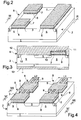
- an integrated device according to a first embodiment of the invention is shown; said integrated device has a stripe structure.
- An N-type epitaxial layer 2 with low dopant concentration is grown on a N-type substrate 1 with high dopant concentration.
- a plurality of body region stripes 3 having P-type dopant are formed inside the epitaxial layer 2.
- the body region stripes 3 are adjacent and parallel to each other and they are alternated with portions 5 of the epitaxial layer 2, as shown in Figure 2.
- a silicon oxide layer 6 is placed and a polysilicon layer 7 is placed over the silicon oxide layer 6 ( Figures 2 and 3); the layers 6 and 7 have a stripe shape and the stripes are parallel to each other and form a plurality of elementary structure of the integrated device.
- the succession of the steps of the integrated device manufacturing process continues with a successive masking and attack step of the polysilicon 7 and of the silicon oxide 6 of at least one elementary structure, that is of at least one polysilicon stripe 7 and of the underlying silicon oxide layer 6, on at least one zone 8.
- the masking and the attack of the polysilicon 7 and of the silicon oxide 6 are made up for forming an interruption of the elementary structure, that is of the polysilicon stripe 7 and of the underlying silicon oxide stripe 6, for the entire width of the stripes.
- the regions 10 with high dopant concentration of N-type are formed and there is a step for the thermal diffusion of the P dopant of the body regions 3 so that they extend partially under the silicon oxide stripes 6 ( Figure 3).
- MOS elementary cells (wherein for MOS elementary cell it is intended the block constituted by two source regions 10, a portion 5 of the epitaxial layer 2 and a gate structure formed by the layers 6 and 7) are formed in the other zones which form the MOS power transistor.
- the metal layers 12 and 13 are respectively the source and drain electrodes of each MOS elementary cell.
- the formation of the channel of said MOS elementary cells occurs in a transversal way with respect to the longitudinal extension of the body stripes 3 and of the elementary structures formed by the stripes 6 and 7.
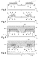
- FIGs 4, 6-9 an integrated device according to a second embodiment of the present invention is shown which differs from the first embodiment because the masking and attack step of the polysilicon 7 and of the silicon oxide 6 of at least one elementary structure, that is of at least one polysilicon stripe 7 and at least one silicon oxide stripe 6, in the zone 8 does not provide the whole removal of the oxide and of the polysilicon in said zone 8.
- an opening 9 for example comprised between 1 ⁇ m and 5 ⁇ m
- the dielectric layer 11 covers the walls of the opening 9 to prevent the contact of the metal 12 with the polysilicon 7.
- the width L2 of the stripes 6 and 7 in the zones 8 is preferably smaller than the typical width L1 of the stripes 6 and 7, as shown in Figure 4; it is defined in base on the breakdown voltage of the integrated device which is not lower than that of the integrated device without Schottky diodes, therefore the width L2 depends on the dopant concentration of the regions 3, on the thickness of the oxide, etc.
- zones 8 in more than one elementary structure are formed; said zones 8 are preferably aligned transversal to each other and are alternated longitudinally to the MOS elementary cells, as shown in Figure 4.
- the only difference consists in that the width L2 of the stripes 6 and 7 of the zones 8 is equal to the typical width L1 of the stripes 6 and 7.
- the integrated device is therefore formed by a MOS power transistor and by a Schottky diode arranged in parallel to the body diode.
- FIG. 10 A part of a multi-drain device according to prior art is shown in Figure 10.
- the integrated device in Figure 10 presents a multi-drain (MD) device structure, that is it presents a formation of P-type region columns under the body regions 300.
- a succession of N-type epitaxial layers 207 with low dopant concentration are formed on a N-type semiconductor substrate 101 with high dopant concentration.
- After the formation of the last epitaxial layer 207 of the succession of epitaxial layers 207 columns 227 of the P-type regions 217 are formed.
- a plurality of stripes of body regions 300 having P-type dopant is formed inside the last epitaxial layer 207; the body region stripes 300 are adjacent and parallel to each other and they are alternated to portions 500 of the last epitaxial layer 207, as shown in Figure 10.
- At least one source region 107 is inside each body stripes 300.
- a silicon oxide layer 60 is placed over the plurality of regions 500 of the last epitaxial layer 207 and a polysilicon layer 70 is placed over the silicon oxide layer 60; the layers 60 and 70 have shape of stripes which are parallel to each other and which form a plurality of elementary structure of the integrated device.
- a stripe shape dielectric layer 311 is placed over the polysilicon layers 70 and a metal layer 80 is deposited over the layers 311, over the body regions 300 and over the source regions 107.
- a Schottky diode cannot be formed by interrupting the body regions 300 of the single elementary cells of the device and by forming an alternation of body regions and portions of the substrate of the device as shown in the device in Figure 1.
- FIG I 1 an integrated device according a third embodiment of the invention is shown where the elements, which are equal to those of the integrated devices according to the preceding embodiments of the invention which are shown in Figures 2-9, have been indicated by the same number references; said integrated device presents a stripe structure.
- the integrated device in Figure 11 shows a multi-drain (MD) device structure, that is it shows a formation of P-type columns under the body regions 3.
- a succession of N-type epitaxial layers 20 with low dopant concentration is formed on a N-type semiconductor substrate 1 with high dopant concentration.
- MD multi-drain
- each epitaxial layer 20 of the succession of epitaxial layers 20 After the formation of each epitaxial layer 20 of the succession of epitaxial layers 20 it occurs the implant of P-type regions 21 inside said epitaxial layer 20, the formation of another epitaxial layer 20 and the diffusion of the P dopant of the regions 21. After the formation of the last epitaxial layer 20 of the succession of epitaxial layers 20 columns 22 of the P-type regions 21 are formed. Typically a portion of epitaxial layer 20 is placed between the substrate 1 and the below of the columns 22 but it is even possible that the below of the columns 22 is directly contacted by the substrate 1.
- a plurality of body region stripes 3 having P-type dopant is formed inside the last epitaxial layer 20; the body region stripes 3 are adjacent and parallel to each other and they are alternated to portions 5 of the last epitaxial layer 20, as shown in Figure 11.
- a silicon oxide layer 6 is placed over the plurality of regions 5 of the last epitaxial layer 20 and a polysilicon layer 7 is placed over the silicon oxide layer 6; the layers 6 and 7 have shape of stripes parallel to each other and they form a plurality of elementary structures of the integrated device.
- the succession of the steps of the integrated device manufacturing process follows with a successive masking and attack step of the polysilicon 7 and of the silicon oxide 6 of at least one elementary structure, that is of at least one polysilicon stripe 7 and of the underlying silicon oxide layer 6, on at least one zone 8.
- the masking and the attack of the polysilicon 7 and of the silicon oxide 6 is made up for forming an interruption of the elementary structure, that is of the polysilicon stripe 7 and of the underlying silicon oxide stripe 6, for the entire width of the stripes.
- the regions 10 with high dopant concentration of N-type are formed and there is a step for the thermal diffusion of the P dopant of the body regions 3 so that they extend partially under the silicon oxide stripes 6.
- Successive steps provide for the formation of a dielectric layer 11 over and around the silicon oxide layers 6 and the polysilicon layers 7, for the deposition of a metal layer and for the formation of a metal layer on the bottom surface of the substrate 1 (which are not shown in Figure 11).
- the metal layer present over the top surface of the device is deposited over the zones 8 for contacting the silicon of the portions 5 of the epitaxial layer 20; in such a way Schottky diodes are formed in the zones 8 of the integrated device the electrodes of which are constituted by the metal layers present over the top and bottom device surfaces.
- MOS elementary cells (wherein for MOS elementary cell it is intended the block constituted by two source regions 10, a portion 5 of the epitaxial layer 2 and a gate structure formed by the layers 6 and 7) are formed in the other zones which form the MOS power transistor.
- the metal layers present over the top and bottom device surfaces are respectively the source and drain electrodes of each MOS elementary cell.
- the formation of the channel of said MOS elementary cells occurs in a transversal way with respect to the longitudinal extension of the body stripes 3 and of the elementary structures formed by the stripes 6 and 7.
- FIGs 12, 14 and 15 an integrated device according to a fourth embodiment of the present invention is shown which differs from the third embodiment because the masking and attack step of the polysilicon 7 and of the silicon oxide 6 of at least one elementary structure, that is of at least one polysilicon stripe 7 and at least one silicon oxide stripe 6, in the zone 8 does not provide the whole removal of the oxide and of the polysilicon in said zone 8.
- an opening 9 (for example comprised between 1 ⁇ m and 5 ⁇ m) in the polysilicon layer 7 and in the underlying silicon oxide layer 6 ( Figures 12 and 14) is formed to allow the contact of the metal layer 12 with the underlying portion 5 of epitaxial layer 20 ( Figure 15); in such a way a formation of Schottky diodes in the zones 8 of the integrated device occurs the electrodes of which are constituted by the metal layers 12 and 13.
- the dielectric layer 11 covers the walls of the opening 9 to prevent the contact of the metal 12 with the polysilicon 7.
- the width L2 of the stripes 6 and 7 in the zones 8 is preferably smaller than the typical width L1 of the stripes 6 and 7, as shown in Figure 12; it is defined on the base of the breakdown voltage of the integrated device which is not lower than that of the integrated device without Schottky diodes, therefore the width L2 depends on the dopant concentration of the regions 3, on the thickness of the oxide, etc.
- zones 8 in more than one elementary structure are formed; said zones 8 are preferably aligned transversal to each other and are alternated longitudinally to the MOS elementary cells, as shown in Figure 12.
- the only difference consists in that the width L2 of the stripes 6 and 7 of the zones 8 is equal to the typical width L1 of the stripes 6 and 7.
- the integrated device is therefore formed by a MOS power transistor and by a Schottky diode arranged in parallel to the body diode.
- the above shown MD integrated device is particularly util for use at high voltage.
Landscapes
- Engineering & Computer Science (AREA)
- Microelectronics & Electronic Packaging (AREA)
- Power Engineering (AREA)
- Physics & Mathematics (AREA)
- Ceramic Engineering (AREA)
- Condensed Matter Physics & Semiconductors (AREA)
- General Physics & Mathematics (AREA)
- Computer Hardware Design (AREA)
- Manufacturing & Machinery (AREA)
- Chemical & Material Sciences (AREA)
- Composite Materials (AREA)
- Electrodes Of Semiconductors (AREA)
Abstract
Description
- The present invention refers to an integrated device with Schottky diode and with MOS transistor and to the related manufacturing process.
- The MOS devices are frequently used as synchronous rectifiers, for example in the bridge circuit configurations of the DC/DC converters. A synchronous rectifier acts like a diode: it is turned on when its equivalent diode has to conduct and it is turned off when the equivalent diode has to cease the conduction. The vertical semiconductor MOS devices have an intrinsic diode, which is formed by the junction between the body region and the drain region and which is called "body diode", that interferes with the operation of the MOS device as a synchronous rectifier. In fact such body diode switches slowly, it has a high conduction voltage and may product electromagnetic radiation emissions in the circuit configurations where the MOS device is inserted.
- For reducing the switching time of the body diode technologies for controlling the life time of the minority carriers are presently used which consist of introducing metal, as gold or platinum, inside the MOS device. Such technologies cause a reduction of the life time of the minority carriers, increase the conduction losses and do not decrease the electromagnetic radiation emissions in the circuit configurations where the MOS device is inserted.
- Another solution used for reducing the switching time of the body diode consists of arranging a Schottky diode, which has equal voltage and a suitable area, in parallel thereto. The Schottky diode has a fast recovery because minority carriers do not exist and has lower conduction voltage values for the different barrier heights. The combination of the body diode in parallel to the Schottky diode provides for an equivalent structure having a short switching time and a lower conduction voltage.
- Discrete component structures are used for the structure made up by the body diode in parallel to the Schottky diode.
- An integrated type structure is disclosed in US 5886383. In such patent there is the device structure shown in Figure 1. A MOS device having a polygonal cell structure is formed together with a Schottky diode in a common silicon substrate of N+-type. A N-type
epitaxial layer 100 is formed on the said silicon substrate which receives a plurality of P-type regions source regions central openings region 100 protrudes, so that ametal layer 220 contacts theregion 100; in such a way the diode Schottky is formed. In the structure in Figure 1 each channel region is covered by a gate oxide on which apolysilicon layer 200 is superimposed. Anotheroxide layer 210 is superimposed on the polysilicon layer for insulating it from themetal layer 220. A drain electrode is applied under thechip 90. - Therefore the Schottky diode in the MOS device in Figure 1 is formed by interrupting the body regions of the single elementary cells of the device, by forming an alternation of body regions and device substrate portions; said substrate portions are contacted by the metal used for contacting the source regions.
- Such solution, even if it is efficacious, gives the problem of the interruption of the body regions in the MOS elementary cells and results unusable in certain cases, as, for example, in MOS devices having multi-drain structures (MD), that is where the body regions extend in depth inside the substrate of the MOS device.
- In view of the art described, it is an object to present invention to provide an integrated device with Schottky diode and MOS transistor which overcomes the aforementioned drawbacks.
- According to the present invention, this object is obtained by means of an integrated device comprising a MOS transistor and a Schottky diode which are formed on a semiconductor substrate of a first conductivity type, said device comprising a plurality of body region stripes of a second conductivity type which are adjacent and parallel to each other, a first metal layer placed over said substrate and a second metal layer placed under said substrate, said device comprising a plurality of elementary structures parallel to each other each one of which comprises first zones provided with a silicon oxide layer placed over a portion of said substrate which is comprised between two adjacent body region stripes, a polysilicon layer superimposed to said silicon oxide layer, a dielectric layer placed over and around the polysilicon layer, some stripes of said plurality of adjacent body region stripes comprising source regions of the first conductivity type which are placed adj acent to said first zones of the elementary structures to form elementary cells of said MOS transistor, said elementary structures and said body regions stripes extending longitudinally in a transversal way to the formation of the channel in said elementary cells of the MOS transistor, said first metal layer contacting said source regions, characterized in that at least one elementary structure of said plurality of elementary structures comprises at least a second zone adapted to allow the direct contact between said first metal layer and the underlying substrate portion arranged between two adjacent body regions stripes to perform the Schottky diode.
- Always according to the present invention it is possible to provide a process for forming an integrated device as defined in
claim 8. - The features and the advantages of the present invention will be made evident by the following detailed description of embodiments thereof, shown as not limiting examples in the annexed drawings, wherein:
- Figure 1 is a cross-section schematic view of a part of a device according to prior art;
- Figure 2 is a perspective schematic view of a part of an integrated device according to a first embodiment of the present invention at one step of its manufacturing process;
- Figure 3 is a section view of the device in Figure 2 according to a line III-III at a successive step of the process for manufacturing the integrated device;
- Figure 4 is a perspective schematic view of a part of an integrated device according to a second embodiment of the present invention at one step of its manufacturing process;
- Figure 5 is a perspective schematic view of a part of an integrated device according to a variant of the second embodiment of the present invention at one step of its manufacturing process;
- Figure 6 is a section view of the device in Figure 4 according to line VI-VI;
- Figure 7 is a section view of the device in Figure 4 according to line VII-VII;
- Figures 8 and 9 are views analogue to those in Figures 6 and 7 but in a successive step of the manufacturing process of the device;
- Figure 10 is a cross-section view of a part of a multi-drain device according to prior art;
- Figure 11 is a perspective schematic view of a part of an integrated device according to a third embodiment of the present invention at one step of its manufacturing process;
- Figure 12 is a perspective schematic view of a part of an integrated device according to a fourth embodiment of the present invention at one step of its manufacturing process;
- Figure 13 is a perspective schematic view of a part of an integrated device according to a variant of the fourth embodiment of the present invention at one step of its manufacturing process;
- Figure 14 is a section view of the device in Figure 12 according to line XIV-XIV;
- Figure 15 is a view analogue to that in Figure 14 but at a successive step of the manufacturing process of the device.
-
- Referring to Figures 2-3 an integrated device according to a first embodiment of the invention is shown; said integrated device has a stripe structure. An N-type
epitaxial layer 2 with low dopant concentration is grown on a N-type substrate 1 with high dopant concentration. A plurality ofbody region stripes 3 having P-type dopant are formed inside theepitaxial layer 2. Thebody region stripes 3 are adjacent and parallel to each other and they are alternated withportions 5 of theepitaxial layer 2, as shown in Figure 2. Over the plurality ofportions 5 of the epitaxial layer 2 asilicon oxide layer 6 is placed and apolysilicon layer 7 is placed over the silicon oxide layer 6 (Figures 2 and 3); thelayers - The succession of the steps of the integrated device manufacturing process continues with a successive masking and attack step of the
polysilicon 7 and of thesilicon oxide 6 of at least one elementary structure, that is of at least onepolysilicon stripe 7 and of the underlyingsilicon oxide layer 6, on at least onezone 8. The masking and the attack of thepolysilicon 7 and of thesilicon oxide 6 are made up for forming an interruption of the elementary structure, that is of thepolysilicon stripe 7 and of the underlyingsilicon oxide stripe 6, for the entire width of the stripes. - At successive steps of the manufacturing process of the integrated device the
regions 10 with high dopant concentration of N-type are formed and there is a step for the thermal diffusion of the P dopant of thebody regions 3 so that they extend partially under the silicon oxide stripes 6 (Figure 3). - Successive steps provide for the formation of a
dielectric layer 11 over and around thesilicon oxide layers 6 and thepolysilicon layers 7, for the deposition of ametal layer 12 and for the formation of ametal layer 13 on the bottom surface of thesubstrate 1. Themetal layer 12 is deposited over thezones 8 for contacting the silicon of theportions 5 of theepitaxial layers 2; in such a way Schottky diodes are formed in thezones 8 of the integrated device the electrodes of which are constituted by themetal layers source regions 10, aportion 5 of theepitaxial layer 2 and a gate structure formed by thelayers 6 and 7) are formed in the other zones which form the MOS power transistor. Themetal layers body stripes 3 and of the elementary structures formed by thestripes - In Figures 4, 6-9 an integrated device according to a second embodiment of the present invention is shown which differs from the first embodiment because the masking and attack step of the
polysilicon 7 and of thesilicon oxide 6 of at least one elementary structure, that is of at least onepolysilicon stripe 7 and at least onesilicon oxide stripe 6, in thezone 8 does not provide the whole removal of the oxide and of the polysilicon insaid zone 8. In fact in thezone 8 an opening 9 (for example comprised between 1µm and 5µm) in thepolysilicon layer 7 and in the underlying silicon oxide layer 6 (Figures 4 and 7) is formed to allow the contact of themetal layer 12 with theunderlying portion 5 of epitaxial layer 2 (Figures 8 and 9). Thedielectric layer 11 covers the walls of the opening 9 to prevent the contact of themetal 12 with thepolysilicon 7. - The width L2 of the
stripes zones 8 is preferably smaller than the typical width L1 of thestripes regions 3, on the thickness of the oxide, etc. With the width L2 smaller than the width L1 (for example if L1=11µm L2 is comprised between 5µm and 8µm), at the thermal diffusion step of the P dopant of thebody regions 3, after forming a suitable implant window, an alignment ofsaid body regions 3 with the portion of thesilicon oxide 6 of thezone 8 occurs so that portions ofepitaxial layer 2 are not between thebody regions 3 and the beginning of thelayer 6, as shown in Figure 7. - Preferably
different zones 8 in more than one elementary structure are formed; saidzones 8 are preferably aligned transversal to each other and are alternated longitudinally to the MOS elementary cells, as shown in Figure 4. - In the variant of the second embodiment shown in Figure 5 the only difference consists in that the width L2 of the
stripes zones 8 is equal to the typical width L1 of thestripes - The integrated device is therefore formed by a MOS power transistor and by a Schottky diode arranged in parallel to the body diode.
- A part of a multi-drain device according to prior art is shown in Figure 10. The integrated device in Figure 10 presents a multi-drain (MD) device structure, that is it presents a formation of P-type region columns under the
body regions 300. A succession of N-typeepitaxial layers 207 with low dopant concentration are formed on a N-type semiconductor substrate 101 with high dopant concentration. After the formation of eachepitaxial layer 207 of the succession ofepitaxial layers 207 it occurs the implant of P-type regions 217 inside saidepitaxial layer 207, the formation of anotherepitaxial layer 207 and the diffusion of the P dopant of theregions 217. After the formation of the lastepitaxial layer 207 of the succession ofepitaxial layers 207columns 227 of the P-type regions 217 are formed. - A plurality of stripes of
body regions 300 having P-type dopant is formed inside the lastepitaxial layer 207; thebody region stripes 300 are adjacent and parallel to each other and they are alternated toportions 500 of the lastepitaxial layer 207, as shown in Figure 10. At least onesource region 107 is inside eachbody stripes 300. Asilicon oxide layer 60 is placed over the plurality ofregions 500 of thelast epitaxial layer 207 and apolysilicon layer 70 is placed over thesilicon oxide layer 60; thelayers shape dielectric layer 311 is placed over the polysilicon layers 70 and ametal layer 80 is deposited over thelayers 311, over thebody regions 300 and over thesource regions 107. - In the device in Figure 10 a Schottky diode cannot be formed by interrupting the
body regions 300 of the single elementary cells of the device and by forming an alternation of body regions and portions of the substrate of the device as shown in the device in Figure 1. - In Figure I 1 an integrated device according a third embodiment of the invention is shown where the elements, which are equal to those of the integrated devices according to the preceding embodiments of the invention which are shown in Figures 2-9, have been indicated by the same number references; said integrated device presents a stripe structure. In different way from the integrated devices of the preceding embodiments of the invention the integrated device in Figure 11 shows a multi-drain (MD) device structure, that is it shows a formation of P-type columns under the
body regions 3. A succession of N-type epitaxial layers 20 with low dopant concentration is formed on a N-type semiconductor substrate 1 with high dopant concentration. After the formation of eachepitaxial layer 20 of the succession ofepitaxial layers 20 it occurs the implant of P-type regions 21 inside saidepitaxial layer 20, the formation of anotherepitaxial layer 20 and the diffusion of the P dopant of theregions 21. After the formation of thelast epitaxial layer 20 of the succession ofepitaxial layers 20columns 22 of the P-type regions 21 are formed. Typically a portion ofepitaxial layer 20 is placed between thesubstrate 1 and the below of thecolumns 22 but it is even possible that the below of thecolumns 22 is directly contacted by thesubstrate 1. - A plurality of
body region stripes 3 having P-type dopant is formed inside thelast epitaxial layer 20; thebody region stripes 3 are adjacent and parallel to each other and they are alternated toportions 5 of thelast epitaxial layer 20, as shown in Figure 11. Asilicon oxide layer 6 is placed over the plurality ofregions 5 of thelast epitaxial layer 20 and apolysilicon layer 7 is placed over thesilicon oxide layer 6; thelayers - The succession of the steps of the integrated device manufacturing process follows with a successive masking and attack step of the
polysilicon 7 and of thesilicon oxide 6 of at least one elementary structure, that is of at least onepolysilicon stripe 7 and of the underlyingsilicon oxide layer 6, on at least onezone 8. The masking and the attack of thepolysilicon 7 and of thesilicon oxide 6 is made up for forming an interruption of the elementary structure, that is of thepolysilicon stripe 7 and of the underlyingsilicon oxide stripe 6, for the entire width of the stripes. - At successive steps of the manufacturing process of the integrated device the
regions 10 with high dopant concentration of N-type are formed and there is a step for the thermal diffusion of the P dopant of thebody regions 3 so that they extend partially under thesilicon oxide stripes 6. - Successive steps provide for the formation of a
dielectric layer 11 over and around thesilicon oxide layers 6 and the polysilicon layers 7, for the deposition of a metal layer and for the formation of a metal layer on the bottom surface of the substrate 1 (which are not shown in Figure 11). The metal layer present over the top surface of the device is deposited over thezones 8 for contacting the silicon of theportions 5 of theepitaxial layer 20; in such a way Schottky diodes are formed in thezones 8 of the integrated device the electrodes of which are constituted by the metal layers present over the top and bottom device surfaces. MOS elementary cells (wherein for MOS elementary cell it is intended the block constituted by twosource regions 10, aportion 5 of theepitaxial layer 2 and a gate structure formed by thelayers 6 and 7) are formed in the other zones which form the MOS power transistor. The metal layers present over the top and bottom device surfaces are respectively the source and drain electrodes of each MOS elementary cell. The formation of the channel of said MOS elementary cells occurs in a transversal way with respect to the longitudinal extension of thebody stripes 3 and of the elementary structures formed by thestripes - In Figures 12, 14 and 15 an integrated device according to a fourth embodiment of the present invention is shown which differs from the third embodiment because the masking and attack step of the
polysilicon 7 and of thesilicon oxide 6 of at least one elementary structure, that is of at least onepolysilicon stripe 7 and at least onesilicon oxide stripe 6, in thezone 8 does not provide the whole removal of the oxide and of the polysilicon in saidzone 8. In fact in thezone 8 an opening 9 (for example comprised between 1µm and 5µm) in thepolysilicon layer 7 and in the underlying silicon oxide layer 6 (Figures 12 and 14) is formed to allow the contact of themetal layer 12 with theunderlying portion 5 of epitaxial layer 20 (Figure 15); in such a way a formation of Schottky diodes in thezones 8 of the integrated device occurs the electrodes of which are constituted by the metal layers 12 and 13. Thedielectric layer 11 covers the walls of theopening 9 to prevent the contact of themetal 12 with thepolysilicon 7. - The width L2 of the
stripes zones 8 is preferably smaller than the typical width L1 of thestripes regions 3, on the thickness of the oxide, etc. With the width L2 smaller than the width L1 (for example if L1=11µm L2 is comprised between 5µm and 8µm), at the thermal diffusion step of the P dopant of thebody regions 3, after forming a suitable implant window, an alignment of saidbody regions 3 with the portion of thesilicon oxide 6 of thezone 8 occurs so that portions ofepitaxial layer 2 are not between thebody regions 3 and the beginning of thelayer 6, as shown in Figure 14. - Preferably
different zones 8 in more than one elementary structure are formed; saidzones 8 are preferably aligned transversal to each other and are alternated longitudinally to the MOS elementary cells, as shown in Figure 12. - In the variant of the fourth embodiment shown in Figure 13 the only difference consists in that the width L2 of the
stripes zones 8 is equal to the typical width L1 of thestripes - The integrated device is therefore formed by a MOS power transistor and by a Schottky diode arranged in parallel to the body diode.
- The above shown MD integrated device is particularly util for use at high voltage.
Claims (14)
- Integrated device comprising a MOS transistor and a Schottky diode which are formed on a semiconductor substrate (1, 2; 1, 20) of a first conductivity type, said device comprising a plurality of body region stripes (3) of a second conductivity type which are adjacent and parallel to each other, a first metal layer (12) placed over said substrate (1, 2; 1, 20) and a second metal layer placed under said substrate (1, 2; 1, 20), said device comprising a plurality of elementary structures (6, 7) parallel to each other each one of which comprises first zones provided with a silicon oxide layer (6) placed over a portion of said substrate which is comprised between two adjacent body region stripes (3), a polysilicon layer (7) superimposed to said silicon oxide layer (6), a dielectric layer (11) placed over and around the polysilicon layer (7), some stripes (3) of said plurality of adjacent body region stripes (3) comprising source regions (10) of the first conductivity type which are placed adjacent to said first zones of the elementary structures (6, 7) to form elementary cells of said MOS transistor, said elementary structures (6, 7) and said body regions stripes (3) extending longitudinally in a transversal way to the formation of the channel in said elementary cells of the MOS transistor, said first metal layer (12) contacting said source regions (10), characterized in that at least one elementary structure (6, 7) of said plurality of elementary structures (6, 7) comprises at least a second zone (8) adapted to allow the direct contact between said first metal layer (12) and the underlying substrate portion (5) arranged between two adjacent body regions stripes (3) to perform the Schottky diode.
- Integrated device according to claim 1, characterized in that said at least a second zone (8) comprises a further silicon oxide layer (6) placed over said substrate portion (5), a further polysilicon layer (7) superimposed to said silicon oxide layer (6), a further dielectric layer (11) placed over and around the polysilicon layer (7) and a cavity (9) formed in the further dielectric layer (11), in the further polysilicon layer (7) and in the further silicon oxide layer (6) and it being adapted to be filled up with said first metal layer (12) for contacting said substrate portion (5), the walls of said cavity (9) being covered with dielectric.
- Integrated device according to claim 1 or 2, characterized in that said substrate (1, 20) comprises a plurality of epitaxial layers (20) of the first conductivityt type, each one of said epitaxial layers (20) comprising further regions (21) of the second conductivity type for forming columns (22) of said further regions (21) of the second conductivity type under and in contact with said body region stripes (3).
- Integrated device according to claim 3, characterized in that said substrate (1, 2; 1, 20) comprises a layer (1) of the first conductivity type with high dopant concentration with which said columns (22) are in contact.
- Integrated device according to claim 3, characterized in that said substrate (1, 2; 1, 20) comprises a layer (1) of the first conductivity type with high dopant concentration, a portion of a layer of said plurality of epitaxial layers (20) of the first conductivity type being arranged between said columns (22) and said layer (1) of the first conductivity type with high dopant concentration.
- Integrated device according to anyone of the preceding claims, characterized in that said first conductivity type is of N-type.
- Integrated device according to anyone of the preceding claims, characterized in that said first conductivity type is of P-type.
- Manufacturing process of an integrated device comprising a MOS transistor and a Schottky diode, said process comprising a first step of forming a plurality of body region stripes (3) of a first conductivity type inside a semiconductor material substrate (1, 2; 1, 20) of a second conductivity type, said body region stripes (3) being adjacent and parallel to each other, a second step of forming a plurality of elementary structures (6, 7) parallel to each other each one of which comprises a silicon oxide layer (6) placed over a portion (5) of said substrate which is comprised between two adjacent body region stripes (3), a polysilicon layer (7) superimposed to said silicon oxide layer (6), a third step of forming source regions (10) of the second conductivity type inside some stripes (3) of said plurality of adjacent body region stripes (3) and in a adjacent way to a first zones of said elementary structures (6, 7) for forming elementary cells of said MOS transistor, said elementary structures (6, 7) and said body regions stripes (3) extending longitudinally in a transversal way to the formation of the channel in said elementary cells of the MOS transistor, a fourth step for depositing a dielectric layer (11) over and around said elementary structures (6, 7), a fifth step for depositing a first metal layer (12) over said substrate for contacting the source regions (10), a sixt step for forming a second metal layer (13) under said substrate (1, 2; 1, 20), characterized by comprising between said second step and said third step a further step of masking and attack of the silicon oxide layer (6) and of the superimposed polysilicon layer (7) of at least one elementary structure (6, 7) in at least a second zone (8) of said elementary structure (6, 7), said first metal layer (12) being deposited at said fifth step for contacting the underlying substrate portion (5) of said at least a second zone (8) to perform the Schottky diode.
- Process according to claim 8, characterized in that at said further step a cavity (9) is formed in the dielectric layer (11), in the polysilicon layer (7) and in the silicon oxide layer (6), said cavity (9) being filled up with said first metal layer (12) for contacting said substrate portion (5) at said fifth step, the walls of said cavity (9) being covered with dielectric of said dielectric layer (11) deposited in said fourth step.
- Process according to claim 8 or 9, characterized in that in said first step of forming of the body regions stripes (3) a plurality of sub-steps occurs which comprise a plurality of first sub-steps of forming a plurality of epitaxial layers (20) of the second conductivity type inside said substrate (1, 20), said first sub-steps being alternated to a plurality of second sub-steps of forming further regions (21) of the first conductivity type inside said epitaxial layers (20) for forming columns (22) of said further regions (21) of the first conductivity type under and in contact with said body region stripes (3).
- Process according to claim 10, characterized in that said substrate (1, 2; 1, 20) comprises a layer (1) of the second conductivity type with high dopant concentration with which said columns (22) are in contact.
- Process according to claim 10, characterized in that said substrate (1, 2; 1, 20) comprises a layer (1) of the second conductivity type with high dopant concentration, a portion of a layer of said plurality of epitaxial layers (20) of the second conductivity type being arranged between said columns (22) and said layer (1) of the second conductivity type with high dopant concentration.
- Process according to anyone of the claims from 8 to 12, characterized in that said first conductivity type is of N-type.
- Process according to anyone of the claims from 8 to 12, characterized in that said first conductivity type is of P-type.
Applications Claiming Priority (2)
| Application Number | Priority Date | Filing Date | Title |
|---|---|---|---|
| IT002700A ITMI20022700A1 (en) | 2002-12-20 | 2002-12-20 | INTEGRATED DEVICE WITH SCHOTTKY DIODE AND MOS TRANSITOR |
| ITMI20022700 | 2002-12-20 |
Publications (3)
| Publication Number | Publication Date |
|---|---|
| EP1432037A2 true EP1432037A2 (en) | 2004-06-23 |
| EP1432037A3 EP1432037A3 (en) | 2005-06-22 |
| EP1432037B1 EP1432037B1 (en) | 2008-12-03 |
Family
ID=32375552
Family Applications (1)
| Application Number | Title | Priority Date | Filing Date |
|---|---|---|---|
| EP03079092A Expired - Lifetime EP1432037B1 (en) | 2002-12-20 | 2003-12-16 | Integrated device with Schottky diode and with MOS transistor and related manufacturing process |
Country Status (4)
| Country | Link |
|---|---|
| US (2) | US6841836B2 (en) |
| EP (1) | EP1432037B1 (en) |
| DE (1) | DE60325008D1 (en) |
| IT (1) | ITMI20022700A1 (en) |
Cited By (1)
| Publication number | Priority date | Publication date | Assignee | Title |
|---|---|---|---|---|
| EP3425676A1 (en) | 2017-07-05 | 2019-01-09 | STMicroelectronics S.r.l. | Mosfet device of silicon carbide having an integrated diode and manufacturing process thereof |
Families Citing this family (10)
| Publication number | Priority date | Publication date | Assignee | Title |
|---|---|---|---|---|
| US7667264B2 (en) * | 2004-09-27 | 2010-02-23 | Alpha And Omega Semiconductor Limited | Shallow source MOSFET |
| US7285822B2 (en) * | 2005-02-11 | 2007-10-23 | Alpha & Omega Semiconductor, Inc. | Power MOS device |
| US8093651B2 (en) * | 2005-02-11 | 2012-01-10 | Alpha & Omega Semiconductor Limited | MOS device with integrated schottky diode in active region contact trench |
| US8362547B2 (en) | 2005-02-11 | 2013-01-29 | Alpha & Omega Semiconductor Limited | MOS device with Schottky barrier controlling layer |
| US7948029B2 (en) | 2005-02-11 | 2011-05-24 | Alpha And Omega Semiconductor Incorporated | MOS device with varying trench depth |
| US8283723B2 (en) * | 2005-02-11 | 2012-10-09 | Alpha & Omega Semiconductor Limited | MOS device with low injection diode |
| US7227207B2 (en) * | 2005-03-03 | 2007-06-05 | International Business Machines Corporation | Dense semiconductor fuse array |
| US8933506B2 (en) * | 2011-01-31 | 2015-01-13 | Alpha And Omega Semiconductor Incorporated | Diode structures with controlled injection efficiency for fast switching |
| JP6104743B2 (en) * | 2013-07-18 | 2017-03-29 | 株式会社豊田中央研究所 | FET with built-in Schottky diode |
| WO2018063191A1 (en) * | 2016-09-28 | 2018-04-05 | Intel Corporation | Techniques for forming schottky diodes on semipolar planes of group iii-n material structures |
Citations (4)
| Publication number | Priority date | Publication date | Assignee | Title |
|---|---|---|---|---|
| EP0975024A2 (en) * | 1998-07-24 | 2000-01-26 | Fuji Electric Co. Ltd. | Semiconductor device with alternating conductivity type layer and method of manufacturing the same |
| DE10008545A1 (en) * | 2000-02-24 | 2001-08-30 | Bosch Gmbh Robert | Monolithic integrated semiconducting component has first region with additional contact to higher concentration region so Ohmic contact exists and is connected to Schottky diode(s) |
| EP1198011A1 (en) * | 1999-07-15 | 2002-04-17 | Rohm Co., Ltd. | Semiconductor device including mos field-effect transistor |
| EP1204145A2 (en) * | 2000-10-23 | 2002-05-08 | Matsushita Electric Industrial Co., Ltd. | Semiconductor element |
Family Cites Families (10)
| Publication number | Priority date | Publication date | Assignee | Title |
|---|---|---|---|---|
| GB1140841A (en) * | 1965-01-24 | 1969-01-22 | Production Engineering Res Ass | Improved cutting tool |
| US4729697A (en) * | 1986-06-18 | 1988-03-08 | Dijet Inc. | Milling cutter |
| US5556239A (en) * | 1993-10-18 | 1996-09-17 | Valenite Inc. | Positive cutting insert with compound clearance faces |
| US5639189A (en) * | 1994-11-08 | 1997-06-17 | Ingersoll Cutting Tool Company | Plunge milling insert |
| US6049108A (en) * | 1995-06-02 | 2000-04-11 | Siliconix Incorporated | Trench-gated MOSFET with bidirectional voltage clamping |
| US5853267A (en) * | 1996-08-22 | 1998-12-29 | Iscar Ltd. | Cutting insert |
| US5886383A (en) | 1997-01-10 | 1999-03-23 | International Rectifier Corporation | Integrated schottky diode and mosgated device |
| US5956578A (en) * | 1997-04-23 | 1999-09-21 | Motorola, Inc. | Method of fabricating vertical FET with Schottky diode |
| SE512736C2 (en) * | 1997-06-10 | 2000-05-08 | Seco Tools Ab | Face Milling Tools |
| DE19848045C2 (en) * | 1998-10-17 | 2002-01-31 | Fette Wilhelm Gmbh | Insert milling cutters |
-
2002
- 2002-12-20 IT IT002700A patent/ITMI20022700A1/en unknown
-
2003
- 2003-12-16 DE DE60325008T patent/DE60325008D1/en not_active Expired - Lifetime
- 2003-12-16 EP EP03079092A patent/EP1432037B1/en not_active Expired - Lifetime
- 2003-12-16 US US10/738,952 patent/US6841836B2/en not_active Expired - Lifetime
-
2004
- 2004-12-28 US US11/023,957 patent/US7071062B2/en not_active Expired - Lifetime
Patent Citations (4)
| Publication number | Priority date | Publication date | Assignee | Title |
|---|---|---|---|---|
| EP0975024A2 (en) * | 1998-07-24 | 2000-01-26 | Fuji Electric Co. Ltd. | Semiconductor device with alternating conductivity type layer and method of manufacturing the same |
| EP1198011A1 (en) * | 1999-07-15 | 2002-04-17 | Rohm Co., Ltd. | Semiconductor device including mos field-effect transistor |
| DE10008545A1 (en) * | 2000-02-24 | 2001-08-30 | Bosch Gmbh Robert | Monolithic integrated semiconducting component has first region with additional contact to higher concentration region so Ohmic contact exists and is connected to Schottky diode(s) |
| EP1204145A2 (en) * | 2000-10-23 | 2002-05-08 | Matsushita Electric Industrial Co., Ltd. | Semiconductor element |
Cited By (1)
| Publication number | Priority date | Publication date | Assignee | Title |
|---|---|---|---|---|
| EP3425676A1 (en) | 2017-07-05 | 2019-01-09 | STMicroelectronics S.r.l. | Mosfet device of silicon carbide having an integrated diode and manufacturing process thereof |
Also Published As
| Publication number | Publication date |
|---|---|
| US7071062B2 (en) | 2006-07-04 |
| EP1432037A3 (en) | 2005-06-22 |
| ITMI20022700A1 (en) | 2004-06-21 |
| DE60325008D1 (en) | 2009-01-15 |
| EP1432037B1 (en) | 2008-12-03 |
| US20050118766A1 (en) | 2005-06-02 |
| US6841836B2 (en) | 2005-01-11 |
| US20040140512A1 (en) | 2004-07-22 |
Similar Documents
| Publication | Publication Date | Title |
|---|---|---|
| US8222693B2 (en) | Trench-gate transistors and their manufacture | |
| US6541820B1 (en) | Low voltage planar power MOSFET with serpentine gate pattern | |
| EP1323191B1 (en) | Method for manufacturing a trench dmos transistor with embedded trench schottky rectifier | |
| US7052963B2 (en) | Method of forming trench transistor with chained implanted body including a plurality of implantation with different energies | |
| US6476443B1 (en) | MOSgated device with trench structure and remote contact and process for its manufacture | |
| EP1188189B1 (en) | Trenched schottky rectifiers | |
| EP1415334B1 (en) | Manufacture of semiconductor devices with schottky barriers | |
| EP1145326B1 (en) | Cellular trench-gate field-effect transistors | |
| US6979865B2 (en) | Cellular mosfet devices and their manufacture | |
| US20060017100A1 (en) | Dynamic deep depletion field effect transistor | |
| US6787872B2 (en) | Lateral conduction superjunction semiconductor device | |
| US9287354B2 (en) | Semiconductor component and method for producing it | |
| US20010020720A1 (en) | Field-effect semiconductor devices | |
| US7102182B2 (en) | Semiconductor device | |
| EP1432037B1 (en) | Integrated device with Schottky diode and with MOS transistor and related manufacturing process | |
| US6552363B2 (en) | Polysilicon FET built on silicon carbide diode substrate | |
| KR100214408B1 (en) | Termination structure of semiconductor device and process for manufacture thereof | |
| US8004049B2 (en) | Power semiconductor device | |
| EP0961325B1 (en) | High integration density MOS technology power device | |
| EP1500144B1 (en) | Trench-gate semiconductor devices | |
| US6452219B1 (en) | Insulated gate bipolar transistor and method of fabricating the same | |
| CN118116927A (en) | SiC JBSFET layout structure capable of saving area |
Legal Events
| Date | Code | Title | Description |
|---|---|---|---|
| PUAI | Public reference made under article 153(3) epc to a published international application that has entered the european phase |
Free format text: ORIGINAL CODE: 0009012 |
|
| AK | Designated contracting states |
Kind code of ref document: A2 Designated state(s): AT BE BG CH CY CZ DE DK EE ES FI FR GB GR HU IE IT LI LU MC NL PT RO SE SI SK TR |
|
| AX | Request for extension of the european patent |
Extension state: AL LT LV MK |
|
| PUAL | Search report despatched |
Free format text: ORIGINAL CODE: 0009013 |
|
| AK | Designated contracting states |
Kind code of ref document: A3 Designated state(s): AT BE BG CH CY CZ DE DK EE ES FI FR GB GR HU IE IT LI LU MC NL PT RO SE SI SK TR |
|
| AX | Request for extension of the european patent |
Extension state: AL LT LV MK |
|
| 17P | Request for examination filed |
Effective date: 20051213 |
|
| AKX | Designation fees paid |
Designated state(s): DE FR GB IT |
|
| 17Q | First examination report despatched |
Effective date: 20061005 |
|
| 17Q | First examination report despatched |
Effective date: 20061005 |
|
| GRAP | Despatch of communication of intention to grant a patent |
Free format text: ORIGINAL CODE: EPIDOSNIGR1 |
|
| GRAS | Grant fee paid |
Free format text: ORIGINAL CODE: EPIDOSNIGR3 |
|
| GRAA | (expected) grant |
Free format text: ORIGINAL CODE: 0009210 |
|
| AK | Designated contracting states |
Kind code of ref document: B1 Designated state(s): DE FR GB IT |
|
| REG | Reference to a national code |
Ref country code: GB Ref legal event code: FG4D |
|
| REF | Corresponds to: |
Ref document number: 60325008 Country of ref document: DE Date of ref document: 20090115 Kind code of ref document: P |
|
| PLBE | No opposition filed within time limit |
Free format text: ORIGINAL CODE: 0009261 |
|
| STAA | Information on the status of an ep patent application or granted ep patent |
Free format text: STATUS: NO OPPOSITION FILED WITHIN TIME LIMIT |
|
| 26N | No opposition filed |
Effective date: 20090904 |
|
| GBPC | Gb: european patent ceased through non-payment of renewal fee |
Effective date: 20090303 |
|
| PG25 | Lapsed in a contracting state [announced via postgrant information from national office to epo] |
Ref country code: FR Free format text: LAPSE BECAUSE OF NON-PAYMENT OF DUE FEES Effective date: 20090203 Ref country code: GB Free format text: LAPSE BECAUSE OF NON-PAYMENT OF DUE FEES Effective date: 20090303 |
|
| PGFP | Annual fee paid to national office [announced via postgrant information from national office to epo] |
Ref country code: IT Payment date: 20101127 Year of fee payment: 8 |
|
| REG | Reference to a national code |
Ref country code: FR Ref legal event code: ST Effective date: 20111202 |
|
| PG25 | Lapsed in a contracting state [announced via postgrant information from national office to epo] |
Ref country code: IT Free format text: LAPSE BECAUSE OF NON-PAYMENT OF DUE FEES Effective date: 20121216 |
|
| REG | Reference to a national code |
Ref country code: DE Ref legal event code: R082 Ref document number: 60325008 Country of ref document: DE Representative=s name: SCHMITT-NILSON SCHRAUD WAIBEL WOHLFROM PATENTA, DE |
|
| PGFP | Annual fee paid to national office [announced via postgrant information from national office to epo] |
Ref country code: DE Payment date: 20221122 Year of fee payment: 20 |
|
| REG | Reference to a national code |
Ref country code: DE Ref legal event code: R071 Ref document number: 60325008 Country of ref document: DE |