EP3425449A2 - Anzeigevorrichtung - Google Patents
Anzeigevorrichtung Download PDFInfo
- Publication number
- EP3425449A2 EP3425449A2 EP18173671.1A EP18173671A EP3425449A2 EP 3425449 A2 EP3425449 A2 EP 3425449A2 EP 18173671 A EP18173671 A EP 18173671A EP 3425449 A2 EP3425449 A2 EP 3425449A2
- Authority
- EP
- European Patent Office
- Prior art keywords
- liquid crystal
- substrate
- display device
- layer
- light control
- Prior art date
- Legal status (The legal status is an assumption and is not a legal conclusion. Google has not performed a legal analysis and makes no representation as to the accuracy of the status listed.)
- Granted
Links
Images







Classifications
-
- G—PHYSICS
- G02—OPTICS
- G02F—OPTICAL DEVICES OR ARRANGEMENTS FOR THE CONTROL OF LIGHT BY MODIFICATION OF THE OPTICAL PROPERTIES OF THE MEDIA OF THE ELEMENTS INVOLVED THEREIN; NON-LINEAR OPTICS; FREQUENCY-CHANGING OF LIGHT; OPTICAL LOGIC ELEMENTS; OPTICAL ANALOGUE/DIGITAL CONVERTERS
- G02F1/00—Devices or arrangements for the control of the intensity, colour, phase, polarisation or direction of light arriving from an independent light source, e.g. switching, gating or modulating; Non-linear optics
- G02F1/01—Devices or arrangements for the control of the intensity, colour, phase, polarisation or direction of light arriving from an independent light source, e.g. switching, gating or modulating; Non-linear optics for the control of the intensity, phase, polarisation or colour
- G02F1/13—Devices or arrangements for the control of the intensity, colour, phase, polarisation or direction of light arriving from an independent light source, e.g. switching, gating or modulating; Non-linear optics for the control of the intensity, phase, polarisation or colour based on liquid crystals, e.g. single liquid crystal display cells
- G02F1/133—Constructional arrangements; Operation of liquid crystal cells; Circuit arrangements
- G02F1/1333—Constructional arrangements; Manufacturing methods
- G02F1/1335—Structural association of cells with optical devices, e.g. polarisers or reflectors
- G02F1/133504—Diffusing, scattering, diffracting elements
-
- G—PHYSICS
- G02—OPTICS
- G02F—OPTICAL DEVICES OR ARRANGEMENTS FOR THE CONTROL OF LIGHT BY MODIFICATION OF THE OPTICAL PROPERTIES OF THE MEDIA OF THE ELEMENTS INVOLVED THEREIN; NON-LINEAR OPTICS; FREQUENCY-CHANGING OF LIGHT; OPTICAL LOGIC ELEMENTS; OPTICAL ANALOGUE/DIGITAL CONVERTERS
- G02F1/00—Devices or arrangements for the control of the intensity, colour, phase, polarisation or direction of light arriving from an independent light source, e.g. switching, gating or modulating; Non-linear optics
- G02F1/01—Devices or arrangements for the control of the intensity, colour, phase, polarisation or direction of light arriving from an independent light source, e.g. switching, gating or modulating; Non-linear optics for the control of the intensity, phase, polarisation or colour
- G02F1/13—Devices or arrangements for the control of the intensity, colour, phase, polarisation or direction of light arriving from an independent light source, e.g. switching, gating or modulating; Non-linear optics for the control of the intensity, phase, polarisation or colour based on liquid crystals, e.g. single liquid crystal display cells
- G02F1/133—Constructional arrangements; Operation of liquid crystal cells; Circuit arrangements
- G02F1/1333—Constructional arrangements; Manufacturing methods
- G02F1/1335—Structural association of cells with optical devices, e.g. polarisers or reflectors
- G02F1/133528—Polarisers
-
- G—PHYSICS
- G02—OPTICS
- G02F—OPTICAL DEVICES OR ARRANGEMENTS FOR THE CONTROL OF LIGHT BY MODIFICATION OF THE OPTICAL PROPERTIES OF THE MEDIA OF THE ELEMENTS INVOLVED THEREIN; NON-LINEAR OPTICS; FREQUENCY-CHANGING OF LIGHT; OPTICAL LOGIC ELEMENTS; OPTICAL ANALOGUE/DIGITAL CONVERTERS
- G02F1/00—Devices or arrangements for the control of the intensity, colour, phase, polarisation or direction of light arriving from an independent light source, e.g. switching, gating or modulating; Non-linear optics
- G02F1/01—Devices or arrangements for the control of the intensity, colour, phase, polarisation or direction of light arriving from an independent light source, e.g. switching, gating or modulating; Non-linear optics for the control of the intensity, phase, polarisation or colour
- G02F1/13—Devices or arrangements for the control of the intensity, colour, phase, polarisation or direction of light arriving from an independent light source, e.g. switching, gating or modulating; Non-linear optics for the control of the intensity, phase, polarisation or colour based on liquid crystals, e.g. single liquid crystal display cells
- G02F1/133—Constructional arrangements; Operation of liquid crystal cells; Circuit arrangements
- G02F1/1333—Constructional arrangements; Manufacturing methods
- G02F1/1335—Structural association of cells with optical devices, e.g. polarisers or reflectors
- G02F1/133509—Filters, e.g. light shielding masks
-
- G—PHYSICS
- G02—OPTICS
- G02F—OPTICAL DEVICES OR ARRANGEMENTS FOR THE CONTROL OF LIGHT BY MODIFICATION OF THE OPTICAL PROPERTIES OF THE MEDIA OF THE ELEMENTS INVOLVED THEREIN; NON-LINEAR OPTICS; FREQUENCY-CHANGING OF LIGHT; OPTICAL LOGIC ELEMENTS; OPTICAL ANALOGUE/DIGITAL CONVERTERS
- G02F1/00—Devices or arrangements for the control of the intensity, colour, phase, polarisation or direction of light arriving from an independent light source, e.g. switching, gating or modulating; Non-linear optics
- G02F1/01—Devices or arrangements for the control of the intensity, colour, phase, polarisation or direction of light arriving from an independent light source, e.g. switching, gating or modulating; Non-linear optics for the control of the intensity, phase, polarisation or colour
- G02F1/13—Devices or arrangements for the control of the intensity, colour, phase, polarisation or direction of light arriving from an independent light source, e.g. switching, gating or modulating; Non-linear optics for the control of the intensity, phase, polarisation or colour based on liquid crystals, e.g. single liquid crystal display cells
- G02F1/133—Constructional arrangements; Operation of liquid crystal cells; Circuit arrangements
- G02F1/1333—Constructional arrangements; Manufacturing methods
- G02F1/1335—Structural association of cells with optical devices, e.g. polarisers or reflectors
- G02F1/133509—Filters, e.g. light shielding masks
- G02F1/133514—Colour filters
-
- G—PHYSICS
- G02—OPTICS
- G02F—OPTICAL DEVICES OR ARRANGEMENTS FOR THE CONTROL OF LIGHT BY MODIFICATION OF THE OPTICAL PROPERTIES OF THE MEDIA OF THE ELEMENTS INVOLVED THEREIN; NON-LINEAR OPTICS; FREQUENCY-CHANGING OF LIGHT; OPTICAL LOGIC ELEMENTS; OPTICAL ANALOGUE/DIGITAL CONVERTERS
- G02F1/00—Devices or arrangements for the control of the intensity, colour, phase, polarisation or direction of light arriving from an independent light source, e.g. switching, gating or modulating; Non-linear optics
- G02F1/01—Devices or arrangements for the control of the intensity, colour, phase, polarisation or direction of light arriving from an independent light source, e.g. switching, gating or modulating; Non-linear optics for the control of the intensity, phase, polarisation or colour
- G02F1/13—Devices or arrangements for the control of the intensity, colour, phase, polarisation or direction of light arriving from an independent light source, e.g. switching, gating or modulating; Non-linear optics for the control of the intensity, phase, polarisation or colour based on liquid crystals, e.g. single liquid crystal display cells
- G02F1/133—Constructional arrangements; Operation of liquid crystal cells; Circuit arrangements
- G02F1/1333—Constructional arrangements; Manufacturing methods
- G02F1/1335—Structural association of cells with optical devices, e.g. polarisers or reflectors
- G02F1/133524—Light-guides, e.g. fibre-optic bundles, louvered or jalousie light-guides
-
- G—PHYSICS
- G02—OPTICS
- G02F—OPTICAL DEVICES OR ARRANGEMENTS FOR THE CONTROL OF LIGHT BY MODIFICATION OF THE OPTICAL PROPERTIES OF THE MEDIA OF THE ELEMENTS INVOLVED THEREIN; NON-LINEAR OPTICS; FREQUENCY-CHANGING OF LIGHT; OPTICAL LOGIC ELEMENTS; OPTICAL ANALOGUE/DIGITAL CONVERTERS
- G02F1/00—Devices or arrangements for the control of the intensity, colour, phase, polarisation or direction of light arriving from an independent light source, e.g. switching, gating or modulating; Non-linear optics
- G02F1/01—Devices or arrangements for the control of the intensity, colour, phase, polarisation or direction of light arriving from an independent light source, e.g. switching, gating or modulating; Non-linear optics for the control of the intensity, phase, polarisation or colour
- G02F1/13—Devices or arrangements for the control of the intensity, colour, phase, polarisation or direction of light arriving from an independent light source, e.g. switching, gating or modulating; Non-linear optics for the control of the intensity, phase, polarisation or colour based on liquid crystals, e.g. single liquid crystal display cells
- G02F1/133—Constructional arrangements; Operation of liquid crystal cells; Circuit arrangements
- G02F1/1333—Constructional arrangements; Manufacturing methods
- G02F1/1335—Structural association of cells with optical devices, e.g. polarisers or reflectors
- G02F1/133553—Reflecting elements
-
- G—PHYSICS
- G02—OPTICS
- G02F—OPTICAL DEVICES OR ARRANGEMENTS FOR THE CONTROL OF LIGHT BY MODIFICATION OF THE OPTICAL PROPERTIES OF THE MEDIA OF THE ELEMENTS INVOLVED THEREIN; NON-LINEAR OPTICS; FREQUENCY-CHANGING OF LIGHT; OPTICAL LOGIC ELEMENTS; OPTICAL ANALOGUE/DIGITAL CONVERTERS
- G02F1/00—Devices or arrangements for the control of the intensity, colour, phase, polarisation or direction of light arriving from an independent light source, e.g. switching, gating or modulating; Non-linear optics
- G02F1/01—Devices or arrangements for the control of the intensity, colour, phase, polarisation or direction of light arriving from an independent light source, e.g. switching, gating or modulating; Non-linear optics for the control of the intensity, phase, polarisation or colour
- G02F1/13—Devices or arrangements for the control of the intensity, colour, phase, polarisation or direction of light arriving from an independent light source, e.g. switching, gating or modulating; Non-linear optics for the control of the intensity, phase, polarisation or colour based on liquid crystals, e.g. single liquid crystal display cells
- G02F1/133—Constructional arrangements; Operation of liquid crystal cells; Circuit arrangements
- G02F1/1333—Constructional arrangements; Manufacturing methods
- G02F1/1335—Structural association of cells with optical devices, e.g. polarisers or reflectors
- G02F1/13363—Birefringent elements, e.g. for optical compensation
-
- G—PHYSICS
- G02—OPTICS
- G02F—OPTICAL DEVICES OR ARRANGEMENTS FOR THE CONTROL OF LIGHT BY MODIFICATION OF THE OPTICAL PROPERTIES OF THE MEDIA OF THE ELEMENTS INVOLVED THEREIN; NON-LINEAR OPTICS; FREQUENCY-CHANGING OF LIGHT; OPTICAL LOGIC ELEMENTS; OPTICAL ANALOGUE/DIGITAL CONVERTERS
- G02F1/00—Devices or arrangements for the control of the intensity, colour, phase, polarisation or direction of light arriving from an independent light source, e.g. switching, gating or modulating; Non-linear optics
- G02F1/01—Devices or arrangements for the control of the intensity, colour, phase, polarisation or direction of light arriving from an independent light source, e.g. switching, gating or modulating; Non-linear optics for the control of the intensity, phase, polarisation or colour
- G02F1/13—Devices or arrangements for the control of the intensity, colour, phase, polarisation or direction of light arriving from an independent light source, e.g. switching, gating or modulating; Non-linear optics for the control of the intensity, phase, polarisation or colour based on liquid crystals, e.g. single liquid crystal display cells
- G02F1/133—Constructional arrangements; Operation of liquid crystal cells; Circuit arrangements
- G02F1/1333—Constructional arrangements; Manufacturing methods
- G02F1/1337—Surface-induced orientation of the liquid crystal molecules, e.g. by alignment layers
- G02F1/13378—Surface-induced orientation of the liquid crystal molecules, e.g. by alignment layers by treatment of the surface, e.g. embossing, rubbing or light irradiation
- G02F1/133784—Surface-induced orientation of the liquid crystal molecules, e.g. by alignment layers by treatment of the surface, e.g. embossing, rubbing or light irradiation by rubbing
-
- G—PHYSICS
- G02—OPTICS
- G02F—OPTICAL DEVICES OR ARRANGEMENTS FOR THE CONTROL OF LIGHT BY MODIFICATION OF THE OPTICAL PROPERTIES OF THE MEDIA OF THE ELEMENTS INVOLVED THEREIN; NON-LINEAR OPTICS; FREQUENCY-CHANGING OF LIGHT; OPTICAL LOGIC ELEMENTS; OPTICAL ANALOGUE/DIGITAL CONVERTERS
- G02F1/00—Devices or arrangements for the control of the intensity, colour, phase, polarisation or direction of light arriving from an independent light source, e.g. switching, gating or modulating; Non-linear optics
- G02F1/01—Devices or arrangements for the control of the intensity, colour, phase, polarisation or direction of light arriving from an independent light source, e.g. switching, gating or modulating; Non-linear optics for the control of the intensity, phase, polarisation or colour
- G02F1/13—Devices or arrangements for the control of the intensity, colour, phase, polarisation or direction of light arriving from an independent light source, e.g. switching, gating or modulating; Non-linear optics for the control of the intensity, phase, polarisation or colour based on liquid crystals, e.g. single liquid crystal display cells
- G02F1/133—Constructional arrangements; Operation of liquid crystal cells; Circuit arrangements
- G02F1/1333—Constructional arrangements; Manufacturing methods
- G02F1/1343—Electrodes
- G02F1/134309—Electrodes characterised by their geometrical arrangement
-
- G—PHYSICS
- G02—OPTICS
- G02F—OPTICAL DEVICES OR ARRANGEMENTS FOR THE CONTROL OF LIGHT BY MODIFICATION OF THE OPTICAL PROPERTIES OF THE MEDIA OF THE ELEMENTS INVOLVED THEREIN; NON-LINEAR OPTICS; FREQUENCY-CHANGING OF LIGHT; OPTICAL LOGIC ELEMENTS; OPTICAL ANALOGUE/DIGITAL CONVERTERS
- G02F1/00—Devices or arrangements for the control of the intensity, colour, phase, polarisation or direction of light arriving from an independent light source, e.g. switching, gating or modulating; Non-linear optics
- G02F1/01—Devices or arrangements for the control of the intensity, colour, phase, polarisation or direction of light arriving from an independent light source, e.g. switching, gating or modulating; Non-linear optics for the control of the intensity, phase, polarisation or colour
- G02F1/13—Devices or arrangements for the control of the intensity, colour, phase, polarisation or direction of light arriving from an independent light source, e.g. switching, gating or modulating; Non-linear optics for the control of the intensity, phase, polarisation or colour based on liquid crystals, e.g. single liquid crystal display cells
- G02F1/137—Devices or arrangements for the control of the intensity, colour, phase, polarisation or direction of light arriving from an independent light source, e.g. switching, gating or modulating; Non-linear optics for the control of the intensity, phase, polarisation or colour based on liquid crystals, e.g. single liquid crystal display cells characterised by the electro-optical or magneto-optical effect, e.g. field-induced phase transition, orientation effect, guest-host interaction or dynamic scattering
- G02F1/139—Devices or arrangements for the control of the intensity, colour, phase, polarisation or direction of light arriving from an independent light source, e.g. switching, gating or modulating; Non-linear optics for the control of the intensity, phase, polarisation or colour based on liquid crystals, e.g. single liquid crystal display cells characterised by the electro-optical or magneto-optical effect, e.g. field-induced phase transition, orientation effect, guest-host interaction or dynamic scattering based on orientation effects in which the liquid crystal remains transparent
- G02F1/1393—Devices or arrangements for the control of the intensity, colour, phase, polarisation or direction of light arriving from an independent light source, e.g. switching, gating or modulating; Non-linear optics for the control of the intensity, phase, polarisation or colour based on liquid crystals, e.g. single liquid crystal display cells characterised by the electro-optical or magneto-optical effect, e.g. field-induced phase transition, orientation effect, guest-host interaction or dynamic scattering based on orientation effects in which the liquid crystal remains transparent the birefringence of the liquid crystal being electrically controlled, e.g. ECB-, DAP-, HAN-, PI-LC cells
-
- G—PHYSICS
- G02—OPTICS
- G02F—OPTICAL DEVICES OR ARRANGEMENTS FOR THE CONTROL OF LIGHT BY MODIFICATION OF THE OPTICAL PROPERTIES OF THE MEDIA OF THE ELEMENTS INVOLVED THEREIN; NON-LINEAR OPTICS; FREQUENCY-CHANGING OF LIGHT; OPTICAL LOGIC ELEMENTS; OPTICAL ANALOGUE/DIGITAL CONVERTERS
- G02F1/00—Devices or arrangements for the control of the intensity, colour, phase, polarisation or direction of light arriving from an independent light source, e.g. switching, gating or modulating; Non-linear optics
- G02F1/01—Devices or arrangements for the control of the intensity, colour, phase, polarisation or direction of light arriving from an independent light source, e.g. switching, gating or modulating; Non-linear optics for the control of the intensity, phase, polarisation or colour
- G02F1/13—Devices or arrangements for the control of the intensity, colour, phase, polarisation or direction of light arriving from an independent light source, e.g. switching, gating or modulating; Non-linear optics for the control of the intensity, phase, polarisation or colour based on liquid crystals, e.g. single liquid crystal display cells
- G02F1/137—Devices or arrangements for the control of the intensity, colour, phase, polarisation or direction of light arriving from an independent light source, e.g. switching, gating or modulating; Non-linear optics for the control of the intensity, phase, polarisation or colour based on liquid crystals, e.g. single liquid crystal display cells characterised by the electro-optical or magneto-optical effect, e.g. field-induced phase transition, orientation effect, guest-host interaction or dynamic scattering
- G02F1/139—Devices or arrangements for the control of the intensity, colour, phase, polarisation or direction of light arriving from an independent light source, e.g. switching, gating or modulating; Non-linear optics for the control of the intensity, phase, polarisation or colour based on liquid crystals, e.g. single liquid crystal display cells characterised by the electro-optical or magneto-optical effect, e.g. field-induced phase transition, orientation effect, guest-host interaction or dynamic scattering based on orientation effects in which the liquid crystal remains transparent
- G02F1/1396—Devices or arrangements for the control of the intensity, colour, phase, polarisation or direction of light arriving from an independent light source, e.g. switching, gating or modulating; Non-linear optics for the control of the intensity, phase, polarisation or colour based on liquid crystals, e.g. single liquid crystal display cells characterised by the electro-optical or magneto-optical effect, e.g. field-induced phase transition, orientation effect, guest-host interaction or dynamic scattering based on orientation effects in which the liquid crystal remains transparent the liquid crystal being selectively controlled between a twisted state and a non-twisted state, e.g. TN-LC cell
-
- G—PHYSICS
- G02—OPTICS
- G02F—OPTICAL DEVICES OR ARRANGEMENTS FOR THE CONTROL OF LIGHT BY MODIFICATION OF THE OPTICAL PROPERTIES OF THE MEDIA OF THE ELEMENTS INVOLVED THEREIN; NON-LINEAR OPTICS; FREQUENCY-CHANGING OF LIGHT; OPTICAL LOGIC ELEMENTS; OPTICAL ANALOGUE/DIGITAL CONVERTERS
- G02F1/00—Devices or arrangements for the control of the intensity, colour, phase, polarisation or direction of light arriving from an independent light source, e.g. switching, gating or modulating; Non-linear optics
- G02F1/01—Devices or arrangements for the control of the intensity, colour, phase, polarisation or direction of light arriving from an independent light source, e.g. switching, gating or modulating; Non-linear optics for the control of the intensity, phase, polarisation or colour
- G02F1/13—Devices or arrangements for the control of the intensity, colour, phase, polarisation or direction of light arriving from an independent light source, e.g. switching, gating or modulating; Non-linear optics for the control of the intensity, phase, polarisation or colour based on liquid crystals, e.g. single liquid crystal display cells
- G02F1/133—Constructional arrangements; Operation of liquid crystal cells; Circuit arrangements
- G02F1/1333—Constructional arrangements; Manufacturing methods
- G02F1/1335—Structural association of cells with optical devices, e.g. polarisers or reflectors
- G02F1/133528—Polarisers
- G02F1/133531—Polarisers characterised by the arrangement of polariser or analyser axes
-
- G—PHYSICS
- G02—OPTICS
- G02F—OPTICAL DEVICES OR ARRANGEMENTS FOR THE CONTROL OF LIGHT BY MODIFICATION OF THE OPTICAL PROPERTIES OF THE MEDIA OF THE ELEMENTS INVOLVED THEREIN; NON-LINEAR OPTICS; FREQUENCY-CHANGING OF LIGHT; OPTICAL LOGIC ELEMENTS; OPTICAL ANALOGUE/DIGITAL CONVERTERS
- G02F1/00—Devices or arrangements for the control of the intensity, colour, phase, polarisation or direction of light arriving from an independent light source, e.g. switching, gating or modulating; Non-linear optics
- G02F1/01—Devices or arrangements for the control of the intensity, colour, phase, polarisation or direction of light arriving from an independent light source, e.g. switching, gating or modulating; Non-linear optics for the control of the intensity, phase, polarisation or colour
- G02F1/13—Devices or arrangements for the control of the intensity, colour, phase, polarisation or direction of light arriving from an independent light source, e.g. switching, gating or modulating; Non-linear optics for the control of the intensity, phase, polarisation or colour based on liquid crystals, e.g. single liquid crystal display cells
- G02F1/133—Constructional arrangements; Operation of liquid crystal cells; Circuit arrangements
- G02F1/1333—Constructional arrangements; Manufacturing methods
- G02F1/1335—Structural association of cells with optical devices, e.g. polarisers or reflectors
- G02F1/133528—Polarisers
- G02F1/133541—Circular polarisers
-
- G—PHYSICS
- G02—OPTICS
- G02F—OPTICAL DEVICES OR ARRANGEMENTS FOR THE CONTROL OF LIGHT BY MODIFICATION OF THE OPTICAL PROPERTIES OF THE MEDIA OF THE ELEMENTS INVOLVED THEREIN; NON-LINEAR OPTICS; FREQUENCY-CHANGING OF LIGHT; OPTICAL LOGIC ELEMENTS; OPTICAL ANALOGUE/DIGITAL CONVERTERS
- G02F1/00—Devices or arrangements for the control of the intensity, colour, phase, polarisation or direction of light arriving from an independent light source, e.g. switching, gating or modulating; Non-linear optics
- G02F1/01—Devices or arrangements for the control of the intensity, colour, phase, polarisation or direction of light arriving from an independent light source, e.g. switching, gating or modulating; Non-linear optics for the control of the intensity, phase, polarisation or colour
- G02F1/13—Devices or arrangements for the control of the intensity, colour, phase, polarisation or direction of light arriving from an independent light source, e.g. switching, gating or modulating; Non-linear optics for the control of the intensity, phase, polarisation or colour based on liquid crystals, e.g. single liquid crystal display cells
- G02F1/133—Constructional arrangements; Operation of liquid crystal cells; Circuit arrangements
- G02F1/1333—Constructional arrangements; Manufacturing methods
- G02F1/1335—Structural association of cells with optical devices, e.g. polarisers or reflectors
- G02F1/13356—Structural association of cells with optical devices, e.g. polarisers or reflectors characterised by the placement of the optical elements
- G02F1/133562—Structural association of cells with optical devices, e.g. polarisers or reflectors characterised by the placement of the optical elements on the viewer side
-
- G—PHYSICS
- G02—OPTICS
- G02F—OPTICAL DEVICES OR ARRANGEMENTS FOR THE CONTROL OF LIGHT BY MODIFICATION OF THE OPTICAL PROPERTIES OF THE MEDIA OF THE ELEMENTS INVOLVED THEREIN; NON-LINEAR OPTICS; FREQUENCY-CHANGING OF LIGHT; OPTICAL LOGIC ELEMENTS; OPTICAL ANALOGUE/DIGITAL CONVERTERS
- G02F1/00—Devices or arrangements for the control of the intensity, colour, phase, polarisation or direction of light arriving from an independent light source, e.g. switching, gating or modulating; Non-linear optics
- G02F1/01—Devices or arrangements for the control of the intensity, colour, phase, polarisation or direction of light arriving from an independent light source, e.g. switching, gating or modulating; Non-linear optics for the control of the intensity, phase, polarisation or colour
- G02F1/13—Devices or arrangements for the control of the intensity, colour, phase, polarisation or direction of light arriving from an independent light source, e.g. switching, gating or modulating; Non-linear optics for the control of the intensity, phase, polarisation or colour based on liquid crystals, e.g. single liquid crystal display cells
- G02F1/133—Constructional arrangements; Operation of liquid crystal cells; Circuit arrangements
- G02F1/1333—Constructional arrangements; Manufacturing methods
- G02F1/1335—Structural association of cells with optical devices, e.g. polarisers or reflectors
- G02F1/13356—Structural association of cells with optical devices, e.g. polarisers or reflectors characterised by the placement of the optical elements
- G02F1/133565—Structural association of cells with optical devices, e.g. polarisers or reflectors characterised by the placement of the optical elements inside the LC elements, i.e. between the cell substrates
-
- G—PHYSICS
- G02—OPTICS
- G02F—OPTICAL DEVICES OR ARRANGEMENTS FOR THE CONTROL OF LIGHT BY MODIFICATION OF THE OPTICAL PROPERTIES OF THE MEDIA OF THE ELEMENTS INVOLVED THEREIN; NON-LINEAR OPTICS; FREQUENCY-CHANGING OF LIGHT; OPTICAL LOGIC ELEMENTS; OPTICAL ANALOGUE/DIGITAL CONVERTERS
- G02F1/00—Devices or arrangements for the control of the intensity, colour, phase, polarisation or direction of light arriving from an independent light source, e.g. switching, gating or modulating; Non-linear optics
- G02F1/01—Devices or arrangements for the control of the intensity, colour, phase, polarisation or direction of light arriving from an independent light source, e.g. switching, gating or modulating; Non-linear optics for the control of the intensity, phase, polarisation or colour
- G02F1/13—Devices or arrangements for the control of the intensity, colour, phase, polarisation or direction of light arriving from an independent light source, e.g. switching, gating or modulating; Non-linear optics for the control of the intensity, phase, polarisation or colour based on liquid crystals, e.g. single liquid crystal display cells
- G02F1/133—Constructional arrangements; Operation of liquid crystal cells; Circuit arrangements
- G02F1/1333—Constructional arrangements; Manufacturing methods
- G02F1/1335—Structural association of cells with optical devices, e.g. polarisers or reflectors
- G02F1/13363—Birefringent elements, e.g. for optical compensation
- G02F1/133638—Waveplates, i.e. plates with a retardation value of lambda/n
-
- G—PHYSICS
- G02—OPTICS
- G02F—OPTICAL DEVICES OR ARRANGEMENTS FOR THE CONTROL OF LIGHT BY MODIFICATION OF THE OPTICAL PROPERTIES OF THE MEDIA OF THE ELEMENTS INVOLVED THEREIN; NON-LINEAR OPTICS; FREQUENCY-CHANGING OF LIGHT; OPTICAL LOGIC ELEMENTS; OPTICAL ANALOGUE/DIGITAL CONVERTERS
- G02F1/00—Devices or arrangements for the control of the intensity, colour, phase, polarisation or direction of light arriving from an independent light source, e.g. switching, gating or modulating; Non-linear optics
- G02F1/01—Devices or arrangements for the control of the intensity, colour, phase, polarisation or direction of light arriving from an independent light source, e.g. switching, gating or modulating; Non-linear optics for the control of the intensity, phase, polarisation or colour
- G02F1/13—Devices or arrangements for the control of the intensity, colour, phase, polarisation or direction of light arriving from an independent light source, e.g. switching, gating or modulating; Non-linear optics for the control of the intensity, phase, polarisation or colour based on liquid crystals, e.g. single liquid crystal display cells
- G02F1/137—Devices or arrangements for the control of the intensity, colour, phase, polarisation or direction of light arriving from an independent light source, e.g. switching, gating or modulating; Non-linear optics for the control of the intensity, phase, polarisation or colour based on liquid crystals, e.g. single liquid crystal display cells characterised by the electro-optical or magneto-optical effect, e.g. field-induced phase transition, orientation effect, guest-host interaction or dynamic scattering
- G02F1/139—Devices or arrangements for the control of the intensity, colour, phase, polarisation or direction of light arriving from an independent light source, e.g. switching, gating or modulating; Non-linear optics for the control of the intensity, phase, polarisation or colour based on liquid crystals, e.g. single liquid crystal display cells characterised by the electro-optical or magneto-optical effect, e.g. field-induced phase transition, orientation effect, guest-host interaction or dynamic scattering based on orientation effects in which the liquid crystal remains transparent
- G02F1/1396—Devices or arrangements for the control of the intensity, colour, phase, polarisation or direction of light arriving from an independent light source, e.g. switching, gating or modulating; Non-linear optics for the control of the intensity, phase, polarisation or colour based on liquid crystals, e.g. single liquid crystal display cells characterised by the electro-optical or magneto-optical effect, e.g. field-induced phase transition, orientation effect, guest-host interaction or dynamic scattering based on orientation effects in which the liquid crystal remains transparent the liquid crystal being selectively controlled between a twisted state and a non-twisted state, e.g. TN-LC cell
- G02F1/1398—Devices or arrangements for the control of the intensity, colour, phase, polarisation or direction of light arriving from an independent light source, e.g. switching, gating or modulating; Non-linear optics for the control of the intensity, phase, polarisation or colour based on liquid crystals, e.g. single liquid crystal display cells characterised by the electro-optical or magneto-optical effect, e.g. field-induced phase transition, orientation effect, guest-host interaction or dynamic scattering based on orientation effects in which the liquid crystal remains transparent the liquid crystal being selectively controlled between a twisted state and a non-twisted state, e.g. TN-LC cell the twist being below 90°
-
- G—PHYSICS
- G02—OPTICS
- G02F—OPTICAL DEVICES OR ARRANGEMENTS FOR THE CONTROL OF LIGHT BY MODIFICATION OF THE OPTICAL PROPERTIES OF THE MEDIA OF THE ELEMENTS INVOLVED THEREIN; NON-LINEAR OPTICS; FREQUENCY-CHANGING OF LIGHT; OPTICAL LOGIC ELEMENTS; OPTICAL ANALOGUE/DIGITAL CONVERTERS
- G02F2201/00—Constructional arrangements not provided for in groups G02F1/00 - G02F7/00
- G02F2201/12—Constructional arrangements not provided for in groups G02F1/00 - G02F7/00 electrode
- G02F2201/123—Constructional arrangements not provided for in groups G02F1/00 - G02F7/00 electrode pixel
-
- G—PHYSICS
- G02—OPTICS
- G02F—OPTICAL DEVICES OR ARRANGEMENTS FOR THE CONTROL OF LIGHT BY MODIFICATION OF THE OPTICAL PROPERTIES OF THE MEDIA OF THE ELEMENTS INVOLVED THEREIN; NON-LINEAR OPTICS; FREQUENCY-CHANGING OF LIGHT; OPTICAL LOGIC ELEMENTS; OPTICAL ANALOGUE/DIGITAL CONVERTERS
- G02F2203/00—Function characteristic
- G02F2203/02—Function characteristic reflective
-
- G—PHYSICS
- G02—OPTICS
- G02F—OPTICAL DEVICES OR ARRANGEMENTS FOR THE CONTROL OF LIGHT BY MODIFICATION OF THE OPTICAL PROPERTIES OF THE MEDIA OF THE ELEMENTS INVOLVED THEREIN; NON-LINEAR OPTICS; FREQUENCY-CHANGING OF LIGHT; OPTICAL LOGIC ELEMENTS; OPTICAL ANALOGUE/DIGITAL CONVERTERS
- G02F2203/00—Function characteristic
- G02F2203/09—Function characteristic transflective
-
- G—PHYSICS
- G02—OPTICS
- G02F—OPTICAL DEVICES OR ARRANGEMENTS FOR THE CONTROL OF LIGHT BY MODIFICATION OF THE OPTICAL PROPERTIES OF THE MEDIA OF THE ELEMENTS INVOLVED THEREIN; NON-LINEAR OPTICS; FREQUENCY-CHANGING OF LIGHT; OPTICAL LOGIC ELEMENTS; OPTICAL ANALOGUE/DIGITAL CONVERTERS
- G02F2413/00—Indexing scheme related to G02F1/13363, i.e. to birefringent elements, e.g. for optical compensation, characterised by the number, position, orientation or value of the compensation plates
- G02F2413/02—Number of plates being 2
-
- G—PHYSICS
- G02—OPTICS
- G02F—OPTICAL DEVICES OR ARRANGEMENTS FOR THE CONTROL OF LIGHT BY MODIFICATION OF THE OPTICAL PROPERTIES OF THE MEDIA OF THE ELEMENTS INVOLVED THEREIN; NON-LINEAR OPTICS; FREQUENCY-CHANGING OF LIGHT; OPTICAL LOGIC ELEMENTS; OPTICAL ANALOGUE/DIGITAL CONVERTERS
- G02F2413/00—Indexing scheme related to G02F1/13363, i.e. to birefringent elements, e.g. for optical compensation, characterised by the number, position, orientation or value of the compensation plates
- G02F2413/06—Two plates on one side of the LC cell
Definitions
- the present invention relates to a display device and, more particularly, to a reflective liquid crystal display device capable of achieving improved contrast ratio and color reproducibility by controlling or adjusting relation between an optical axis of a light control member and an alignment direction of a liquid crystal molecule.
- Liquid crystal display devices are commonly used as large display devices and portable display devices because of their low power consumption characteristics.
- the liquid crystal display devices include a transmissive liquid crystal display device, a reflective liquid crystal display device, and a transflective liquid crystal display device.
- the reflective liquid crystal display device displays an image using external light (e.g., the light of the Sun or an indoor light) as a light source or using a light source member disposed on a liquid crystal display panel.
- the reflective or transflective liquid crystal display device may suffer from changes of a contrast ratio and a degree of color reproducibility according to an alignment direction of liquid crystal molecules and a direction of an optical axis of a light source member due to optical anisotropy of the liquid crystal molecules.
- the display device of the present invention may have a high contrast ratio and high color reproducibility when the display device displays an image in a reflection mode.
- the display device of the present invention may be capable of improving display quality of a displayed image using external light by optimizing an alignment direction of liquid crystal molecules and alignment of an optical axis of a light control member and a transmission axis of a polarizer.
- the present invention provides a display device comprising a liquid crystal display panel comprising a first substrate, a second substrate facing the first substrate and comprising a reflective layer, and a liquid crystal layer disposed between the first substrate and the second substrate, a light control member disposed on the liquid crystal display panel and comprising a first optical part, and a polarizing member disposed on the light control member and comprising a polarizer.
- the liquid crystal layer comprises a first liquid crystal molecule adjacent to the first substrate, and a long axis of the first liquid crystal molecule projected on the first substrate is aligned in a first direction. An extending direction of a long axis of the first optical part projected on the first substrate is parallel to the first direction, and the polarizer has a transmission axis extending in a second direction.
- the second direction may be perpendicular to the first direction.
- the second direction may be parallel to the first direction.
- the second direction may be parallel to a horizontal direction of the liquid crystal display panel when viewed in a plan view, and the first direction may be perpendicular to the second direction.
- the second direction may be perpendicular to a horizontal direction of the liquid crystal display panel when viewed in a plan view, and the first direction may be parallel to the second direction.
- the polarizing member may further comprise a half-wave retardation layer disposed under the polarizer (between the polarizer and the light control member), and a quarter-wave retardation layer disposed under the half-wave retardation layer (between the half-wave retardation layer and the light control member).
- An angle between a first optical axis of the half-wave retardation layer and a second optical axis of the quarter-wave retardation layer may be 60° ⁇ 5°.
- An angle between the transmission axis and a first optical axis of the half-wave retardation layer may be 15° ⁇ 5°, and an angle between the transmission axis and a second optical axis of the quarter-wave retardation layer may be 75° ⁇ 5°.
- the light control member may further comprise a plurality of first optical parts having a first refractive index, and a second optical part having a second refractive index that is lower than the first refractive index and filling a space between the plurality of first optical parts.
- the light control member may further comprise an auxiliary light control member disposed adjacent to the polarizing member, and the auxiliary light control member may comprise an auxiliary optical part, and an extending direction of a long axis of the auxiliary optical part is parallel to a normal direction of a display surface of the liquid crystal display panel.
- the display device may further comprise a first alignment layer disposed between the first substrate and the liquid crystal layer.
- a rubbing direction of the first alignment layer may be parallel to the first direction.
- the rubbing direction of the first alignment layer may be parallel or perpendicular to the second direction.
- the second substrate may further comprise a pixel electrode comprising a stem portion and a plurality of branch portions protruding and extending from the trunk portion.
- An extending direction of the plurality of branch portions may be parallel to the first direction.
- the extending direction of the plurality of branch portions may be parallel or perpendicular to the second direction.
- the liquid crystal layer may further comprise a second liquid crystal molecule disposed adjacent to the second substrate.
- An angle between the first direction and an alignment direction of a long axis of the second liquid crystal molecule that is projected on the second substrate may range from 60 degrees to 90 degrees.
- the first substrate may comprise a color filter layer.
- the second substrate may further comprise a color filter layer disposed on the reflective layer.
- a display device comprises a liquid crystal display panel comprising a first substrate, a second substrate facing the first substrate and comprising a reflective layer, and a liquid crystal layer disposed between the first substrate and the second substrate, a light control member disposed on the liquid crystal display panel and comprising a first optical part, a polarizing member disposed on the light control member and comprising a polarizer.
- the liquid crystal layer comprises a liquid crystal molecule adjacent to the first substrate, and a long axis of the liquid crystal molecule that is projected on the first substrate is aligned in a first direction.
- a long axis of the first optical part projected on the first substrate is parallel to the first direction, and the polarizer has a transmission axis extending in a second direction that is parallel or perpendicular to the first direction.
- the second direction may be parallel to a horizontal direction of a display surface of the liquid crystal display panel when viewed in a plan view.
- the first direction may be perpendicular to the second direction.
- a display device comprises a reflective liquid crystal display panel comprising an upper substrate and a lower substrate facing each other and a liquid crystal layer disposed between the upper substrate and the lower substrate, a light control member disposed on the reflective liquid crystal display panel and comprising a rod, and a polarizing member disposed on the light control member and comprising a polarizer.
- the liquid crystal layer comprises a liquid crystal molecule being adjacent to the upper substrate and having a first azimuth.
- the rod has a second azimuth, and a direction of the second azimuth is parallel to a direction of the first azimuth, and the polarizer has a transmission axis extending in a direction perpendicular to the direction of the first azimuth.
- the second azimuth may be equal to the first azimuth.
- spatially relative terms such as “beneath”, “below”, “lower”, “above”, “upper,” and the like, may be used herein for ease of description to describe one element or feature's relationship to another element(s) or feature(s) as illustrated in the figures. It will be understood that the spatially relative terms are intended to encompass different orientations of the device in use or operation in addition to the orientation depicted in the figures. For example, if the device in the figures is turned over, elements described as “below” or “beneath” other elements or features would then be oriented “above” the other elements or features. Thus, the exemplary term “below” can encompass both an orientation of above and below.
- the device may be otherwise oriented (rotated 90 degrees or at other orientations), and the spatially relative descriptors used herein are interpreted accordingly.
- first, second, etc. may be used herein to describe various elements, components, regions, layers, and/or sections, these elements, components, regions, layers, and/or sections should not be limited by these terms. These terms are only used to distinguish one element, component, region, layer, or section from another region, layer, or section. Thus, a first element, component, region, layer, or section discussed below could be termed a second element, component, region, layer, or section without departing from the teachings herein.
- Exemplary embodiments are described herein with reference to cross-sectional illustrations and/or plane illustrations that are idealized exemplary illustrations.
- the thicknesses of layers and regions may be exaggerated for clarity. Accordingly, variations from the shapes of the illustrations as a result, for example, of manufacturing techniques and/or tolerances, are to be expected.
- exemplary embodiments should not be construed as limited to the shapes and sizes of regions illustrated herein but are to include deviations in shapes and sizes that result, for example, from manufacturing.
- an etching region illustrated as a rectangle can have rounded or curved features.
- the regions illustrated in the figures are schematic in nature, and their shapes and sizes are not intended to illustrate the actual shape and size of a region of a device and are not intended to limit the scope of exemplary embodiments.
- FIG. 1 illustrates an example in which a display device DD according to an embodiment is used.
- the display device DD may generate an image using light provided from an external light source LU and may provide the generated image to a user OB.
- the display device DD may be used as a public information display (PID) device.
- PID public information display
- the display device DD may be a reflective or transflective display device that displays an image using the external light source LU.
- the external light source LU may be the light of the Sun or may be an external illuminator disposed in a space in which the display device DD is disposed.
- the light source LU provides light L1 to the display device DD, and the provided light L1 is reflected by a reflective layer of the display device DD to display an image.
- Light L2 (e.g., the image) outputted from the display device DD is provided to the user OB.
- FIG. 1 illustrates the display device DD used as the PID device
- the display device DD may be used as a portable display device.
- first to third directional axes DR1 to DR3 are illustrated to represent relative positions of the display device DD, the light source LU, and the user OB.
- a direction of the third directional axis DR3 may be defined as a direction in which an image displayed by the display device DD is provided to the user OB.
- the first directional axis DR1 and the second directional axis DR2 may be perpendicular to each other, and the third directional axis DR3 may be a normal direction with respect to a plane defined by the first directional axis DR1 and the second directional axis DR2.
- a direction of the first directional axis DR1 may be a vertical direction of the display device DD
- a direction of the second directional axis DR2 may be a horizontal direction of the display device DD.
- FIG. 2 is an exploded perspective view illustrating the display device DD according to an embodiment of the present disclosure.
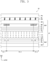
- FIG. 3 is a cross-sectional view corresponding to a line I-I' of the display device DD illustrated in FIG. 2 .
- the display device DD may comprise a liquid crystal display panel DP, a light control member LM disposed on the liquid crystal display panel DP, and a polarizing member PM.
- the liquid crystal display panel DP, the light control member LM, and the polarizing member PM may be sequentially stacked in the direction of the third directional axis DR3 that corresponds to the direction in which an image is displayed.
- the liquid crystal display panel DP may comprise a display area DA displaying an image and a non-display area NDA not displaying an image.
- the non-display area NDA may be disposed around the display area DA.
- the liquid crystal display panel DP may have a quadrilateral shape parallel to a plane defined by the first directional axis DR1 and the second directional axis DR2. However, embodiments of the present disclosure are not limited thereto. In certain embodiments, a shape of the display area DA and a shape of the non-display area NDA may be relatively and variously designed.
- the liquid crystal display panel DP may generate an image and may provide the generated image through a front surface thereof.
- the liquid crystal display panel DP may provide the generated image in the direction of the third directional axis DR3.
- the display area DA of the liquid crystal display panel DP may comprise a plurality of pixel areas PX-1, PX-2, and PX-3.
- the pixel areas PX-1, PX-2, and PX-3 may be defined by, for example, a plurality of gate lines and a plurality of data lines.
- the pixel areas PX-1, PX-2, and PX-3 may be arranged in a matrix form.
- a pixel PX (see FIG. 4A ) may be disposed in each of the pixel areas PX-1, PX-2, and PX-3.
- the pixel areas PX-1, PX-2, and PX-3 may emit or output lights of which wavelengths are different from each other.
- the liquid crystal display panel DP may comprise a blue pixel area, a green pixel area, a red pixel area, and a white pixel area.
- the pixel areas may emit or output lights of which wavelengths are different from those of the color lights described above, or neighboring pixel areas may emit or output the same wavelength of light.
- the light control member LM may be disposed on the liquid crystal display panel DP.
- the light control member LM may comprise a first optical part RD.
- the first optical part RD may have a rod shape.
- the light control member LM may be an optical layer that transmits light provided through the polarizing member PM to the liquid crystal display panel DP and transmits light outputted from the liquid crystal display panel DP to the polarizing member PM.
- the light control member LM may function as a light-scattering layer or a light-collecting layer.
- the light control member LM may collect light outputted from the liquid crystal display panel DP in the direction of the third directional axis DR3.
- the direction of the third directional axis DR3 may also be referred to as a front direction that corresponds to a direction in which an image displayed by the display device DD is outputted to the user OB.
- the polarizing member PM may be disposed on the light control member LM.
- the polarizing member PM may comprise a polarizer that linearly polarizes light provided thereto.
- the light control member LM and the polarizing member PM will be described later in more detail.
- the liquid crystal display panel DP may comprise a first substrate SUB1, a second substrate SUB2 that faces the first substrate SUB1, and a liquid crystal layer LCL disposed between the first substrate SUB1 and the second substrate SUB2.
- the first substrate SUB1 may be an upper substrate adjacent to the light control member LM
- the second substrate SUB2 may be a lower substrate.
- the first substrate SUB1 may comprise a first base substrate BS1 and a color filter layer CF that is disposed on the first base substrate BS1.
- the first substrate SUB1 may further comprise a common electrode CE that is disposed on the color filter layer CF.
- the color filter layer CF may be disposed on a bottom surface of the first base substrate BS1, and the common electrode CE may be disposed on a bottom surface of the color filter layer CF.
- the color filter layer CF may be disposed under the first base substrate BS1, and the common electrode CE may be disposed under the color filter layer CF.
- the first substrate SUB1 may further comprise a light shielding layer BM that is disposed at a boundary between the pixel areas PX-1, PX-2, and PX-3 to distinguish the pixel areas PX-1, PX-2, and PX-3 from each other.
- a light shielding layer BM that is disposed at a boundary between the pixel areas PX-1, PX-2, and PX-3 to distinguish the pixel areas PX-1, PX-2, and PX-3 from each other.
- the first substrate SUB1 may further comprise a planarization layer OC that is disposed on the color filter layer CF. Even though not shown in the drawings, the planarization layer OC may be disposed to fill an uneven portion of the color filter layer CF. The planarization layer OC may be disposed between the color filter layer CF and the common electrode CE.
- the second substrate SUB2 may face the first substrate SUB1 with the liquid crystal layer LCL interposed therebetween.
- the second substrate SUB2 may comprise a second base substrate BS2, and a reflective layer RF and a pixel electrode PE that are disposed on the second base substrate BS2.
- the first base substrate BS1 and the second base substrate BS2 may each independently be a polymer substrate, a plastic substrate, a glass substrate, or a quartz substrate.
- the first base substrate BS1 and the second base substrate BS2 may be transparent insulating substrates.
- each of the first base substrate BS1 and the second base substrate BS2 may be rigid. In other embodiments, each of the first base substrate BS1 and the second base substrate BS2 may be flexible.
- the second substrate SUB2 may further comprise an insulating layer PS that is disposed on the second base substrate BS2.
- the reflective layer RF may be disposed on the insulating layer PS and may overlap with each of the pixel areas PX-1, PX-2, and PX-3.
- the reflective layers RF may be spaced apart from each other in an area corresponding to the boundary between the pixel areas PX-1, PX-2, and PX-3.
- the pixel electrode PE may be disposed on the reflective layer RF and may overlap with each of the pixel areas PX-1, PX-2, and PX-3.
- the pixel electrode PE may cover a side surface of the reflective layer RF.
- the pixel electrodes PE may be spaced apart from each other at the boundary between the pixel areas PX-1, PX-2, and PX-3.
- the pixel electrode PE may be omitted unlike the embodiment illustrated in FIG. 3 .
- the reflective layer RF may be a reflective electrode that is used as a pixel electrode.
- a first alignment layer AL1 may be disposed on the first substrate SUB1, and a second alignment layer AL2 may be disposed on the second substrate SUB2.
- the first alignment layer AL1 may be disposed on a bottom surface of the first substrate SUB1.
- the first alignment layer AL1 may affect alignment characteristics of first liquid crystal molecules LC1 that are adjacent to the first substrate SUB1
- the second alignment layer AL2 may affect alignment characteristics of second liquid crystal molecules LC2 that are adjacent to the second substrate SUB2.
- the first alignment layer AL1 and the second alignment layer AL2 may be polyimide-based alignment layers.
- the first alignment layer AL1 and the second alignment layer AL2 may be formed of the same alignment material.
- the first alignment layer AL1 and the second alignment layer AL2 may be formed of different alignment materials from each other.
- first liquid crystal molecule does not refers to a single molecule but a portion of the liquid crystal molecules comprised in the liquid crystal layer LCL, the portion being that adjacent to the first substrate.
- second liquid crystal molecule does not refers to a single molecule but a portion of the liquid crystal molecules comprised in the liquid crystal layer LCL, the portion being that adjacent to the second substrate.
- the first liquid crystal molecule may be the same chemical compound as the second liquid crystal molecule. In other embodiments first liquid crystal molecule may be a different chemical compound from the second liquid crystal molecule.
- the first alignment layer AL1 and the second alignment layer AL2 may comprise uneven portions formed by a rubbing method.
- a rubbing direction in which the uneven portions are formed may determine alignment directions of the liquid crystal molecules that are adjacent to the first alignment layer AL1 and the second alignment layer AL2.
- the first alignment layer AL1 and the second alignment layer AL2 may determine the alignment directions of the adjacent liquid crystal molecules by a light alignment method.
- a light alignment method may be applied to adjust the alignment directions of the adjacent liquid crystal molecules.
- the same alignment method or different alignment methods may be applied to the first alignment layer AL1 and the second alignment layer AL2 to determine the alignment directions of the adjacent liquid crystal molecules.
- the rubbing method may be applied to only one of the first and second alignment layers AL1 and AL2 or may be applied to both of the first alignment layer AL1 and the second alignment layer AL2.
- the light alignment method may be applied to at least one or both of the first alignment layer AL1 and the second alignment layer AL2.
- a shape of the pixel electrode PE may be changed to determine the alignment directions of the liquid crystal molecules LC1 and LC2 of the liquid crystal layer LCL.
- the pixel electrode PE may comprise a stem portion and a branch portion, and the liquid crystal molecules LC1 and LC2 may be aligned in parallel to an extending direction of the branch portion. This will be described later in more detail.
- the first alignment layer AL1 may be disposed on the common electrode CE, and the second alignment layer AL2 may be disposed on the pixel electrode PE.
- the liquid crystal layer LCL in which the liquid crystal molecules LC1 and LC2 are arranged may be disposed between the first alignment layer AL1 and the second alignment layer AL2.
- the liquid crystal layer LCL is disposed between the first and second substrates SUB1 and SUB2 and comprises a plurality of the liquid crystal molecules LC1 and LC2.
- the liquid crystal molecules LC1 and LC2 having dielectric anisotropy may be arranged to provide the liquid crystal layer LCL.
- Commonly used liquid crystal molecules may be used in the liquid crystal layer LCL, and the liquid crystal molecules LC1 and LC2 are not limited to specific liquid crystal molecules.
- the liquid crystal molecules LC1 and LC2 may be formed of an alkenyl-based liquid crystal compound or an alkoxy-based liquid crystal compound.
- the liquid crystal display panel DP of the display device DD may be a twisted nematic (TN) mode display panel, a horizontal alignment mode display panel, a vertical alignment mode display panel, a super vertical alignment (SVA) mode display panel, a super patterned vertical alignment (S-PVA) mode display panel, an optically compensated bend (OCB) mode display panel, or an electrically controlled birefringence (ECB) mode display panel.
- TN twisted nematic
- SVA super vertical alignment
- S-PVA super patterned vertical alignment
- OCB optically compensated bend
- EBC electrically controlled birefringence
- the liquid crystal display panel DP of the display device DD may be a liquid crystal display panel that is operated by a driving method that is different from those of the above-described display panels and has a liquid crystal alignment direction that may be different from those of the above-described display panels.
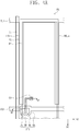
- FIG. 4A is a schematic plan view illustrating one of pixels comprised in a display device according to an embodiment of the present disclosure.
- FIG. 4B is a cross-sectional view corresponding to a line II-II' of FIG. 4A .
- FIG. 4C is a cross-sectional view corresponding to an area of FIG. 4B to illustrate a display device according to another embodiment of the present disclosure.
- One pixel is illustrated as an example in FIG. 4A , and a structure of each of other pixels may be substantially the same or similar as the structure of the pixel illustrated in FIG. 4A .
- the pixel PX connected to one of gate lines GGL and one of data lines DL is illustrated in FIG. 4A for the purpose of ease and convenience in description and illustration.
- embodiments of the present disclosure are not limited thereto.
- a plurality of pixels may be connected to one gate line and one data line, or one pixel may be connected to a plurality of gate lines and a plurality of data lines.
- the gate line GGL extends in the direction of the second directional axis DR2.
- the gate line GGL may be formed on the second base substrate BS2.
- the data line DL may extend in the direction of the first directional axis DR1 intersecting the gate line GGL.
- the pixel PX comprises a thin film transistor TFT, the pixel electrode PE connected to the thin film transistor TFT, and a storage electrode part.
- the thin film transistor TFT comprises a gate electrode GE, a gate insulating layer GI, a semiconductor pattern SM, a source electrode SE, and a drain electrode DE.
- the storage electrode part may comprise a storage line SLn extending in the direction of the second directional axis DR2 and may further comprise a first branch electrode LSLn and a second branch electrode RSLn that are branched from the storage line SLn to extend in the direction of the first directional axis DR1.
- the gate electrode GE may protrude from the gate line GGL or may be provided on a predetermined area of the gate line GGL.
- the gate electrode GE may comprise a metal.
- the gate electrode GE may be formed of at least one of nickel, chromium, molybdenum, aluminum, titanium, copper, tungsten, or any alloy thereof.
- the gate electrode GE may be formed of a single layer or multi-layer using one or more metals.
- the gate electrode GE may be formed of a triple layer comprising molybdenum, aluminum, and molybdenum that are sequentially stacked.
- the gate electrode GE may be formed of a double layer comprising titanium and copper that are sequentially stacked.
- the gate electrode GE may be a single layer formed of an alloy of titanium and copper.
- the semiconductor pattern SM is provided on the gate insulating layer GI.
- the semiconductor pattern SM is provided on the gate electrode GE with the gate insulating layer GI interposed therebetween. A portion of the semiconductor pattern SM overlaps with the gate electrode GE.
- the semiconductor pattern SM comprises an active pattern (not shown) provided on the gate insulating layer GI and an ohmic contact layer (not shown) formed on the active pattern.
- the active pattern (not shown) may be formed of an amorphous silicon thin layer, and the ohmic contact layer (not shown) may be formed of an n+ amorphous silicon thin layer.
- the ohmic contact layer (not shown) forms an ohmic contact between the active pattern and the source electrode SE and between the active pattern and the drain electrode DE.
- the source electrode SE is branched from the data line DL.
- the source electrode SE is formed on the ohmic contact layer (not shown), and a portion of the source electrode SE overlaps with the gate electrode GE.
- the data line DL may be disposed on an area of the gate insulating layer GI on which the semiconductor pattern SM is not disposed.
- the drain electrode DE is spaced apart from the source electrode SE with a portion of the semiconductor pattern SM interposed therebetween when viewed in a plan view.
- the drain electrode DE is formed on the ohmic contact layer (not shown), and a portion of the drain electrode DE overlaps with the gate electrode GE.
- the source electrode SE and the drain electrode DE may be formed of at least one of nickel, chromium, molybdenum, aluminum, titanium, copper, tungsten, or any alloy thereof.
- the source electrode SE and the drain electrode DE may be formed of a single layer or multi-layer using one or more metals.
- the source electrode SE and the drain electrode DE may be formed of a double layer comprising titanium and copper that are sequentially stacked.
- the source electrode SE and the drain electrode DE may be a single layer formed of an alloy of titanium and copper.
- a top surface of the active pattern of the semiconductor pattern SM between the source electrode SE and the drain electrode DE is exposed in the plan view, and the active pattern between the source and drain electrodes SE and DE in the plan view is defined as a channel portion in which a conductive channel is formed between the source electrode SE and the drain electrode DE when a voltage is applied to the gate electrode GE.
- the source electrode SE and the drain electrode DE overlap with portions of a remaining area of the semiconductor pattern SM except the channel portion defined between the source and drain electrodes SE and DE in the plan view.
- the pixel electrode PE is connected to the drain electrode DE with the insulating layer PS interposed therebetween.
- the pixel electrode PE partially overlaps with the storage line SLn, the first branch electrode LSLn, and the second branch electrode RSLn to form a storage capacitor.
- the insulating layer PS covers the source electrode SE, the drain electrode DE, the channel portion, and the gate insulating layer GI and has a contact hole CH exposing a portion of the drain electrode DE.
- the insulating layer PS may comprise, for example, silicon nitride or silicon oxide.
- the reflective layer RF may be disposed on the insulating layer PS.
- the reflective layer RF may be disposed between the insulating layer PS and the pixel electrode PE.
- the reflective layer RF may be formed of a metal having a high reflectance, such as aluminum, an aluminum alloy, or silver (Ag).
- the reflective layer RF overlaps with the pixel electrode PE.
- embodiments of the present disclosure are not limited thereto.
- the reflective layer RF may not be disposed in the contact hole CH.
- the pixel electrode PE is connected to the drain electrode DE through the contact hole CH that is formed in the insulating layer PS.
- the pixel electrode PE may be formed of a transparent conductive material.
- the pixel electrode PE may be formed of a transparent conductive oxide.
- the transparent conductive oxide may be indium tin oxide (ITO), indium zinc oxide (IZO), or indium tin zinc oxide (ITZO).
- FIG. 4C is a cross-sectional view illustrating a liquid crystal display panel comprised in a display device according to another embodiment.
- a liquid crystal display panel DP-1 shown the embodiment of FIG. 4C corresponds to the cross-sectional view of the liquid crystal display panel DP shown in the embodiment of FIG. 4B .
- the same descriptions as in the embodiment of FIGS. 1 to 4B will be omitted for the purpose of ease and convenience in description, and differences between the present embodiment and the embodiment of FIGS. 1 to 4B will be mainly described hereinafter.
- a color filter layer CF may be comprised in a second substrate SUB2 in the liquid crystal display panel DP-1 of the embodiment illustrated in FIG. 4C .
- the color filter layer CF may be disposed on a reflective layer RF.
- the second substrate SUB2 may comprise a second base substrate BS2, a thin film transistor TFT that is formed on the second base substrate BS2, a first insulating layer PS1, the reflective layer RF that is disposed on the first insulating layer PS1 and connected to the thin film transistor TFT through a first contact hole CH1, and the color filter layer CF and a pixel electrode PE that are formed on the reflective layer RF.
- a second insulating layer PS2 may further be disposed between the color filter layer CF and the pixel electrode PE.
- the pixel electrode PE may be electrically connected to the thin film transistor TFT through a second contact hole CH2 defined in the second insulating layer PS2.
- the pixel electrode PE may be in contact with the reflective layer RF that is exposed through the second contact hole CH2.
- a first substrate SUB1 may comprise a first base substrate BS1 and a common electrode CE.
- the liquid crystal display panel DP-1 according to the present embodiment may comprise the first base substrate BS1 and the common electrode CE that are disposed under the first base substrate BS1.
- the liquid crystal display panel DP-1 may further comprise a planarization layer OC that is disposed between the common electrode CE and the first base substrate BS1.
- the first substrate SUB1 is a color filter substrate
- the second substrate SUB2 is an array substrate. That is, the liquid crystal display panel DP of FIG. 4B is a display panel in which the color filter layer CF is formed in the upper substrate.
- the second substrate SUB2 may function as both the color filter substrate and the array substrate in the liquid crystal display panel DP-1 of the embodiment illustrated in FIG. 4C .
- the liquid crystal display panels DP and DP-1 according to the embodiments of FIGS. 4B and 4C may be reflective liquid crystal display panels comprising the reflective layer RF.
- a first alignment layer AL1 may be disposed under the first substrate SUB1, and a second alignment layer AL2 may be disposed on the second substrate SUB2.
- a liquid crystal layer LCL may be disposed between the first alignment layer AL1 and the second alignment layer AL2.
- the liquid crystal display panel comprised in the display device DD may not be limited to the embodiments illustrated in FIGS. 4B and 4C .
- reflective or transflective liquid crystal display panels having other various stack structures may be applied to the display device DD.
- a pattern shape of the reflective layer is not limited to the embodiments shown in FIGS. 4B and 4C but can be changed according to a position of a circuit layer comprising the thin film transistor, a shape of the pixel, and/or a pattern shape of the color filter layer.
- the display device according to an embodiment may further comprise a light source part, and the liquid crystal display panel of the display device may be a transflective liquid crystal display panel that displays an image using external light or light provided from the light source part of the display device.
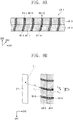
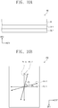
- FIG. 5A is a cross-sectional view schematically illustrating an alignment state of the first liquid crystal molecule LC1 that is adjacent to the first substrate SUB1 in the display device according to an embodiment.
- FIG. 5B is a schematic view illustrating an alignment direction of the first liquid crystal molecule LC1.
- Alignment characteristics of the first liquid crystal molecule LC1 that is adjacent to the first substrate SUB1 may be determined by the first alignment layer AL1.
- the first liquid crystal molecule LC1 may be horizontally aligned such that an alignment direction of a long axis LC-L of the first liquid crystal molecule LC1 is parallel to a flat surface (or a plane) of the first alignment layer AL1, or the first liquid crystal molecule LC1 may be vertically aligned such that the alignment direction of the long axis LC-L is perpendicular to the flat surface of the first alignment layer AL1.
- the first liquid crystal molecule LC1 that is adjacent to the first alignment layer AL1 may be disposed in parallel to the flat surface of the first alignment layer AL1 or may be disposed at a predetermined line inclination angle with respect to the flat surface of the first alignment layer AL1.
- the line inclination angle may be an angle between the long axis LC-L of the first liquid crystal molecule LC1 and one surface of the first alignment layer AL1 that is adjacent to the first liquid crystal molecule LC1.
- an angle ⁇ LC at which the first liquid crystal molecule LC1 is inclined with respect to the flat surface of the first alignment layer AL1 may correspond to the line inclination angle of the first liquid crystal molecule LC1.
- the line inclination angle ⁇ LC of the first liquid crystal molecule LC1 may be about 90 degrees.
- the line inclination angle ⁇ LC of the first liquid crystal molecule LC1 may be about 0 degree.
- the first alignment direction may represent an alignment direction of a long axis LC-L' of the first liquid crystal molecule LC1 that is projected on the first substrate SUB1.
- the first alignment direction may represent an alignment direction of the long axis LC-L' of the first liquid crystal molecule LC1 that is projected on the first alignment layer AL1.
- the alignment direction of the first liquid crystal molecule LC1 may be a direction that links from one end AA to another end BB of the first liquid crystal molecule LC1 in a direction of the long axis LC-L of the first liquid crystal molecule LC1.
- the first alignment direction of the first liquid crystal molecule LC1 in a plan view may be the alignment direction of the long axis LC-L' of the first liquid crystal molecule LC1 that is projected on the flat surface of the first alignment layer AL1.
- the first alignment direction may be a direction that links from one end AA' to another end BB' of the first liquid crystal molecule that are projected on the first alignment layer AL1.
- the long axis LC-L' of the first liquid crystal molecule LC1 that is projected on the flat surface may have an azimuth ⁇ LC .
- the azimuth ⁇ LC of the long axis LC-L' of the first liquid crystal molecule LC1 that is projected on the flat surface may represent an increasing angle with respect to a reference line RL on the flat surface in a counterclockwise direction.
- the reference line RL may be parallel to the first directional axis DR1.
- the long axis LC-L' of the first liquid crystal molecule LC1 that is projected on the flat surface may be aligned in parallel to the first directional axis DR1.
- the azimuth ⁇ LC is 90 degrees
- the long axis LC-L' of the first liquid crystal molecule LC1 that is projected on the flat surface may be aligned in parallel to the second directional axis DR2.
- the first alignment direction of the first liquid crystal molecule LC1 may be parallel to the first directional axis DR1.
- the first liquid crystal molecule LC1 that is adjacent to the first substrate may have the long axis LC-L' that is projected on the first substrate to be aligned in the first directional axis DR1.
- the first alignment direction is also referred to herein as the first direction.
- an element or component that is "parallel" to another element or component may mean that an element or component is substantially parallel to another element or component and may further mean that an optical axis or alignment direction of an element or component is substantially parallel to that of another element or component in substantially the same direction.
- the first liquid crystal molecule LC1 that is aligned by the first alignment layer AL1 is illustrated in FIGS. 5A and 5B .
- the descriptions of FIGS. 5A and 5B may also be applied to the second liquid crystal molecule LC2 adjacent to the second alignment layer AL2 (see FIG. 3 ).
- the alignment direction of the second liquid crystal molecule LC2 that is adjacent to the second alignment layer AL2 may be determined by the second alignment layer AL2.
- An alignment direction of the second liquid crystal molecule LC2 that is adjacent to the second substrate SUB2 in a plan view may represent an alignment direction of a long axis of the second liquid crystal molecule LC2 that is projected on the second substrate SUB2.
- the alignment direction of the long axis of the second liquid crystal molecule LC2 that is projected on the second substrate SUB2 is herein referred to as 'a second alignment direction.
- the second alignment direction may represent an alignment direction of a long axis of the second liquid crystal molecule LC2 that is projected on the second alignment layer AL2.
- the second alignment direction corresponding to the alignment direction of the long axis of the second liquid crystal molecule LC2 that is projected on a plane may be the same as the first alignment direction corresponding to the alignment direction of the long axis of the first liquid crystal molecule LC1 that is projected on a plane.
- the first alignment direction and the second alignment direction may be opposite to each other.
- the first alignment direction and the second alignment direction may intersect each other with a predetermined angle therebetween.
- the angle between the first alignment direction and the second alignment direction may range from 60 degrees to 90 degrees.
- An alignment direction of a liquid crystal molecule may be changed depending on physical and/or chemical properties of a surface of an alignment layer that is adjacent to the liquid crystal molecule. For example, when the surface of the alignment layer is processed by the rubbing method, the alignment direction of the liquid crystal molecule that is adjacent to the alignment layer may correspond to a rubbing direction of the alignment layer.
- FIG. 5C is a schematic view illustrating the first alignment layer AL1 and an alignment state of the first liquid crystal molecule LC1 that is aligned on the first alignment layer AL1.
- the first alignment direction of the first liquid crystal molecule LC1 may be parallel to the first rubbing direction RB.
- the first alignment direction of the first liquid crystal molecule LC1 and the first rubbing direction RB of the first alignment layer AL1 may be parallel to the first directional axis DR1.
- the first alignment direction corresponds to the alignment direction of the long axis of the first liquid crystal molecule LC1 that is projected on the first alignment layer AL1.
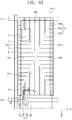
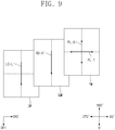
- FIG. 6A is a schematic plan view illustrating one of pixels comprised in a display device according to an embodiment of the present disclosure.
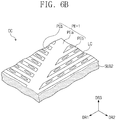
- FIG. 6B is a schematic view illustrating an alignment state of liquid crystal molecules LC in an area CC of FIG. 6A .
- FIG. 6B may illustrate an alignment state of the liquid crystal molecules LC when an electric field is applied to a pixel electrode PE-1 of a pixel PX-1.
- FIGS. 6A and 6B the same descriptions as in the embodiment of FIG. 4A will be omitted for the purpose of ease and convenience in description, and differences between the present embodiment and the embodiment of FIG. 4A will be mainly described hereinafter.
- the pixel electrode PE-1 of the pixel PX-1 of FIG. 6A may comprise a stem portion PEa and a branch portion PEb extending from the stem portion PEa.
- the pixel PX-1 illustrated in FIG. 6A may comprise a plurality of domains DM1, DM2, DM3, and DM4.
- the pixel electrode PE-1 comprises the stem portion PEa and a plurality of the branch portions PEb protruding and extending from the stem portion PEa.
- the stem portion PEa or a portion of the branch portions PEb may be connected to the drain electrode DE through the contact hole CH.
- the stem portion PEa may have various shapes.
- the stem portion PEa may have an X-shape when viewed in a plan view, as illustrated in FIG. 6A .
- the branch portions PEb do not meet each other but are spaced apart from each other.
- the branch portions PEb extend in parallel to each other in each of the domains DM1, DM2, DM3, and DM4 that are divided by the stem portion PEa.
- a spacing between the branch portions PEb that are adjacent to each other may be in the order of micrometer(s), and the spacing and pattern of the branch portions PEb may be used to align liquid crystal molecules of a liquid crystal layer LCL in a specific direction.
- the pixel PX-1 may be divided into the plurality of domains DM1, DM2, DM3, and DM4 by the stem portion PEa.
- the branch portions PEb may correspond to each of the domains DM1, DM2, DM3, and DM4, and an extending direction of the branch portions PEb in one or some of the domains DM1, DM2, DM3, and DM4 may be different from an extending direction of the branch portions PEb in another or others of the domains DM1, DM2, DM3, and DM4.
- the pixel PX-1 comprises four domains. However, embodiments of the present disclosure are not limited thereto.
- the pixel PX-1 may have various numbers of domains, for example, two, six, or eight, etc.
- a division form of the domains is not limited to the embodiment of FIG. 6A .
- the stem portion PEa may be aligned in parallel to the first directional axis DR1 or the second directional axis DR2 to separate the domains from each other.
- the liquid crystal molecule LC may represent the first liquid crystal molecule LC1 (see FIG. 3 ) or the second liquid crystal molecule LC2 (see FIG. 3 ).
- the first alignment direction of the first liquid crystal molecule LC1 may be the same as the second alignment direction of the second liquid crystal molecule LC2.
- the extending direction of the branch portions PEb may be parallel to the alignment direction of the liquid crystal molecule LC.
- the liquid crystal molecules LC may be disposed and/or aligned in parallel to the extending direction of the branch portions PEb in the display device that comprises the pixel electrode PE-1 having the branch portions PEb.
- the liquid crystal molecules LC may be aligned in parallel to the first directional axis DR1 that is parallel to the extending direction of the branch portions PEb in the first and third domains DM1 and DM3, and the liquid crystal molecules LC may be aligned in parallel to the second directional axis DR2 that is parallel to the extending direction of the branch portions PEb in the second and fourth domains DM2 and DM4.
- the first direction will be different in different areas of the liquid crystal layer LCL corresponding to different domains of the pixel PX-1.
- the extending direction of the long axis of the first optical part RD projected on the first substrate SUB1 is parallel to the first direction, in such embodiments the extending direction of the long axis of the of the first optical part RD projected on the first substrate SUB1 will also be different in different ares of the light control member corresponding to different domains of the pixel PX-1.
- the light control member LM may be disposed on the liquid crystal display panel DP in the display device DD according to an embodiment.
- the light control member LM may be disposed between the liquid crystal display panel DP and the polarizing member PM.
- the light control member LM may be an optical member that transmits light incident from the outside to the liquid crystal display panel DP and collects light that is transmitted from the liquid crystal display panel DP to the outside, in the front direction.
- the light control member LM may be an optical film that controls a traveling direction of light to transfer light that is generated in the liquid crystal display panel DP and provided as an image into a viewing range of a user.
- the light control member LM may act as the optical member that collects or concentrates light that is reflected by the reflective layer RF of the liquid crystal display panel DP and is then transmitted through the liquid crystal layer LCL in the front direction to improve the display quality of the display device DD.
- FIGS. 7A and 7B are views illustrating the light control member LM comprised in the display device according to an embodiment of the present disclosure.
- FIG. 7A is a perspective view illustrating a portion of the light control member LM according to an embodiment of the present disclosure
- FIG. 7B is a cross-sectional view illustrating the light control member LM according to an embodiment of the present disclosure.
- the light control member LM may be formed to comprise two portions having different refractive indexes from each other.
- the light control member LM may comprise a first optical part RD having a relatively high refractive index and a second optical part MT having a refractive index lower than that of the first optical part RD.
- the second optical part MT may be distinguished from the first optical part RD.
- the first optical part RD may have a rod shape
- the second optical part MT may correspond to a base part that fills a space between a plurality of the first optical parts RD.
- the first optical part RD having the rod shape may be formed of a material of which the refractive index is higher than that of the second optical part MT corresponding to the base part that arranges the first optical parts RD.
- the light control member LM may be formed of an acrylate-based material.
- the light control member LM may be formed to comprise two or more acrylate-based compounds that are different from each other.
- two kinds of acrylate-based compounds may be mixed with each other, the mixture may be phase-separated using laser light to separate the first optical part RD and the second optical part MT from each other, and then, the light control member LM may be formed by fixing the first optical part RD and the second optical part MT that are phase-separated from each other.
- the first optical part RD may be a polymer of an acrylate-based compound represented by the following chemical formula 1.
- the second optical part MT may be a polymer of an acrylate oligomer represented by the following chemical formula 2.
- 'n' may be an integer equal to or greater than 1 and equal to or less than 10.
- the compound represented by the following chemical formula 2 may be a urethane methacrylate oligomer.
- the refractive index of the first optical part RD that comprises the polymer of the acrylate-based compound represented by the chemical formula 1 may be higher than the refractive index of the second optical part MT that comprises the polymer of the acrylate-based compound represented by the chemical formula 2.
- an alignment direction RD-X of the first optical part RD may be inclined with respect to a top surface or a bottom surface of the light control member LM.
- the alignment direction of the first optical part RD may correspond to an extending direction of a long axis of the first optical part RD.
- the light control member LM may comprise the first optical part RD aligned in the direction of the first directional axis DR1 that is parallel to the first alignment direction of the first liquid crystal molecule LC1 (see FIG. 5C ) of the liquid crystal display panel.
- the light control member LM may comprise the first optical part RD and an extending direction RD-X' of a long axis of the first optical part RD may be parallel to the branch portion PEb (see FIG. 6A ) of the pixel electrode of the liquid crystal display panel.
- the light control member LM may comprise the first optical part RD an extending direction RD-X' of a long axis of the first optical part RD may be perpendicular to the branch portion PEb (see FIG. 6A ) of the pixel electrode of the liquid crystal display panel.
- an extending direction RD-X' of a long axis of the first optical part RD may be parallel to the first directional axis DR1.
- An alignment direction of the long axis of the projected first optical part RD may be defined as the extending direction RD-X' of the long axis of the first optical part RD that is projected on an imaginary plane defined by the first directional axis DR1 and the second directional axis DR2.
- the extending direction RD-X' of the long axis of the first optical part RD that is projected on an imaginary plane parallel to one surface of the first substrate SUB1 is herein referred to as 'a third alignment direction.
- the first alignment direction of the first liquid crystal molecule of the liquid crystal display panel may be parallel to the third alignment direction of the first optical part RD.
- the first alignment direction of the first liquid crystal molecule may be the same as the third alignment direction of the first optical part RD.
- an azimuth direction of the long axis of the first liquid crystal molecule LC1 that is adjacent to the first substrate SUB1 (or the upper substrate) may be parallel to an azimuth direction of the long axis of the first optical part RD that is comprised in the light control member LM.
- the azimuth direction of the long axis of the first liquid crystal molecule LC1 refers to the long axis LC-L' that is projected on a plane defined by the first directional axis DR1 and the second directional axis DR2 as shown in FIG. 5B , for example, the first alignment direction and the second alignment direction.
- the azimuth direction of the long axis of the first optical part RD refers to the projected extending direction RD-X' as shown in FIG. 7B , for example, the third alignment direction.
- the azimuth direction of the long axis of the first liquid crystal molecule LC1 that is adjacent to the first substrate SUB1 (or the upper substrate) may be substantially the same as the azimuth direction of the long axis of the first optical part RD that is comprised in the light control member LM.
- the azimuth of the long axis of the first liquid crystal molecule LC1 may be substantially equal to an azimuth of the long axis of the first optical part RD on the basis of a reference line, for example, the first directional axis DR1 or the second directional axis DR2.
- an angle between the azimuth direction of the long axis of the first liquid crystal molecule LC1 and the azimuth direction of the long axis of the first optical part RD on the basis of the reference line may be 180 degrees.
- the light control member LM may be disposed on the liquid crystal display panel and may comprise the first optical part RD having the alignment direction parallel to a first direction, and thus light can be collected or concentrated in the front direction corresponding to a display direction of an image.
- the alignment direction of the first optical part RD may correspond to the extending direction of the long axis of the first optical part RD that is projected on an imaginary plane and parallel to one surface of the first substrate of the liquid crystal display panel.
- FIG. 8A is a schematic view illustrating a light control member according to another embodiment of the present disclosure.
- FIG. 8B is a schematic view illustrating a traveling path of light when the light control member according to another embodiment is used.
- a light control member LM-1 may further comprise an auxiliary light control member LM-U.
- the auxiliary light control member LM-U may comprise an auxiliary first optical part RD-U.
- An extending direction RD-X2 of a long axis of the auxiliary first optical part RD-U may be parallel to a normal direction of a display surface of the liquid crystal display panel.
- the extending direction RD-X2 of the long axis of the auxiliary first optical part RD-U is herein referred to as 'a fourth alignment direction.
- the fourth alignment direction may be parallel to the normal direction of the display surface of the liquid crystal display panel, e.g., a normal direction of an imaginary plane that is defined by the first directional axis DR1 and the second directional axis DR2.
- the auxiliary first optical part RD-U may be aligned in a normal direction of a top surface of the light control member LM-1, and thus light provided from the liquid crystal display panel DP may pass through the light control member LM-1 to be collected or concentrated in the front direction.
- the auxiliary light control member LM-U may further comprise an auxiliary second optical part MT-U that is formed of a material having a lower refractive index than the auxiliary first optical part RD-U.
- the auxiliary second optical part MT-U may be distinguished from the auxiliary first optical part RD-U.
- the refractive index of the auxiliary first optical part RD-U may be higher than the refractive index of the auxiliary second optical part MT-U.
- the auxiliary first optical part RD-U may have a rod shape.
- the auxiliary second optical part MT-U may fill a space between a plurality of the auxiliary first optical parts RD-U.
- the light control member LM-1 illustrated in FIG. 8A may comprise a plurality of light control layers.
- the light control member LM-1 may comprise a base light control member LM-D and the auxiliary light control member LM-U that is disposed on the base light control member LM-D.
- each of the base light control member LM-D and the auxiliary light control member LM-U may function as a respective light control layer.
- the base light control member LM-D may have the same components as the light control member LM of FIGS. 7A and 7B .
- the base light control member LM-D may comprise a base first optical part RD-D and a base second optical part MT-D that are the same as the first optical part RD and the second optical part MT of FIGS. 7A and 7B , respectively.
- the base first optical part RD-D may be formed of a material having a higher refractive index than the base second optical part MT-D.
- the base first optical part RD-D may have a rod shape.
- an extending direction of a long axis of the base first optical part RD-D may correspond to the direction of the first directional axis DR1.
- the extending direction of the long axis of the base first optical part RD-D may be parallel to an alignment direction, in a plan view, of a liquid crystal molecule that is adjacent to an upper substrate of the liquid crystal display panel of the display device using the light control member LM-1.
- the alignment direction of the liquid crystal molecule in a plan view represents an alignment direction of a long axis of the liquid crystal molecule when the liquid crystal molecule is projected on the imaginary plane defined by the first directional axis DR1 and the second directional axis DR2.
- the extending direction of the long axis of the base first optical part RD-D that is projected on the imaginary plane may be the same as the alignment direction of the long axis of the liquid crystal molecule that is adjacent to the upper substrate and is projected on the same imaginary plane.
- the extending direction of the long axis of the base first optical part RD-D that is projected on the imaginary plane may be opposite to the alignment direction of the long axis of the liquid crystal molecule that is adjacent to the upper substrate and is projected on the same imaginary plane, and thus an angle therebetween maybe 180 degrees.
- incident light L in may be provided from an external light source to the liquid crystal display panel DP, and output light L R that is generated by and outputted from the liquid crystal display panel DP as an image using the incident light L in may pass through the base first optical part RD-D and the auxiliary first optical part RD-U and then may be transferred as final output light L OUT to a user.
- the base first optical part RD-D and the auxiliary first optical part RD-U are in contact or coincide with each other.
- embodiments of the present disclosure are not limited thereto.
- one surface of the base first optical part RD-D that corresponds to an exit surface of light L D passing through the base light control member LM-D may not contact or coincide with one surface of the auxiliary first optical part RD-U that corresponds to an incident surface of light Lu passing through the auxiliary light control member LM-U.
- thicknesses of the base light control member LM-D and the auxiliary light control member LM-U in the direction of the third directional axis DR3 may be equal to or different from each other.
- the base light control member LM-D and the auxiliary light control member LM-U may be formed of the same material.
- the base first optical part RD-D and the auxiliary first optical part RD-U may be formed of the same material.
- the base first optical part RD-D and the auxiliary first optical part RD-U may be formed of different materials from each other.
- FIG. 9 is a schematic view illustrating relations between optical axes in a display device according to an embodiment of the present disclosure.
- the direction of the first directional axis DR1 is 0 degree, and the angle of each of other directions is represented based on the direction of the first directional axis DR1.
- the first directional axis DR1 may be parallel to a vertical side of the liquid crystal display panel DP when the liquid crystal display panel DP is defined as a rectangular shape.
- an optical axis LC-L' illustrated in the liquid crystal display panel DP represents the first alignment direction of the first liquid crystal molecule LC1 (see FIGS. 3 and 5B ), and the first alignment direction may be parallel to the first directional axis DR1 and may have an azimuth of 0 degrees with respect to the first directional axis DR1. Unlike the embodiment of FIG. 9 , the azimuth of the first alignment direction may be 180 degrees in another embodiment.
- the optical axis RD-X' of the light control member LM represents the alignment direction of the first optical part RD (see FIGS.
- the optical axis RD-X' of the light control member LM may be parallel to the first directional axis DR1.
- the optical axis RD-X' of the light control member LM may have an azimuth of 0 degree with respect to the first directional axis DR1.
- the optical axis RD-X' of the light control member LM may be parallel to the optical axis LC-L' of the liquid crystal display panel DP.
- the azimuth of the optical axis RD-X' of the light control member LM may be substantially equal to the azimuth of the optical axis LC-L' of the liquid crystal display panel DP.
- a transmission axis PL-T and an absorption axis PL-A of the polarizing member PM are perpendicular to each other.
- the transmission axis PL-T may be parallel to the second directional axis DR2 and may be perpendicular to the optical axis RD-X' of the light control member LM and the optical axis LC-L' of the liquid crystal display panel DP.
- the transmission axis PL-T of the polarizing member PM e.g., the polarizer comprised in the polarizing member PM
- the transmission axis PL-T of the polarizer may have the azimuth of 90 degrees with respect to the first directional axis DR1.
- the optical axis RD-X' of the light control member LM and the optical axis LC-L' of the liquid crystal display panel DP may have the azimuth of 0 degree with respect to the first directional axis DR1.
- the transmission axis PL-T of the polarizer may have the azimuth of 90 degrees with respect to the first directional axis DR1
- the optical axis RD-X' of the light control member LM may have the azimuth of 0 degree with respect to the first directional axis DR1
- the optical axis LC-L' of the liquid crystal display panel DP may have the azimuth of 180 degree with respect to the first directional axis DR1.
- the transmission axis PL-T of the polarizing member PM may be parallel to a horizontal direction of the liquid crystal display panel DP when viewed in a plan view.
- the horizontal direction of the liquid crystal display panel DP may represent a horizontal direction in the display surface of the liquid crystal display panel DP, on which an image is displayed.
- the horizontal direction of the liquid crystal display panel or the horizontal direction of the display surface may correspond to a horizontal direction of the display panel in which a user views the display panel.
- the alignment direction of the liquid crystal molecule of the liquid crystal display panel DP comprising the pixel electrode PE-1 of FIG. 6A may have an azimuth of 0 degree or 90 degrees with respect to the first directional axis DR1.
- the optical axis RD-X' of the light control member LM may be parallel or perpendicular to the alignment direction of the liquid crystal molecule.
- the optical axis RD-X' of the light control member LM may have an azimuth of 0 degree with respect to the first directional axis DR1.
- the transmission axis PL-T of the polarizing member PM of the display device comprising the pixel electrode PE-1 of FIG. 6A may be parallel to the second directional axis DR2 and may be perpendicular to the optical axis RD-X' of the light control member LM.
- the transmission axis PL-T of the polarizing member PM may be parallel or perpendicular to the optical axis LC-L' of the liquid crystal display panel DP.
- the transmission axis PL-T of the polarizer may have an azimuth of 90 degrees with respect to the first directional axis DR1.
- the optical axis LC-L' of the liquid crystal display panel DP and the optical axis RD-X' of the light control member LM are parallel to each other, and thus it is possible to minimize or prevent light leakage and color deviation problems that may occur if optical axes of the liquid crystal display panel DP and the light control member LM are offset from each other.
- the transmission axis PL-T of the polarizer comprised in the polarizing member PM is perpendicular to the optical axis LC-L' of the liquid crystal display panel DP and the optical axis RD-X' of the light control member LM, and thus a contrast ratio and color reproducibility can be increased improving the display quality of the display device.
- the transmission axis PL-T of the polarizer of the polarizing member PM has the azimuth of 90 degrees in the embodiment of FIG. 9 .
- the transmission axis PL-T of the polarizer may have an azimuth of 0 degree in another embodiment.
- the transmission axis PL-T of the polarizer may be parallel to both the optical axis RD-X' of the light control member LM and the optical axis LC-L' of the liquid crystal display panel DP.
- a polarizing member used in a display device of an embodiment may comprise the polarizer and may further comprise at least one optical layer.
- FIG. 10A is a cross-sectional view illustrating a polarizing member according to an embodiment
- FIG. 10B is a schematic view illustrating relations between optical axes of a polarizer and optical layers in a polarizing member according to an embodiment.
- a polarizing member PM may comprise a polarizer PL having a transmission axis PL-T and an absorption axis PL-A that are perpendicular to each other.
- the polarizer PL may be a linear polarizer.
- the polarizer PL may be a film-type polarizer comprising an elongated polymer film.
- the polarizer PL may be a coating-type polarizer formed by a coating process.
- the polarizing member PM may further comprise a ⁇ /2 phase retardation layer OL1 and a ⁇ /4 phase (quarter-wave) retardation layer OL2.
- the a ⁇ /2 phase retardation layer OL1 may also be referred to as a half-wave retardation layer, and the a ⁇ /4 phase retardation layer OL2 may also be referred to as a quarter-wave retardation layer.
- the ⁇ /2 phase retardation layer OL1 may be disposed under the polarizer PL, and the ⁇ /4 phase retardation layer OL2 may be disposed under the ⁇ /2 phase retardation layer OL1.
- the ⁇ /2 phase retardation layer OL1 and the ⁇ /4 phase retardation layer OL2 may be optical layers that retard a phase of light provided through the polarizer PL.
- the ⁇ /2 phase retardation layer OL1 and the ⁇ /4 phase retardation layer OL2 may be provided in a film type or in a liquid crystal coating type.
- the ⁇ /2 phase retardation layer OL1 may change a polarization state of light provided through the polarizer PL.
- the ⁇ /2 phase retardation layer OL1 may change a polarization direction of linearly polarized light provided through the polarizer PL into the ⁇ /2 phase retardation layer OL1.
- the ⁇ /4 phase retardation layer OL2 may have optical anisotropy and may change a polarization state of light incident onto the ⁇ /4 phase retardation layer OL2.
- light that is transmitted through the polarizer PL and the ⁇ /2 phase retardation layer OL1 and incident onto the ⁇ /4 phase retardation layer OL2 may be changed from a linear polarization state into a circular polarization state.
- the ⁇ /4 phase retardation layer OL2 may change the circular polarization state of the light into the linear polarization state.
- the light changed into the linear polarization state through the ⁇ /4 phase retardation layer OL2 may be reflected by the liquid crystal display panel DP, for example, a reflection layer of the liquid crystal display panel DP, and pass through the ⁇ /2 phase retardation layer OL1, and thus the polarization state of the light may further be changed.
- the light may pass through the polarizer PL to be outputted to the outside of the polarizing member PM.
- the polarizing member PM may further comprise an additional optical layer.
- a protective member may further be disposed on the polarizing member PM to protect the display device.
- FIG. 10B illustrates relations between the transmission axis PL-T and the absorption axis PL-A of the polarizer PL, a first optical axis RX-1 of the ⁇ /2 phase retardation layer OL1, and a second optical axis RX-2 of the ⁇ /4 phase retardation layer OL2 of the polarizing member PM.
- the first optical axis RX-1 of the ⁇ /2 phase retardation layer OL1 and the second optical axis RX-2 of the ⁇ /4 phase retardation layer OL2 may represent a slow axis of the ⁇ /2 phase retardation layer OL1 and a slow axis of the ⁇ /4 phase retardation layer OL2, respectively.
- An angle ⁇ 1 between the transmission axis PL-T of the polarizer and the first optical axis RX-1 maybe 15° ⁇ 5°.
- An angle ⁇ 2 between the transmission axis PL-T of the polarizer and the second optical axis RX-2 may be 75° ⁇ 5°.
- An angle ⁇ 3 between the first optical axis RX-1 of the ⁇ /2 phase retardation layer and the second optical axis RX-2 of the ⁇ /4 phase retardation layer may be 60° ⁇ 5°.
- the angle ⁇ 1 between the transmission axis PL-T of the polarizer and the first optical axis RX-1 may be 15°
- the angle ⁇ 2 between the transmission axis PL-T of the polarizer and the second optical axis RX-2 may be 75°
- the angle ⁇ 3 between the first optical axis RX-1 and the second optical axis RX-2 maybe 60°.
- FIGS. 11 and 12 illustrate relations between optical axes in a display device of an embodiment when the polarizing member comprises the polarizer PL, the ⁇ /2 phase retardation layer OL1, and the ⁇ /4 phase retardation layer OL2 as shown in FIG. 10 .
- optical axes LC-L1' and LC-L2' of the liquid crystal display panel DP represent the first alignment direction of the first liquid crystal molecule and the second alignment direction of the second liquid crystal molecule, respectively.
- the first alignment direction is the alignment direction of the long axis of the first liquid crystal molecule LC1 that is projected on the first substrate SUB1
- the second alignment direction is the alignment direction of the long axis of the second liquid crystal molecule LC2 that is projected on the second substrate SUB2.
- the optical axis LC-L1' corresponding to the first alignment direction may be parallel to the first directional axis DR1 and may have an azimuth of 0 degree with respect to the first directional axis DR1.
- the first alignment direction may have an azimuth of 180 degrees.
- An angle ⁇ between the optical axis LC-L1' corresponding to the first alignment direction and the optical axis LC-L2' corresponding to the second alignment direction may range from 60 degrees to 90 degrees.
- the angle ⁇ is measured between the optical axis LC-L1' of the first alignment direction and the optical axis LC-L2' of the second alignment direction.
- the angle ⁇ represents an angle of 90 degrees or less among angles formed by two optical axes.
- the angle ⁇ between the optical axis LC-L1' corresponding to the first alignment direction and the optical axis LC-L2' corresponding to the second alignment direction may be greater than 60 degrees and less than 70 degrees.
- the optical axis RD-X' of the light control member LM may represent the alignment direction of the first optical part RD (see FIGS. 7A and 7B ) of the light control member LM, and the optical axis RD-X' representing the alignment direction of the first optical part RD (see FIGS. 7A and 7B ) may correspond to the extending direction of the long axis of the first optical part RD (see FIGS. 7A and 7B ) projected on a plane.
- the optical axis RD-X' of the light control member LM may be parallel to the first directional axis DR1.
- the optical axis RD-X' of the light control member LM may have an azimuth of 0 degree with respect to the first directional axis DR1.
- the optical axis RD-X' of the light control member LM may be parallel to the optical axis LC-L1' of the first alignment direction of the liquid crystal display panel DP.
- the azimuth of the optical axis RD-X' of the light control member LM may be substantially equal to the azimuth of the optical axis LC-L1' of the first alignment direction of the liquid crystal display panel DP.
- the transmission axis PL-T of the polarizer PL may be parallel to the second directional axis DR2 and may be perpendicular to the optical axis RD-X' of the light control member LM and the optical axis LC-L1' of the first alignment direction of the liquid crystal display panel DP.
- the transmission axis PL-T of the polarizer PL may have an azimuth of 90 degrees.
- the transmission axis PL-T of the polarizer PL may have the azimuth of 90 degrees with respect to the first directional axis DR1
- the optical axis RD-X' of the light control member LM and the optical axis LC-L1' of the first alignment direction of the liquid crystal display panel DP may have the azimuths of 0 degree with respect to the first directional axis DR1.
- the first optical axis RX-1 of the ⁇ /2 phase retardation layer OL1 forms the angle ⁇ 1 with respect to the transmission axis PL-T of the polarizer PL
- the second optical axis RX-2 of the ⁇ /4 phase retardation layer OL2 forms the angle ⁇ 2 with respect to the transmission axis PL-T of the polarizer PL.
- the angle ⁇ 1 and the angle ⁇ 2 may be 15° ⁇ 5° and 75° ⁇ 5°, respectively, as described above with reference to FIGS. 10A and 10B .
- a direction of a transmission axis of a polarizer may be different from the direction of the transmission axis PL-T of the polarizer PL shown in the embodiment of FIG. 11 .
- a transmission axis PL-T of a polarizer PL-1 may be parallel to the first directional axis DR1 and may further be parallel to the optical axis RD-X' of the light control member LM and the optical axis LC-L1' of the first alignment direction of the liquid crystal display panel DP.
- the transmission axis PL-T of the polarizer PL-1 may have an azimuth of 0 degrees.
- all of the azimuths of the transmission axis PL-T of the polarizer PL-1, the optical axis RD-X' of the light control member LM and the optical axis LC-L1' of the first alignment direction of the liquid crystal display panel DP may be 0 degree with respect to the first directional axis DR1.
- the transmission axis PL-T of the polarizer PL-1 and the optical axis RD-X' of the light control member LM may have the azimuths of 0 degree with respect to the first directional axis DR1, and the optical axis LC-L1' of the first alignment direction of the liquid crystal display panel DP may have an azimuth of 180 degrees with respect to the first directional axis DR1.
- Table 1 shows optical characteristics of the display device according to an embodiment of the present disclosure and a display device according to a comparative example.
- Table 1 shows a white reflectance WR, a black reflectance BR, a contrast ratio, CR, and color reproducibility when each of the display devices of the embodiment and the comparative example is viewed in the front direction.
- the embodiment represents a case in which the optical axis of the light control member is parallel to the first alignment direction of the liquid crystal molecule that is adjacent to the upper substrate in the liquid crystal display panel, and the transmission axis of the polarizer is perpendicular to the optical axis of the light control member.
- the embodiment of Table 1 shows optical characteristics of the display device having the relations between the optical axes illustrated in FIG. 11 .
- the comparative example represents a case in which the optical axis of the light control member is not parallel to the first alignment direction of the liquid crystal molecule that is adjacent to the upper substrate in the liquid crystal display panel.
- the optical axis of the light control member is perpendicular to the first alignment direction of the liquid crystal molecule that is adjacent to the upper substrate.
- the first alignment direction of the liquid crystal molecule is parallel to the transmission axis of the polarizer.
- the white reflectance WR and the black reflectance BR are relative reflectance values when a reflectance of light with respect to a barium sulfate (BaSO 4 ) substrate is 100%.
- BoSO 4 barium sulfate
- the contrast ratio CR and the color reproducibility of the embodiment in which the optical axis of the light control member is parallel to the direction of the optical axis of the liquid crystal molecule that is adjacent to the light control member are improved as compared with those of the comparative example in which the optical axis of the light control member is not parallel to the direction of the optical axis of the liquid crystal molecule that is adjacent to the light control member.
- the optical axis of the light control member that is projected on the plane is parallel to the alignment direction of the liquid crystal molecule that is adjacent to the light control member.
- the display device may comprise the light control member of which the optical axis on the plane is parallel to the alignment direction of the liquid crystal molecule that is adjacent to the light control member, and the polarizing member that has the transmission axis perpendicular to the optical axis of the light control member and the alignment direction of the liquid crystal molecule.
- the optical axis of the light control member that is projected on the plane is parallel to the alignment direction of the liquid crystal molecule, and thus the contrast ratio and the color reproducibility of the display device can be improved.
- the contrast ratio and the color reproducibility of the reflective liquid crystal display device can be improved by controlling or adjusting the relations between the alignment directions of the polarizing member, the light control member, and the liquid crystal molecule.
Landscapes
- Physics & Mathematics (AREA)
- Nonlinear Science (AREA)
- Chemical & Material Sciences (AREA)
- Crystallography & Structural Chemistry (AREA)
- General Physics & Mathematics (AREA)
- Optics & Photonics (AREA)
- Mathematical Physics (AREA)
- Spectroscopy & Molecular Physics (AREA)
- Geometry (AREA)
- Liquid Crystal (AREA)
- Devices For Indicating Variable Information By Combining Individual Elements (AREA)
Applications Claiming Priority (1)
| Application Number | Priority Date | Filing Date | Title |
|---|---|---|---|
| KR1020170085059A KR102416575B1 (ko) | 2017-07-04 | 2017-07-04 | 표시 장치 |
Publications (3)
| Publication Number | Publication Date |
|---|---|
| EP3425449A2 true EP3425449A2 (de) | 2019-01-09 |
| EP3425449A3 EP3425449A3 (de) | 2019-03-20 |
| EP3425449B1 EP3425449B1 (de) | 2024-04-24 |
Family
ID=62235830
Family Applications (1)
| Application Number | Title | Priority Date | Filing Date |
|---|---|---|---|
| EP18173671.1A Active EP3425449B1 (de) | 2017-07-04 | 2018-05-22 | Anzeigevorrichtung |
Country Status (4)
| Country | Link |
|---|---|
| US (1) | US10545369B2 (de) |
| EP (1) | EP3425449B1 (de) |
| KR (1) | KR102416575B1 (de) |
| CN (1) | CN109212815B (de) |
Families Citing this family (1)
| Publication number | Priority date | Publication date | Assignee | Title |
|---|---|---|---|---|
| TWI703391B (zh) * | 2019-05-10 | 2020-09-01 | 友達光電股份有限公司 | 液晶面板 |
Family Cites Families (17)
| Publication number | Priority date | Publication date | Assignee | Title |
|---|---|---|---|---|
| JPH0784252A (ja) | 1993-09-16 | 1995-03-31 | Sharp Corp | 液晶表示装置 |
| JP3538149B2 (ja) | 2001-01-30 | 2004-06-14 | Nec液晶テクノロジー株式会社 | 反射型液晶表示装置及びその製造方法 |
| GB2427033A (en) | 2005-06-07 | 2006-12-13 | Sharp Kk | A display switchable between public and private modes |
| KR100762028B1 (ko) * | 2005-10-14 | 2007-09-28 | 비오이 하이디스 테크놀로지 주식회사 | 고투과 및 광시야각을 갖는 반투과형 액정표시장치 |
| US20070252931A1 (en) * | 2006-05-01 | 2007-11-01 | Wintek Corporation | Transflective liquid crystal display device |
| US8208102B2 (en) * | 2006-07-21 | 2012-06-26 | Sharp Kabushiki Kaisha | Display device having reflective region and transmissive region |
| CN100430798C (zh) * | 2006-10-27 | 2008-11-05 | 友达光电股份有限公司 | 液晶显示器 |
| KR20080071250A (ko) * | 2007-01-30 | 2008-08-04 | 전북대학교산학협력단 | 전기 습윤 디스플레이 |
| KR101338998B1 (ko) * | 2009-12-11 | 2013-12-09 | 엘지디스플레이 주식회사 | 반사투과형 액정표시소자 |
| CN101819289A (zh) * | 2010-04-14 | 2010-09-01 | 友达光电股份有限公司 | 复合式光学膜结构 |
| JP5767195B2 (ja) * | 2012-11-05 | 2015-08-19 | 株式会社ジャパンディスプレイ | 半透過型表示装置、電子機器及び半透過型表示装置の駆動方法 |
| JP2014137467A (ja) * | 2013-01-16 | 2014-07-28 | Japan Display Inc | 表示装置 |
| WO2014148559A1 (ja) * | 2013-03-22 | 2014-09-25 | 富士フイルム株式会社 | 光学フィルム、それを用いた偏光板および液晶表示装置 |
| JP6050712B2 (ja) * | 2013-03-27 | 2016-12-21 | 株式会社ジャパンディスプレイ | 反射型液晶表示装置及び電子機器 |
| JP2015081940A (ja) * | 2013-10-21 | 2015-04-27 | 株式会社ジャパンディスプレイ | 液晶表示装置及び電子装置 |
| KR102270257B1 (ko) * | 2015-01-23 | 2021-06-28 | 삼성디스플레이 주식회사 | 표시장치 및 이를 이용한 표시장치의 구동방법 |
| KR102503756B1 (ko) * | 2015-11-04 | 2023-02-27 | 삼성디스플레이 주식회사 | 표시 장치 및 그 제조 방법 |
-
2017
- 2017-07-04 KR KR1020170085059A patent/KR102416575B1/ko active Active
-
2018
- 2018-01-24 US US15/878,556 patent/US10545369B2/en active Active
- 2018-05-22 EP EP18173671.1A patent/EP3425449B1/de active Active
- 2018-07-03 CN CN201810713875.4A patent/CN109212815B/zh active Active
Non-Patent Citations (1)
| Title |
|---|
| None |
Also Published As
| Publication number | Publication date |
|---|---|
| US10545369B2 (en) | 2020-01-28 |
| EP3425449B1 (de) | 2024-04-24 |
| KR20190004869A (ko) | 2019-01-15 |
| US20190011773A1 (en) | 2019-01-10 |
| CN109212815A (zh) | 2019-01-15 |
| EP3425449A3 (de) | 2019-03-20 |
| CN109212815B (zh) | 2023-02-03 |
| KR102416575B1 (ko) | 2022-07-11 |
Similar Documents
| Publication | Publication Date | Title |
|---|---|---|
| US8482704B2 (en) | Liquid crystal display device and manufacturing method thereof | |
| US9195109B2 (en) | In-plane switching liquid crystal display device having reflective region and transmissive region | |
| KR101299575B1 (ko) | 트랜스플렉티브 액정 디스플레이와 그 제조방법, 컴퓨터 | |
| US10788711B2 (en) | Display device comprising a liquid crystal display panel having at least two optical compensation films including a positive biaxial film and a negative biaxial film | |
| JP4193792B2 (ja) | 液晶表示パネル | |
| US8780302B2 (en) | Liquid crystal display device | |
| CN110426886B (zh) | 液晶显示面板及其驱动方法和液晶显示装置 | |
| KR20050070773A (ko) | 반사형 액정표시소자 및 반투과형 액정표시소자 | |
| EP3425449B1 (de) | Anzeigevorrichtung | |
| US9244322B2 (en) | Liquid crystal display device | |
| JP4720139B2 (ja) | 液晶表示パネル | |
| US9250486B2 (en) | Liquid crystal display device | |
| US7787083B2 (en) | Liquid crystal device and electronic apparatus | |
| JP4337854B2 (ja) | 液晶表示装置 | |
| CN100517039C (zh) | 共平面开关模式液晶显示器件及其制造方法 | |
| US8212977B2 (en) | In-plane switching mode liquid crystal display with a retardation layer formed directly on a color filter substrate in a reflection region | |
| JP2003140154A (ja) | 液晶表示装置 | |
| KR100522026B1 (ko) | 반투과 횡전계형 액정표시장치 | |
| JP5203062B2 (ja) | 液晶表示パネル | |
| JP3795178B2 (ja) | 液晶表示装置 | |
| CN101446719B (zh) | 液晶显示装置 | |
| KR101688593B1 (ko) | 횡전계 모드 반사투과형 액정표시장치 | |
| JP5177861B2 (ja) | 液晶表示装置 | |
| JP2008076503A (ja) | 液晶表示装置 |
Legal Events
| Date | Code | Title | Description |
|---|---|---|---|
| PUAI | Public reference made under article 153(3) epc to a published international application that has entered the european phase |
Free format text: ORIGINAL CODE: 0009012 |
|
| STAA | Information on the status of an ep patent application or granted ep patent |
Free format text: STATUS: THE APPLICATION HAS BEEN PUBLISHED |
|
| AK | Designated contracting states |
Kind code of ref document: A2 Designated state(s): AL AT BE BG CH CY CZ DE DK EE ES FI FR GB GR HR HU IE IS IT LI LT LU LV MC MK MT NL NO PL PT RO RS SE SI SK SM TR |
|
| AX | Request for extension of the european patent |
Extension state: BA ME |
|
| PUAL | Search report despatched |
Free format text: ORIGINAL CODE: 0009013 |
|
| AK | Designated contracting states |
Kind code of ref document: A3 Designated state(s): AL AT BE BG CH CY CZ DE DK EE ES FI FR GB GR HR HU IE IS IT LI LT LU LV MC MK MT NL NO PL PT RO RS SE SI SK SM TR |
|
| AX | Request for extension of the european patent |
Extension state: BA ME |
|
| RIC1 | Information provided on ipc code assigned before grant |
Ipc: G02F 1/139 20060101ALI20190213BHEP Ipc: G02F 1/1335 20060101AFI20190213BHEP |
|
| STAA | Information on the status of an ep patent application or granted ep patent |
Free format text: STATUS: REQUEST FOR EXAMINATION WAS MADE |
|
| 17P | Request for examination filed |
Effective date: 20190910 |
|
| RBV | Designated contracting states (corrected) |
Designated state(s): AL AT BE BG CH CY CZ DE DK EE ES FI FR GB GR HR HU IE IS IT LI LT LU LV MC MK MT NL NO PL PT RO RS SE SI SK SM TR |
|
| STAA | Information on the status of an ep patent application or granted ep patent |
Free format text: STATUS: EXAMINATION IS IN PROGRESS |
|
| 17Q | First examination report despatched |
Effective date: 20200423 |
|
| RAP1 | Party data changed (applicant data changed or rights of an application transferred) |
Owner name: TCL CHINA STAR OPTOELECTRONICS TECHNOLOGY CO., LTD. |
|
| GRAP | Despatch of communication of intention to grant a patent |
Free format text: ORIGINAL CODE: EPIDOSNIGR1 |
|
| STAA | Information on the status of an ep patent application or granted ep patent |
Free format text: STATUS: GRANT OF PATENT IS INTENDED |
|
| INTG | Intention to grant announced |
Effective date: 20231026 |
|
| GRAS | Grant fee paid |
Free format text: ORIGINAL CODE: EPIDOSNIGR3 |
|
| P01 | Opt-out of the competence of the unified patent court (upc) registered |
Effective date: 20240114 |
|
| RAP3 | Party data changed (applicant data changed or rights of an application transferred) |
Owner name: TCL CHINA STAR OPTOELECTRONICS TECHNOLOGY CO., LTD. |
|
| GRAA | (expected) grant |
Free format text: ORIGINAL CODE: 0009210 |
|
| STAA | Information on the status of an ep patent application or granted ep patent |
Free format text: STATUS: THE PATENT HAS BEEN GRANTED |
|
| AK | Designated contracting states |
Kind code of ref document: B1 Designated state(s): AL AT BE BG CH CY CZ DE DK EE ES FI FR GB GR HR HU IE IS IT LI LT LU LV MC MK MT NL NO PL PT RO RS SE SI SK SM TR |
|
| REG | Reference to a national code |
Ref country code: GB Ref legal event code: FG4D |
|
| REG | Reference to a national code |
Ref country code: CH Ref legal event code: EP |
|
| REG | Reference to a national code |
Ref country code: DE Ref legal event code: R096 Ref document number: 602018068453 Country of ref document: DE |
|
| REG | Reference to a national code |
Ref country code: IE Ref legal event code: FG4D |
|
| REG | Reference to a national code |
Ref country code: LT Ref legal event code: MG9D |
|
| REG | Reference to a national code |
Ref country code: NL Ref legal event code: MP Effective date: 20240424 |
|
| REG | Reference to a national code |
Ref country code: AT Ref legal event code: MK05 Ref document number: 1680236 Country of ref document: AT Kind code of ref document: T Effective date: 20240424 |
|
| PG25 | Lapsed in a contracting state [announced via postgrant information from national office to epo] |
Ref country code: NL Free format text: LAPSE BECAUSE OF FAILURE TO SUBMIT A TRANSLATION OF THE DESCRIPTION OR TO PAY THE FEE WITHIN THE PRESCRIBED TIME-LIMIT Effective date: 20240424 |
|
| PG25 | Lapsed in a contracting state [announced via postgrant information from national office to epo] |
Ref country code: NL Free format text: LAPSE BECAUSE OF FAILURE TO SUBMIT A TRANSLATION OF THE DESCRIPTION OR TO PAY THE FEE WITHIN THE PRESCRIBED TIME-LIMIT Effective date: 20240424 |
|
| PG25 | Lapsed in a contracting state [announced via postgrant information from national office to epo] |
Ref country code: IS Free format text: LAPSE BECAUSE OF FAILURE TO SUBMIT A TRANSLATION OF THE DESCRIPTION OR TO PAY THE FEE WITHIN THE PRESCRIBED TIME-LIMIT Effective date: 20240824 |
|
| PG25 | Lapsed in a contracting state [announced via postgrant information from national office to epo] |
Ref country code: BG Free format text: LAPSE BECAUSE OF FAILURE TO SUBMIT A TRANSLATION OF THE DESCRIPTION OR TO PAY THE FEE WITHIN THE PRESCRIBED TIME-LIMIT Effective date: 20240424 |
|
| PG25 | Lapsed in a contracting state [announced via postgrant information from national office to epo] |
Ref country code: HR Free format text: LAPSE BECAUSE OF FAILURE TO SUBMIT A TRANSLATION OF THE DESCRIPTION OR TO PAY THE FEE WITHIN THE PRESCRIBED TIME-LIMIT Effective date: 20240424 Ref country code: FI Free format text: LAPSE BECAUSE OF FAILURE TO SUBMIT A TRANSLATION OF THE DESCRIPTION OR TO PAY THE FEE WITHIN THE PRESCRIBED TIME-LIMIT Effective date: 20240424 |
|
| PG25 | Lapsed in a contracting state [announced via postgrant information from national office to epo] |
Ref country code: GR Free format text: LAPSE BECAUSE OF FAILURE TO SUBMIT A TRANSLATION OF THE DESCRIPTION OR TO PAY THE FEE WITHIN THE PRESCRIBED TIME-LIMIT Effective date: 20240725 |
|
| PG25 | Lapsed in a contracting state [announced via postgrant information from national office to epo] |
Ref country code: PT Free format text: LAPSE BECAUSE OF FAILURE TO SUBMIT A TRANSLATION OF THE DESCRIPTION OR TO PAY THE FEE WITHIN THE PRESCRIBED TIME-LIMIT Effective date: 20240826 |
|
| PG25 | Lapsed in a contracting state [announced via postgrant information from national office to epo] |
Ref country code: ES Free format text: LAPSE BECAUSE OF FAILURE TO SUBMIT A TRANSLATION OF THE DESCRIPTION OR TO PAY THE FEE WITHIN THE PRESCRIBED TIME-LIMIT Effective date: 20240424 |
|
| PG25 | Lapsed in a contracting state [announced via postgrant information from national office to epo] |
Ref country code: AT Free format text: LAPSE BECAUSE OF FAILURE TO SUBMIT A TRANSLATION OF THE DESCRIPTION OR TO PAY THE FEE WITHIN THE PRESCRIBED TIME-LIMIT Effective date: 20240424 |
|
| PG25 | Lapsed in a contracting state [announced via postgrant information from national office to epo] |
Ref country code: PL Free format text: LAPSE BECAUSE OF FAILURE TO SUBMIT A TRANSLATION OF THE DESCRIPTION OR TO PAY THE FEE WITHIN THE PRESCRIBED TIME-LIMIT Effective date: 20240424 |
|
| PG25 | Lapsed in a contracting state [announced via postgrant information from national office to epo] |
Ref country code: LV Free format text: LAPSE BECAUSE OF FAILURE TO SUBMIT A TRANSLATION OF THE DESCRIPTION OR TO PAY THE FEE WITHIN THE PRESCRIBED TIME-LIMIT Effective date: 20240424 |
|
| PG25 | Lapsed in a contracting state [announced via postgrant information from national office to epo] |
Ref country code: PT Free format text: LAPSE BECAUSE OF FAILURE TO SUBMIT A TRANSLATION OF THE DESCRIPTION OR TO PAY THE FEE WITHIN THE PRESCRIBED TIME-LIMIT Effective date: 20240826 Ref country code: PL Free format text: LAPSE BECAUSE OF FAILURE TO SUBMIT A TRANSLATION OF THE DESCRIPTION OR TO PAY THE FEE WITHIN THE PRESCRIBED TIME-LIMIT Effective date: 20240424 Ref country code: NO Free format text: LAPSE BECAUSE OF FAILURE TO SUBMIT A TRANSLATION OF THE DESCRIPTION OR TO PAY THE FEE WITHIN THE PRESCRIBED TIME-LIMIT Effective date: 20240724 Ref country code: LV Free format text: LAPSE BECAUSE OF FAILURE TO SUBMIT A TRANSLATION OF THE DESCRIPTION OR TO PAY THE FEE WITHIN THE PRESCRIBED TIME-LIMIT Effective date: 20240424 Ref country code: IS Free format text: LAPSE BECAUSE OF FAILURE TO SUBMIT A TRANSLATION OF THE DESCRIPTION OR TO PAY THE FEE WITHIN THE PRESCRIBED TIME-LIMIT Effective date: 20240824 Ref country code: HR Free format text: LAPSE BECAUSE OF FAILURE TO SUBMIT A TRANSLATION OF THE DESCRIPTION OR TO PAY THE FEE WITHIN THE PRESCRIBED TIME-LIMIT Effective date: 20240424 Ref country code: GR Free format text: LAPSE BECAUSE OF FAILURE TO SUBMIT A TRANSLATION OF THE DESCRIPTION OR TO PAY THE FEE WITHIN THE PRESCRIBED TIME-LIMIT Effective date: 20240725 Ref country code: FI Free format text: LAPSE BECAUSE OF FAILURE TO SUBMIT A TRANSLATION OF THE DESCRIPTION OR TO PAY THE FEE WITHIN THE PRESCRIBED TIME-LIMIT Effective date: 20240424 Ref country code: ES Free format text: LAPSE BECAUSE OF FAILURE TO SUBMIT A TRANSLATION OF THE DESCRIPTION OR TO PAY THE FEE WITHIN THE PRESCRIBED TIME-LIMIT Effective date: 20240424 Ref country code: BG Free format text: LAPSE BECAUSE OF FAILURE TO SUBMIT A TRANSLATION OF THE DESCRIPTION OR TO PAY THE FEE WITHIN THE PRESCRIBED TIME-LIMIT Effective date: 20240424 Ref country code: AT Free format text: LAPSE BECAUSE OF FAILURE TO SUBMIT A TRANSLATION OF THE DESCRIPTION OR TO PAY THE FEE WITHIN THE PRESCRIBED TIME-LIMIT Effective date: 20240424 Ref country code: RS Free format text: LAPSE BECAUSE OF FAILURE TO SUBMIT A TRANSLATION OF THE DESCRIPTION OR TO PAY THE FEE WITHIN THE PRESCRIBED TIME-LIMIT Effective date: 20240724 |
|
| REG | Reference to a national code |
Ref country code: CH Ref legal event code: PL |
|
| PG25 | Lapsed in a contracting state [announced via postgrant information from national office to epo] |
Ref country code: DK Free format text: LAPSE BECAUSE OF FAILURE TO SUBMIT A TRANSLATION OF THE DESCRIPTION OR TO PAY THE FEE WITHIN THE PRESCRIBED TIME-LIMIT Effective date: 20240424 |
|
| PG25 | Lapsed in a contracting state [announced via postgrant information from national office to epo] |
Ref country code: LU Free format text: LAPSE BECAUSE OF NON-PAYMENT OF DUE FEES Effective date: 20240522 |
|
| PG25 | Lapsed in a contracting state [announced via postgrant information from national office to epo] |
Ref country code: EE Free format text: LAPSE BECAUSE OF FAILURE TO SUBMIT A TRANSLATION OF THE DESCRIPTION OR TO PAY THE FEE WITHIN THE PRESCRIBED TIME-LIMIT Effective date: 20240424 |
|
| PG25 | Lapsed in a contracting state [announced via postgrant information from national office to epo] |
Ref country code: CZ Free format text: LAPSE BECAUSE OF FAILURE TO SUBMIT A TRANSLATION OF THE DESCRIPTION OR TO PAY THE FEE WITHIN THE PRESCRIBED TIME-LIMIT Effective date: 20240424 |
|
| PG25 | Lapsed in a contracting state [announced via postgrant information from national office to epo] |
Ref country code: SK Free format text: LAPSE BECAUSE OF FAILURE TO SUBMIT A TRANSLATION OF THE DESCRIPTION OR TO PAY THE FEE WITHIN THE PRESCRIBED TIME-LIMIT Effective date: 20240424 Ref country code: RO Free format text: LAPSE BECAUSE OF FAILURE TO SUBMIT A TRANSLATION OF THE DESCRIPTION OR TO PAY THE FEE WITHIN THE PRESCRIBED TIME-LIMIT Effective date: 20240424 |
|
| REG | Reference to a national code |
Ref country code: DE Ref legal event code: R097 Ref document number: 602018068453 Country of ref document: DE |
|
| PG25 | Lapsed in a contracting state [announced via postgrant information from national office to epo] |
Ref country code: SM Free format text: LAPSE BECAUSE OF FAILURE TO SUBMIT A TRANSLATION OF THE DESCRIPTION OR TO PAY THE FEE WITHIN THE PRESCRIBED TIME-LIMIT Effective date: 20240424 |
|
| PG25 | Lapsed in a contracting state [announced via postgrant information from national office to epo] |
Ref country code: SM Free format text: LAPSE BECAUSE OF FAILURE TO SUBMIT A TRANSLATION OF THE DESCRIPTION OR TO PAY THE FEE WITHIN THE PRESCRIBED TIME-LIMIT Effective date: 20240424 Ref country code: SK Free format text: LAPSE BECAUSE OF FAILURE TO SUBMIT A TRANSLATION OF THE DESCRIPTION OR TO PAY THE FEE WITHIN THE PRESCRIBED TIME-LIMIT Effective date: 20240424 Ref country code: RO Free format text: LAPSE BECAUSE OF FAILURE TO SUBMIT A TRANSLATION OF THE DESCRIPTION OR TO PAY THE FEE WITHIN THE PRESCRIBED TIME-LIMIT Effective date: 20240424 Ref country code: LU Free format text: LAPSE BECAUSE OF NON-PAYMENT OF DUE FEES Effective date: 20240522 Ref country code: EE Free format text: LAPSE BECAUSE OF FAILURE TO SUBMIT A TRANSLATION OF THE DESCRIPTION OR TO PAY THE FEE WITHIN THE PRESCRIBED TIME-LIMIT Effective date: 20240424 Ref country code: DK Free format text: LAPSE BECAUSE OF FAILURE TO SUBMIT A TRANSLATION OF THE DESCRIPTION OR TO PAY THE FEE WITHIN THE PRESCRIBED TIME-LIMIT Effective date: 20240424 Ref country code: CZ Free format text: LAPSE BECAUSE OF FAILURE TO SUBMIT A TRANSLATION OF THE DESCRIPTION OR TO PAY THE FEE WITHIN THE PRESCRIBED TIME-LIMIT Effective date: 20240424 Ref country code: CH Free format text: LAPSE BECAUSE OF NON-PAYMENT OF DUE FEES Effective date: 20240531 Ref country code: MC Free format text: LAPSE BECAUSE OF FAILURE TO SUBMIT A TRANSLATION OF THE DESCRIPTION OR TO PAY THE FEE WITHIN THE PRESCRIBED TIME-LIMIT Effective date: 20240424 |
|
| REG | Reference to a national code |
Ref country code: BE Ref legal event code: MM Effective date: 20240531 |
|
| PLBE | No opposition filed within time limit |
Free format text: ORIGINAL CODE: 0009261 |
|
| STAA | Information on the status of an ep patent application or granted ep patent |
Free format text: STATUS: NO OPPOSITION FILED WITHIN TIME LIMIT |
|
| 26N | No opposition filed |
Effective date: 20250127 |
|
| PG25 | Lapsed in a contracting state [announced via postgrant information from national office to epo] |
Ref country code: IE Free format text: LAPSE BECAUSE OF NON-PAYMENT OF DUE FEES Effective date: 20240522 |
|
| PG25 | Lapsed in a contracting state [announced via postgrant information from national office to epo] |
Ref country code: SI Free format text: LAPSE BECAUSE OF FAILURE TO SUBMIT A TRANSLATION OF THE DESCRIPTION OR TO PAY THE FEE WITHIN THE PRESCRIBED TIME-LIMIT Effective date: 20240424 Ref country code: BE Free format text: LAPSE BECAUSE OF NON-PAYMENT OF DUE FEES Effective date: 20240531 |
|
| PG25 | Lapsed in a contracting state [announced via postgrant information from national office to epo] |
Ref country code: FR Free format text: LAPSE BECAUSE OF NON-PAYMENT OF DUE FEES Effective date: 20240624 |
|
| PGFP | Annual fee paid to national office [announced via postgrant information from national office to epo] |
Ref country code: DE Payment date: 20250521 Year of fee payment: 8 |
|
| PGFP | Annual fee paid to national office [announced via postgrant information from national office to epo] |
Ref country code: GB Payment date: 20250527 Year of fee payment: 8 |
|
| PG25 | Lapsed in a contracting state [announced via postgrant information from national office to epo] |
Ref country code: CY Free format text: LAPSE BECAUSE OF FAILURE TO SUBMIT A TRANSLATION OF THE DESCRIPTION OR TO PAY THE FEE WITHIN THE PRESCRIBED TIME-LIMIT; INVALID AB INITIO Effective date: 20180522 |
|
| PG25 | Lapsed in a contracting state [announced via postgrant information from national office to epo] |
Ref country code: HU Free format text: LAPSE BECAUSE OF FAILURE TO SUBMIT A TRANSLATION OF THE DESCRIPTION OR TO PAY THE FEE WITHIN THE PRESCRIBED TIME-LIMIT; INVALID AB INITIO Effective date: 20180522 |
|
| PG25 | Lapsed in a contracting state [announced via postgrant information from national office to epo] |
Ref country code: SE Free format text: LAPSE BECAUSE OF FAILURE TO SUBMIT A TRANSLATION OF THE DESCRIPTION OR TO PAY THE FEE WITHIN THE PRESCRIBED TIME-LIMIT Effective date: 20240424 |
|
| PG25 | Lapsed in a contracting state [announced via postgrant information from national office to epo] |
Ref country code: IT Free format text: LAPSE BECAUSE OF FAILURE TO SUBMIT A TRANSLATION OF THE DESCRIPTION OR TO PAY THE FEE WITHIN THE PRESCRIBED TIME-LIMIT Effective date: 20240424 |