EP3423978B1 - Verfahren eine animation zum anzeigen wahrend dem start eines geräts - Google Patents
Verfahren eine animation zum anzeigen wahrend dem start eines geräts Download PDFInfo
- Publication number
- EP3423978B1 EP3423978B1 EP17707038.0A EP17707038A EP3423978B1 EP 3423978 B1 EP3423978 B1 EP 3423978B1 EP 17707038 A EP17707038 A EP 17707038A EP 3423978 B1 EP3423978 B1 EP 3423978B1
- Authority
- EP
- European Patent Office
- Prior art keywords
- node
- display
- access memory
- address
- random
- Prior art date
- Legal status (The legal status is an assumption and is not a legal conclusion. Google has not performed a legal analysis and makes no representation as to the accuracy of the status listed.)
- Active
Links
Images



Classifications
-
- H—ELECTRICITY
- H04—ELECTRIC COMMUNICATION TECHNIQUE
- H04N—PICTORIAL COMMUNICATION, e.g. TELEVISION
- H04N21/00—Selective content distribution, e.g. interactive television or video on demand [VOD]
- H04N21/40—Client devices specifically adapted for the reception of or interaction with content, e.g. set-top-box [STB]; Operations thereof
- H04N21/43—Processing of content or additional data, e.g. demultiplexing additional data from a digital video stream; Elementary client operations, e.g. monitoring of home network or synchronising decoder's clock; Client middleware
- H04N21/443—OS processes, e.g. booting an STB, implementing a Java virtual machine in an STB or power management in an STB
- H04N21/4432—Powering on the client, e.g. bootstrap loading using setup parameters being stored locally or received from the server
-
- G—PHYSICS
- G06—COMPUTING OR CALCULATING; COUNTING
- G06F—ELECTRIC DIGITAL DATA PROCESSING
- G06F11/00—Error detection; Error correction; Monitoring
- G06F11/30—Monitoring
- G06F11/32—Monitoring with visual or acoustical indication of the functioning of the machine
- G06F11/321—Display for diagnostics, e.g. diagnostic result display, self-test user interface
-
- G—PHYSICS
- G06—COMPUTING OR CALCULATING; COUNTING
- G06F—ELECTRIC DIGITAL DATA PROCESSING
- G06F11/00—Error detection; Error correction; Monitoring
- G06F11/30—Monitoring
- G06F11/32—Monitoring with visual or acoustical indication of the functioning of the machine
- G06F11/324—Display of status information
- G06F11/328—Computer systems status display
-
- G—PHYSICS
- G06—COMPUTING OR CALCULATING; COUNTING
- G06F—ELECTRIC DIGITAL DATA PROCESSING
- G06F9/00—Arrangements for program control, e.g. control units
- G06F9/06—Arrangements for program control, e.g. control units using stored programs, i.e. using an internal store of processing equipment to receive or retain programs
- G06F9/44—Arrangements for executing specific programs
-
- G—PHYSICS
- G06—COMPUTING OR CALCULATING; COUNTING
- G06F—ELECTRIC DIGITAL DATA PROCESSING
- G06F9/00—Arrangements for program control, e.g. control units
- G06F9/06—Arrangements for program control, e.g. control units using stored programs, i.e. using an internal store of processing equipment to receive or retain programs
- G06F9/44—Arrangements for executing specific programs
- G06F9/4401—Bootstrapping
-
- G—PHYSICS
- G06—COMPUTING OR CALCULATING; COUNTING
- G06F—ELECTRIC DIGITAL DATA PROCESSING
- G06F9/00—Arrangements for program control, e.g. control units
- G06F9/06—Arrangements for program control, e.g. control units using stored programs, i.e. using an internal store of processing equipment to receive or retain programs
- G06F9/44—Arrangements for executing specific programs
- G06F9/4401—Bootstrapping
- G06F9/4406—Loading of operating system
-
- G—PHYSICS
- G06—COMPUTING OR CALCULATING; COUNTING
- G06F—ELECTRIC DIGITAL DATA PROCESSING
- G06F9/00—Arrangements for program control, e.g. control units
- G06F9/06—Arrangements for program control, e.g. control units using stored programs, i.e. using an internal store of processing equipment to receive or retain programs
- G06F9/44—Arrangements for executing specific programs
- G06F9/445—Program loading or initiating
-
- G—PHYSICS
- G06—COMPUTING OR CALCULATING; COUNTING
- G06T—IMAGE DATA PROCESSING OR GENERATION, IN GENERAL
- G06T13/00—Animation
-
- G—PHYSICS
- G09—EDUCATION; CRYPTOGRAPHY; DISPLAY; ADVERTISING; SEALS
- G09G—ARRANGEMENTS OR CIRCUITS FOR CONTROL OF INDICATING DEVICES USING STATIC MEANS TO PRESENT VARIABLE INFORMATION
- G09G5/00—Control arrangements or circuits for visual indicators common to cathode-ray tube indicators and other visual indicators
- G09G5/36—Control arrangements or circuits for visual indicators common to cathode-ray tube indicators and other visual indicators characterised by the display of a graphic pattern, e.g. using an all-points-addressable [APA] memory
- G09G5/39—Control of the bit-mapped memory
- G09G5/393—Arrangements for updating the contents of the bit-mapped memory
-
- H—ELECTRICITY
- H04—ELECTRIC COMMUNICATION TECHNIQUE
- H04N—PICTORIAL COMMUNICATION, e.g. TELEVISION
- H04N21/00—Selective content distribution, e.g. interactive television or video on demand [VOD]
- H04N21/40—Client devices specifically adapted for the reception of or interaction with content, e.g. set-top-box [STB]; Operations thereof
- H04N21/41—Structure of client; Structure of client peripherals
- H04N21/426—Internal components of the client ; Characteristics thereof
- H04N21/42692—Internal components of the client ; Characteristics thereof for reading from or writing on a volatile storage medium, e.g. Random Access Memory [RAM]
-
- G—PHYSICS
- G06—COMPUTING OR CALCULATING; COUNTING
- G06F—ELECTRIC DIGITAL DATA PROCESSING
- G06F3/00—Input arrangements for transferring data to be processed into a form capable of being handled by the computer; Output arrangements for transferring data from processing unit to output unit, e.g. interface arrangements
- G06F3/14—Digital output to display device ; Cooperation and interconnection of the display device with other functional units
-
- G—PHYSICS
- G09—EDUCATION; CRYPTOGRAPHY; DISPLAY; ADVERTISING; SEALS
- G09G—ARRANGEMENTS OR CIRCUITS FOR CONTROL OF INDICATING DEVICES USING STATIC MEANS TO PRESENT VARIABLE INFORMATION
- G09G2330/00—Aspects of power supply; Aspects of display protection and defect management
- G09G2330/02—Details of power systems and of start or stop of display operation
- G09G2330/026—Arrangements or methods related to booting a display
-
- G—PHYSICS
- G09—EDUCATION; CRYPTOGRAPHY; DISPLAY; ADVERTISING; SEALS
- G09G—ARRANGEMENTS OR CIRCUITS FOR CONTROL OF INDICATING DEVICES USING STATIC MEANS TO PRESENT VARIABLE INFORMATION
- G09G5/00—Control arrangements or circuits for visual indicators common to cathode-ray tube indicators and other visual indicators
- G09G5/001—Arbitration of resources in a display system, e.g. control of access to frame buffer by video controller and/or main processor
-
- G—PHYSICS
- G09—EDUCATION; CRYPTOGRAPHY; DISPLAY; ADVERTISING; SEALS
- G09G—ARRANGEMENTS OR CIRCUITS FOR CONTROL OF INDICATING DEVICES USING STATIC MEANS TO PRESENT VARIABLE INFORMATION
- G09G5/00—Control arrangements or circuits for visual indicators common to cathode-ray tube indicators and other visual indicators
- G09G5/36—Control arrangements or circuits for visual indicators common to cathode-ray tube indicators and other visual indicators characterised by the display of a graphic pattern, e.g. using an all-points-addressable [APA] memory
- G09G5/39—Control of the bit-mapped memory
- G09G5/395—Arrangements specially adapted for transferring the contents of the bit-mapped memory to the screen
-
- H—ELECTRICITY
- H04—ELECTRIC COMMUNICATION TECHNIQUE
- H04L—TRANSMISSION OF DIGITAL INFORMATION, e.g. TELEGRAPHIC COMMUNICATION
- H04L49/00—Packet switching elements
- H04L49/90—Buffering arrangements
- H04L49/9015—Buffering arrangements for supporting a linked list
Definitions
- the technical field of the invention is that of electronic devices intended to be connected to a display means.
- the present invention relates to a method for displaying an animation by an electronic device for a terminal and in particular a method for displaying an animation during the start-up phase of an electronic box.
- the invention also relates to a device implementing said method.
- the startup of an electronic device is done in several steps.
- the elementary input/output system initializes the RAM.
- the elementary input/output system loads a startup program or boot program into the RAM.
- the role of this boot program is to initialize the peripherals such as a display chip and to load the operating system into RAM.
- the operating system implementing the device is not immediately operational. Consequently, during the first moments after the device is started, the operating system does not yet have access to the drivers of the display chip and therefore cannot control the display chip to provide information, for example, on the progress of the startup.
- the boot program can be programmed to statically configure the registers of the video output chip in order to display an image indicating that the device has been started.
- a display chip In order to produce an image, a display chip typically has two registers: a video output register and a display register.
- the video output register can be configured to perform progressive display or interlaced display.
- the video output register When the video output register is configured for progressive display, the display of an image is done line by line.
- the video output register is configured for interlaced display, the image is divided into a first field called an odd field comprising the odd lines of the image and a second field called an even field comprising the even lines of the image, and the display of the image is done first by displaying the odd field and then by displaying the even field.
- the display register contains a chained configuration table, otherwise called a node, this node containing in particular the memory address of the image (in the case of a progressive mode display) or of the frame to be displayed (in the case of an interlaced mode display), the choice of the display mode through the video output register conditioning the configuration of the display register.
- a node containing in particular the memory address of the image (in the case of a progressive mode display) or of the frame to be displayed (in the case of an interlaced mode display), the choice of the display mode through the video output register conditioning the configuration of the display register.
- the node contained in the display register includes the memory address of the image to be displayed, but also its own address or, in other words, the node points to itself. The display is therefore done by traversing the node continuously.
- the display register contains a first node comprising the address of the odd frame of the image to be displayed and enables the display of the odd lines of this image.
- This first node also includes the memory address of the second node.
- the second node contains the address of the even frame of the image to be displayed and enables the display of the even lines of this image.
- the second node also includes the memory address of the first node.
- the display is therefore done by traversing the first node then traversing the second node leading to the display of the odd lines then the even lines of the image to be displayed.
- the display alternates between the display of the odd lines (or odd frame) and the display of the even lines (or even frame) of the same image.
- Buffer mechanism for pel positioning of multiple video images including overlapping, on a raster-scan crt
- IBM TECHNICAL DISCLOSURE BULLETIN, INTERNATIONAL BUSINESS MACHINES CORP. (THORNWOOD) US, vol. 29, no. 11, April 1, 1987 (1987-04-01), pages 4714-4717
- the system uses five main components (Loader, VDE Buffer, Transformer, Scan Buffer, and Display) to efficiently manage the storage, transformation, and display of video defined elements (VDEs), enabling precise pixel positioning and controlled image stacking.
- the invention provides a solution to the problems mentioned above, by proposing a programming method allowing the display of an animation from the first moments of the start-up phase.
- the method also comprises a second phase of reading the n images by said display chip, said reading being done using the display register so as to display said animation.
- the n images are displayed successively, generating an animation from the first moments of the device startup.
- each node also comprises an address of at least part of an image among the n images
- the display of a succession of images giving rise to an animation is obtained.
- At least part of an image means that a node can contain the memory address of an even or odd frame of an image or the memory address of an image.
- the animation is based on static programming of the display registers and ingeniously takes advantage of the progressive or interlaced reading mode in order to display an animation. It is therefore not necessary to adapt the display chip to the method of the invention.
- the invention also provides an electronic device comprising a non-volatile memory, a random access memory and a display chip, said display chip comprising a video output register and a display register.
- the device further comprises means for implementing the method according to the invention.
- An electronic device is understood to mean any electronic device intended to be connected to a display means.
- the electronic device according to the invention may for example consist of an electronic box intended to be connected to a television such as an STB (Set Top Box).
- the display device may be incorporated into the electronic device.
- the electronic device according to the invention may consist of a smartphone.
- the term "display chip" means a chip which includes in particular one or more means of connection to a display device.
- the display chip may include an HDMI or VGA port.
- the invention also provides a computer program product comprising instructions which cause the device according to the invention to execute the steps of the display method according to the invention.
- the invention also provides a computer-readable medium, on which the computer program according to the invention is recorded.
- the display method according to one aspect of the invention may have one or more complementary characteristics among the following, considered individually or according to all technically possible combinations.
- a boot program responsible for booting an operating system is stored in the non-volatile memory, the electronic device comprising an elementary input/output system configured to load said boot program into RAM, the n images being included in said boot program such that the step of writing the n images into RAM is performed when said boot program is loaded by said elementary input/output system.
- the storage of the startup program and the images composing the animation to be displayed is carried out in a single step.
- the step of configuring the video output register and the display register is performed by the elementary input/output system.
- the display of the animation can take place as soon as the startup program is loaded.
- a boot program responsible for booting an operating system is stored in the non-volatile memory, the electronic device comprising an elementary input/output system configured to load said boot program into RAM, the n images being stored in the non-volatile memory and the step of writing the n images into RAM being done by copying the images stored in the non-volatile memory to RAM by the boot program.
- the step of configuring the video output register and the display register is performed by the startup program.
- the display of the animation can take place as soon as the startup program is loaded.
- the n images are stored in the form of compressed images.
- the memory footprint of the images thus compressed is reduced.
- the writing of the n images in the RAM is done in a dedicated area of the RAM. This prevents the memory space containing the images from being allocated to the operating system when it is loaded. The animation can therefore continue even after the operating system has loaded, which gives the operating system time to load the display chip drivers. This avoids an interruption of the animation during the startup phase.
- the configuration of the video output register during the video output register configuration step is performed such that the display is in progressive mode and that each node comprises the address of an image.
- the configuration of the video output register during the step of configuring the video output register is carried out so that the display is done in interlaced mode, the plurality of nodes comprising even nodes and odd nodes, and each odd node comprising the address of an odd frame. of an image and each even node includes the address of an even frame of an image.
- interlaced mode allows animation to be displayed in high resolution even if the bandwidth of the video connection connecting the display chip to a display medium is low.
- the invention relates to an electronic device DE comprising a non-volatile memory MN, a random access memory MV and a display chip PA, said display chip PA comprising a video output register RV and a display register RA.
- the invention also relates to a display method using a display chip intended to be implemented in such an electronic device.
- the MV RAM can consist of a dedicated memory of the PA chip or a RAM (Random Access Memory) memory intended for an operating system.
- the non-volatile memory MN can consist of a hard disk or a flash memory.
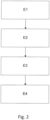
- the method according to the invention comprises a first static programming phase comprising a step E1 of configuring the RV video output register.
- This step may for example consist of configuring the RV video output register so as to obtain a progressive or interlaced display.
- the first phase of the method further comprises a step E2 of writing n images into the RAM MV, n being an integer greater than or equal to two. Since an animation consists of at least two images, it is indeed necessary in this step that the writing concerns at least two images. Thus, during this step, the images making up the animation are copied from the non-volatile memory MN to the RAM MV.
- the first phase of the method further comprises a step E3 of writing into the RAM of a plurality of nodes Ni.
- plural of nodes Ni means a chained configuration table such that each node Ni comprises the RAM address Nin of at least part of an image as well as the RAM address Nir of the following node, the last node then comprising the RAM address of the first node N1.
- the first phase of the method also comprises a step E4 of configuring the display register RA.
- This step may consist of copying into the display register RA the first node of the plurality of nodes Ni loaded into RAM.
- the method according to the invention also comprises a second phase of reading the n images by said display chip (PA), said reading being done using the display register (RA) so as to display said animation.
- the configuration of the registers is carried out statically. In other words, once configured, the registers are no longer reconfigured and the animation occurs by taking advantage of the operation of the display chip.
- the method according to the invention can be used without any particular adaptation of the display chip and allows the latter to display an animation through a static configuration of the display register and the video output register.
- the display chip PA displays the image or the image part whose address is included in a first node loaded in the display register RA. Once this image or this image part is displayed, a second node whose address in RAM MV is included in the first node is in turn loaded into the display register RA. In this way, the chip copies from the RAM into the display register successively the nodes of the plurality of nodes Ni.
- step E3 of writing the plurality of nodes Ni is a function of the display mode chosen during step E1 of configuring the video output register RV.
- the display mode is a progressive display mode.
- the writing step E3 of the plurality of nodes Ni is then performed such that each node Ni comprises the address Nin of an image as well as the address Nir of the following node, the last node comprising the address of the first node N1.
- the reading of a node Ni by the display chip PA leads to the display of an image.
- the animation will be done by the reading, by the display chip PA, of the plurality of nodes Ni. Taking the example of a refresh rate of 60 Hz, the maximum animation speed is therefore 30 cycles per second. It is however possible to envisage configuring the nodes Ni such that a plurality of nodes point to the same image in order to be able to modulate the animation speed.
- the first node N1 contains the RAM address N1n of the image I1 as well as the RAM address of the next node N2.
- Node N2 includes the RAM address of image 11 and the RAM address of the next node N3.
- the third node N3 includes the RAM address of image I2 and the RAM address of node N4.
- Node N4 includes the RAM address of image I2 and the RAM address of the first node N1, node N4 being the last node of the plurality of nodes.
- the nodes can also be configured so that the first 30 nodes contain the RAM address of a first image and the next 30 nodes contain the RAM address of a second image.
- the animation speed is only 2 images per second, in other words one animation cycle per second.
- the animation sequence can be modulated by changing the number of nodes containing the RAM address of the different images making up the animation.
- the display mode is an interlaced display mode and each image is divided into a first frame called an odd frame comprising the odd lines of the image and a second frame called an even frame comprising the even lines of the image.
- the step E3 of writing the plurality of nodes Ni is then performed such that each node Ni comprises the RAM address Nin of a frame of an image as well as the RAM address Nir of the following node, the last node comprising the RAM address Nir of the first node N1.
- nodes N1 and N3 each correspond to an odd frame Tl and nodes N2 and N4 each correspond to an even frame TP.
- the first node N1 comprises the RAM address N1n of the odd frame I1TI of a first image I1 as well as the RAM address N1r of the second node N2.
- the second node N2 comprises the RAM address of the even frame I1TP of the image I1 as well as the RAM address of node N3.
- Node N3 comprises the RAM address of the odd frame I2TI of a second image I2 as well as the RAM address of the fourth node N4.
- Node N4 comprises the RAM address of the even frame I2TP of the image I2 as well as the RAM address of the first node N1, node N4 being the last node. If we assume a 60Hz display refresh, we obtain an alternation between the two images every 1/15 of a second. In other words, the maximum animation speed is 15 cycles per second. However, we can consider configuring the Ni nodes so that a plurality of Ni nodes point to the same image in order to be able to modulate the animation speed. In other words, a first node points to the odd frame of an image and the next node points to the even frame of the same image, and this repeatedly on several consecutive pairs of nodes.
- the nodes can configure the nodes so that the first 30 nodes point to a first image (15 of the nodes pointing to the odd frame of the first image and 15 nodes pointing to the even frame of the first image) and the next 30 nodes point to a second image (15 of the nodes pointing to the odd frame of the first image and 15 nodes pointing to the even frame of the first image). So the animation speed is now only 2 frames per second. In other words, the animation speed is now only 1 cycle per second.
- step E2 of writing n images into the RAM RV can be done in two distinct ways.
- a boot program is responsible for loading an operating system into memory and the n images are stored in said boot program. The latter are therefore written in RAM MV at the same time as the boot program.
- the loading of the images in RAM MV is carried out by the elementary input/output system.
- the images being available as soon as the boot program is loaded into memory, the elementary input/output system can also be in charge of the register configuration step, which makes it possible to have a display of the animation from the first moments of booting immediately after loading the boot program, and therefore the images, in RAM MV.
- This embodiment makes it possible to load into memory all the elements necessary for the display in a single step.
- the elementary input/output system may be a BIOS (Basic Input Output System) or a security coprocessor.
- BIOS Basic Input Output System
- a safety coprocessor is a logical unit responsible for initializing the MV RAM, verifying the boot program by verifying a fingerprint of the latter, and storing the boot program in MV RAM.
- the memory size of the boot program into which the images have been incorporated may become large, which may slow down the operation of verifying the integrity of the boot program by the elementary input/output system.
- n images are stored in the non-volatile memory MN of the electronic device DE independently of the boot program and are loaded into RAM MV after the boot program has been loaded by said boot program.
- the boot program can be in charge of configuring the video output registers RV and display registers RA.
- the n images are stored as compressed images, which makes it possible to reduce the memory footprint of the images.
- a compression algorithm of the range-coding type can be considered. or LRE (for Run Length Encoding in English). More generally, any compression algorithm supported by the PA display chip can be used. It can therefore also be a proprietary compression algorithm.
- the writing of the n images in the RAM is done in a dedicated area of the RAM MV. This makes it possible to keep the images in memory once the operating system is loaded by preventing any overwriting of the images by at least part of the operating system code. Indeed, there is a delay between the moment when the operating system is loaded into memory and the moment when the operating system actually takes control of the display chip PA. Ensuring that the images remain in memory after the loading of the operating system makes it possible to guarantee that the animation will remain displayed until the effective takeover of the display chip by the operating system.
- the animation may be decomposed into a first graphics plane and a second graphics plane, the first graphics plane constituting the fixed portion of the animation and the second graphics plane constituting the changing portion of the animation, the display chip comprising means for superimposing the first graphics plane on the second graphics plane.
- the animation is only possible if the number of images is greater than three.
- the animation is broken down into two parts: a first part relating to the fixed elements of the animation which will constitute the first graphic plane, a second part relating to the mobile elements of the animation.
- the first plane will consist of the background
- the second graphic plane will consist of the flashing point.
- the display of the background i.e. the first graphic plane
- the display of the background will be done using a single node or a pair of nodes comprising the RAM address of the background image while the display of the second graphic plane will be done using a plurality of nodes Ni as explained previously.
- This is of course an example and we can envisage a second plan consisting of a more complex animation comprising a greater number of images possibly associated with a greater number of nodes.
- the step E4 of configuring the display register RA may consist of assigning a memory location of the display register RA to each graphics plane, copying into a first location of the display register RA the node (in the case of a progressive display) or the first node of the pair of nodes (in the case of an interlaced display) corresponding to the first graphics plane and copying into a second memory location of the display register RA the first node of the plurality of nodes Ni loaded into random access memory MV corresponding to the second graphics plane.
- Reading each of these memory locations is carried out in the same way as in the case of a single graphics plane described above, that is to say by displaying the image or the frame of the image whose address in random access memory MV is contained in a first node and then loading the next node whose address in random access memory MV is contained in the first node. Since reading is done simultaneously on both memory locations, two graphic planes are displayed, with the second graphic plane superimposed on the first graphic plane.
Landscapes
- Engineering & Computer Science (AREA)
- Theoretical Computer Science (AREA)
- Software Systems (AREA)
- General Physics & Mathematics (AREA)
- Physics & Mathematics (AREA)
- General Engineering & Computer Science (AREA)
- Computer Hardware Design (AREA)
- Multimedia (AREA)
- Signal Processing (AREA)
- Computer Security & Cryptography (AREA)
- Human Computer Interaction (AREA)
- Quality & Reliability (AREA)
- Computer Networks & Wireless Communication (AREA)
- Computing Systems (AREA)
- Controls And Circuits For Display Device (AREA)
- Processing Or Creating Images (AREA)
Claims (12)
- Verfahren zum Anzeigen einer Animation durch einen Anzeigechip (PA) eines elektronischen Geräts (DE), wobei das elektronische Gerät (DE) einen nichtflüchtigen Speicher (MN) und einen Arbeitsspeicher (MV) umfasst, wobei der Anzeigechip (PA) ein Videoausgaberegister (RV) und ein Anzeigeregister (RA) enthält; wobei das Verfahren beim Start des Geräts (DE) ausgeführt wird und dadurch gekennzeichnet ist, dass es eine erste Programmierungsphase umfasst, welche umfasst:- einen Schritt (E1) der Konfiguration des Videoausgaberegisters (RV), welcher derart durchgeführt wird, dass die Anzeige entweder im progressiven Modus oder im Zeilensprung-Modus erfolgt;- einen Schritt (E2) des Schreibens von n Bildern in den Arbeitsspeicher (MV), wobei n eine ganze Zahl größer oder gleich zwei ist, wobei die n Bilder, wenn sie nacheinander angezeigt werden, die anzuzeigende Animation bilden;- einen Schritt (E3) des Schreibens einer Mehrzahl von Knoten (Ni) in den Arbeitsspeicher (MV), derart dass jeder Knoten die Arbeitsspeicher-Adresse (MV-Adresse) von zumindest einem Halbbild eines Bildes aus den n Bildern sowie die Arbeitsspeicher-Adresse (MV-Adresse) des nachfolgenden Knotens umfasst, wobei der letzte Knoten die Arbeitsspeicher-Adresse (MV-Adresse) des ersten Knotens umfasst, wobei der Schritt E3 von einem im Schritt E1 ausgewählten Anzeigemodus abhängig ist;- einen Schritt (E4) der Konfiguration des Anzeigeregisters (RA), bei welchem ein Knoten aus der Mehrzahl von Knoten (Ni) in das Anzeigeregister (RA) kopiert wird;und dass es anschließend eine zweite Phase umfasst, in welcher die n Bilder von dem Anzeigechip (PA) gelesen werden, wobei die Lesephase umfasst:- einen Schritt des durch den Anzeigechip (PA) erfolgenden Anzeigens des Bildes oder Halbbilds, dessen Adresse in dem betreffenden Knoten aus der Mehrzahl von Knoten (Ni) enthalten ist, der in das Anzeigeregister (RA) geladen ist, dem sogenannten geladenen Knoten;- und sobald dieses Bild oder Halbbild angezeigt ist, einen Schritt, bei welchem der Knoten, dessen Arbeitsspeicher-Adresse ((MV-Adresse) im geladenen Knoten enthalten ist, durch den Anzeigechip (PA) in das Anzeigeregister (RA) geladen wird;wobei beide Schritte solange wiederholt werden, bis die Mehrzahl der Knoten (Ni) durchlaufen ist und die durch die aufeinanderfolgende Anzeige der n Bilder entstandene Animation angezeigt wird.
- Verfahren nach dem vorhergehenden Anspruch, dadurch gekennzeichnet, dass ein für den Start eines Betriebssystems zuständiges Startprogramm in dem nichtflüchtigen Speicher (MN) gespeichert ist, dass das elektronische Gerät (DE) ein elementares Eingabe-/Ausgabesystem enthält, das derart konfiguriert ist, dass es das Startprogramm in den Arbeitsspeicher (MV) lädt, und dass die n Bilder in dem Startprogramm enthalten sind, sodass der Schritt (E3) des Schreibens der n Bilder in den Arbeitsspeicher (MV) während des Ladens des Startprogramms durch das elementare Eingabe-/Ausgabesystem erfolgt.
- Verfahren nach Anspruch 1, dadurch gekennzeichnet, dass ein für den Start eines Betriebssystems zuständiges Startprogramm in dem nichtflüchtigen Speicher (MN) gespeichert ist, dass das elektronische Gerät (DE) ein elementares Eingabe-/Ausgabesystem enthält, das derart konfiguriert ist, dass es das Startprogramm in den Arbeitsspeicher (MV) lädt, dass die n Bilder in den nichtflüchtigen Speicher (MN) gespeichert werden, dass der Schritt (E3) des Schreibens der n Bilder in den Arbeitsspeicher dadurch erfolgt, dass die im nichtflüchtigen Speicher (MN) gespeicherten Bilder von dem betreffenden Startprogramm in den Arbeitsspeicher (MV) kopiert werden.
- Verfahren nach einem der vorhergehenden Ansprüche, dadurch gekennzeichnet, dass die n Bilder in komprimierter Form gespeichert sind.
- Verfahren nach einem der vorhergehenden Ansprüche, dadurch gekennzeichnet, dass die Termersetzung der n Bilder im Arbeitsspeicher (MV) in einem dedizierten Bereich des Arbeitsspeichers (MV) erfolgt.
- Verfahren nach einem der vorhergehenden Ansprüche, dadurch gekennzeichnet, dass das Videoausgaberegister (RV) in dem Schritt (E1) der Konfiguration des Videoausgaberegisters (RV) derart konfiguriert ist, dass die Anzeige im progressiven Modus erfolgt und dass jeder Knoten die Arbeitsspeicher-Adresse (MV-Adresse) eines Bildes umfasst.
- Verfahren nach dem vorhergehenden Anspruch, dadurch gekennzeichnet, dass die Animation in eine erste grafische Ebene und in eine zweite grafische Ebene zerlegt wird, wobei die erste grafische Ebene den festen Teil der Animation und die zweite grafische Ebene den veränderlichen Teil der Animation darstellt, wobei der Anzeigechip (PA) Mittel zum Aufeinanderlegen der ersten grafischen Ebene auf die zweite grafische Ebene enthält; und dass der Schritt (E3) des Schreibens einer Mehrzahl von Knoten (Ni) in den Arbeitsspeicher (MV) zwei Teilschritte umfasst:- einen ersten Teilschritt des Schreibens eines Knotens, der die Arbeitsspeicher-Adresse (MV-Adresse) eines in der ersten grafischen Ebene anzuzeigenden Bildes umfasst, wobei der Knoten ferner seine eigene Arbeitsspeicher-Adresse (MV-Adresse) umfasst;- einen zweiten Teilschritt des Schreibens einer Mehrzahl von Knoten (Ni), wobei jeder Knoten umfasst: die Arbeitsspeicher-Adresse (MV-Adresse) eines in der zweiten grafischen Ebene anzuzeigenden Bildes, sowie die Arbeitsspeicher-Adresse (MV-Adresse) des nachfolgenden Knotens, wobei der letzte Knoten die Arbeitsspeicher-Adresse (MV-Adresse) des ersten Knotens umfasst.
- Verfahren nach einem der Ansprüche 1 bis 5, dadurch gekennzeichnet, dass die Konfiguration des Videoausgaberegisters (RV) in dem Schritt zur Konfiguration des Videoausgaberegisters (RV) derart durchgeführt wird, dass die Anzeige im Zeilensprung-Modus erfolgt und dass die Mehrzahl von Knoten (Ni) gerade Knoten und ungerade Knoten enthält, und dass jeder ungerade Knoten die Arbeitsspeicher-Adresse (MV-Adresse) eines ungeraden Halbbilds eines Bildes umfasst, und dass jeder gerade Knoten die Arbeitsspeicher-Adresse (MV-Adresse) eines geraden Halbbilds eines Bildes umfasst.
- Verfahren nach dem vorhergehenden Anspruch, dadurch gekennzeichnet, dass die Animation in eine erste grafische Ebene und in eine zweite grafische Ebene zerlegt wird, wobei die erste grafische Ebene den festen Teil der Animation und die zweite grafische Ebene den veränderlichen Teil der Animation darstellt, wobei der Anzeigechip (PA) Mittel zum Aufeinanderlegen der ersten grafischen Ebene auf die zweite grafische Ebene enthält; und dass der Schritt (E3) des Schreibens einer Mehrzahl von Knoten (Ni) in den Arbeitsspeicher (MV) zwei Teilschritte umfasst:- einen ersten Teilschritt des Schreibens eines ersten Knotens und eines zweiten Knotens, wobei der erste Knoten die Arbeitsspeicher-Adresse (MV-Adresse) des ungeraden Halbbilds eines in der ersten grafischen Ebene anzuzeigenden Bildes sowie die Arbeitsspeicher-Adresse (MV-Adresse) des zweiten Knotens umfasst, wobei der zweite Knoten die Arbeitsspeicher-Adresse (MV-Adresse) des geraden Halbbilds des in der ersten grafischen Ebene anzuzeigenden Bildes sowie die Arbeitsspeicher-Adresse (MV-Adresse) des ersten Knotens umfasst;- einen zweiten Teilschritt des Schreibens einer Mehrzahl von Knoten (Ni), wobei jeder ungerade Knoten die Arbeitsspeicher-Adresse (MV-Adresse) des ungeraden Halbbilds eines in der zweiten grafischen Ebene anzuzeigenden Bildes umfasst, und wobei jeder gerade Knoten die Arbeitsspeicher-Adresse (MV-Adresse) des geraden Halbbilds eines in der zweiten grafischen Ebene anzuzeigenden Bildes umfasst, wobei der letzte Knoten die Arbeitsspeicher-Adresse (MV-Adresse) des ersten Knotens umfasst.
- Elektronisches Gerät (DE), das einen nichtflüchtigen Speicher (MN), einen Arbeitsspeicher (MV) und einen Anzeigechip (PA) umfasst, wobei der Anzeigechip (PA) ein Videoausgaberegister (RV) und ein Anzeigeregister (RA) enthält; wobei das Gerät dadurch gekennzeichnet ist, dass es ferner Mittel zum Ausführen des Verfahrens nach einem der Ansprüche 1 bis 9 umfasst.
- Computerprogrammprodukt, das Befehle umfasst, welche das Gerät nach Anspruch 10 dazu veranlassen, die Schritte des Verfahrens nach einem der Ansprüche 1 bis 9 auszuführen.
- Computerlesbares Speichermedium, auf welchem das Computerprogramm nach Anspruch 11 abgespeichert ist.
Applications Claiming Priority (2)
| Application Number | Priority Date | Filing Date | Title |
|---|---|---|---|
| FR1651662A FR3048293B1 (fr) | 2016-02-29 | 2016-02-29 | Procede de programmation d'une animation lors de la phase de demarrage d'un dispositif electronique et dispositif electronique associe |
| PCT/EP2017/054491 WO2017148856A1 (fr) | 2016-02-29 | 2017-02-27 | Procede de d'affichage d'une animation lors de la phase de demarrage d'un dispositif electronique et dispositif electronique associe |
Publications (2)
| Publication Number | Publication Date |
|---|---|
| EP3423978A1 EP3423978A1 (de) | 2019-01-09 |
| EP3423978B1 true EP3423978B1 (de) | 2024-12-25 |
Family
ID=56555457
Family Applications (1)
| Application Number | Title | Priority Date | Filing Date |
|---|---|---|---|
| EP17707038.0A Active EP3423978B1 (de) | 2016-02-29 | 2017-02-27 | Verfahren eine animation zum anzeigen wahrend dem start eines geräts |
Country Status (5)
| Country | Link |
|---|---|
| US (1) | US11523180B2 (de) |
| EP (1) | EP3423978B1 (de) |
| CN (1) | CN108780483B (de) |
| FR (1) | FR3048293B1 (de) |
| WO (1) | WO2017148856A1 (de) |
Families Citing this family (4)
| Publication number | Priority date | Publication date | Assignee | Title |
|---|---|---|---|---|
| WO2019112615A1 (en) * | 2017-12-08 | 2019-06-13 | Hewlett-Packard Development Company, L.P. | Private virtualized displays |
| CN109445860B (zh) * | 2018-10-17 | 2022-03-25 | 京东方科技集团股份有限公司 | 引导电子设备系统开机的方法,电子设备,可读存储介质 |
| TWI773430B (zh) * | 2021-07-09 | 2022-08-01 | 新唐科技股份有限公司 | 安全啟動系統及其方法 |
| CN121388321B (zh) * | 2025-12-23 | 2026-03-06 | 深圳市东信时代信息技术有限公司 | 基于可导出配置对象的动画编排方法、设备和存储介质 |
Family Cites Families (24)
| Publication number | Priority date | Publication date | Assignee | Title |
|---|---|---|---|---|
| US4404554A (en) * | 1980-10-06 | 1983-09-13 | Standard Microsystems Corp. | Video address generator and timer for creating a flexible CRT display |
| KR960004655B1 (ko) * | 1990-02-05 | 1996-04-11 | 가부시키가이샤 리코 | 동화 표시 장치 및 그것에 이용되는 외부 메모리 |
| US6560702B1 (en) * | 1997-12-10 | 2003-05-06 | Phoenix Technologies Ltd. | Method and apparatus for execution of an application during computer pre-boot operation |
| US6178503B1 (en) * | 1998-09-11 | 2001-01-23 | Powerquest Corporation | Managing multiple operating systems on a single computer |
| US6556193B1 (en) * | 1999-04-02 | 2003-04-29 | Teralogic, Inc. | De-interlacing video images using patch-based processing |
| US6791572B1 (en) * | 1999-06-18 | 2004-09-14 | Phoenix Technologies Ltd. | Generating media output during BIOS boot-up |
| US20020135585A1 (en) * | 2000-02-01 | 2002-09-26 | Dye Thomas A. | Video controller system with screen caching |
| US7176870B2 (en) * | 2001-12-27 | 2007-02-13 | Renesas Technology Corp. | Display drive control circuit |
| TWI286703B (en) * | 2005-07-22 | 2007-09-11 | Mitac Technology Corp | Method using foreground image data to display and background program to load and execute computer program |
| US20070110408A1 (en) * | 2005-11-14 | 2007-05-17 | Chi-Lun Chang | Device for displaying boot animation of optical disc player and method thereof |
| US8106917B2 (en) * | 2006-06-29 | 2012-01-31 | Broadcom Corporation | Method and system for mosaic mode display of video |
| CN1917571A (zh) * | 2006-09-15 | 2007-02-21 | 中辉世纪传媒发展有限公司 | 一种数字广播电视系统、机顶盒及开机画面显示方法 |
| US7987348B2 (en) * | 2007-03-30 | 2011-07-26 | Intel Corporation | Instant on video |
| US20100079472A1 (en) * | 2008-09-30 | 2010-04-01 | Sean Shang | Method and systems to display platform graphics during operating system initialization |
| JP5180874B2 (ja) * | 2009-02-27 | 2013-04-10 | 株式会社日立製作所 | バッファ管理方法、及びパケット通信装置 |
| CN101668084A (zh) * | 2009-09-18 | 2010-03-10 | 中兴通讯股份有限公司 | 一种移动终端中的个性化动画实现方法及装置 |
| CN101827199A (zh) * | 2010-04-06 | 2010-09-08 | 福建新大陆通信科技有限公司 | 通过外部存储介质实现机顶盒开机画面更换的方法 |
| US8521948B2 (en) * | 2011-01-03 | 2013-08-27 | Apple Inc. | Handling dynamic and static data for a system having non-volatile memory |
| US9883156B2 (en) * | 2011-11-30 | 2018-01-30 | Intel Corporation | Techniques to display multimedia data during operating system initialization |
| CN102768819B (zh) * | 2012-07-17 | 2014-12-10 | 中国兵器工业集团第二一四研究所苏州研发中心 | Oled实时显示驱动控制系统及其控制方法 |
| CN103581409A (zh) * | 2012-07-24 | 2014-02-12 | 上海斐讯数据通信技术有限公司 | 一种自定义开关机界面的方法和移动终端 |
| CN103150178A (zh) * | 2013-02-05 | 2013-06-12 | 联发科技(新加坡)私人有限公司 | 一种开机显示控制方法及处理器芯片 |
| US9778937B1 (en) * | 2013-10-16 | 2017-10-03 | American Megatrends, Inc. | Method and implementation for starting and stopping the playing of media content during booting process |
| US9342859B2 (en) * | 2013-10-22 | 2016-05-17 | American Megatrends, Inc. | GPU based parallel image processing at thin client |
-
2016
- 2016-02-29 FR FR1651662A patent/FR3048293B1/fr not_active Expired - Fee Related
-
2017
- 2017-02-27 CN CN201780017378.4A patent/CN108780483B/zh active Active
- 2017-02-27 US US16/080,394 patent/US11523180B2/en active Active
- 2017-02-27 WO PCT/EP2017/054491 patent/WO2017148856A1/fr not_active Ceased
- 2017-02-27 EP EP17707038.0A patent/EP3423978B1/de active Active
Also Published As
| Publication number | Publication date |
|---|---|
| CN108780483A (zh) | 2018-11-09 |
| WO2017148856A1 (fr) | 2017-09-08 |
| US11523180B2 (en) | 2022-12-06 |
| EP3423978A1 (de) | 2019-01-09 |
| US20190087200A1 (en) | 2019-03-21 |
| FR3048293A1 (fr) | 2017-09-01 |
| FR3048293B1 (fr) | 2018-07-06 |
| BR112018067555A2 (pt) | 2019-01-08 |
| CN108780483B (zh) | 2022-10-11 |
Similar Documents
| Publication | Publication Date | Title |
|---|---|---|
| FR2554256A1 (fr) | Appareil et procede de regeneration d'un tampon de trames fonctionnant a grande vitesse | |
| US8605081B2 (en) | Converting 3D data to hogel data | |
| US20100156895A1 (en) | Processing Pre-recorded Hogel Data | |
| EP3423978A1 (de) | Verfahren zur anzeige einer animation während der startphase einer elektronischen vorrichtung und entsprechende elektronische vorrichtung | |
| FR2964236A1 (fr) | Dispositif et procede de generation d'images multifenetres a priorite variable | |
| EP1432246B1 (de) | Verfahren und Gerät zur Dekodierung und zur Rückwärtsanzeige von MPEG-Bildern, Pilotvideoschaltung und ein ein solches Gerät enthaltender Dekoder | |
| EP1860571B1 (de) | DMA-Controller, einen solchen DMA-Controller umfassendes Chipsystem, Verfahren zum Datenaustausch über einen solchen DMA-Controller | |
| FR2583904A1 (fr) | Systeme d'ordinateur du type a trains multiples de donnees et instruction unique (simd), avec traitement selectif des donnees | |
| EP3686874B1 (de) | Anzeigesystem mit variabler auflösung | |
| KR101807229B1 (ko) | Tv 영상용 가속 초해상 처리 방법 및 이 방법에 따른 tv 영상용 가속 초해상 처리 장치, 제1~6 가속 초해상 처리 프로그램과 제1~2 기억 매체 | |
| CN119313797A (zh) | 全景影像的渲染方法、装置、车辆、介质及产品 | |
| CN118552394A (zh) | 图像处理方法、装置及电子设备 | |
| US12254405B2 (en) | Processing data in pixel-to-pixel neural networks | |
| EP0020980B1 (de) | Vorrichtung zur Anzeige durch Segmente | |
| FR2948473A1 (fr) | Circuit d'interface comportant une memoire de type fifo | |
| EP1752857B1 (de) | Generator von Signalen mit modifizierbarer Wellenform | |
| EP1249760A1 (de) | Multiprozessor-Datenverarbeitungsanordnung | |
| EP0680015B1 (de) | Pixelzuführgerät einer Kompressionsschaltungsoperatorsequenz sich bewegender Bilder | |
| FR2836588A1 (fr) | Procede d'affichage numerique d'image et dispositif d'affichage numerique | |
| CN114327322A (zh) | 图层显示方法及其装置 | |
| WO2016071330A1 (fr) | Procede et dispositif d'architecture configurable a gros grains pour executer en integralite un code applicatif | |
| WO2025245716A1 (en) | Oled anti-aging recording and compensation variability | |
| EP0391785B1 (de) | Gerät und Verfahren zum Schreiben in einem Silospeichergerät | |
| CN112866780B (zh) | 字幕循环显示方法及装置、视频处理设备系统和存储介质 | |
| EP0973145A1 (de) | Verfahren und Einrichtung zur Verarbeitung von digitalen Bildern resultierend aus der Einblendung von graphischen Zuzatselementen in Hauptbilder |
Legal Events
| Date | Code | Title | Description |
|---|---|---|---|
| STAA | Information on the status of an ep patent application or granted ep patent |
Free format text: STATUS: UNKNOWN |
|
| STAA | Information on the status of an ep patent application or granted ep patent |
Free format text: STATUS: THE INTERNATIONAL PUBLICATION HAS BEEN MADE |
|
| PUAI | Public reference made under article 153(3) epc to a published international application that has entered the european phase |
Free format text: ORIGINAL CODE: 0009012 |
|
| STAA | Information on the status of an ep patent application or granted ep patent |
Free format text: STATUS: REQUEST FOR EXAMINATION WAS MADE |
|
| 17P | Request for examination filed |
Effective date: 20180924 |
|
| AK | Designated contracting states |
Kind code of ref document: A1 Designated state(s): AL AT BE BG CH CY CZ DE DK EE ES FI FR GB GR HR HU IE IS IT LI LT LU LV MC MK MT NL NO PL PT RO RS SE SI SK SM TR |
|
| AX | Request for extension of the european patent |
Extension state: BA ME |
|
| DAV | Request for validation of the european patent (deleted) | ||
| DAX | Request for extension of the european patent (deleted) | ||
| STAA | Information on the status of an ep patent application or granted ep patent |
Free format text: STATUS: EXAMINATION IS IN PROGRESS |
|
| 17Q | First examination report despatched |
Effective date: 20210430 |
|
| RAP3 | Party data changed (applicant data changed or rights of an application transferred) |
Owner name: SAGEMCOM BROADBAND SAS |
|
| RIN1 | Information on inventor provided before grant (corrected) |
Inventor name: BELLANGER, JULIEN |
|
| REG | Reference to a national code |
Ref country code: DE Ref legal event code: R079 Ref document number: 602017086933 Country of ref document: DE Free format text: PREVIOUS MAIN CLASS: G06F0021510000 Ipc: H04L0049901500 |
|
| GRAP | Despatch of communication of intention to grant a patent |
Free format text: ORIGINAL CODE: EPIDOSNIGR1 |
|
| STAA | Information on the status of an ep patent application or granted ep patent |
Free format text: STATUS: GRANT OF PATENT IS INTENDED |
|
| RIC1 | Information provided on ipc code assigned before grant |
Ipc: G09G 5/393 20060101ALI20240703BHEP Ipc: G09G 5/395 20060101ALI20240703BHEP Ipc: G06F 3/14 20060101ALI20240703BHEP Ipc: G06T 13/00 20110101ALI20240703BHEP Ipc: G06F 9/445 20180101ALI20240703BHEP Ipc: G09G 5/00 20060101ALI20240703BHEP Ipc: G06F 9/44 20180101ALI20240703BHEP Ipc: H04L 49/9015 20220101AFI20240703BHEP |
|
| INTG | Intention to grant announced |
Effective date: 20240717 |
|
| GRAS | Grant fee paid |
Free format text: ORIGINAL CODE: EPIDOSNIGR3 |
|
| GRAA | (expected) grant |
Free format text: ORIGINAL CODE: 0009210 |
|
| STAA | Information on the status of an ep patent application or granted ep patent |
Free format text: STATUS: THE PATENT HAS BEEN GRANTED |
|
| AK | Designated contracting states |
Kind code of ref document: B1 Designated state(s): AL AT BE BG CH CY CZ DE DK EE ES FI FR GB GR HR HU IE IS IT LI LT LU LV MC MK MT NL NO PL PT RO RS SE SI SK SM TR |
|
| REG | Reference to a national code |
Ref country code: GB Ref legal event code: FG4D Free format text: NOT ENGLISH |
|
| REG | Reference to a national code |
Ref country code: CH Ref legal event code: EP |
|
| REG | Reference to a national code |
Ref country code: DE Ref legal event code: R096 Ref document number: 602017086933 Country of ref document: DE |
|
| REG | Reference to a national code |
Ref country code: IE Ref legal event code: FG4D Free format text: LANGUAGE OF EP DOCUMENT: FRENCH |
|
| REG | Reference to a national code |
Ref country code: LT Ref legal event code: MG9D |
|
| PG25 | Lapsed in a contracting state [announced via postgrant information from national office to epo] |
Ref country code: HR Free format text: LAPSE BECAUSE OF FAILURE TO SUBMIT A TRANSLATION OF THE DESCRIPTION OR TO PAY THE FEE WITHIN THE PRESCRIBED TIME-LIMIT Effective date: 20241225 |
|
| PGFP | Annual fee paid to national office [announced via postgrant information from national office to epo] |
Ref country code: DE Payment date: 20250122 Year of fee payment: 9 |
|
| PG25 | Lapsed in a contracting state [announced via postgrant information from national office to epo] |
Ref country code: FI Free format text: LAPSE BECAUSE OF FAILURE TO SUBMIT A TRANSLATION OF THE DESCRIPTION OR TO PAY THE FEE WITHIN THE PRESCRIBED TIME-LIMIT Effective date: 20241225 |
|
| PG25 | Lapsed in a contracting state [announced via postgrant information from national office to epo] |
Ref country code: BG Free format text: LAPSE BECAUSE OF FAILURE TO SUBMIT A TRANSLATION OF THE DESCRIPTION OR TO PAY THE FEE WITHIN THE PRESCRIBED TIME-LIMIT Effective date: 20241225 |
|
| PG25 | Lapsed in a contracting state [announced via postgrant information from national office to epo] |
Ref country code: NO Free format text: LAPSE BECAUSE OF FAILURE TO SUBMIT A TRANSLATION OF THE DESCRIPTION OR TO PAY THE FEE WITHIN THE PRESCRIBED TIME-LIMIT Effective date: 20250325 |
|
| PG25 | Lapsed in a contracting state [announced via postgrant information from national office to epo] |
Ref country code: GR Free format text: LAPSE BECAUSE OF FAILURE TO SUBMIT A TRANSLATION OF THE DESCRIPTION OR TO PAY THE FEE WITHIN THE PRESCRIBED TIME-LIMIT Effective date: 20250326 Ref country code: LV Free format text: LAPSE BECAUSE OF FAILURE TO SUBMIT A TRANSLATION OF THE DESCRIPTION OR TO PAY THE FEE WITHIN THE PRESCRIBED TIME-LIMIT Effective date: 20241225 |
|
| PGFP | Annual fee paid to national office [announced via postgrant information from national office to epo] |
Ref country code: FR Payment date: 20250121 Year of fee payment: 9 |
|
| PGFP | Annual fee paid to national office [announced via postgrant information from national office to epo] |
Ref country code: GB Payment date: 20250123 Year of fee payment: 9 |
|
| PG25 | Lapsed in a contracting state [announced via postgrant information from national office to epo] |
Ref country code: RS Free format text: LAPSE BECAUSE OF FAILURE TO SUBMIT A TRANSLATION OF THE DESCRIPTION OR TO PAY THE FEE WITHIN THE PRESCRIBED TIME-LIMIT Effective date: 20250325 |
|
| REG | Reference to a national code |
Ref country code: NL Ref legal event code: MP Effective date: 20241225 |
|
| PG25 | Lapsed in a contracting state [announced via postgrant information from national office to epo] |
Ref country code: NL Free format text: LAPSE BECAUSE OF FAILURE TO SUBMIT A TRANSLATION OF THE DESCRIPTION OR TO PAY THE FEE WITHIN THE PRESCRIBED TIME-LIMIT Effective date: 20241225 |
|
| REG | Reference to a national code |
Ref country code: AT Ref legal event code: MK05 Ref document number: 1755118 Country of ref document: AT Kind code of ref document: T Effective date: 20241225 |
|
| PG25 | Lapsed in a contracting state [announced via postgrant information from national office to epo] |
Ref country code: SM Free format text: LAPSE BECAUSE OF FAILURE TO SUBMIT A TRANSLATION OF THE DESCRIPTION OR TO PAY THE FEE WITHIN THE PRESCRIBED TIME-LIMIT Effective date: 20241225 |
|
| PG25 | Lapsed in a contracting state [announced via postgrant information from national office to epo] |
Ref country code: PL Free format text: LAPSE BECAUSE OF FAILURE TO SUBMIT A TRANSLATION OF THE DESCRIPTION OR TO PAY THE FEE WITHIN THE PRESCRIBED TIME-LIMIT Effective date: 20241225 |
|
| PG25 | Lapsed in a contracting state [announced via postgrant information from national office to epo] |
Ref country code: ES Free format text: LAPSE BECAUSE OF FAILURE TO SUBMIT A TRANSLATION OF THE DESCRIPTION OR TO PAY THE FEE WITHIN THE PRESCRIBED TIME-LIMIT Effective date: 20241225 |
|
| PG25 | Lapsed in a contracting state [announced via postgrant information from national office to epo] |
Ref country code: IS Free format text: LAPSE BECAUSE OF FAILURE TO SUBMIT A TRANSLATION OF THE DESCRIPTION OR TO PAY THE FEE WITHIN THE PRESCRIBED TIME-LIMIT Effective date: 20250425 |
|
| PG25 | Lapsed in a contracting state [announced via postgrant information from national office to epo] |
Ref country code: PT Free format text: LAPSE BECAUSE OF FAILURE TO SUBMIT A TRANSLATION OF THE DESCRIPTION OR TO PAY THE FEE WITHIN THE PRESCRIBED TIME-LIMIT Effective date: 20250428 |
|
| PG25 | Lapsed in a contracting state [announced via postgrant information from national office to epo] |
Ref country code: EE Free format text: LAPSE BECAUSE OF FAILURE TO SUBMIT A TRANSLATION OF THE DESCRIPTION OR TO PAY THE FEE WITHIN THE PRESCRIBED TIME-LIMIT Effective date: 20241225 |
|
| PG25 | Lapsed in a contracting state [announced via postgrant information from national office to epo] |
Ref country code: AT Free format text: LAPSE BECAUSE OF FAILURE TO SUBMIT A TRANSLATION OF THE DESCRIPTION OR TO PAY THE FEE WITHIN THE PRESCRIBED TIME-LIMIT Effective date: 20241225 Ref country code: RO Free format text: LAPSE BECAUSE OF FAILURE TO SUBMIT A TRANSLATION OF THE DESCRIPTION OR TO PAY THE FEE WITHIN THE PRESCRIBED TIME-LIMIT Effective date: 20241225 |
|
| PG25 | Lapsed in a contracting state [announced via postgrant information from national office to epo] |
Ref country code: SK Free format text: LAPSE BECAUSE OF FAILURE TO SUBMIT A TRANSLATION OF THE DESCRIPTION OR TO PAY THE FEE WITHIN THE PRESCRIBED TIME-LIMIT Effective date: 20241225 |
|
| PG25 | Lapsed in a contracting state [announced via postgrant information from national office to epo] |
Ref country code: CZ Free format text: LAPSE BECAUSE OF FAILURE TO SUBMIT A TRANSLATION OF THE DESCRIPTION OR TO PAY THE FEE WITHIN THE PRESCRIBED TIME-LIMIT Effective date: 20241225 |
|
| PG25 | Lapsed in a contracting state [announced via postgrant information from national office to epo] |
Ref country code: IT Free format text: LAPSE BECAUSE OF FAILURE TO SUBMIT A TRANSLATION OF THE DESCRIPTION OR TO PAY THE FEE WITHIN THE PRESCRIBED TIME-LIMIT Effective date: 20241225 |
|
| PG25 | Lapsed in a contracting state [announced via postgrant information from national office to epo] |
Ref country code: SE Free format text: LAPSE BECAUSE OF FAILURE TO SUBMIT A TRANSLATION OF THE DESCRIPTION OR TO PAY THE FEE WITHIN THE PRESCRIBED TIME-LIMIT Effective date: 20241225 |
|
| PG25 | Lapsed in a contracting state [announced via postgrant information from national office to epo] |
Ref country code: MC Free format text: LAPSE BECAUSE OF FAILURE TO SUBMIT A TRANSLATION OF THE DESCRIPTION OR TO PAY THE FEE WITHIN THE PRESCRIBED TIME-LIMIT Effective date: 20241225 |
|
| REG | Reference to a national code |
Ref country code: DE Ref legal event code: R097 Ref document number: 602017086933 Country of ref document: DE |
|
| REG | Reference to a national code |
Ref country code: CH Ref legal event code: PL |
|
| PG25 | Lapsed in a contracting state [announced via postgrant information from national office to epo] |
Ref country code: DK Free format text: LAPSE BECAUSE OF FAILURE TO SUBMIT A TRANSLATION OF THE DESCRIPTION OR TO PAY THE FEE WITHIN THE PRESCRIBED TIME-LIMIT Effective date: 20241225 |
|
| PG25 | Lapsed in a contracting state [announced via postgrant information from national office to epo] |
Ref country code: LU Free format text: LAPSE BECAUSE OF NON-PAYMENT OF DUE FEES Effective date: 20250227 |
|
| PG25 | Lapsed in a contracting state [announced via postgrant information from national office to epo] |
Ref country code: CH Free format text: LAPSE BECAUSE OF NON-PAYMENT OF DUE FEES Effective date: 20250228 |
|
| PLBE | No opposition filed within time limit |
Free format text: ORIGINAL CODE: 0009261 |
|
| STAA | Information on the status of an ep patent application or granted ep patent |
Free format text: STATUS: NO OPPOSITION FILED WITHIN TIME LIMIT |
|
| 26N | No opposition filed |
Effective date: 20250926 |
|
| REG | Reference to a national code |
Ref country code: BE Ref legal event code: MM Effective date: 20250228 |
|
| PG25 | Lapsed in a contracting state [announced via postgrant information from national office to epo] |
Ref country code: BE Free format text: LAPSE BECAUSE OF NON-PAYMENT OF DUE FEES Effective date: 20250228 |
|
| PG25 | Lapsed in a contracting state [announced via postgrant information from national office to epo] |
Ref country code: IE Free format text: LAPSE BECAUSE OF NON-PAYMENT OF DUE FEES Effective date: 20250227 |