EP3422335A1 - Electroluminescence display and method for driving the same - Google Patents
Electroluminescence display and method for driving the same Download PDFInfo
- Publication number
- EP3422335A1 EP3422335A1 EP18176258.4A EP18176258A EP3422335A1 EP 3422335 A1 EP3422335 A1 EP 3422335A1 EP 18176258 A EP18176258 A EP 18176258A EP 3422335 A1 EP3422335 A1 EP 3422335A1
- Authority
- EP
- European Patent Office
- Prior art keywords
- thin film
- film transistor
- gate
- voltage
- driving thin
- Prior art date
- Legal status (The legal status is an assumption and is not a legal conclusion. Google has not performed a legal analysis and makes no representation as to the accuracy of the status listed.)
- Ceased
Links
Images



Classifications
-
- G—PHYSICS
- G09—EDUCATION; CRYPTOGRAPHY; DISPLAY; ADVERTISING; SEALS
- G09G—ARRANGEMENTS OR CIRCUITS FOR CONTROL OF INDICATING DEVICES USING STATIC MEANS TO PRESENT VARIABLE INFORMATION
- G09G3/00—Control arrangements or circuits, of interest only in connection with visual indicators other than cathode-ray tubes
- G09G3/20—Control arrangements or circuits, of interest only in connection with visual indicators other than cathode-ray tubes for presentation of an assembly of a number of characters, e.g. a page, by composing the assembly by combination of individual elements arranged in a matrix no fixed position being assigned to or needed to be assigned to the individual characters or partial characters
- G09G3/22—Control arrangements or circuits, of interest only in connection with visual indicators other than cathode-ray tubes for presentation of an assembly of a number of characters, e.g. a page, by composing the assembly by combination of individual elements arranged in a matrix no fixed position being assigned to or needed to be assigned to the individual characters or partial characters using controlled light sources
- G09G3/30—Control arrangements or circuits, of interest only in connection with visual indicators other than cathode-ray tubes for presentation of an assembly of a number of characters, e.g. a page, by composing the assembly by combination of individual elements arranged in a matrix no fixed position being assigned to or needed to be assigned to the individual characters or partial characters using controlled light sources using electroluminescent panels
- G09G3/32—Control arrangements or circuits, of interest only in connection with visual indicators other than cathode-ray tubes for presentation of an assembly of a number of characters, e.g. a page, by composing the assembly by combination of individual elements arranged in a matrix no fixed position being assigned to or needed to be assigned to the individual characters or partial characters using controlled light sources using electroluminescent panels semiconductive, e.g. using light-emitting diodes [LED]
- G09G3/3208—Control arrangements or circuits, of interest only in connection with visual indicators other than cathode-ray tubes for presentation of an assembly of a number of characters, e.g. a page, by composing the assembly by combination of individual elements arranged in a matrix no fixed position being assigned to or needed to be assigned to the individual characters or partial characters using controlled light sources using electroluminescent panels semiconductive, e.g. using light-emitting diodes [LED] organic, e.g. using organic light-emitting diodes [OLED]
- G09G3/3225—Control arrangements or circuits, of interest only in connection with visual indicators other than cathode-ray tubes for presentation of an assembly of a number of characters, e.g. a page, by composing the assembly by combination of individual elements arranged in a matrix no fixed position being assigned to or needed to be assigned to the individual characters or partial characters using controlled light sources using electroluminescent panels semiconductive, e.g. using light-emitting diodes [LED] organic, e.g. using organic light-emitting diodes [OLED] using an active matrix
- G09G3/3233—Control arrangements or circuits, of interest only in connection with visual indicators other than cathode-ray tubes for presentation of an assembly of a number of characters, e.g. a page, by composing the assembly by combination of individual elements arranged in a matrix no fixed position being assigned to or needed to be assigned to the individual characters or partial characters using controlled light sources using electroluminescent panels semiconductive, e.g. using light-emitting diodes [LED] organic, e.g. using organic light-emitting diodes [OLED] using an active matrix with pixel circuitry controlling the current through the light-emitting element
-
- H—ELECTRICITY
- H10—SEMICONDUCTOR DEVICES; ELECTRIC SOLID-STATE DEVICES NOT OTHERWISE PROVIDED FOR
- H10K—ORGANIC ELECTRIC SOLID-STATE DEVICES
- H10K59/00—Integrated devices, or assemblies of multiple devices, comprising at least one organic light-emitting element covered by group H10K50/00
- H10K59/10—OLED displays
- H10K59/12—Active-matrix OLED [AMOLED] displays
- H10K59/131—Interconnections, e.g. wiring lines or terminals
-
- G—PHYSICS
- G09—EDUCATION; CRYPTOGRAPHY; DISPLAY; ADVERTISING; SEALS
- G09G—ARRANGEMENTS OR CIRCUITS FOR CONTROL OF INDICATING DEVICES USING STATIC MEANS TO PRESENT VARIABLE INFORMATION
- G09G3/00—Control arrangements or circuits, of interest only in connection with visual indicators other than cathode-ray tubes
- G09G3/20—Control arrangements or circuits, of interest only in connection with visual indicators other than cathode-ray tubes for presentation of an assembly of a number of characters, e.g. a page, by composing the assembly by combination of individual elements arranged in a matrix no fixed position being assigned to or needed to be assigned to the individual characters or partial characters
- G09G3/22—Control arrangements or circuits, of interest only in connection with visual indicators other than cathode-ray tubes for presentation of an assembly of a number of characters, e.g. a page, by composing the assembly by combination of individual elements arranged in a matrix no fixed position being assigned to or needed to be assigned to the individual characters or partial characters using controlled light sources
- G09G3/30—Control arrangements or circuits, of interest only in connection with visual indicators other than cathode-ray tubes for presentation of an assembly of a number of characters, e.g. a page, by composing the assembly by combination of individual elements arranged in a matrix no fixed position being assigned to or needed to be assigned to the individual characters or partial characters using controlled light sources using electroluminescent panels
- G09G3/32—Control arrangements or circuits, of interest only in connection with visual indicators other than cathode-ray tubes for presentation of an assembly of a number of characters, e.g. a page, by composing the assembly by combination of individual elements arranged in a matrix no fixed position being assigned to or needed to be assigned to the individual characters or partial characters using controlled light sources using electroluminescent panels semiconductive, e.g. using light-emitting diodes [LED]
- G09G3/3208—Control arrangements or circuits, of interest only in connection with visual indicators other than cathode-ray tubes for presentation of an assembly of a number of characters, e.g. a page, by composing the assembly by combination of individual elements arranged in a matrix no fixed position being assigned to or needed to be assigned to the individual characters or partial characters using controlled light sources using electroluminescent panels semiconductive, e.g. using light-emitting diodes [LED] organic, e.g. using organic light-emitting diodes [OLED]
- G09G3/3225—Control arrangements or circuits, of interest only in connection with visual indicators other than cathode-ray tubes for presentation of an assembly of a number of characters, e.g. a page, by composing the assembly by combination of individual elements arranged in a matrix no fixed position being assigned to or needed to be assigned to the individual characters or partial characters using controlled light sources using electroluminescent panels semiconductive, e.g. using light-emitting diodes [LED] organic, e.g. using organic light-emitting diodes [OLED] using an active matrix
- G09G3/3258—Control arrangements or circuits, of interest only in connection with visual indicators other than cathode-ray tubes for presentation of an assembly of a number of characters, e.g. a page, by composing the assembly by combination of individual elements arranged in a matrix no fixed position being assigned to or needed to be assigned to the individual characters or partial characters using controlled light sources using electroluminescent panels semiconductive, e.g. using light-emitting diodes [LED] organic, e.g. using organic light-emitting diodes [OLED] using an active matrix with pixel circuitry controlling the voltage across the light-emitting element
-
- H—ELECTRICITY
- H10—SEMICONDUCTOR DEVICES; ELECTRIC SOLID-STATE DEVICES NOT OTHERWISE PROVIDED FOR
- H10D—INORGANIC ELECTRIC SEMICONDUCTOR DEVICES
- H10D86/00—Integrated devices formed in or on insulating or conducting substrates, e.g. formed in silicon-on-insulator [SOI] substrates or on stainless steel or glass substrates
- H10D86/40—Integrated devices formed in or on insulating or conducting substrates, e.g. formed in silicon-on-insulator [SOI] substrates or on stainless steel or glass substrates characterised by multiple TFTs
-
- H—ELECTRICITY
- H10—SEMICONDUCTOR DEVICES; ELECTRIC SOLID-STATE DEVICES NOT OTHERWISE PROVIDED FOR
- H10D—INORGANIC ELECTRIC SEMICONDUCTOR DEVICES
- H10D86/00—Integrated devices formed in or on insulating or conducting substrates, e.g. formed in silicon-on-insulator [SOI] substrates or on stainless steel or glass substrates
- H10D86/40—Integrated devices formed in or on insulating or conducting substrates, e.g. formed in silicon-on-insulator [SOI] substrates or on stainless steel or glass substrates characterised by multiple TFTs
- H10D86/60—Integrated devices formed in or on insulating or conducting substrates, e.g. formed in silicon-on-insulator [SOI] substrates or on stainless steel or glass substrates characterised by multiple TFTs wherein the TFTs are in active matrices
-
- G—PHYSICS
- G09—EDUCATION; CRYPTOGRAPHY; DISPLAY; ADVERTISING; SEALS
- G09G—ARRANGEMENTS OR CIRCUITS FOR CONTROL OF INDICATING DEVICES USING STATIC MEANS TO PRESENT VARIABLE INFORMATION
- G09G2230/00—Details of flat display driving waveforms
-
- G—PHYSICS
- G09—EDUCATION; CRYPTOGRAPHY; DISPLAY; ADVERTISING; SEALS
- G09G—ARRANGEMENTS OR CIRCUITS FOR CONTROL OF INDICATING DEVICES USING STATIC MEANS TO PRESENT VARIABLE INFORMATION
- G09G2300/00—Aspects of the constitution of display devices
- G09G2300/04—Structural and physical details of display devices
- G09G2300/0421—Structural details of the set of electrodes
- G09G2300/043—Compensation electrodes or other additional electrodes in matrix displays related to distortions or compensation signals, e.g. for modifying TFT threshold voltage in column driver
-
- G—PHYSICS
- G09—EDUCATION; CRYPTOGRAPHY; DISPLAY; ADVERTISING; SEALS
- G09G—ARRANGEMENTS OR CIRCUITS FOR CONTROL OF INDICATING DEVICES USING STATIC MEANS TO PRESENT VARIABLE INFORMATION
- G09G2300/00—Aspects of the constitution of display devices
- G09G2300/08—Active matrix structure, i.e. with use of active elements, inclusive of non-linear two terminal elements, in the pixels together with light emitting or modulating elements
- G09G2300/0809—Several active elements per pixel in active matrix panels
- G09G2300/0819—Several active elements per pixel in active matrix panels used for counteracting undesired variations, e.g. feedback or autozeroing
-
- G—PHYSICS
- G09—EDUCATION; CRYPTOGRAPHY; DISPLAY; ADVERTISING; SEALS
- G09G—ARRANGEMENTS OR CIRCUITS FOR CONTROL OF INDICATING DEVICES USING STATIC MEANS TO PRESENT VARIABLE INFORMATION
- G09G2300/00—Aspects of the constitution of display devices
- G09G2300/08—Active matrix structure, i.e. with use of active elements, inclusive of non-linear two terminal elements, in the pixels together with light emitting or modulating elements
- G09G2300/0809—Several active elements per pixel in active matrix panels
- G09G2300/0842—Several active elements per pixel in active matrix panels forming a memory circuit, e.g. a dynamic memory with one capacitor
-
- G—PHYSICS
- G09—EDUCATION; CRYPTOGRAPHY; DISPLAY; ADVERTISING; SEALS
- G09G—ARRANGEMENTS OR CIRCUITS FOR CONTROL OF INDICATING DEVICES USING STATIC MEANS TO PRESENT VARIABLE INFORMATION
- G09G2310/00—Command of the display device
- G09G2310/02—Addressing, scanning or driving the display screen or processing steps related thereto
- G09G2310/0243—Details of the generation of driving signals
- G09G2310/0251—Precharge or discharge of pixel before applying new pixel voltage
-
- G—PHYSICS
- G09—EDUCATION; CRYPTOGRAPHY; DISPLAY; ADVERTISING; SEALS
- G09G—ARRANGEMENTS OR CIRCUITS FOR CONTROL OF INDICATING DEVICES USING STATIC MEANS TO PRESENT VARIABLE INFORMATION
- G09G2310/00—Command of the display device
- G09G2310/02—Addressing, scanning or driving the display screen or processing steps related thereto
- G09G2310/0262—The addressing of the pixel, in a display other than an active matrix LCD, involving the control of two or more scan electrodes or two or more data electrodes, e.g. pixel voltage dependent on signals of two data electrodes
-
- G—PHYSICS
- G09—EDUCATION; CRYPTOGRAPHY; DISPLAY; ADVERTISING; SEALS
- G09G—ARRANGEMENTS OR CIRCUITS FOR CONTROL OF INDICATING DEVICES USING STATIC MEANS TO PRESENT VARIABLE INFORMATION
- G09G2310/00—Command of the display device
- G09G2310/06—Details of flat display driving waveforms
- G09G2310/065—Waveforms comprising zero voltage phase or pause
-
- G—PHYSICS
- G09—EDUCATION; CRYPTOGRAPHY; DISPLAY; ADVERTISING; SEALS
- G09G—ARRANGEMENTS OR CIRCUITS FOR CONTROL OF INDICATING DEVICES USING STATIC MEANS TO PRESENT VARIABLE INFORMATION
- G09G2320/00—Control of display operating conditions
- G09G2320/02—Improving the quality of display appearance
- G09G2320/0233—Improving the luminance or brightness uniformity across the screen
-
- G—PHYSICS
- G09—EDUCATION; CRYPTOGRAPHY; DISPLAY; ADVERTISING; SEALS
- G09G—ARRANGEMENTS OR CIRCUITS FOR CONTROL OF INDICATING DEVICES USING STATIC MEANS TO PRESENT VARIABLE INFORMATION
- G09G2320/00—Control of display operating conditions
- G09G2320/04—Maintaining the quality of display appearance
- G09G2320/043—Preventing or counteracting the effects of ageing
- G09G2320/045—Compensation of drifts in the characteristics of light emitting or modulating elements
Definitions
- the present invention relates to an electroluminescence display and a method for driving the same.
- Electroluminescence displays are roughly classified into inorganic light-emitting displays and organic light-emitting displays depending on the material of an emission layer.
- an active-matrix organic light emitting display comprises organic light-emitting diodes (hereinafter, "OLED"), which are typical light-emitting diodes that emit light themselves, and has the advantages of fast response time, high luminous efficiency, high brightness, and wide viewing angle.
- OLED organic light-emitting diodes
- An OLED of an organic light-emitting display comprises an anode, a cathode, and an organic compound layer situated between these electrodes.
- the organic compound layer consists of a hole injection layer (HIL), a hole transport layer (HTL), an emission layer (EML), an electron transport layer (ETL), and an electron injection layer (EIL).
- HIL hole injection layer
- HTL hole transport layer
- EML emission layer
- ETL electron transport layer
- EIL electron injection layer
- An organic light-emitting display has pixels arranged in a matrix, each pixel comprising an OLED and a driving TFT (thin film transistor), and adjusts the brightness of an image represented by pixels in accordance with the grayscale values of video data.
- the driving TFT controls the drive current flowing through the OLED in response to a voltage applied between its gate electrode and source electrode (hereinafter, "gate-source voltage"). The light intensity and brightness of the OLED are determined by the drive current.
- ⁇ electron mobility
- C the capacitance of a gate insulator film
- W the channel width of the driving TFT
- L the channel length of the driving TFT.
- Vgs is the gate-source voltage of the driving TFT
- Vth is the threshold voltage (or critical voltage) of the driving TFT.
- the gate-source voltage Vgs of the driving TFT may be the differential voltage between a data voltage and a reference voltage.
- the gate-source voltage Vgs of the driving TFT is programmed (or set) by the data voltage.
- the drive current Ids is determined by the programmed gate-source voltage Vgs.
- the electrical characteristics of the pixels should be the same for every pixel since they serve as a factor for determining the drive current Ids.
- the electrical characteristics may vary between pixels, due to various causes including process variation, temporal change, etc.
- internal compensation and external compensation may be applied.
- variation in the electrical characteristics of the driving TFT between pixels is automatically compensated for in real time by using the gate-source voltage of the driving TFT which varies with the electrical characteristics of the driving TFT.
- variation in the electrical characteristics of the driving TFT between pixels is compensated for by sensing the voltage of each pixel varying with the electrical characteristics of the driving TFT and modulating data of an input image by an external circuit based on the sensed voltage.
- the present invention provides an electroluminescence display that compensates for variation in electrical characteristics such as the mobility, threshold voltage, etc. of the driving TFT and prevents brightness degradation that may occur when compensating for the electrical characteristics of the driving TFT.
- An exemplary embodiment of the present invention provides an electroluminescence display comprising a display panel where a plurality of pixels connected to a plurality of data lines and a plurality of gate lines are arranged, each pixel comprising: a driving TFT that controls the current in a light-emitting element EL in response to a data voltage applied to a gate; and switching TFTs that supply a high-level power supply voltage to the driving TFT in response to a gate-on voltage of an emission signal and control signals applied to the source and drain of the driving TFT, wherein the electroluminescence display switches between first and second modes, the first mode being a mode in which data writing and driving TFT characteristic compensation are performed within 1 horizontal period by applying a data voltage to the gate of the driving TFT, and the second mode being a mode in which data writing is performed within the 1 horizontal period by applying an initial voltage to the gate
- each pixel comprises a driving TFT that controls the current in the light-emitting element by a gate-source voltage, a first switching TFT that applies a first voltage to the gate of the driving TFT in response to a first scan signal, a second switching TFT that applies a second voltage to the source of the driving TFT in response to a second scan signal, and a third switching TFT that supplies the high-level power supply voltage to the drain of the driving TFT in response to an emission signal
- the electroluminescence display further comprises: a gate drive circuit that generates the scan signals and the emission signal; and a data drive circuit that generates the initial voltage and a data voltage.
- a data voltage is applied to the gate of the driving TFT within the 1 horizontal period while the first switching TFT, second switching TFT, and third switching TFT are turned on, and then the electrical characteristics of the driving TFT are compensated for while only the second switching TFT is turned off.
- the initial voltage is applied to the gate of the driving TFT in an initial period of the 1 horizontal period while the first switching TFT and the third switching TFT are turned on and the second switching is turned off, and the data voltage is applied to the gate of the driving TFT in the remaining period of the 1 horizontal period while the second switching TFT and the third switching TFT are turned off and the first switching TFT is turned on.
- the light-emitting element in the second mode, the light-emitting element remains in the off state while the data voltage is applied to the gate of the driving TFT
- the driving TFT is diode-connected by short-circuiting of the gate node and the drain node, and the potential of the gate node is fixed and the potential of the source node differs depending on the characteristics of the driving TFT.
- the data drive circuit in the first mode, applies the data voltage to the gate node of the driving TFT through the first switching TFT within the 1 horizontal period.
- the data drive circuit in the second mode, supplies the initial voltage to the data lines in an initial period of the 1 horizontal period and supplies the data voltage to the data lines in the remaining period of the 1 horizontal period.
- Another exemplary embodiment of the present invention provides a method for driving an electroluminescence display comprising a display panel where a plurality of pixels connected to a plurality of data lines and a plurality of gate lines are arranged, each pixel comprising: a driving TFT that controls the current in a light-emitting element EL in response to a data voltage applied to a gate; and switching TFTs that supply a high-level power supply voltage to the driving TFT in response to a gate-on voltage of an emission signal and control signals applied to the source and drain of the driving TFT, wherein the electroluminescence display switches between first and second modes, and the method comprises: operating the electroluminescence display in the first mode to perform data writing and driving TFT characteristic compensation within 1 horizontal period by applying a data voltage to the gate of the driving TFT; and operating the electroluminescence display in the second mode to perform data writing within the 1 horizontal period by applying an initial voltage to the gate of the driving TFT and applying the data voltage upon completion of the compensation of the driving TFT characteristics.
- An electroluminescence display according to the present invention can compensate for the characteristics of the driving TFT of each pixel and prevent a decrease in brightness caused by voltage drop.
- An electroluminescence display allows for providing brightness uniformity and preventing a decrease in the brightness of the electroluminescence display, which may occur with characteristic compensation, since a data voltage is applied after the characteristics of the driving TFT are compensated for within 1 horizontal period.
- an electroluminescence display according to the present invention can minimize voltage loss, which may occur with driving TFT compensation, by writing a data voltage after characteristic compensation is completed.
- the elements may be interpreted to include an error margin even if not explicitly stated.
- the following exemplary embodiments of the present invention may be coupled or combined with one another either partly or wholly, and may technically interact or work together in various ways.
- the exemplary embodiments may be carried out independently or in connection with one another.
- pixel circuits and a gate driver which are formed on a substrate of a display panel may be implemented as n-type or p-type MOSFET (metal oxide semiconductor field effect transistor) TFTs.
- MOSFET metal oxide semiconductor field effect transistor
- a TFT is a three-electrode device with gate, source, and drain.
- the source is an electrode that provides carriers to the transistor.
- the carriers in the TFT flow from the source.
- the drain is an electrode where the carriers leave the TFT. That is, in a MOSFET, carriers flow from the source to the drain.
- NMOS n-type TFT
- PMOS p-type TFT
- the carriers are holes, and thus the source voltage is higher than the drain voltage so that the holes flow from the source to the drain.
- p-type TFT since the holes flow from the source to the drain, current flows from the source to the drain.
- the source and drain of a MOSFET are not fixed in position. For example, the source and drain of the MOSFET are interchangeable depending on the applied voltage.
- gate-on voltage is the voltage of a gate signal by which a TFT is turned on
- gate-off voltage is a voltage by which the TFT is turned off.
- PMOS the gate-on voltage is a low voltage L
- the gate-off voltage is a high voltage H
- NMOS the gate-on voltage is a high voltage H
- the gate-off voltage is a low voltage L.
- FIG. 1 shows an electroluminescence display according to an exemplary embodiment of the present invention.
- the electroluminescence display according to the exemplary embodiment of the present invention comprises a display panel 10 with pixels PXL, a data drive circuit 12 for driving a plurality of data lines 14, a gate drive circuit 13 for driving a plurality of gate lines 15, and a timing controller 11 for controlling the operation timings of the data drive circuit 12 and gate drive circuit 13.
- the data lines 14 and the gate lines 15 intersect on the display panel 10, and the pixels PXL are arranged in a matrix and located at the intersections. Pixels PXL in a row are connected to a single gate line 15, and this gate line 15 may comprise at least one scan line and at least one emission line. That is, each pixel PXL may be connected to a single data line 14, at least one scan line, and at least one emission line.
- the pixels PXL may be commonly supplied with high-level and low-level operating voltages VDD and VSS and an initial voltage Vini from a power generator (not shown).
- the initial voltage Vini may be preferably selected within a voltage range sufficiently lower than the operating voltage of the OLED, and may be set equal to or lower than the low-level operating voltage ELVSS.
- the TFTs constituting the pixel PXL may be implemented as oxide TFTs each comprising an oxide semiconductor layer. When electron mobility, process deviation, etc. are all considered, the oxide TFTs are advantageous for a large-sized display panel 10.
- the present invention is not limited thereto, but the semiconductor layers of the TFTs may be formed of amorphous silicon, polysilicon, etc.
- Each pixel PXL comprises a plurality of TFTs and a storage capacitor, in order to compensate for variation in the threshold voltage of the driving TFT.
- the present invention proposes a method for solving the problem of brightness degradation which occurs as compensation time increases.
- the timing controller 11 re-aligns digital video data RGB input from an external system board to match the resolution of the display panel 10 and supplies it to the data drive circuit 12. Also, the timing controller 11 generates a data timing control signal DDC for controlling the operating timing of the data drive circuit 12 and a gate timing control signal GDC for controlling the operating timing of the gate drive circuit 13, based on timing signals such as a vertical synchronization signal Vsync, a horizontal synchronization signal Hsync, a dot clock signal DCL, and a data enable signal DE.
- the data drive circuit 12 converts the digital video data RGB input from the timing controller 11 to an analog data voltage based on the data control signal DDC.
- the gate drive circuit 13 generates a scan signal and an emission signal based on the gate control signal GDC.
- the gate drive circuit 13 may comprise a scan driver and an emission driver.
- the scan driver may generate a scan signal and provide it to the scan lines on a line-sequential basis.
- the emission driver may generate an emission signal and provide it to the emission lines.
- the electroluminescence display of the invention may provide first and second modes for compensating for the electrical characteristics of the driving TFT.
- the first and second modes are for compensating for the characteristics of the driving TFT.
- the first mode is a mode in which data writing and driving TFT characteristic compensation are performed simultaneously within 1 horizontal period 1H
- the second mode is a mode in which driving TFT characteristic compensation and data writing are sequentially performed within 1 horizontal period 1H.
- the second mode allows for compensating for a decrease in the brightness of the display panel caused by first mode operation by minimizing voltage drop.
- the electroluminescence display of the invention may be designed to switch between the first and second modes at given intervals or to perform compensation in the first mode or second mode depending on the driving condition of the display device.
- each subpixel comprises a driving TFT DT that controls the current in a light-emitting element EL by a gate-source voltage Vgs, and a switching TFT S3 that supplies a high-level power supply voltage VDD to the driving TFT DT in response to the gate-on voltage of an EM signal EM.
- the timing controller 21 may set a compensation time for compensating for the characteristics of the driving TFT DT within 1 horizontal period 1H according to the first mode or second mode, and generate a data control signal DDC and a gate control signal GDC by allowing a source node of the driving TFT to float and compensating for the characteristic of the driving TFT DT between the pixels P during the real-time characteristic compensation time.
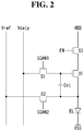
- FIG. 2 is a view showing a pixel circuit according to an exemplary embodiment of the present invention.
- the pixel circuit may comprise a light-emitting element EL, a driving TFT DT, a storage capacitor Cst, a first switching TFT S1, a second switching TFT S2, and a third switching TFT S3.
- the switching TFTs S1 to S3 and the driving TFT DT may be implemented as n-type MOSFETs.
- the light-emitting element EL comprises an organic compound layer situated between an anode and a cathode.
- the organic compound layer may consist of, but is not limited to, a hole injection layer (HIL), a hole transport layer (HTL), an emission layer (EML), an electron transport layer (ETL), and an electron injection layer (EIL).
- HIL hole injection layer
- HTL hole transport layer
- EML emission layer
- ETL electron transport layer
- EIL electron injection layer
- the cathode CAT of the light-emitting element EL is connected to the low-level power supply voltage VSS, and the anode ANO is connected to the source of the driving TFT DT.
- the driving TFT DT is a driving element that controls the current flowing through the light-emitting element EL in response to the gate-source voltage Vgs.
- the driving TFT DT comprises a gate connected to a second node node2, a source connected to a third node node3, and a drain connected to the first node node1.
- the second node node2 is connected to the gate of the driving TFT DT, one electrode of the storage capacitor Cst, and the source of the first switching TFT S1.
- the storage capacitor Cst is connected between the second node node2 and the third node node3.
- the high-level power supply voltage VDD is applied to the driving TFT DT via the first node node1.
- the input signal waveforms are as shown in FIG. 3 .
- FIG. 3 is a view of drive signal waveforms of the pixel circuit of FIG. 2 , which shows the waveforms of drive signals obtained when the characteristics of the driving TFT DT are compensated for in the first mode.
- "1H" represents 1 horizontal period in which data is written to the pixel.
- FIGS. 4A to 4C are views showing in steps how the pixel circuit of FIG. 2 works.
- first and second scan signals SCAN1 and SCAN2, an EM signal EM, and a data signal Vdata are applied. These signals SCAN1, SCAN2, and EM swing between high voltage and low voltage.
- the pixel circuit of FIG. 2 comprises n-type MOSFETS, for example, in which case the gate is on in the high-voltage state and off in the low-voltage state.
- the gate is turned on when the gate voltage is in the low-voltage state. Accordingly, in the description below, a voltage for turning on the gate is called the gate-on voltage, and a voltage for turning off the gate is called the gate-off voltage.
- the first scan signal SCAN1 is generated as the gate-on voltage during times t1 and t2 of 1 frame and generated as the gate-off voltage during time t3 and onwards.
- the second scan signal SCAN2 is generated as the gate-on voltage during time t1 and generated as the gate-off voltage during time t2 and onwards.
- the EM signal EM is generated as the gate-on voltage during times t1 and t2 and generated as the gate-off voltage during time t3 and onwards, or may switch on or off the pixels at a preset PWM (pulse width modulation) duty ratio.
- the first switching TFT S1 of FIG. 2 is turned on in response to the first scan signal SCAN1 during times t1 and t2 to supply a data voltage Vdata to the second node node2.
- the first switching TFT S1 comprises a gate connected to a first gate line to which the first scan signal SCAN1 is applied, a drain to which the data voltage Vdata is applied, and a source connected to the gate of the driving TFT DT via the second node node2.
- the second switching TFT S2 is turned on in response to the second scan signal SCAN2 to form a current path between a sensing line 13 and the first node node1 during time t1.
- the second switching TFT S2 comprises a gate connected to a second gate line to which the second scan signal SCAN2 is applied, a source to which a predetermined reference voltage Vref is applied, and a drain connected to the source of the driving TFT DT, the anode ANO of the light-emitting element EL, and the other electrode of the storage capacitor Cst via the third node node3.
- the reference voltage Vref is a voltage lower than the high-level power supply voltage VDD.
- the third switching TFT S3 is located between a VDD line and the drain of the driving TFT DT and switches the current path between the VDD line and the driving TFT DT in response to the EM signal EM.
- the third switching TFT S3 is turned on in response to the gate-on voltage of the EM signal EM during times t1 and t3 to supply the high-level power supply voltage VDD to the drain of the driving TFT DT via the first node node1.
- the third switching TFT S3 comprises a gate connected to a third gate line to which the EM signal EM is applied, a source connected to the drain of the driving TFT DT via the first node n1, and a drain to which the high-level power supply voltage VDD is applied via the VDD line.
- this pixel circuit will be described in steps with reference to FIGS. 4A to 4C .
- the switching TFTs S1, S2, and S3 are all turned on in response to the gate-on voltage of the first and second scan signals SCAN1 and SCAN2 and EM signal EM.
- the data voltage Vdata is applied to the second node node2.
- the voltage of the third node node3 is the reference voltage Vref
- the voltage of the first node node1 is reset to the high-level power supply voltage VDD.
- the driving TFT DT is turned on since the gate voltage is higher than the source voltage by threshold voltage Vth or above.
- the first switching TFT S1 remains in the on state since the first scan signal SCAN1 is held at the gate-on voltage, whereas the second switching TFT S2 is turned off since the second scan signal SCAN2 is inverted to the gate-off voltage.
- the current path of the pixel circuit is as shown in FIG. 4B .
- the third node node3 connected to the source of the driving TFT DT floats and the source voltage of the driving TFT DT varies with the characteristics of the driving TFT DT.
- the driving TFT DT has a large amount of current between the source and drain if it has high mobility during the real-time characteristics compensation time t2, which leads to a relatively large the source voltage and therefore makes Vgs relatively low.
- the driving TFT DT has a small amount of current between the source and drain if it has low mobility during the real-time characteristics compensation time t2, which leads to a relatively small amount of current discharged from the source voltage and therefore makes Vgs relatively higher.
- the brightness of the pixel is determined by the current in the light-emitting element EL which is proportional to Vgs of the driving TFT DT.
- a pixel A whose driving TFT DT has high mobility has a decrease in brightness because of a large reduction in Vgs of the driving TFT DT during the real-time characteristic compensation time t2
- a pixel whose driving TFT has relatively low mobility has less decrease in brightness because of a smaller reduction in Vgs of the driving TFT DT during the real-time characteristic compensation time t2.
- the above-described compensation process is performed in the first mode to compensate for variation in the characteristics of the driving TFT DT.
- characteristic compensation is performed for 1H period, and at the same time Vdata is applied.
- Vdata is applied.
- a voltage drop may occur because a current flows upon application of Vdata, and this may lead to a decrease in brightness.
- the second mode which enables brightness compensation, may be performed as well.
- FIG. 6 shows input signal waveforms obtained when brightness is compensated for in the second mode.
- "1H" represents 1 horizontal period in which data is written to the pixel.
- 1H period is divided into an initial period Tini and a data input period Tdata, and characteristic compensation is done in the initial period Tini of 1/2H and then Vdata is applied during the remaining 1/2H.
- first and second scan signals SCAN1 and SCAN2, an EM signal Em, and a data signal Vdata are applied. These signals SCAN1 and SCAN2, EM, and Vdata swing between high voltage and low voltage.
- the pixel circuit of FIG. 2 comprises n-type MOSFETS, for example, in which case the gate is on in the high-voltage state and off in the low-voltage state.
- the gate is turned on when the gate voltage is in the low-voltage state. Accordingly, in the description below, a voltage for turning on the gate is called the gate-on voltage, and a voltage for turning off the gate is called the gate-off voltage.
- the first scan signal SCAN1 is generated as the gate-on voltage and then the gate-off voltage in the initial period Tini of 1/2H and generated as the gate-on voltage and then the gate-off voltage in the data input period Tdata of 1/2H.
- the second scan signal SCAN2 is generated as the gate-on voltage during time t1 in the initial period Tini of 1/2H and generated as the gate-off voltage during time t2 and onwards.
- the EM signal EM is generated as the gate-on voltage during times t1 and t2 in the initial period Tini of 1/2H and generated as the gate-off voltage during time t3 and onwards.
- the EM signal EM is held at the gate-off voltage in the data input period Tdata of 1/2H and generated as the gate-on voltage after the end of the data input period Tdata.
- 1H period is divided into an initial period Tini and a data input period Tdata, and characteristic compensation is done in the initial period Tini of 1/2H and then data Vdata is applied during the remaining 1/2H.
- the EM signal is held at the gate-off voltage and data is applied while the light-emitting element EL is turned off.
- the data drive circuit 12 which supplies the data voltage Vdata has to comprise a component for supplying the initial voltage Vini and a component for supplying the data voltage Vdata.
- the pixel may operate in the initial period Tini of 1/2H, as explained with reference to FIGS. 4A to 4C .
- the switching TFTs S1, S2, and S3 are all turned on in response to the gate-on voltage of the first and second scan signals SCAN1 and SCAN2 and EM signal EM.
- the initial voltage Vini is applied to the second node node2.
- the voltage of the third node node3 is the reference voltage Vref
- the voltage of the first node node1 is reset to the high-level power supply voltage VDD.
- the driving TFT DT is turned on since the gate voltage is higher than the source voltage by threshold voltage Vth or above.
- the first switching TFT S1 remains in the on state since the first scan signal SCAN1 is held at the gate-on voltage, whereas the second switching TFT S2 is turned off since the second scan signal SCAN2 is inverted to the gate-off voltage.
- the current path of the pixel circuit is as shown in FIG. 4B .
- the third node node3 connected to the source of the driving TFT DT floats and the amount of current discharged from the source voltage of the driving TFT DT varies with the characteristics of the driving TFT DT.
- the driving TFT DT has a large amount of current between the source and drain if it has high mobility during the real-time characteristics compensation time t2, which leads to a relatively large amount of current discharged from the source voltage and therefore makes Vgs relatively low.
- the driving TFT DT has a small amount of current between the source and drain if it has low mobility during the real-time characteristics compensation time t2, which leads to a relatively small amount of current discharged from the source voltage and therefore makes Vgs relatively higher.
- the brightness of the pixel is determined by the current in the light-emitting element EL which is proportional to Vgs of the driving TFT DT.
- a pixel A whose driving TFT DT has high mobility has a decrease in brightness because of a large reduction in Vgs of the driving TFT DT during the real-time characteristic compensation time t2
- a pixel whose driving TFT has relatively low mobility has less decrease in brightness because of a smaller reduction in Vgs of the driving TFT DT during the real-time characteristic compensation time t2. Accordingly, variation in the characteristics of the driving TFT DT is compensated for across the entire screen, thus making the brightness of the pixels uniform across the entire screen.
- FIG. 7 shows how the pixel works in the data input period Tdata of 1/2H after the initial period Tini of 1/2H.
- the first scan signal SCAN1 is generated as the gate-on voltage and the second scan signal SCAN2 and the EM signal EM are generated as the gate-off voltage, thus turning on the first switching TFT S1 and turning off the other switching elements S2 and S3 and the light-emitting element EL.
- the data voltage Vdata is applied to the second node node2 through the turned-on first switching TFT S1. Since the second and third switching TFTs S2 and S3 and the light-emitting element EL are all turned off, the power supply line from the first node node1 to the third node node3 operates like a capacitor, and the data voltage Vdata is therefore written to the second node node2 of the driving TFT DT.
- VDD is supplied to the light-emitting element EL in response to Vgs of the driving TFT DT.
- 1H period is divided into an initial period Tini and a data input period Tdata, and characteristic compensation is done in the initial period Tini of 1/2H and then Vdata is applied during the remaining 1/2H. That is, data Vdata is written after characteristic compensation during 1H to allow the light-emitting element EL to emit light, thereby reducing the voltage drop to less than the threshold voltage Vth.
- FIGS. 8 and 9 show input signal waveforms applied to a pixel comprising p-type MOSFETs according to an exemplary embodiment of the present invention and how the pixel works.
- FIG. 8 is a waveform diagram of drive signals obtained when the pixel comprising p-type MOSFETs is controlled such that data Vdata is written after characteristic compensation during 1H to allow the light-emitting element EL to emit light.
- FIG. 9 shows how the pixel works in the data input period Tdata of FIG. 8 .
- inverted signal waveforms are obtained by inverting the waveforms of signals applied to a pixel comprising n-type MOSFETs.
- a voltage for turning on the gate of the p-type MOSFET is called the gate-on voltage
- a voltage for turning off the gate thereof is called the gate-off voltage.
- first and second scan signals SCAN1 and SCAN2, an EM signal EM, and a data signal Vdata are applied to the pixel. These signals SCAN1, SCAN2, and EM swing between high voltage and low voltage.
- "1H" represents 1 horizontal period in which data is written to the pixel.
- 1H period is divided into an initial period Tini and a data input period Tdata, and characteristic compensation is done in the initial period Tini of 1/2H and then Vdata is applied during the remaining 1/2H.
- the first scan signal SCAN1 is generated as the gate-on voltage and then the gate-off voltage in the initial period Tini of 1/2H and generated as the gate-on voltage and then the gate-off voltage in the data input period Tdata of 1/2H.
- the second scan signal SCAN2 is generated as the gate-on voltage and then the gate-off voltage in the initial period Tini of 1/2H and generated as the gate-on voltage and then the gate-off voltage in the data input period Tdata of 1/2H.
- the EM signal EM is generated as the gate-on voltage during times t1 in the initial period Tini of 1/2H and generated as the gate-off voltage during time t2 and onwards.
- the EM signal EM is held at the gate-off voltage in the data input period Tdata of 1/2H and generated as the gate-on voltage after the end of the data input period Tdata.
- 1H period is divided into an initial period Tini and a data input period Tdata, and the electrical characteristics are compensated for in the initial period Tini of 1/2H and then data Vdata is applied during the remaining 1/2H.
- the EM signal is held at the gate-off voltage and data is applied while the light-emitting element EL is turned off.
- the data drive circuit 12 which supplies the data voltage Vdata has to comprise a component for supplying the initial voltage Vini and a component for supplying the data voltage Vdata.
- the switching TFTs S1, S2, and S3 are all turned on in response to the gate-on voltage of the first and second scan signals SCAN1 and SCAN2 and EM signal EM.
- the initial voltage Vini is applied to the second node node2.
- the voltage of the third node node3 is the reference voltage Vref, and the voltage of the first node node1 is reset to the high-level power supply voltage VDD.
- the driving TFT DT is turned on since the gate voltage is higher than the source voltage by threshold voltage Vth or above.
- the first switching TFT S1 remains in the on state since the first scan signal SCAN1 is held at the gate-on voltage, whereas the second switching TFT S2 is turned off since the second scan signal SCAN2 is inverted to the gate-off voltage.
- the third node node3 connected to the source of the driving TFT DT floats and the amount of current discharged at the source voltage of the driving TFT DT varies with the characteristics of the driving TFT DT.
- the driving TFT DT has a large amount of current between the source and drain if it has high mobility during the real-time characteristics compensation time t2, which leads to a relatively large amount of current discharged at the source voltage and therefore makes Vgs relatively low.
- the driving TFT DT has a small amount of current between the source and drain if it has low mobility during the real-time characteristics compensation time t2, which leads to a relatively small amount of current discharged at the source voltage and therefore makes Vgs relatively higher.
- the brightness of the pixel is determined by the current in the light-emitting element EL which is proportional to Vgs of the driving TFT DT.
- a pixel A whose driving TFT DT has high mobility has a decrease in brightness because of a large reduction in Vgs of the driving TFT DT during the real-time characteristic compensation time t2
- a pixel whose driving TFT has relatively low mobility has less decrease in brightness because of a smaller reduction in Vgs of the driving TFT DT during the real-time characteristic compensation time t2. Accordingly, variation in the characteristics of the driving TFT DT is compensated for across the entire screen, thus making the brightness of the pixels uniform across the entire screen.
- the first scan signal SCAN1 is generated as the gate-on voltage and the second scan signal SCAN2 and the EM signal EM are generated as the gate-off voltage, thus turning on the first switching TFT S1 and turning off the other switching elements S2 and S3 and the light-emitting element EL.
- the data voltage Vdata is applied to the second node node2 through the turned-on first switching TFT S1. Since the second and third switching TFTs S2 and S3 and the light-emitting element EL are all turned off, the power supply line from the first node node1 to the third node node3 operates like a capacitor, and the data voltage Vdata is therefore written to the second node node2 of the driving TFT DT.
- VDD is supplied to the light-emitting element EL in response to Vgs of the driving TFT DT.
- 1H period is divided into an initial period Tini and a data input period Tdata, and characteristic compensation is done in the initial period Tini of 1/2H and then Vdata is applied during the remaining 1/2H. That is, data Vdata is written after characteristic compensation during 1H to allow the light-emitting element EL to emit light, thereby reducing the voltage drop to less than the threshold voltage Vth.
Landscapes
- Engineering & Computer Science (AREA)
- Physics & Mathematics (AREA)
- Computer Hardware Design (AREA)
- General Physics & Mathematics (AREA)
- Theoretical Computer Science (AREA)
- Microelectronics & Electronic Packaging (AREA)
- Control Of Indicators Other Than Cathode Ray Tubes (AREA)
- Control Of El Displays (AREA)
- Electroluminescent Light Sources (AREA)
Abstract
Description
- This application claims the benefit of Korean Patent Application No.,
10-2017-0083472 filed on June 30, 2017 - The present invention relates to an electroluminescence display and a method for driving the same.
- Electroluminescence displays are roughly classified into inorganic light-emitting displays and organic light-emitting displays depending on the material of an emission layer. Of these, an active-matrix organic light emitting display comprises organic light-emitting diodes (hereinafter, "OLED"), which are typical light-emitting diodes that emit light themselves, and has the advantages of fast response time, high luminous efficiency, high brightness, and wide viewing angle.
- An OLED of an organic light-emitting display comprises an anode, a cathode, and an organic compound layer situated between these electrodes. The organic compound layer consists of a hole injection layer (HIL), a hole transport layer (HTL), an emission layer (EML), an electron transport layer (ETL), and an electron injection layer (EIL). When a power voltage is applied to the anode and cathode, a hole passing through the hole transport layer HTL and an electron passing through the electron transport layer ETL move to the emission layer EML, forming an exciton. As a result, the emission layer EML generates visible light
- An organic light-emitting display has pixels arranged in a matrix, each pixel comprising an OLED and a driving TFT (thin film transistor), and adjusts the brightness of an image represented by pixels in accordance with the grayscale values of video data. The driving TFT controls the drive current flowing through the OLED in response to a voltage applied between its gate electrode and source electrode (hereinafter, "gate-source voltage"). The light intensity and brightness of the OLED are determined by the drive current.
- Generally, when the driving TFT operates in a saturation region, a drive current Ids flowing between the drain and source of the driving TFT is expressed as follows:

- The electrical characteristics of the pixels, such as the threshold voltage Vth of the driving TFT, the electron mobility µ of the driving TFT, and the threshold voltage of the OLED, should be the same for every pixel since they serve as a factor for determining the drive current Ids. However, the electrical characteristics may vary between pixels, due to various causes including process variation, temporal change, etc.
- To compensate for variation in the electrical characteristics of the driving TFT, internal compensation and external compensation may be applied. In the internal compensation method, variation in the electrical characteristics of the driving TFT between pixels is automatically compensated for in real time by using the gate-source voltage of the driving TFT which varies with the electrical characteristics of the driving TFT. In the external compensation method, variation in the electrical characteristics of the driving TFT between pixels is compensated for by sensing the voltage of each pixel varying with the electrical characteristics of the driving TFT and modulating data of an input image by an external circuit based on the sensed voltage.
- The present invention provides an electroluminescence display that compensates for variation in electrical characteristics such as the mobility, threshold voltage, etc. of the driving TFT and prevents brightness degradation that may occur when compensating for the electrical characteristics of the driving TFT.
- Various embodiments provide an electroluminescence display and a method for driving an electroluminescence display according to the independent claims. Further embodiments are described in the dependent claims. An exemplary embodiment of the present invention provides an electroluminescence display comprising a display panel where a plurality of pixels connected to a plurality of data lines and a plurality of gate lines are arranged, each pixel comprising: a driving TFT that controls the current in a light-emitting element EL in response to a data voltage applied to a gate; and switching TFTs that supply a high-level power supply voltage to the driving TFT in response to a gate-on voltage of an emission signal and control signals applied to the source and drain of the driving TFT, wherein the electroluminescence display switches between first and second modes, the first mode being a mode in which data writing and driving TFT characteristic compensation are performed within 1 horizontal period by applying a data voltage to the gate of the driving TFT, and the second mode being a mode in which data writing is performed within the 1 horizontal period by applying an initial voltage to the gate of the driving TFT and applying the data voltage upon completion of the compensation of the driving TFT characteristics.
- In one or more embodiments, each pixel comprises a driving TFT that controls the current in the light-emitting element by a gate-source voltage, a first switching TFT that applies a first voltage to the gate of the driving TFT in response to a first scan signal, a second switching TFT that applies a second voltage to the source of the driving TFT in response to a second scan signal, and a third switching TFT that supplies the high-level power supply voltage to the drain of the driving TFT in response to an emission signal, and the electroluminescence display further comprises: a gate drive circuit that generates the scan signals and the emission signal; and a data drive circuit that generates the initial voltage and a data voltage.
- In one or more embodiments, in the first mode, a data voltage is applied to the gate of the driving TFT within the 1 horizontal period while the first switching TFT, second switching TFT, and third switching TFT are turned on, and then the electrical characteristics of the driving TFT are compensated for while only the second switching TFT is turned off.
- In one or more embodiments, in the second mode, the initial voltage is applied to the gate of the driving TFT in an initial period of the 1 horizontal period while the first switching TFT and the third switching TFT are turned on and the second switching is turned off, and the data voltage is applied to the gate of the driving TFT in the remaining period of the 1 horizontal period while the second switching TFT and the third switching TFT are turned off and the first switching TFT is turned on.
- In one or more embodiments, in the second mode, the light-emitting element remains in the off state while the data voltage is applied to the gate of the driving TFT
- In one or more embodiments, during a compensation period for compensating for the characteristics of the driving TFT, the driving TFT is diode-connected by short-circuiting of the gate node and the drain node, and the potential of the gate node is fixed and the potential of the source node differs depending on the characteristics of the driving TFT.
- In one or more embodiments, in the first mode, the data drive circuit applies the data voltage to the gate node of the driving TFT through the first switching TFT within the 1 horizontal period.
- In one or more embodiments, in the second mode, the data drive circuit supplies the initial voltage to the data lines in an initial period of the 1 horizontal period and supplies the data voltage to the data lines in the remaining period of the 1 horizontal period.
- Another exemplary embodiment of the present invention provides a method for driving an electroluminescence display comprising a display panel where a plurality of pixels connected to a plurality of data lines and a plurality of gate lines are arranged, each pixel comprising: a driving TFT that controls the current in a light-emitting element EL in response to a data voltage applied to a gate; and switching TFTs that supply a high-level power supply voltage to the driving TFT in response to a gate-on voltage of an emission signal and control signals applied to the source and drain of the driving TFT, wherein the electroluminescence display switches between first and second modes, and the method comprises: operating the electroluminescence display in the first mode to perform data writing and driving TFT characteristic compensation within 1 horizontal period by applying a data voltage to the gate of the driving TFT; and operating the electroluminescence display in the second mode to perform data writing within the 1 horizontal period by applying an initial voltage to the gate of the driving TFT and applying the data voltage upon completion of the compensation of the driving TFT characteristics. Embodiments described herein for the electroluminescence display may similarly be applied to the method for driving an electroluminescence display.
- An electroluminescence display according to the present invention can compensate for the characteristics of the driving TFT of each pixel and prevent a decrease in brightness caused by voltage drop.
- An electroluminescence display according to the present invention allows for providing brightness uniformity and preventing a decrease in the brightness of the electroluminescence display, which may occur with characteristic compensation, since a data voltage is applied after the characteristics of the driving TFT are compensated for within 1 horizontal period.
- Furthermore, an electroluminescence display according to the present invention can minimize voltage loss, which may occur with driving TFT compensation, by writing a data voltage after characteristic compensation is completed.
- The accompanying drawings, which are included to provide a further understanding of the invention and are incorporated in and constitute a part of this specification, illustrate embodiments of the invention and together with the description serve to explain the principles of the invention. In the drawings:
-
FIG. 1 is a block diagram showing an electroluminescence display according to an exemplary embodiment of the present invention; -
FIG. 2 is a circuit diagram showing an example pixel circuit; -
FIG. 3 is a waveform diagram showing drive signal waveforms of a pixel circuit according to an exemplary embodiment of the present invention; -
FIGS. 4A to 4C are views showing in steps how the pixel circuit ofFIG. 2 works; -
FIG. 5 is a graph showing how brightness is made uniform by compensating for driving TFT characteristics; -
FIG. 6 is a waveform diagram showing drive signal waveforms of a pixel circuit according to another exemplary embodiment of the present invention; -
FIG. 7 is a view showing how the pixel circuit works in accordance with the signal waveforms ofFIG. 6 ; -
FIG. 8 is a waveform diagram showing drive signal waveforms of a pixel circuit according to yet another exemplary embodiment of the present invention; and -
FIG. 9 is a view showing how the pixel circuit works in accordance with the signal waveforms ofFIG. 8 . - Reference will now be made in detail to embodiments of the invention, examples of which are illustrated in the accompanying drawings.
- Various aspects and features of the present invention and methods of accomplishing them may be understood more readily by reference to the following detailed descriptions of exemplary embodiments and the accompanying drawings. The present invention may, however, be embodied in many different forms and should not be construed as being limited to the exemplary embodiments set forth herein. Rather, these exemplary embodiments are provided so that this disclosure will be thorough and complete and will fully convey the concept of the present invention to those skilled in the art, and the present invention is defined by the appended claims.
- The shapes, sizes, proportions, angles, numbers, etc. shown in the figures to describe the exemplary embodiments of the present invention are merely examples and not limited to those shown in the figures. Like reference numerals denote like elements throughout the specification. In describing the present invention, detailed descriptions of related well-known technologies will be omitted to avoid unnecessary obscuring the present invention. When the terms 'comprise', 'have', 'consist of' and the like are used, other parts may be added as long as the term 'only' is not used. The singular forms may be interpreted as the plural forms unless explicitly stated.
- The elements may be interpreted to include an error margin even if not explicitly stated.
- When the position relation between two parts is described using the terms "on", "over", "under", "next to" and the like, one or more parts may be positioned between the two parts as long as the term "immediately" or "directly" is not used.
- It will be understood that, although the terms "first", "second", etc. may be used herein to describe various elements, these elements are not limited by these terms. These terms are used to distinguish one element from another element. Thus, a first element mentioned below could also be termed as a second element without departing from the technical spirit of the present invention.
- Like reference numerals denote substantially like elements throughout the specification.
- The following exemplary embodiments of the present invention may be coupled or combined with one another either partly or wholly, and may technically interact or work together in various ways. The exemplary embodiments may be carried out independently or in connection with one another.
- In the present invention, pixel circuits and a gate driver which are formed on a substrate of a display panel may be implemented as n-type or p-type MOSFET (metal oxide semiconductor field effect transistor) TFTs. It should be noted that, although the exemplary embodiments below illustrate p-type TFTs (PMOS), the present invention is not limited to them. A TFT is a three-electrode device with gate, source, and drain. The source is an electrode that provides carriers to the transistor. The carriers in the TFT flow from the source. The drain is an electrode where the carriers leave the TFT. That is, in a MOSFET, carriers flow from the source to the drain. In the case of an n-type TFT (NMOS), the carriers are electrons, and thus the source voltage is lower than the drain voltage so that the electrons flow from the source to the drain. In the n-type TFT, since the electrons flow from the source to the drain, current flows from the drain to the source. In the case of a p-type TFT (PMOS), the carriers are holes, and thus the source voltage is higher than the drain voltage so that the holes flow from the source to the drain. In the p-type TFT, since the holes flow from the source to the drain, current flows from the source to the drain. It should be noted that the source and drain of a MOSFET are not fixed in position. For example, the source and drain of the MOSFET are interchangeable depending on the applied voltage.
- In what follows, gate-on voltage is the voltage of a gate signal by which a TFT is turned on, and gate-off voltage is a voltage by which the TFT is turned off. In PMOS, the gate-on voltage is a low voltage L, and the gate-off voltage is a high voltage H. In NMOS, the gate-on voltage is a high voltage H, and the gate-off voltage is a low voltage L.
- Hereinafter, various exemplary embodiments of the present invention will be described in detail with reference to the accompanying drawings. In the exemplary embodiments below, the description of the electroluminescence display will focus on an organic light-emitting display comprising organic light-emitting material. However, it should be noted that the technical idea of the present invention is not limited to organic light-emitting displays but may apply to inorganic light-emitting displays comprising inorganic light-emitting material.
-
FIG. 1 shows an electroluminescence display according to an exemplary embodiment of the present invention. - Referring to
FIG. 1 , the electroluminescence display according to the exemplary embodiment of the present invention comprises adisplay panel 10 with pixels PXL, adata drive circuit 12 for driving a plurality ofdata lines 14, agate drive circuit 13 for driving a plurality ofgate lines 15, and atiming controller 11 for controlling the operation timings of the data drivecircuit 12 andgate drive circuit 13. - The data lines 14 and the gate lines 15 intersect on the
display panel 10, and the pixels PXL are arranged in a matrix and located at the intersections. Pixels PXL in a row are connected to asingle gate line 15, and thisgate line 15 may comprise at least one scan line and at least one emission line. That is, each pixel PXL may be connected to asingle data line 14, at least one scan line, and at least one emission line. The pixels PXL may be commonly supplied with high-level and low-level operating voltages VDD and VSS and an initial voltage Vini from a power generator (not shown). To prevent unnecessary light emission from the OLED in an initial period and a sampling period, the initial voltage Vini may be preferably selected within a voltage range sufficiently lower than the operating voltage of the OLED, and may be set equal to or lower than the low-level operating voltage ELVSS. - The TFTs constituting the pixel PXL may be implemented as oxide TFTs each comprising an oxide semiconductor layer. When electron mobility, process deviation, etc. are all considered, the oxide TFTs are advantageous for a large-
sized display panel 10. However, the present invention is not limited thereto, but the semiconductor layers of the TFTs may be formed of amorphous silicon, polysilicon, etc. Each pixel PXL comprises a plurality of TFTs and a storage capacitor, in order to compensate for variation in the threshold voltage of the driving TFT. The present invention proposes a method for solving the problem of brightness degradation which occurs as compensation time increases. - The
timing controller 11 re-aligns digital video data RGB input from an external system board to match the resolution of thedisplay panel 10 and supplies it to the data drivecircuit 12. Also, thetiming controller 11 generates a data timing control signal DDC for controlling the operating timing of the data drivecircuit 12 and a gate timing control signal GDC for controlling the operating timing of thegate drive circuit 13, based on timing signals such as a vertical synchronization signal Vsync, a horizontal synchronization signal Hsync, a dot clock signal DCL, and a data enable signal DE. - The data drive
circuit 12 converts the digital video data RGB input from thetiming controller 11 to an analog data voltage based on the data control signal DDC. - The
gate drive circuit 13 generates a scan signal and an emission signal based on the gate control signal GDC. Thegate drive circuit 13 may comprise a scan driver and an emission driver. In order to drive at least one scan line connected to each pixel row, the scan driver may generate a scan signal and provide it to the scan lines on a line-sequential basis. In order to drive at least one emission line connected to each pixel row, the emission driver may generate an emission signal and provide it to the emission lines. - The electroluminescence display of the invention may provide first and second modes for compensating for the electrical characteristics of the driving TFT. The first and second modes are for compensating for the characteristics of the driving TFT. The first mode is a mode in which data writing and driving TFT characteristic compensation are performed simultaneously within 1
horizontal period 1H, and the second mode is a mode in which driving TFT characteristic compensation and data writing are sequentially performed within 1horizontal period 1H. Compared with the first mode, the second mode allows for compensating for a decrease in the brightness of the display panel caused by first mode operation by minimizing voltage drop. The electroluminescence display of the invention may be designed to switch between the first and second modes at given intervals or to perform compensation in the first mode or second mode depending on the driving condition of the display device. - In the electroluminescence display of the invention, as shown in
FIG. 2 , each subpixel comprises a driving TFT DT that controls the current in a light-emitting element EL by a gate-source voltage Vgs, and a switching TFT S3 that supplies a high-level power supply voltage VDD to the driving TFT DT in response to the gate-on voltage of an EM signal EM. - In this regard, the timing controller 21 may set a compensation time for compensating for the characteristics of the driving TFT DT within 1
horizontal period 1H according to the first mode or second mode, and generate a data control signal DDC and a gate control signal GDC by allowing a source node of the driving TFT to float and compensating for the characteristic of the driving TFT DT between the pixels P during the real-time characteristic compensation time. -
FIG. 2 is a view showing a pixel circuit according to an exemplary embodiment of the present invention. - Referring to
FIG. 2 , the pixel circuit may comprise a light-emitting element EL, a driving TFT DT, a storage capacitor Cst, a first switching TFT S1, a second switching TFT S2, and a third switching TFT S3. The switching TFTs S1 to S3 and the driving TFT DT may be implemented as n-type MOSFETs. - The light-emitting element EL comprises an organic compound layer situated between an anode and a cathode. The organic compound layer may consist of, but is not limited to, a hole injection layer (HIL), a hole transport layer (HTL), an emission layer (EML), an electron transport layer (ETL), and an electron injection layer (EIL). The cathode CAT of the light-emitting element EL is connected to the low-level power supply voltage VSS, and the anode ANO is connected to the source of the driving TFT DT.
- The driving TFT DT is a driving element that controls the current flowing through the light-emitting element EL in response to the gate-source voltage Vgs. The driving TFT DT comprises a gate connected to a second node node2, a source connected to a third node node3, and a drain connected to the first node node1. The second node node2 is connected to the gate of the driving TFT DT, one electrode of the storage capacitor Cst, and the source of the first switching TFT S1. The storage capacitor Cst is connected between the second node node2 and the third node node3. The high-level power supply voltage VDD is applied to the driving TFT DT via the first node node1.
- In this pixel circuit, when the characteristics of the driving TFT DT are compensated for in the first mode, the input signal waveforms are as shown in
FIG. 3 . -
FIG. 3 is a view of drive signal waveforms of the pixel circuit ofFIG. 2 , which shows the waveforms of drive signals obtained when the characteristics of the driving TFT DT are compensated for in the first mode. InFIG. 3 , "1H" represents 1 horizontal period in which data is written to the pixel.FIGS. 4A to 4C are views showing in steps how the pixel circuit ofFIG. 2 works. - As shown in
FIG. 3 , first and second scan signals SCAN1 and SCAN2, an EM signal EM, and a data signal Vdata are applied. These signals SCAN1, SCAN2, and EM swing between high voltage and low voltage. The pixel circuit ofFIG. 2 comprises n-type MOSFETS, for example, in which case the gate is on in the high-voltage state and off in the low-voltage state. On the other hand, in a case where the pixel circuit comprises p-type MOSFETs, the gate is turned on when the gate voltage is in the low-voltage state. Accordingly, in the description below, a voltage for turning on the gate is called the gate-on voltage, and a voltage for turning off the gate is called the gate-off voltage. - The first scan signal SCAN1 is generated as the gate-on voltage during times t1 and t2 of 1 frame and generated as the gate-off voltage during time t3 and onwards.
- The second scan signal SCAN2 is generated as the gate-on voltage during time t1 and generated as the gate-off voltage during time t2 and onwards. The EM signal EM is generated as the gate-on voltage during times t1 and t2 and generated as the gate-off voltage during time t3 and onwards, or may switch on or off the pixels at a preset PWM (pulse width modulation) duty ratio.
- According to the signal waveforms of
FIG. 3 , the first switching TFT S1 ofFIG. 2 is turned on in response to the first scan signal SCAN1 during times t1 and t2 to supply a data voltage Vdata to the second node node2. The first switching TFT S1 comprises a gate connected to a first gate line to which the first scan signal SCAN1 is applied, a drain to which the data voltage Vdata is applied, and a source connected to the gate of the driving TFT DT via the second node node2. - The second switching TFT S2 is turned on in response to the second scan signal SCAN2 to form a current path between a
sensing line 13 and the first node node1 during time t1. The second switching TFT S2 comprises a gate connected to a second gate line to which the second scan signal SCAN2 is applied, a source to which a predetermined reference voltage Vref is applied, and a drain connected to the source of the driving TFT DT, the anode ANO of the light-emitting element EL, and the other electrode of the storage capacitor Cst via the third node node3. The reference voltage Vref is a voltage lower than the high-level power supply voltage VDD. - The third switching TFT S3 is located between a VDD line and the drain of the driving TFT DT and switches the current path between the VDD line and the driving TFT DT in response to the EM signal EM. The third switching TFT S3 is turned on in response to the gate-on voltage of the EM signal EM during times t1 and t3 to supply the high-level power supply voltage VDD to the drain of the driving TFT DT via the first node node1. The third switching TFT S3 comprises a gate connected to a third gate line to which the EM signal EM is applied, a source connected to the drain of the driving TFT DT via the first node n1, and a drain to which the high-level power supply voltage VDD is applied via the VDD line.
- The operation of this pixel circuit will be described in steps with reference to
FIGS. 4A to 4C . - During the reset time t1, the switching TFTs S1, S2, and S3 are all turned on in response to the gate-on voltage of the first and second scan signals SCAN1 and SCAN2 and EM signal EM. In this case, as shown in
FIG. 4A , the data voltage Vdata is applied to the second node node2. During the reset time t1, the voltage of the third node node3 is the reference voltage Vref, and the voltage of the first node node1 is reset to the high-level power supply voltage VDD. During the reset time t1, the driving TFT DT is turned on since the gate voltage is higher than the source voltage by threshold voltage Vth or above. - Next, during the real-time characteristic compensation time t2, the first switching TFT S1 remains in the on state since the first scan signal SCAN1 is held at the gate-on voltage, whereas the second switching TFT S2 is turned off since the second scan signal SCAN2 is inverted to the gate-off voltage. In this case, the current path of the pixel circuit is as shown in
FIG. 4B . During the real-time characteristic compensation time t2, the third node node3 connected to the source of the driving TFT DT floats and the source voltage of the driving TFT DT varies with the characteristics of the driving TFT DT. - The driving TFT DT has a large amount of current between the source and drain if it has high mobility during the real-time characteristics compensation time t2, which leads to a relatively large the source voltage and therefore makes Vgs relatively low. On the other hand, the driving TFT DT has a small amount of current between the source and drain if it has low mobility during the real-time characteristics compensation time t2, which leads to a relatively small amount of current discharged from the source voltage and therefore makes Vgs relatively higher. The brightness of the pixel is determined by the current in the light-emitting element EL which is proportional to Vgs of the driving TFT DT. Thus, a pixel A whose driving TFT DT has high mobility has a decrease in brightness because of a large reduction in Vgs of the driving TFT DT during the real-time characteristic compensation time t2, whereas a pixel whose driving TFT has relatively low mobility has less decrease in brightness because of a smaller reduction in Vgs of the driving TFT DT during the real-time characteristic compensation time t2.
- Accordingly, as can be seen from the pixel brightness before and after compensation in
FIG. 5 , variation in the characteristics of the driving TFT DT is compensated for across the entire screen, thus making the brightness of the pixels uniform across the entire screen - The above-described compensation process is performed in the first mode to compensate for variation in the characteristics of the driving TFT DT. In the first mode, characteristic compensation is performed for 1H period, and at the same time Vdata is applied. Thus, a voltage drop may occur because a current flows upon application of Vdata, and this may lead to a decrease in brightness. Due to this, in the present invention, the second mode, which enables brightness compensation, may be performed as well.
-
FIG. 6 shows input signal waveforms obtained when brightness is compensated for in the second mode. InFIG. 6 , "1H" represents 1 horizontal period in which data is written to the pixel. In the case of compensation in the second mode, 1H period is divided into an initial period Tini and a data input period Tdata, and characteristic compensation is done in the initial period Tini of 1/2H and then Vdata is applied during the remaining 1/2H. - As shown in
FIG. 6 , first and second scan signals SCAN1 and SCAN2, an EM signal Em, and a data signal Vdata are applied. These signals SCAN1 and SCAN2, EM, and Vdata swing between high voltage and low voltage. The pixel circuit ofFIG. 2 comprises n-type MOSFETS, for example, in which case the gate is on in the high-voltage state and off in the low-voltage state. On the other hand, in a case where the pixel circuit comprises p-type MOSFETs, the gate is turned on when the gate voltage is in the low-voltage state. Accordingly, in the description below, a voltage for turning on the gate is called the gate-on voltage, and a voltage for turning off the gate is called the gate-off voltage. - The first scan signal SCAN1 is generated as the gate-on voltage and then the gate-off voltage in the initial period Tini of 1/2H and generated as the gate-on voltage and then the gate-off voltage in the data input period Tdata of 1/2H.
- The second scan signal SCAN2 is generated as the gate-on voltage during time t1 in the initial period Tini of 1/2H and generated as the gate-off voltage during time t2 and onwards.
- The EM signal EM is generated as the gate-on voltage during times t1 and t2 in the initial period Tini of 1/2H and generated as the gate-off voltage during time t3 and onwards. Thus, the EM signal EM is held at the gate-off voltage in the data input period Tdata of 1/2H and generated as the gate-on voltage after the end of the data input period Tdata.
- According to the signal waveforms of
FIG. 6 , 1H period is divided into an initial period Tini and a data input period Tdata, and characteristic compensation is done in the initial period Tini of 1/2H and then data Vdata is applied during the remaining 1/2H. In the data input period Tdata, the EM signal is held at the gate-off voltage and data is applied while the light-emitting element EL is turned off. Thus, the data drivecircuit 12 which supplies the data voltage Vdata has to comprise a component for supplying the initial voltage Vini and a component for supplying the data voltage Vdata. - Upon receiving the signals with the waveforms of
FIG. 6 , the pixel may operate in the initial period Tini of 1/2H, as explained with reference toFIGS. 4A to 4C . - During the reset time t1 of 1/2H, the switching TFTs S1, S2, and S3 are all turned on in response to the gate-on voltage of the first and second scan signals SCAN1 and SCAN2 and EM signal EM. In this case, as shown in
FIG. 4A , the initial voltage Vini is applied to the second node node2. During the reset time t1, the voltage of the third node node3 is the reference voltage Vref, and the voltage of the first node node1 is reset to the high-level power supply voltage VDD. During the reset time t1, the driving TFT DT is turned on since the gate voltage is higher than the source voltage by threshold voltage Vth or above. - Next, during the real-time characteristic compensation time t2, the first switching TFT S1 remains in the on state since the first scan signal SCAN1 is held at the gate-on voltage, whereas the second switching TFT S2 is turned off since the second scan signal SCAN2 is inverted to the gate-off voltage. In this case, the current path of the pixel circuit is as shown in
FIG. 4B . During the real-time characteristic compensation time t2, the third node node3 connected to the source of the driving TFT DT floats and the amount of current discharged from the source voltage of the driving TFT DT varies with the characteristics of the driving TFT DT. - The driving TFT DT has a large amount of current between the source and drain if it has high mobility during the real-time characteristics compensation time t2, which leads to a relatively large amount of current discharged from the source voltage and therefore makes Vgs relatively low. On the other hand, the driving TFT DT has a small amount of current between the source and drain if it has low mobility during the real-time characteristics compensation time t2, which leads to a relatively small amount of current discharged from the source voltage and therefore makes Vgs relatively higher. The brightness of the pixel is determined by the current in the light-emitting element EL which is proportional to Vgs of the driving TFT DT. Thus, a pixel A whose driving TFT DT has high mobility has a decrease in brightness because of a large reduction in Vgs of the driving TFT DT during the real-time characteristic compensation time t2, whereas a pixel whose driving TFT has relatively low mobility has less decrease in brightness because of a smaller reduction in Vgs of the driving TFT DT during the real-time characteristic compensation time t2. Accordingly, variation in the characteristics of the driving TFT DT is compensated for across the entire screen, thus making the brightness of the pixels uniform across the entire screen.
-
FIG. 7 shows how the pixel works in the data input period Tdata of 1/2H after the initial period Tini of 1/2H. - In the data input period Tdata, the first scan signal SCAN1 is generated as the gate-on voltage and the second scan signal SCAN2 and the EM signal EM are generated as the gate-off voltage, thus turning on the first switching TFT S1 and turning off the other switching elements S2 and S3 and the light-emitting element EL.
- Afterwards, as shown in
FIG. 7 , the data voltage Vdata is applied to the second node node2 through the turned-on first switching TFT S1. Since the second and third switching TFTs S2 and S3 and the light-emitting element EL are all turned off, the power supply line from the first node node1 to the third node node3 operates like a capacitor, and the data voltage Vdata is therefore written to the second node node2 of the driving TFT DT. - After time t4, when the first scan signal SCAN1 is inverted to the gate-off voltage and the EM signal EM is inverted to the gate-on voltage, VDD is supplied to the light-emitting element EL in response to Vgs of the driving TFT DT.
- As such, in the present invention, 1H period is divided into an initial period Tini and a data input period Tdata, and characteristic compensation is done in the initial period Tini of 1/2H and then Vdata is applied during the remaining 1/2H. That is, data Vdata is written after characteristic compensation during 1H to allow the light-emitting element EL to emit light, thereby reducing the voltage drop to less than the threshold voltage Vth.
- While the foregoing description has been given of a pixel comprising n-type MOSFETs, the present invention may also be applicable to a pixel comprising p-type MOSFETs.
-
FIGS. 8 and9 show input signal waveforms applied to a pixel comprising p-type MOSFETs according to an exemplary embodiment of the present invention and how the pixel works. -
FIG. 8 is a waveform diagram of drive signals obtained when the pixel comprising p-type MOSFETs is controlled such that data Vdata is written after characteristic compensation during 1H to allow the light-emitting element EL to emit light.FIG. 9 shows how the pixel works in the data input period Tdata ofFIG. 8 . - In the case of the p-type MOSFET, the gate is on in the low-voltage state and off in the high-voltage state. Thus, inverted signal waveforms are obtained by inverting the waveforms of signals applied to a pixel comprising n-type MOSFETs. In the description below, a voltage for turning on the gate of the p-type MOSFET is called the gate-on voltage, and a voltage for turning off the gate thereof is called the gate-off voltage.
- Referring to
FIG. 8 , first and second scan signals SCAN1 and SCAN2, an EM signal EM, and a data signal Vdata are applied to the pixel. These signals SCAN1, SCAN2, and EM swing between high voltage and low voltage. InFIG. 8 , "1H" represents 1 horizontal period in which data is written to the pixel. In the case of compensation in the second mode, 1H period is divided into an initial period Tini and a data input period Tdata, and characteristic compensation is done in the initial period Tini of 1/2H and then Vdata is applied during the remaining 1/2H. - The first scan signal SCAN1 is generated as the gate-on voltage and then the gate-off voltage in the initial period Tini of 1/2H and generated as the gate-on voltage and then the gate-off voltage in the data input period Tdata of 1/2H.
- The second scan signal SCAN2 is generated as the gate-on voltage and then the gate-off voltage in the initial period Tini of 1/2H and generated as the gate-on voltage and then the gate-off voltage in the data input period Tdata of 1/2H.
- The EM signal EM is generated as the gate-on voltage during times t1 in the initial period Tini of 1/2H and generated as the gate-off voltage during time t2 and onwards. Thus, the EM signal EM is held at the gate-off voltage in the data input period Tdata of 1/2H and generated as the gate-on voltage after the end of the data input period Tdata.
- According to the signal waveforms of
FIG. 8 , 1H period is divided into an initial period Tini and a data input period Tdata, and the electrical characteristics are compensated for in the initial period Tini of 1/2H and then data Vdata is applied during the remaining 1/2H. In the data input period Tdata, the EM signal is held at the gate-off voltage and data is applied while the light-emitting element EL is turned off. Thus, the data drivecircuit 12 which supplies the data voltage Vdata has to comprise a component for supplying the initial voltage Vini and a component for supplying the data voltage Vdata. - In the pixel circuit of
FIG. 9 , during the initial period of 1/2H, the switching TFTs S1, S2, and S3 are all turned on in response to the gate-on voltage of the first and second scan signals SCAN1 and SCAN2 and EM signal EM. In this case, the initial voltage Vini is applied to the second node node2. During the reset time t1, the voltage of the third node node3 is the reference voltage Vref, and the voltage of the first node node1 is reset to the high-level power supply voltage VDD. During the reset time t1, the driving TFT DT is turned on since the gate voltage is higher than the source voltage by threshold voltage Vth or above. - Next, during the real-time characteristic compensation time t2, the first switching TFT S1 remains in the on state since the first scan signal SCAN1 is held at the gate-on voltage, whereas the second switching TFT S2 is turned off since the second scan signal SCAN2 is inverted to the gate-off voltage. During the characteristic compensation time t2, the third node node3 connected to the source of the driving TFT DT floats and the amount of current discharged at the source voltage of the driving TFT DT varies with the characteristics of the driving TFT DT.
- The driving TFT DT has a large amount of current between the source and drain if it has high mobility during the real-time characteristics compensation time t2, which leads to a relatively large amount of current discharged at the source voltage and therefore makes Vgs relatively low. On the other hand, the driving TFT DT has a small amount of current between the source and drain if it has low mobility during the real-time characteristics compensation time t2, which leads to a relatively small amount of current discharged at the source voltage and therefore makes Vgs relatively higher. The brightness of the pixel is determined by the current in the light-emitting element EL which is proportional to Vgs of the driving TFT DT. Thus, a pixel A whose driving TFT DT has high mobility has a decrease in brightness because of a large reduction in Vgs of the driving TFT DT during the real-time characteristic compensation time t2, whereas a pixel whose driving TFT has relatively low mobility has less decrease in brightness because of a smaller reduction in Vgs of the driving TFT DT during the real-time characteristic compensation time t2. Accordingly, variation in the characteristics of the driving TFT DT is compensated for across the entire screen, thus making the brightness of the pixels uniform across the entire screen.
- In the data input period Tdata, as shown in
FIG. 9 , the first scan signal SCAN1 is generated as the gate-on voltage and the second scan signal SCAN2 and the EM signal EM are generated as the gate-off voltage, thus turning on the first switching TFT S1 and turning off the other switching elements S2 and S3 and the light-emitting element EL. - The data voltage Vdata is applied to the second node node2 through the turned-on first switching TFT S1. Since the second and third switching TFTs S2 and S3 and the light-emitting element EL are all turned off, the power supply line from the first node node1 to the third node node3 operates like a capacitor, and the data voltage Vdata is therefore written to the second node node2 of the driving TFT DT.
- After time t4, when the first scan signal SCAN1 is inverted to the gate-off voltage and the EM signal EM is inverted to the gate-on voltage, VDD is supplied to the light-emitting element EL in response to Vgs of the driving TFT DT.
- As such, in the present invention, 1H period is divided into an initial period Tini and a data input period Tdata, and characteristic compensation is done in the initial period Tini of 1/2H and then Vdata is applied during the remaining 1/2H. That is, data Vdata is written after characteristic compensation during 1H to allow the light-emitting element EL to emit light, thereby reducing the voltage drop to less than the threshold voltage Vth.
- From the foregoing description, those skilled in the art will readily appreciate that various changes and modifications can be made without departing from the technical idea of the present invention. Therefore, the technical scope of the present invention is not limited to what has been stated in the detailed description of the specification but defined by the appended claims.
Claims (14)
- An electroluminescence display comprising a display panel (10) where a plurality of pixels (PXL) connected to a plurality of data lines (14) and a plurality of gate lines (15) are arranged, each pixel (PXL) comprising:a driving thin film transistor (DT) that is configured to control the current in a light-emitting element (EL) in response to a data voltage (Vdata) applied to a gate of the driving thin film transistor (DT); andswitching thin film transistors (S1, S2, S3) that are configured to supply a high-level power supply voltage (VDD) to the driving thin film transistor (DT) in response to a gate-on voltage of an emission signal (EM) and control signals applied to the gate and source and of the driving thin film transistor (DT),wherein the electroluminescence display is configured to switch between first and second modes, the first mode being a mode in which data writing and driving thin film transistor characteristics compensation are performed within 1 horizontal period (1H) by applying the data voltage (Vdata) to the gate of the driving thin film transistor (DT), and the second mode being a mode in which data writing is performed within the 1 horizontal period (1H) by applying an initial voltage (Vini) to the gate of the driving thin film transistor (DT) and applying the data voltage (Vdata) upon completion of the compensation of the driving thin film transistor characteristics.
- The electroluminescence display of claim 1, wherein each pixel (PXL) comprises the driving thin film transistor (DT) that is configured to control the current in the light-emitting element (EL) by a gate-source voltage, a first switching thin film transistor (S1) that is configured to apply a first voltage to the gate of the driving thin film transistor (DT) in response to a first scan signal (SCAN1), a second switching thin film transistor (S2) that is configured to apply a second voltage to the source of the driving thin film transistor (DT) in response to a second scan signal (SCAN2), and a third switching thin film transistor (S3) that supplies the high-level power supply voltage (VDD) to the drain of the driving thin film transistor (DT) in response to the emission signal (EM), and the electroluminescence display further comprises:a gate drive circuit (13) that is configured to generate the scan signals (SCAN1, SCAN2) and the emission signal (EM); anda data drive circuit (12) that is configured to generate the initial voltage (Vini) and the data voltage (Vdata).
- The electroluminescence display of claim 2, configured such that, in the first mode, the data voltage (Vdata) is applied to the gate of the driving thin film transistor (DT) within the 1 horizontal period (1H) while the first switching thin film transistor (S1), second switching thin film transistor (S2), and third switching thin film transistor (S3) are turned on, and then the electrical characteristics of the driving thin film transistor (DT) are compensated for while only the second switching thin film transistor (S2) is turned off.
- The electroluminescence display of claim 2 or 3, configured such that, in the second mode, the initial voltage (Vini) is applied to the gate of the driving thin film transistor (DT) in an initial period of the 1 horizontal period (1H) while the first switching thin film transistor (S1) and the third switching thin film transistor (S3) are turned on and the second switching thin film transistor (S2) is turned off, and the data voltage (Vdata) is applied to the gate of the driving thin film transistor (DT) in the remaining period of the 1 horizontal period (1H) while the second switching thin film transistor (S2) and the third switching thin film transistor (S3) are turned off and the first switching thin film transistor (S1) is turned on.
- The electroluminescence display of any one of claims 2 to 4, configured such that, in the second mode, the light-emitting element (EL) remains in the off state while the data voltage (Vdata) is applied to the gate of the driving thin film transistor (DT).
- The electroluminescence display of any one of claims 2 to 5, configured such that, during a compensation period for compensating for the characteristics of the driving thin film transistor (DT), the driving thin film transistor (DT) is diode-connected by short-circuiting of the gate and the drain of the driving thin film transistor (DT), and the potential of the gate is fixed and the potential of the source differs depending on the characteristics of the driving thin film transistor (DT).
- The electroluminescence display of any one of claims 2 to 6, configured such that, in the first mode, the data drive circuit (12) applies the data voltage (Vdata) to the gate of the driving thin film transistor (DT) through the first switching thin film transistor (S1) within the 1 horizontal period (1H).
- The electroluminescence display of claim 2 or 3, configured such that, in the second mode, the data drive circuit (12) supplies the initial voltage (Vini) to the data lines (14) in an initial period of the 1 horizontal period (1H) and supplies the data voltage (Vdata) to the data lines (14) in the remaining period of the 1 horizontal period (1H).
- A method for driving an electroluminescence display comprising a display panel (10) where a plurality of pixels (PXL) connected to a plurality of data lines (14) and a plurality of gate lines (15) are arranged, each pixel (PXL) comprising:a driving thin film transistor (DT) that controls the current in a light-emitting element (EL) in response to a data voltage (Vdata) applied to a gate of the driving thin film transistor (DT); andswitching thin film transistors (S1, S2, S3) that supply a high-level power supply voltage (VDD) to the driving thin film transistor (DT) in response to a gate-on voltage of an emission signal (EM) and control signals applied to the gate and source of the driving thin film transistor (DT),wherein the electroluminescence display switches between first and second modes, and the method comprises:operating the electroluminescence display in the first mode to perform data writing and driving thin film transistor characteristics compensation within 1 horizontal period (1H) by applying a data voltage (Vdata) to the gate of the driving thin film transistor (DT); andoperating the electroluminescence display in the second mode to perform data writing within the 1 horizontal period (1H) by applying an initial voltage (Vini) to the gate of the driving thin film transistor (DT) and applying the data voltage (Vdata) upon completion of the compensation of the driving thin film transistor characteristics.
- The method of claim 9, wherein each pixel (PXL) comprises a driving thin film transistor (DT) that controls the current in the light-emitting element (EL) by a gate-source voltage, a first switching thin film transistor (S1) that applies a first voltage to the gate of the driving thin film transistor (DT) in response to a first scan signal (S1), a second switching thin film transistor (S2) that applies a second voltage to the source of the driving thin film transistor (DT) in response to a second scan signal (S2), and a third switching thin film transistor (S3) that supplies the high-level power supply voltage (VDD) to the drain of the driving thin film transistor (DT) in response to an emission signal (EM), and the electroluminescence display further comprises:a gate drive circuit (13) that generates the scan signals (SCAN1, SCAN2) and the emission signal (EM); anda data drive circuit (12) that generates the initial voltage (Vini) and a data voltage (Vdata).
- The method of claim 10, wherein, in the first mode, a data voltage (Vdata) is applied to the gate of the driving thin film transistor (DT) within the 1 horizontal period (1H) while the first switching thin film transistor (S1), second switching thin film transistor (S2), and third switching thin film transistor (S3) are turned on, and then the electrical characteristics of the driving thin film transistor (DT) are compensated for while only the second switching thin film transistor (S2) is turned off.
- The method of claim 10 or 11, wherein, in the second mode, the initial voltage (Vini) is applied to the gate of the driving thin film transistor (DT) in an initial period of the 1 horizontal period (1H) while the first switching thin film transistor (S1) and the third switching thin film transistor (S3) are turned on and the second switching thin film transistor (S2) is turned off, and the data voltage (Vdata) is applied to the gate of the driving thin film transistor (DT) in the remaining period of the 1 horizontal period (1H) while the second switching thin film transistor (S2) and the third switching thin film transistor (S3) are turned off and the first switching thin film transistor (S1) is turned on.
- The method of any one of claims 10 to 12, wherein, in the second mode, the light-emitting element (EL) remains in the off state while the data voltage (Vdata) is applied to the gate of the driving thin film transistor (DT).
- The method of any one of claims 10 to 13, wherein, during a compensation period for compensating for the characteristics of the driving thin film transistor (DT), the driving thin film transistor (DT) is diode-connected by short-circuiting of the gate and the drain of the driving thin film transistor (DT), and the potential of the gate node is fixed and the potential of the source node differs depending on the characteristics of the driving thin film transistor (DT).
Applications Claiming Priority (1)
| Application Number | Priority Date | Filing Date | Title |
|---|---|---|---|
| KR1020170083472A KR102326166B1 (en) | 2017-06-30 | 2017-06-30 | Electroluminescent Display Device and Driving Method thereof |
Publications (1)
| Publication Number | Publication Date |
|---|---|
| EP3422335A1 true EP3422335A1 (en) | 2019-01-02 |
Family
ID=62562970
Family Applications (1)
| Application Number | Title | Priority Date | Filing Date |
|---|---|---|---|
| EP18176258.4A Ceased EP3422335A1 (en) | 2017-06-30 | 2018-06-06 | Electroluminescence display and method for driving the same |
Country Status (4)
| Country | Link |
|---|---|
| US (1) | US11075257B2 (en) |
| EP (1) | EP3422335A1 (en) |
| KR (1) | KR102326166B1 (en) |
| CN (1) | CN109215579B (en) |
Families Citing this family (13)
| Publication number | Priority date | Publication date | Assignee | Title |
|---|---|---|---|---|
| KR102372054B1 (en) * | 2017-09-05 | 2022-03-11 | 삼성디스플레이 주식회사 | Display device and pixel |
| US11430404B2 (en) * | 2018-05-25 | 2022-08-30 | Semiconductor Energy Laboratory Co., Ltd. | Display device including pixel and electronic device |
| KR102661852B1 (en) | 2018-08-13 | 2024-04-30 | 삼성디스플레이 주식회사 | Display device performing a sensing operation |
| US11004398B2 (en) * | 2018-11-20 | 2021-05-11 | Innolux Corporation | Electronic device |
| KR102632445B1 (en) * | 2019-01-15 | 2024-02-01 | 삼성디스플레이 주식회사 | Organic light emitting diode display device and manufacturing method thereof |
| CN109686304B (en) * | 2019-02-20 | 2020-09-01 | 深圳市华星光电半导体显示技术有限公司 | Display panel and driving method thereof |
| CN109979378B (en) * | 2019-05-15 | 2020-12-04 | 京东方科技集团股份有限公司 | Pixel drive circuit and display panel |
| KR20210027110A (en) | 2019-08-29 | 2021-03-10 | 가부시키가이샤 한도오따이 에네루기 켄큐쇼 | Display device |
| KR102729886B1 (en) * | 2019-12-26 | 2024-11-13 | 엘지디스플레이 주식회사 | Pixel circuit, electroluminescent display using the same, and method for sensing chracteristic of light emission control transistor using the same |
| CN114267640B (en) * | 2020-09-16 | 2024-10-25 | 长鑫存储技术有限公司 | Semiconductor device and method for manufacturing the same |
| TWI747647B (en) * | 2020-12-07 | 2021-11-21 | 友達光電股份有限公司 | Display device and pixel driving circuit |
| KR102774884B1 (en) * | 2020-12-17 | 2025-03-04 | 엘지디스플레이 주식회사 | Electroluminescence Display Device And Driving Method Of The Same |
| CN119132227B (en) * | 2024-10-29 | 2025-10-10 | 武汉华星光电技术有限公司 | Display driving device, driving method and display panel |
Citations (3)
| Publication number | Priority date | Publication date | Assignee | Title |
|---|---|---|---|---|
| US20080218452A1 (en) * | 2007-03-09 | 2008-09-11 | Hitachi Displays, Ltd. | Image display apparatus |
| US20110074757A1 (en) * | 2009-09-30 | 2011-03-31 | Bo-Yong Chung | Pixel circuit and organic electroluminescent display including the same |
| US20160171930A1 (en) * | 2014-12-10 | 2016-06-16 | Lg Display Co., Ltd. | Organic light emitting diode display device |
Family Cites Families (19)
| Publication number | Priority date | Publication date | Assignee | Title |
|---|---|---|---|---|
| JP4115763B2 (en) * | 2002-07-10 | 2008-07-09 | パイオニア株式会社 | Display device and display method |
| US7161566B2 (en) * | 2003-01-31 | 2007-01-09 | Eastman Kodak Company | OLED display with aging compensation |
| US7224332B2 (en) * | 2003-11-25 | 2007-05-29 | Eastman Kodak Company | Method of aging compensation in an OLED display |
| US6995519B2 (en) * | 2003-11-25 | 2006-02-07 | Eastman Kodak Company | OLED display with aging compensation |
| JP6099300B2 (en) * | 2011-09-13 | 2017-03-22 | 三星ディスプレイ株式會社Samsung Display Co.,Ltd. | Pixel circuit and display device |
| JP2014115543A (en) * | 2012-12-11 | 2014-06-26 | Samsung Display Co Ltd | Display device and method of driving pixel circuit thereof |
| KR102059368B1 (en) * | 2013-12-18 | 2019-12-26 | 엘지디스플레이 주식회사 | Organic light emitting display device with compensation function |
| KR102286641B1 (en) * | 2014-09-11 | 2021-08-06 | 엘지디스플레이 주식회사 | Organic Light Emitting Display Compensating For A Luminance Variation Due To The Change With Time Of The Drive Element |
| KR102320311B1 (en) | 2014-12-02 | 2021-11-02 | 삼성디스플레이 주식회사 | Organic light emitting display and driving method of the same |
| KR102459703B1 (en) * | 2014-12-29 | 2022-10-27 | 엘지디스플레이 주식회사 | Organic light emitting diode display and drving method thereof |
| CN105989796B (en) * | 2015-02-05 | 2019-08-30 | 群创光电股份有限公司 | Organic light emitting diode display panel with threshold voltage compensation and driving method |
| KR102475425B1 (en) * | 2015-07-21 | 2022-12-09 | 삼성디스플레이 주식회사 | Pixel, driving method of the pixel and organic light emittng display device including the pixel |
| KR102411075B1 (en) * | 2015-08-24 | 2022-06-21 | 삼성디스플레이 주식회사 | Pixel and organic light emitting display device having the same |
| KR102339649B1 (en) * | 2015-08-31 | 2021-12-16 | 엘지디스플레이 주식회사 | Organic Light Emitting Display and Method of Driving the same |
| KR102368078B1 (en) | 2015-08-31 | 2022-02-28 | 엘지디스플레이 주식회사 | Organic light emitting display device and method for driving the same |
| KR102509240B1 (en) * | 2015-11-30 | 2023-03-13 | 엘지디스플레이 주식회사 | Display Device |
| CN106782320B (en) * | 2016-12-29 | 2019-02-19 | 深圳市华星光电技术有限公司 | The threshold voltage method for detecting of OLED driving thin film transistor (TFT) |
| CN106652911B (en) * | 2017-02-24 | 2019-03-12 | 深圳市华星光电半导体显示技术有限公司 | OLED pixel driving circuit and OLED display |
| KR102458249B1 (en) * | 2017-11-14 | 2022-10-26 | 삼성디스플레이 주식회사 | Display device |
-
2017
- 2017-06-30 KR KR1020170083472A patent/KR102326166B1/en active Active
-
2018
- 2018-06-06 EP EP18176258.4A patent/EP3422335A1/en not_active Ceased
- 2018-06-12 CN CN201810601051.8A patent/CN109215579B/en active Active
- 2018-06-26 US US16/019,207 patent/US11075257B2/en active Active
Patent Citations (3)
| Publication number | Priority date | Publication date | Assignee | Title |
|---|---|---|---|---|
| US20080218452A1 (en) * | 2007-03-09 | 2008-09-11 | Hitachi Displays, Ltd. | Image display apparatus |
| US20110074757A1 (en) * | 2009-09-30 | 2011-03-31 | Bo-Yong Chung | Pixel circuit and organic electroluminescent display including the same |
| US20160171930A1 (en) * | 2014-12-10 | 2016-06-16 | Lg Display Co., Ltd. | Organic light emitting diode display device |
Also Published As
| Publication number | Publication date |
|---|---|
| CN109215579B (en) | 2021-10-26 |
| CN109215579A (en) | 2019-01-15 |
| US20190006452A1 (en) | 2019-01-03 |
| KR20190003035A (en) | 2019-01-09 |
| KR102326166B1 (en) | 2021-11-16 |
| US11075257B2 (en) | 2021-07-27 |
Similar Documents
| Publication | Publication Date | Title |
|---|---|---|
| US11075257B2 (en) | Electroluminescence display and method for driving the same | |
| EP3343556B1 (en) | Electroluminescent display and method of driving the same | |
| US10847090B2 (en) | Electroluminescent display device and driving method of the same | |
| EP3324394B1 (en) | Display device | |
| KR102694938B1 (en) | Electroluminescence Display Device | |
| KR102578715B1 (en) | Organic light emitting diode display | |
| US20160300528A1 (en) | Organic light emitting display | |
| KR20170026757A (en) | Pixel and driving method thereof | |
| CN104575374A (en) | Organic light emitting diode display device and driving method thereof | |
| KR20130030879A (en) | Organic light emitting diode display device | |
| US11302266B2 (en) | Organic light emitting diode display device | |
| US12499836B2 (en) | Electroluminescent display apparatus | |
| KR20180072905A (en) | Display device and driving method therof | |
| KR102328983B1 (en) | Organic Light Emitting Display | |
| KR102031683B1 (en) | Organic Light Emitting Display | |
| KR20210075431A (en) | Pixel xirxuit and driving organic light emitting diode display device comprising the same | |
| KR102348657B1 (en) | Electroluminescent Display Device | |
| KR101613737B1 (en) | Organic Light Emitting Diode Display And Driving Method Thereof | |
| KR20160067636A (en) | Organic Light Emitting Display | |
| KR20190062988A (en) | Electroluminescence display | |
| KR20230072721A (en) | Electroluminescent display device | |
| KR102486082B1 (en) | Electroluminescence display and pixel circuit thereof | |
| KR20250070851A (en) | Display device and driving method thereof | |
| KR20250132158A (en) | Display device | |
| KR20160092143A (en) | Organic Light Emitting Display |
Legal Events
| Date | Code | Title | Description |
|---|---|---|---|
| PUAI | Public reference made under article 153(3) epc to a published international application that has entered the european phase |
Free format text: ORIGINAL CODE: 0009012 |
|
| STAA | Information on the status of an ep patent application or granted ep patent |
Free format text: STATUS: REQUEST FOR EXAMINATION WAS MADE |
|
| 17P | Request for examination filed |
Effective date: 20180606 |
|
| AK | Designated contracting states |
Kind code of ref document: A1 Designated state(s): AL AT BE BG CH CY CZ DE DK EE ES FI FR GB GR HR HU IE IS IT LI LT LU LV MC MK MT NL NO PL PT RO RS SE SI SK SM TR |
|
| AX | Request for extension of the european patent |
Extension state: BA ME |
|
| RBV | Designated contracting states (corrected) |
Designated state(s): AL AT BE BG CH CY CZ DE DK EE ES FI FR GB GR HR HU IE IS IT LI LT LU LV MC MK MT NL NO PL PT RO RS SE SI SK SM TR |
|
| STAA | Information on the status of an ep patent application or granted ep patent |
Free format text: STATUS: EXAMINATION IS IN PROGRESS |
|
| 17Q | First examination report despatched |
Effective date: 20200604 |
|
| STAA | Information on the status of an ep patent application or granted ep patent |
Free format text: STATUS: THE APPLICATION HAS BEEN REFUSED |
|
| 18R | Application refused |
Effective date: 20220603 |