EP3414039B1 - Thermal treatment for preconditioning or restoration of a solder joint - Google Patents
Thermal treatment for preconditioning or restoration of a solder joint Download PDFInfo
- Publication number
- EP3414039B1 EP3414039B1 EP17749879.7A EP17749879A EP3414039B1 EP 3414039 B1 EP3414039 B1 EP 3414039B1 EP 17749879 A EP17749879 A EP 17749879A EP 3414039 B1 EP3414039 B1 EP 3414039B1
- Authority
- EP
- European Patent Office
- Prior art keywords
- solder
- solder joint
- lead
- temperature
- free
- Prior art date
- Legal status (The legal status is an assumption and is not a legal conclusion. Google has not performed a legal analysis and makes no representation as to the accuracy of the status listed.)
- Active
Links
- 229910000679 solder Inorganic materials 0.000 title claims description 132
- 238000007669 thermal treatment Methods 0.000 title description 37
- 229910045601 alloy Inorganic materials 0.000 claims description 58
- 239000000956 alloy Substances 0.000 claims description 58
- 229910052797 bismuth Inorganic materials 0.000 claims description 47
- 239000002245 particle Substances 0.000 claims description 35
- 238000000034 method Methods 0.000 claims description 26
- JCXGWMGPZLAOME-UHFFFAOYSA-N bismuth atom Chemical compound [Bi] JCXGWMGPZLAOME-UHFFFAOYSA-N 0.000 claims description 25
- 238000010438 heat treatment Methods 0.000 claims description 23
- 229910052802 copper Inorganic materials 0.000 claims description 20
- 230000003750 conditioning effect Effects 0.000 claims description 17
- 229910052709 silver Inorganic materials 0.000 claims description 16
- 238000005476 soldering Methods 0.000 claims description 14
- 238000011282 treatment Methods 0.000 claims description 13
- 229910052718 tin Inorganic materials 0.000 claims description 9
- 238000004519 manufacturing process Methods 0.000 claims description 8
- 238000001816 cooling Methods 0.000 claims description 5
- 238000000151 deposition Methods 0.000 claims description 3
- 239000011135 tin Substances 0.000 description 55
- 239000010949 copper Substances 0.000 description 24
- 239000000203 mixture Substances 0.000 description 23
- 230000008569 process Effects 0.000 description 14
- 238000009826 distribution Methods 0.000 description 13
- 230000032683 aging Effects 0.000 description 10
- 238000000137 annealing Methods 0.000 description 10
- 239000000463 material Substances 0.000 description 10
- 238000001878 scanning electron micrograph Methods 0.000 description 10
- 238000004090 dissolution Methods 0.000 description 8
- 239000002244 precipitate Substances 0.000 description 8
- 239000011159 matrix material Substances 0.000 description 7
- 230000035882 stress Effects 0.000 description 7
- RYGMFSIKBFXOCR-UHFFFAOYSA-N Copper Chemical compound [Cu] RYGMFSIKBFXOCR-UHFFFAOYSA-N 0.000 description 6
- BQCADISMDOOEFD-UHFFFAOYSA-N Silver Chemical compound [Ag] BQCADISMDOOEFD-UHFFFAOYSA-N 0.000 description 6
- 229910020816 Sn Pb Inorganic materials 0.000 description 6
- 229910020922 Sn-Pb Inorganic materials 0.000 description 6
- 229910008783 Sn—Pb Inorganic materials 0.000 description 6
- 239000013078 crystal Substances 0.000 description 6
- 239000004332 silver Substances 0.000 description 6
- 238000004458 analytical method Methods 0.000 description 5
- 230000001351 cycling effect Effects 0.000 description 5
- 230000006872 improvement Effects 0.000 description 5
- 241000208818 Helianthus Species 0.000 description 4
- 235000003222 Helianthus annuus Nutrition 0.000 description 4
- PXHVJJICTQNCMI-UHFFFAOYSA-N Nickel Chemical compound [Ni] PXHVJJICTQNCMI-UHFFFAOYSA-N 0.000 description 4
- 229910001128 Sn alloy Inorganic materials 0.000 description 4
- 229910007116 SnPb Inorganic materials 0.000 description 4
- ATJFFYVFTNAWJD-UHFFFAOYSA-N Tin Chemical compound [Sn] ATJFFYVFTNAWJD-UHFFFAOYSA-N 0.000 description 4
- 238000009825 accumulation Methods 0.000 description 4
- 230000006399 behavior Effects 0.000 description 4
- 230000015572 biosynthetic process Effects 0.000 description 4
- 230000015556 catabolic process Effects 0.000 description 4
- 238000003776 cleavage reaction Methods 0.000 description 4
- 238000006731 degradation reaction Methods 0.000 description 4
- 238000000113 differential scanning calorimetry Methods 0.000 description 4
- 238000001887 electron backscatter diffraction Methods 0.000 description 4
- 229910000765 intermetallic Inorganic materials 0.000 description 4
- 230000009916 joint effect Effects 0.000 description 4
- 230000007246 mechanism Effects 0.000 description 4
- 239000000047 product Substances 0.000 description 4
- 230000004044 response Effects 0.000 description 4
- 230000007017 scission Effects 0.000 description 4
- 230000000930 thermomechanical effect Effects 0.000 description 4
- 229910017944 Ag—Cu Inorganic materials 0.000 description 3
- 241000233855 Orchidaceae Species 0.000 description 3
- 238000000429 assembly Methods 0.000 description 3
- 230000000712 assembly Effects 0.000 description 3
- 239000012776 electronic material Substances 0.000 description 3
- LQBJWKCYZGMFEV-UHFFFAOYSA-N lead tin Chemical compound [Sn].[Pb] LQBJWKCYZGMFEV-UHFFFAOYSA-N 0.000 description 3
- 238000002844 melting Methods 0.000 description 3
- 238000001556 precipitation Methods 0.000 description 3
- 238000012545 processing Methods 0.000 description 3
- 238000001953 recrystallisation Methods 0.000 description 3
- 238000007711 solidification Methods 0.000 description 3
- 230000008023 solidification Effects 0.000 description 3
- 229910001316 Ag alloy Inorganic materials 0.000 description 2
- 229910001152 Bi alloy Inorganic materials 0.000 description 2
- 229910000881 Cu alloy Inorganic materials 0.000 description 2
- 101100256637 Drosophila melanogaster senju gene Proteins 0.000 description 2
- KDLHZDBZIXYQEI-UHFFFAOYSA-N Palladium Chemical compound [Pd] KDLHZDBZIXYQEI-UHFFFAOYSA-N 0.000 description 2
- 230000004888 barrier function Effects 0.000 description 2
- 230000008901 benefit Effects 0.000 description 2
- 230000008859 change Effects 0.000 description 2
- 238000004140 cleaning Methods 0.000 description 2
- 150000001875 compounds Chemical class 0.000 description 2
- 230000001419 dependent effect Effects 0.000 description 2
- 230000008021 deposition Effects 0.000 description 2
- 238000010586 diagram Methods 0.000 description 2
- 230000000694 effects Effects 0.000 description 2
- 238000002474 experimental method Methods 0.000 description 2
- PCHJSUWPFVWCPO-UHFFFAOYSA-N gold Chemical compound [Au] PCHJSUWPFVWCPO-UHFFFAOYSA-N 0.000 description 2
- 229910052737 gold Inorganic materials 0.000 description 2
- 239000010931 gold Substances 0.000 description 2
- 238000007654 immersion Methods 0.000 description 2
- 230000008018 melting Effects 0.000 description 2
- 229910052759 nickel Inorganic materials 0.000 description 2
- 238000011160 research Methods 0.000 description 2
- 238000005204 segregation Methods 0.000 description 2
- 239000007787 solid Substances 0.000 description 2
- 239000006104 solid solution Substances 0.000 description 2
- 239000000243 solution Substances 0.000 description 2
- 238000005382 thermal cycling Methods 0.000 description 2
- 229910006640 β-Sn Inorganic materials 0.000 description 2
- 229910006632 β—Sn Inorganic materials 0.000 description 2
- 229910017692 Ag3Sn Inorganic materials 0.000 description 1
- 229910018471 Cu6Sn5 Inorganic materials 0.000 description 1
- 229910000978 Pb alloy Inorganic materials 0.000 description 1
- 229910001245 Sb alloy Inorganic materials 0.000 description 1
- 229910009076 Sn—Zn—Cu Inorganic materials 0.000 description 1
- PQIJHIWFHSVPMH-UHFFFAOYSA-N [Cu].[Ag].[Sn] Chemical compound [Cu].[Ag].[Sn] PQIJHIWFHSVPMH-UHFFFAOYSA-N 0.000 description 1
- PWBYCFJASNVELD-UHFFFAOYSA-N [Sn].[Sb].[Pb] Chemical compound [Sn].[Sb].[Pb] PWBYCFJASNVELD-UHFFFAOYSA-N 0.000 description 1
- 230000009471 action Effects 0.000 description 1
- 230000003679 aging effect Effects 0.000 description 1
- 238000005275 alloying Methods 0.000 description 1
- 229910052782 aluminium Inorganic materials 0.000 description 1
- XAGFODPZIPBFFR-UHFFFAOYSA-N aluminium Chemical compound [Al] XAGFODPZIPBFFR-UHFFFAOYSA-N 0.000 description 1
- 229910052787 antimony Inorganic materials 0.000 description 1
- 239000002140 antimony alloy Substances 0.000 description 1
- 238000013459 approach Methods 0.000 description 1
- 238000003491 array Methods 0.000 description 1
- 230000009286 beneficial effect Effects 0.000 description 1
- 229910002056 binary alloy Inorganic materials 0.000 description 1
- 239000011248 coating agent Substances 0.000 description 1
- 238000000576 coating method Methods 0.000 description 1
- 230000001143 conditioned effect Effects 0.000 description 1
- 239000000356 contaminant Substances 0.000 description 1
- RKTYLMNFRDHKIL-UHFFFAOYSA-N copper;5,10,15,20-tetraphenylporphyrin-22,24-diide Chemical compound [Cu+2].C1=CC(C(=C2C=CC([N-]2)=C(C=2C=CC=CC=2)C=2C=CC(N=2)=C(C=2C=CC=CC=2)C2=CC=C3[N-]2)C=2C=CC=CC=2)=NC1=C3C1=CC=CC=C1 RKTYLMNFRDHKIL-UHFFFAOYSA-N 0.000 description 1
- 125000004122 cyclic group Chemical group 0.000 description 1
- 230000007547 defect Effects 0.000 description 1
- 230000000593 degrading effect Effects 0.000 description 1
- 210000001787 dendrite Anatomy 0.000 description 1
- 238000013461 design Methods 0.000 description 1
- 238000009792 diffusion process Methods 0.000 description 1
- 239000006185 dispersion Substances 0.000 description 1
- 238000004100 electronic packaging Methods 0.000 description 1
- 230000007613 environmental effect Effects 0.000 description 1
- 238000011156 evaluation Methods 0.000 description 1
- 230000001747 exhibiting effect Effects 0.000 description 1
- 230000004907 flux Effects 0.000 description 1
- 230000009477 glass transition Effects 0.000 description 1
- 238000003384 imaging method Methods 0.000 description 1
- 238000007373 indentation Methods 0.000 description 1
- 229910052745 lead Inorganic materials 0.000 description 1
- 231100001231 less toxic Toxicity 0.000 description 1
- 239000007788 liquid Substances 0.000 description 1
- 230000007774 longterm Effects 0.000 description 1
- 238000007734 materials engineering Methods 0.000 description 1
- 229910001092 metal group alloy Inorganic materials 0.000 description 1
- 238000004377 microelectronic Methods 0.000 description 1
- 238000000386 microscopy Methods 0.000 description 1
- 238000009862 microstructural analysis Methods 0.000 description 1
- 238000012544 monitoring process Methods 0.000 description 1
- 230000006911 nucleation Effects 0.000 description 1
- 238000010899 nucleation Methods 0.000 description 1
- 229910052763 palladium Inorganic materials 0.000 description 1
- 238000010587 phase diagram Methods 0.000 description 1
- 238000004881 precipitation hardening Methods 0.000 description 1
- 239000003755 preservative agent Substances 0.000 description 1
- 230000002335 preservative effect Effects 0.000 description 1
- 238000012797 qualification Methods 0.000 description 1
- 238000003908 quality control method Methods 0.000 description 1
- 238000009419 refurbishment Methods 0.000 description 1
- 238000012552 review Methods 0.000 description 1
- 238000012216 screening Methods 0.000 description 1
- 239000011343 solid material Substances 0.000 description 1
- 238000005728 strengthening Methods 0.000 description 1
- 239000013589 supplement Substances 0.000 description 1
- 229910002058 ternary alloy Inorganic materials 0.000 description 1
- 238000012360 testing method Methods 0.000 description 1
- 238000003878 thermal aging Methods 0.000 description 1
- 229910000969 tin-silver-copper Inorganic materials 0.000 description 1
- 231100000331 toxic Toxicity 0.000 description 1
- 230000002588 toxic effect Effects 0.000 description 1
- 238000011179 visual inspection Methods 0.000 description 1
- 238000003466 welding Methods 0.000 description 1
Images


Classifications
-
- B—PERFORMING OPERATIONS; TRANSPORTING
- B23—MACHINE TOOLS; METAL-WORKING NOT OTHERWISE PROVIDED FOR
- B23K—SOLDERING OR UNSOLDERING; WELDING; CLADDING OR PLATING BY SOLDERING OR WELDING; CUTTING BY APPLYING HEAT LOCALLY, e.g. FLAME CUTTING; WORKING BY LASER BEAM
- B23K1/00—Soldering, e.g. brazing, or unsoldering
- B23K1/0008—Soldering, e.g. brazing, or unsoldering specially adapted for particular articles or work
- B23K1/0016—Brazing of electronic components
-
- B—PERFORMING OPERATIONS; TRANSPORTING
- B23—MACHINE TOOLS; METAL-WORKING NOT OTHERWISE PROVIDED FOR
- B23K—SOLDERING OR UNSOLDERING; WELDING; CLADDING OR PLATING BY SOLDERING OR WELDING; CUTTING BY APPLYING HEAT LOCALLY, e.g. FLAME CUTTING; WORKING BY LASER BEAM
- B23K1/00—Soldering, e.g. brazing, or unsoldering
- B23K1/19—Soldering, e.g. brazing, or unsoldering taking account of the properties of the materials to be soldered
-
- B—PERFORMING OPERATIONS; TRANSPORTING
- B23—MACHINE TOOLS; METAL-WORKING NOT OTHERWISE PROVIDED FOR
- B23K—SOLDERING OR UNSOLDERING; WELDING; CLADDING OR PLATING BY SOLDERING OR WELDING; CUTTING BY APPLYING HEAT LOCALLY, e.g. FLAME CUTTING; WORKING BY LASER BEAM
- B23K35/00—Rods, electrodes, materials, or media, for use in soldering, welding, or cutting
- B23K35/02—Rods, electrodes, materials, or media, for use in soldering, welding, or cutting characterised by mechanical features, e.g. shape
- B23K35/0222—Rods, electrodes, materials, or media, for use in soldering, welding, or cutting characterised by mechanical features, e.g. shape for use in soldering, brazing
- B23K35/0244—Powders, particles or spheres; Preforms made therefrom
- B23K35/025—Pastes, creams, slurries
-
- B—PERFORMING OPERATIONS; TRANSPORTING
- B23—MACHINE TOOLS; METAL-WORKING NOT OTHERWISE PROVIDED FOR
- B23K—SOLDERING OR UNSOLDERING; WELDING; CLADDING OR PLATING BY SOLDERING OR WELDING; CUTTING BY APPLYING HEAT LOCALLY, e.g. FLAME CUTTING; WORKING BY LASER BEAM
- B23K35/00—Rods, electrodes, materials, or media, for use in soldering, welding, or cutting
- B23K35/22—Rods, electrodes, materials, or media, for use in soldering, welding, or cutting characterised by the composition or nature of the material
- B23K35/24—Selection of soldering or welding materials proper
- B23K35/26—Selection of soldering or welding materials proper with the principal constituent melting at less than 400 degrees C
- B23K35/262—Sn as the principal constituent
-
- C—CHEMISTRY; METALLURGY
- C22—METALLURGY; FERROUS OR NON-FERROUS ALLOYS; TREATMENT OF ALLOYS OR NON-FERROUS METALS
- C22F—CHANGING THE PHYSICAL STRUCTURE OF NON-FERROUS METALS AND NON-FERROUS ALLOYS
- C22F1/00—Changing the physical structure of non-ferrous metals or alloys by heat treatment or by hot or cold working
- C22F1/16—Changing the physical structure of non-ferrous metals or alloys by heat treatment or by hot or cold working of other metals or alloys based thereon
-
- B—PERFORMING OPERATIONS; TRANSPORTING
- B23—MACHINE TOOLS; METAL-WORKING NOT OTHERWISE PROVIDED FOR
- B23K—SOLDERING OR UNSOLDERING; WELDING; CLADDING OR PLATING BY SOLDERING OR WELDING; CUTTING BY APPLYING HEAT LOCALLY, e.g. FLAME CUTTING; WORKING BY LASER BEAM
- B23K2101/00—Articles made by soldering, welding or cutting
- B23K2101/36—Electric or electronic devices
- B23K2101/42—Printed circuits
-
- C—CHEMISTRY; METALLURGY
- C21—METALLURGY OF IRON
- C21D—MODIFYING THE PHYSICAL STRUCTURE OF FERROUS METALS; GENERAL DEVICES FOR HEAT TREATMENT OF FERROUS OR NON-FERROUS METALS OR ALLOYS; MAKING METAL MALLEABLE, e.g. BY DECARBURISATION OR TEMPERING
- C21D9/00—Heat treatment, e.g. annealing, hardening, quenching or tempering, adapted for particular articles; Furnaces therefor
- C21D9/50—Heat treatment, e.g. annealing, hardening, quenching or tempering, adapted for particular articles; Furnaces therefor for welded joints
Landscapes
- Engineering & Computer Science (AREA)
- Mechanical Engineering (AREA)
- Chemical & Material Sciences (AREA)
- Materials Engineering (AREA)
- Physics & Mathematics (AREA)
- Thermal Sciences (AREA)
- Crystallography & Structural Chemistry (AREA)
- Metallurgy (AREA)
- Organic Chemistry (AREA)
- Electric Connection Of Electric Components To Printed Circuits (AREA)
- Piles And Underground Anchors (AREA)
Description
- The following relates to methods for soldering, and in particular to a thermal treatment operation which is applied for preconditioning and/or restoration of a solder joint.
- Historically, lead (Pb) containing solders, for example, tin-lead (Sn-Pb) solders, were used in the manufacture of electronics. However, lead and many lead alloys are toxic. Due to increasingly strict worldwide environmental regulations, lead solders are increasingly being replaced with less toxic lead-free solder counterparts that also exhibit low melting points and sufficient conductivity for electronics applications.
- Lead-free solders containing alloys of tin (Sn) with silver (Ag) and/or copper (Cu) have been adopted by industry to replace the lead-containing solders. SAC 305 is an example of a tin-silver-copper alloy solder that is widely used in industry. The composition of SAC305 is 96.5% tin, 3% silver and 0.5% copper.
- It is commonly known that the solder properties of both Sn-Pb alloys and their replacement Sn-Ag-Cu alloys, such as SAC305, degrade over time. The primary reason for property degradation in Sn-Pb solder is grain growth, whereas in SAC305, the second phase (intermetallic) coarsening results in degradation of the solder properties over time.
- Early lead free solders typically required processing temperatures higher than those historically used for production with tin-lead solders. These early lead-free solders therefore required the use of specialized circuit board materials that could withstand the higher temperatures. Lead-free solders comprising alloys of tin (Sn), silver (Ag), copper (Cu) and bismuth (Bi) have been developed for low-temperature solder applications that do not require specialized circuit board materials. Examples of such low temperature lead free solders are described in
US 2015/0258636 . It has been found that individual lead-free solder joints formed using these alloys are typically composed of a few or even only one Sn-rich grain. As a result, failure of the solder joint may result when cleavage by crack propagation along the grain boundary occurs in response to impact or stress accumulation on the joint. Therefore, the typical grain structure of solder joints formed from tin, silver, copper and bismuth alloys results in unpredictable electronic solder joint reliability, with a wide distribution of lifetimes in the field. - Another problem encountered with lead-free solder joints formed using alloys of tin, silver, copper and bismuth is that the Bi particles are unevenly distributed in the microstructure. The failure mechanism described above, of cleavage by crack propagation along a grain in response to impact or stress accumulation in the joint, is exacerbated by the brittleness of the precipitates.
- The failure mechanisms resulting from the few large Sn grains and the uneven distribution of Bi particles may be summarized as failure due to unreliable solder joints caused by segregation of large, hard Bi and intermetallic compound (IMC) particles around unidirectional anisotropic Sn grains. The deformation behavior of as-cast lead-free solder joints in relation to grain size and orientation is described by Tae-Jyu Lee, Bieler and Arfaei. (Tae-Kyu Lee, Bite Zhou, Lauren Blair, Kuo-Chuan Liu, and Thomas R. Bieler, Sn-Ag-Cu Solder Joint Microstructure and Orientation Evolution as a Function of Position and Thermal Cycles in Ball Grid Arrays Using Orientation Imaging Microscopy, Journal of Electronic Materials, DOI: 10.1007/s11664-010-1348-4, 2010 TMS; R. J. Coyle, K. Sweatman and B. Arfaei, Thermal Fatigue Evaluation of Pb-Free Solder Joints: Results, Lessons Learned, and Future Trends, JOM, October 2015.)
- It is possible to increase the number of grains of Sn in lead-free electronic solder joints through the use of aluminum (Al) as an additional alloying element. The alloys with Al have a trend to nucleate more Sn grains. However, the structure still consists of a low number of grains compared to Sn-Pb isotropic solder joints. (Iver E. Anderson, Jason W. Walleser, Joel L. Harringa, Fran Laabs and Alfred Kracher, Nucleation Control and Thermal Aging Resistance of Near-Eutectic Sn-Ag-Cu-X Solder Joints by Alloy Design, Journal of Electronic Materials, Vol. 38, No. 12, 2009.) Therefore, alternative solutions to the problem of the number of Sn grains are still needed.
- The segregation of Bi particles and the impact of this phenomenon on solder joint reliability have not yet attracted significant research attention. Therefore, solutions to this problem are needed.
- Annealing of lead-tin and lead-tin-antimony solders to improve solder stability is described by B.T. Lampe; "Room Temperature Aging Properties of Some Solder Alloys Welding Research Supplement," October 1976; p330-340 ("Lampe"). Lampe describes changes in the microstructure observed in the lead-containing alloys over a period of aging at room temperature, and found that heating at 200°F could produce similar characteristics in a tin-lead-antimony alloy, but at a faster rate. Lampe also found that the annealing at 200°F resulted in a somewhat higher shear strength and hardness in the final stabilized product.
- In another study, heat treatment is used to artificially accelerate aging of solder alloys to study the properties of the solder alloys and to predict field behavior over time. In mainstream applications of Sn-based Pb-free solder, properties such as hardness and number of thermal cycles to failure degrade over time. This property degradation is caused by microstructure degradation related to the second phase particles coarsening as described by T. K. Lee. (Tae-Kyu Lee, Hongtao Ma, Kuo-Chuan Liu and die Xue, Impact of Isothermal Aging on Long-Term Reliability of Fine-Pitch Ball Grid Array Packages with Sn-Ag-Cu Solder Interconnects: Surface Finish Effects, Journal of Electronic Materials, Vol. 39, No. 12, 2010.)
- Beneficial changes in the microstructure of Sn-Zn-Cu alloys by annealing at elevated temperatures for extended time periods was reported by Klasik. (A. Klasik et al. "Relationship Between Mechanical Properties of Lead-Free Solder and Their Heat Treatment Parameters" Journal of Materials Engineering and Performance, vol. 21(5) May 2012, p620-628.) These microstructural changes, observed after heating at elevated temperatures for time periods of from 168 to 24 hours, result in the improvement of the mechanical strength.
- A method for conditioning a solder joint is disclosed by H. TAKAO, A. YAMADA AND H. HASEGAWA: "Mechanical Properties and Solder Joint Reliability of Low-Melting Sn-Bi-Cu Lead Free Solder Alloy",R&D REVIEW OF TOYOTA CRDL, vol. 39, no. 2, June 2014 (2014-06), pages 49-56.
- It has been found that solder joints (interconnects) in an assembly can be conditioned to improve the solder joint properties. In one aspect the conditioning treatment can improve the solder joint properties by the formation of smaller bismuth particles that are more evenly distributed in the solder joint.
- In one aspect there is provided a method for conditioning a solder joint as defined in
claim 1. Preferred embodiments are defined in dependent claims 2-5. - In another aspect there is provided a process for preparing an electronic assembly as defined in claim 6.
- Embodiments will now be described by way of example only with reference to the appended drawings wherein:
-
FIG. 1 is a flow diagram illustrating a soldering process with a thermal treatment step applied as a preconditioning operation; -
FIG. 2 is a flow diagram illustrating a thermal treatment step applied as a restoration operation to a previously soldered joint; -
FIG. 3 is a polarized light image showing Sn grains in an interconnect (solderjoint); -
FIG. 4 is a polarized light image of lead free solder interconnects in a 14x14 ball grid array (BGA); -
FIG. 5 is a SEM image of a lead-free solder joint showing uneven distribution of Bi particles; -
FIG. 6 is a SEM image of grain microstructures in a lead-free solder interconnect after a standard reflow process; -
FIG. 7 is a SEM image of grain microstructure in a lead-free solder interconnect after a thermal treatment following the standard reflow process; -
FIG. 8 is an electron backscatter diffraction (EBSD) analysis of the image ofFIG. 6 ; -
FIG. 9 is an EBSD analysis of the image ofFIG. 7 ; -
FIG. 10 is a graph showing the solvus temperature curve for SnBi compounds, the Y axis showing temperature in degrees Celsius and the X axis showing increasing percent Bi from left to right, with 0% Bi and 100% Sn at left with the experimentally determined solvus temperatures for specific compositions plotted on the graph; -
FIG. 11 is a bar graph depicting hardness after aging at room temperature for a specific number of days as shown in the legend; -
FIG. 12 is a bar graph depicting hardness after aging at 100°C for a specific number of days as shown in the legend; -
FIG. 13 includes SEM images of microstructure changes over time with heating at 125°C; -
FIG. 14 is a schematic showing microstructural changes during thermal treatment: Bi dissolution at high temperature, new grain formation and small particles of Bi precipitation at the cooling stage; -
FIG. 15 is an SEM image showing Bi pinning of grain boundaries in a SnAgCuBi alloy; -
FIG 16 is an SEM image showing microstructure changes with temperature cycling in a SnAgCuBi alloy; -
FIG 17 is an SEM image showing microstructure in a SnAgCuBi alloy coarsened after aging; -
FIG 18 is an SEM image showing microstructure changes after a restoration treatment in a SnAgCuBi alloy. -
Figure 19 is a graph depicting creep rate changes after aging at 70°C for a specific number of days and after thermal treatment as shown in the legend. -
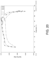
Figure 20 is a graph showing DSC scans of a composition of Sn / 0.7%Cu / 7%Bi. - The following relates generally to soldering processes and more specifically to lead-free solder containing bismuth. As described below, it has been found that a thermal treatment or processing operation can be applied to such solders to create a more reliable grain-refined solder joint with an even distribution of bismuth across the solder joint. The thermal treatment step can be incorporated into electronic assembly manufacturing, e.g., of circuit boards having soldered components.
- As is known in the art, a standard electronics assembly soldering process includes the following steps, which have been implemented in various applications for a long period of time:
- a) solder paste deposition by printing;
- b) placement of surface mount components;
- c) reflow soldering (melting of printed solder in an oven and solder joint formation)
- d) if applicable, soldering of pin through hole components by "wave" solder in a pot; and
- e) assembly cleaning as necessary.
- It has been determined that for lead-free solders containing bismuth, an additional thermal treatment step can be applied after the initial solder joint formation step, known as reflow, to improve the solder joint properties.
FIG. 1 illustrates the above process with the inclusion of this additional thermal treatment step. This thermal treatment step, which may also be referred to herein as "preconditioning", creates a more reliable grain-refined solder joint with a more even distribution of Bi across the solder joint. The thermal treatment may be combined with other assembly-level thermal treatments such as curing of conformal coating or high operating temperature burn-in. As such, the particular embodiment shown inFIG. 1 is for illustrative purposes only. The pre-conditioning step may take place before or after other processing steps which occur after reflow. The pre-conditioning step will take place before the assembly is used in the field. - In the process exemplified in
FIG. 1 , solder paste deposition is applied to the circuit board atstep 10 and surface mount components are placed on the board atstep 12. Reflow soldering is then performed atstep 14, which includes heating the board to melt the solder paste and thus form the solder joint with the leads of the component that have been aligned with the solder paste. Thethermal treatment step 16 is applied after the solder reflow step at 14 to improve the solder joints as will be described in greater detail below.Step 18 includes soldering pin through hole components, if applicable (as illustrated in dashed lines), to the board. This normally includes a wave soldering process using a pot wherein a wave of molten solder comes into contact with the through hole locations on the board as it passes over the pot to solder the through hole pins to the board. Some assembly cleaning may be necessary atstep 20, as is known in the art. This step may include a visual inspection of the soldered joints (manual or machine) as well as various other quality control measures. - It has also been found that the principles described herein can also be used for the restoration of acceptable solder joint properties after a period of time and possible use has elapsed. For example, restoration may be done after several years of product service. A similar thermal treatment step can be applied to a previously prepared solder joint containing a lead-free bismuth containing alloy. The thermal treatment step applied for "restoration" can be used to restore a more reliable grain-refined solder joint with even distribution of Bi across the solder joint, as part of a restoration and refurbishment process, after the solder interconnect structure has coarsened over time in service.
FIG. 2 illustrates an example of an application for applying theheat treatment step 16 to a previously soldered board that has been in use for a period of time. A board to be restored is obtained atstep 30 and thethermal treatment step 16 applied to one or more components on the board. A cool downstep 34 is also applied, in which new small particles precipitate evenly in the matrix, to improve thermomechanical properties as discussed in greater detail below. A preferred time for the restoration of field products may be estimated either from historical data collected for products used in the field or by estimation of the effect of diffusion rates of Bi in the solder at the field conditions. - In a particular aspect the particles of Bismuth in a bismuth containing lead-free solder joint after conditioning treatment will be smaller and more evenly distributed than the particles before conditioning.
- In a particular embodiment, the lead-free solder alloy containing bismuth further contains tin. In still a further embodiment the solder alloy includes one or more of silver and copper. In a further embodiment, the solder has a bismuth concentration between about 1 and about 10 weight percent. In a further embodiment the bismuth concentration is equal to or greater than 2 weight percent. In a particular embodiment, the bismuth concentration is between about 2 and about 7 weight percent. In another embodiment, the composition of lead-free bismuth containing solder has from 0 to 5% Ag, 0 to 1% Cu and 1 to 10% Bi with the remainder being Sn (percentages are weight percent). In a further embodiment the composition of lead-free bismuth containing solder has from >0 to 5% Ag, >0 to 1% Cu and from about 2 to 7% Bi with the remainder being Sn (percentages are weight percent).
- The term "pinning" as used herein refers to the action of a point defect which may be a second phase precipitate in a material which acts as a barrier to movement of a dislocation in the crystal structure.
- The term "intermetallic compound" or "IMC" is a solid-state compound exhibiting metallic bonding, defined stoichiometry and ordered crystal structure.
- The term "creep" or "creep rate" as used herein means the tendency of a solid material to move slowly or deform permanently under the influence of mechanical stresses, and is measured by techniques such as nano-indentation.
- The
thermal treatment step 16 is described in more detail below, making reference toFIGS. 3 through 16 . - It is generally known that solder interconnects with desirable mechanical properties can be achieved by using a material having a homogeneous structure with small grains of ductile matrix and an evenly distributed second phase pinning the grain boundaries. These features strengthen the solder material by acting as a barrier which prevents a dislocation which may occur in the material from traveling through a lattice when a relatively small stress is applied.
- It has been recognized that individual lead-free solder interconnects (solder joints) are typically composed of a few or even only one Sn-rich grain.
FIG. 3 is an SEM image which shows 3 grains in one ball grid array (BGA) interconnect. InFIG. 4 , a polarized light image of a 14x14 BGA is provided which shows single crystals with only a few crystal orientations with each joint having a different orientation. - The method of conditioning and in particular
thermal treatment step 16 described herein is aimed at converting the as-cast microstructure of the lead-free bismuth-containing alloys having large Sn dendrites (one or several grains in a solder joint) and segregated, relatively large Bi particles in the interdendritic spaces, into the desired more reliable structure having many small Sn grains and more evenly distributed Bi particles. - The overall performance of lead-free solder interconnects is dictated by the properties of β-Sn, which exhibits a significant anisotropic nature due to its special body-centered tetragonal (BCT) crystal structure with lattice parameters of a = 0.5632 nm, c = 0.3182 nm, and c/a = 0.547. Therefore, the small number of grains in an interconnect and the significant inherent anisotropic nature of the thermomechanical properties of β-Sn make Pb-free solder interconnects behave differently from their Sn-Pb counterparts, and the crystallographic orientation of each individual grain plays a very important role in dictating the overall thermomechanical performance. The stress state and strain history of every joint is different, because the orientation and boundary conditions are different.
- These anisotropic interconnects can result in at worst, unpredictable performance, and at best, electronic solder joint reliability with a wide distribution of lifetimes in the field. The specific failure mechanism that is known to occur is early life solder joint cleavage by crack propagation along a grain in response to impact or stress accumulation in the joint.
- It has also been recognized that after solidification of a lead-free bismuth-containing solder joint, the Bi particles are unevenly distributed in the microstructure as illustrated in
FIG. 5 . The Bi particles precipitate from the Sn matrix predominately between the Sn dendritic arms and in interdendritic spaces close to the intermetallic particles such as Ag3Sn and Cu6Sn5, solidifying from the last portion of liquid. The specific failure mechanism that occurs is early life solder joint cleavage by crack propagation along a grain in response to impact or stress accumulation in the joint, exacerbated by the brittleness of the precipitates. - The preconditioning and restoration treatments shown in
FIGS. 1 and2 can be used to treat electronic solder assemblies with lead-free solder comprising SnBi, Sn(Ag)Bi, Sn(Cu)Bi or Sn(Ag)CuBi to advantageously achieve better properties for the solder joints as follows. - The
thermal treatment step 16 is utilized to address the aforementioned issue with random crystal orientations and uneven microstructures. Thethermal treatment step 16 addresses this issue by obtaining a solder joint having many small randomly oriented grains with more uniformly distributed Bi particles. The resulting microstructure is somewhat similar to Sn-Pb. - The recrystallization process can significantly change the crystallographic orientation and microstructure, and therefore, the mechanical properties of the bismuth-containing, lead-free solder interconnects.
- According to the dispersion strengthening theory, the presence of second-phase particles can reinforce the solder matrix and inhibit the localized softening and deformation in the recrystallized region, improving the overall mechanical performance of lead-free solder interconnects.
- The SEM image in
FIG. 6 shows an example of the grain structure after standard reflow with a bismuth containing lead-free solder. The image shows the large Bi precipitate and uniaxial grain orientation (the corresponding grain orientation is shown inFIG. 8 using EBSD analysis).FIG. 7 shows the microstructure of the same sample after thermal treatment. The sample after the thermal treatment has small evenly distributed Bi particles in the Sn matrix with many differently oriented grains (the grain orientation is shown inFIG. 9 using EBSD analysis). -
FIG. 8 shows the grain structure after standard reflow, with large Bi precipitate (more readily visible inFIG. 6 ) and uniaxial grain orientation.FIG. 9 shows the microstructure after thermal treatment, with small evenly distributed Bi particles in Sn matrix (more easily visible inFIG. 7 ), with many differently oriented grains. The microstructures shown in the images ofFIGS. 6 through 9 are of interconnects formed using the Violet alloy having the composition Sn / 2.25%Ag / 0.5%Cu / 6%Bi, wherein the percentages are weight percentages and the Sn forms the balance of the composition.FIGS. 6 and8 are images taken after reflow and solidification, whileFIGS. 7 and9 are images taken after a conditioning treatment comprising heating the sample for 50 hours at 125°C then allowing the sample to cool, following the original reflow and solidification process. - Table 1 shows the compositions of a variety of alloys that were investigated indicating the percent weight of the components. Where the percentage of Sn is not defined in the composition, Sn is assumed to make up the balance of the composition. SnPb and SAC305 were used as standards for comparison. Different thermal treatments were performed on the alloy compositions both above the temperature of Bi dissolution in Sn (above solvus) and below the temperature of Bi dissolution in Sn (below solvus). The solvus temperature for each alloy containing Bi was experimentally determined using DSC (differential scanning calorimetry) and microstructural analysis. By way of example,
FIG. 20 shows a graph of DSC scans obtained for the Sunflower composition.FIG. 10 illustrates a solvus temperatures curve for compositions of Sn and Bi, with the Y axis showing the change in temperature in degrees celsius and the X axis showing increasing percentage of Bi from left to right; with 100% Sn at the left. The portion of the curve displayed inFIG. 10 is the tin rich portion of the phase diagram shown inFIG. 14 . The experimentally determined solvus temperatures for the compositions Senju, Violet and Sunflower (defined in Table 1) are plotted on the solvus curve shown inFIG. 10 .Table 1: Alloys Investigated Alloy number Alloy Name Composition Comment 1 SnPb Sn /37%Pb ▪ Baseline 2 SAC305 Sn / 3%Ag / 0.5%Cu ▪ Pb- free Baseline 3 Senju M42 Sn / 2%Ag / 0.75%Cu / 3%Bi ▪ Commercially Available ▪ Low Bi content 4 Violet Sn / 2.25%Ag / 0.5%Cu / 6%Bi ▪ Performed well in vibration and thermal cycling Screening Test 5 Sunflower Sn / 0.7%Cu / 7%Bi ▪ No Ag ▪ Lower cost alternative - Table 2 describes the thermal treatment parameters applied to various soldering alloys; the compositions of the alloys tested are defined in Table 1. (The "+" symbol indicates that the alloy has been tested under the condition described in the left hand columns.) The solvus line for the lead-free alloys can be found in
FIG. 10 .Table 2: Experimental Parameters for Thermal Treatments Name of thermal treatment Treatment # Parameters tested Alloys (from Table 1) Temp, °C Time, hours cycles 4 5 3 2 1 Annealing pre-conditioning 1 125 2,4,8 16, 24, 50, 100, 200 N/A + + + + 2 75 2, 4, 8 16, 24, 50, 100, 200 N/A + + + + + 3 25 24, 50, 100, 200, 1000, 2000, 6000 N/A + + + + + Cycling pre-conditioning 4 125 0.1, 0.5, 2, 8 2 + + 5 75 0.1, 0.5, 2, 8 8 + + + Annealing restoration after 70° C 300 hours6 120, 125 8, 24 N/A + + Annealing restoration after 25°C 2000 hours 7 125 8, 24 N/A + + Cycling restoration after 75° C 300hours 8 125 0.1, 0.5 2, 8 + + Cycling restoration after 25°C 2000 hours 9 125 0.1, 0.5 2, 8 + + - Data from the experiments described in Table 2 have shown that the desirable results of grain refinement and more even distribution of small Bi particles may be achieved by heating the alloys above solvus or to a temperature in the proximity of solvus. The experimental data showed that with exposure for more than 24 hours at temperatures above solvus or with exposure for 100 hours or more at temperatures below solvus good results in terms of grain refinement and more even distribution of small Bi particles is achieved.
- It has been found that by employing multiple cycles of heating and cooling, the amount of time required to achieve the desired results of grain refinement and more even Bi particle distribution can be dramatically reduced. While experimental trials using as many as 8 heating cycles were carried out, it was found that even using as few as two cycles with 10 minutes dwell at a temperature above solvus results in a structure with small grains with different orientation.
- Accordingly, a thermal treatment method has been discovered that can improve solder joints made from Pb-free alloys containing Bi. In a particular embodiment the heating temperature will be a temperature on or near the solvus line for the composition; up to 5°C below the solvus or up to 5°C above the solvus.
- In a further aspect the Pb-free bismuth containing alloy is an alloy comprising at least 2%Bi by weight. In yet another aspect the alloy has from about 0 to about 5% Ag, about 0 to about 1% Cu and about 1 to about 10% Bi with the remainder being Sn (percentages are weight percent). In a further embodiment the composition of lead-free bismuth containing solder has from >0 to about 5% Ag, >0 to about 1% Cu and from about 2 to about 7% Bi with the remainder being Sn (percentages are weight percent).
- In still a further aspect the temperature for the thermal treatment whether for annealing or cyclic treatment will be selected such that it does not exceed a temperature which would damage other aspects of the circuit board of which the solder forms a part during the selected time duration of the heating.
- In a particular aspect the
thermal treatment step 16 includes the following additional sub-steps after the reflow: - (1) Heating an electronic assembly to a temperature near the solvus of the alloy depending on the alloy used for the solder composition. For example for solder compositions as shown in
FIG. 10 and Table 3 the temperature may be in the range of 45-125 °C. - (2) Thermal exposure of the interconnect to achieve full Bi particle dissolution and even distribution of subsequently precipitated Bi particles in Sn to approach the r = 0 condition. Where in the r is the radius of the Bi particle and the radius of the Bi particle, r, is mathematically expressed as a function of the annealing time, t, by the parabolic relationship, r2= Kt. The parabolic coefficient K is a function of the temperature, T, by an Arrhenius equation of K = K0 exp(-Qk/RT), where R is the gas constant.
- (3) Cooling down to ambient temperature for recrystallization and uniform Bi particle precipitation from a solid solution of Bi in Sn.
- The compositions are defined with respect to their weight percentages with Sn making up the balance of the composition.
- Preconditioning may be done for several minutes or several hours and up to several days, in order to achieve full dissolution of the Bi particles and even distribution of the Bi across all grains in the solder joint. The time and temperature duration is dependent on the selected Bi-containing alloy. For example, Violet alloy requires up to 50 hours of thermal treatment for full Bi dissolution. Pre-conditioning (or reconditioning) under non-optimized conditions, for example, at a temperature or for a time that is not optimal may result in partial dissolution which may also provide Bi particle size and/or particle distribution which is improved over samples that have not undergone a thermal treatment step. Preconditioning or reconditioning under non-optimized conditions may still provide solder interconnects having acceptable properties depending on the application.
- In practice the time and temperature for the annealing or heat cycling step may be selected to provide suitable conditioning results and may also be adapted or conformed to other manufacturing requirements. The time for a single step annealing process may, for example, range from about 10 minutes to about 300 hours, from about 10 minutes to about 100 hours, from about 10 minutes to about 50 hours, from about 10 minutes to about 24 hours, from about 2 hours to about 50 hours or from about 2 hours to about 24 hours. The time duration for one cycle of a multicycle heating process may be from about 5 min to about 8 hours.
- Solder joint recrystallization from anisotropically oriented large grains to a grain structure of many small grains isotropically oriented (non-oriented) has been found to result in improved solder joint reliability due to improved creep and fatigue behaviour and improved global modulus.
- The interim indicator of solder joint improvement is hardness, which is known to correlate to solder joint reliability. In contrast to the SnAgCu (SAC) alloy, which loses its hardness over time at room and elevated temperature, alloys with Bi are stable and keep constant hardness under the same conditions.
- It has been found therefore that alloys of Sn(Ag)CuBi, as shown in
FIGS. 11 and12 increase or plateau in hardness with time. This illustrates the binary and ternary alloy behaviors with respect to Bi and Cu. In the bar graphs ofFIGS. 11 and12 the Y axis shows the hardness scale, Rockwell Superficial 15x, which refers to a superficial or less deep indent than standard, measured at a load of 15N where x represents the diameter of the indenter which was ¼ inch. - The reliability of these alloys in this respect has already been published. A summary of the findings on the reliability studies of SnAgCuBi alloy can be found in the reference, Journal of Microelectronics and Electronic Packaging (2015) 12, 1-29.
- Bismuth containing alloys formed excellent joints on organic solderability preservative (OSP) finish. The interfacial intermetallic layer was comparable to SnPb solders in thickness and shape, and thinner than in SAC305. The solder composition Sn2.25Ag0.5Cu6Bi (Violet), is compatible not only with OSP but also with electroless nickel immersion gold (ENIG) and electroless nickel electroless palladium immersion gold (ENEPIG), and forms excellent solder joints with uniform intermetallic layers on both BGA and leaded components.
- All combinations of alloys tested (Paul (Sn3.4Ag4.8Bi) Violet, Orchid (Sn2Ag7Bi), SAC305, and SnPb), surface finishes (OSP, ENIG, and ENEPIG), and board laminate (normal and high glass transition (Tg)) passed the aerospace ATC qualification requirement of 1,000 cycles of 55 °C to 125 °C. There was no solder joint failure on both high gloss and normal Tg boards up to 3,010 cycles for Pb-free lower melt (Paul, Violet, and Orchid) and SAC305 alloys. All three experimental alloys (i.e., Paul, Violet, and Orchid) showed excellent performance in harsh-environment thermal cycling.
- The vibration failure analysis was based on 1 million cycles at 2G and 5G, for failures found by resistance monitoring. The lowest failure rate found was for Violet at both the 2-G and 5-G levels; the failure rates were better than for SnAgCu solder alloys.
- The microstructure improvement over time at 125°C is shown in
FIG. 13 . Small equiaxial grains forming during Bi particles dissolution and Bi precipitation on grain boundaries (depicted in the schematic ofFIG. 14 ) provide exceptional creep and fatigue resistance. - Currently the electronics industry standards governing the use of soldering materials focus on the use of approved solder metal alloys, acceptable contaminant levels, and appropriate flux materials under appropriate manufacturing conditions. Specific process parameters for high reliability are not addressed. The relevant electronic industry IPC standards are listed below.
- The standards include IPC J-STD-001 Requirements for Soldered Electrical and Electronic Assemblies , J-STD-001xS Space Hardware Addendum, J-STD-004 , J-STD-005 Requirements for Soldering Pastes, J-STD-006 Requirements for Electronic Grade Solder Alloys and Fluxed and Non-Fluxed Solid Solders for Electronic Soldering Applications, IPC-A-610 Acceptability of Electronic Assemblies, IPC/WHMA-A-620 Space Hardware Addendum Space Applications Electronic Hardware Addendum for IPC/WHMA-A-620.]
- The thermal process parameters for each material are different and may be experimentally determined and verified.
- The thermal treatment process described above may be used in the electronics assembly manufacturing processes.
- With respect to the application of the
thermal treatment step 16 to restoration, it has also been recognized that lead-free solder interconnect microstructures experience coarsening over time. Sn grain size increases and Bi or other precipitants get bigger and form solid rims around grain boundaries. These properties are degrading to the function of the solder joint. - The
thermal treatment step 16 allows one to restore the microstructure and properties of lead-free alloys with solid solution and precipitation hardening. - Heating the assembly to a temperature near the solvus, allows Bi particles to be dissolved in Sn. For example, the assembly can be heated to about 65° to 100°C, for about 15 to 30 min. Following the heating step, the material is allowed to cool. During cooling, new small particles will precipitate evenly in the Sn matrix, which will improve thermomechanical properties.
- Further evidence of the improvement of mechanical properties by the conditioning treatment after aging in the field is provided by creep rate experimental data.
FIG. 19 shows the creep rate after aging for Violet alloy (defined above) compared to SAC. Aging was simulated by 300 hours baking of solder joints below solvus at 70°C. A 24 hour treatment of aged samples at 120 °C was enough to provide a significant improvement in creep resistance. In this experiment with Violet alloy, additional treatments at higher temperatures of, for example 120°C for up to 300 hours did not show a significant additional benefit. However, additional treatment at higher temperatures and longer time periods may provide some additional benefit which in may be significant in certain instances.
| Alloy | Sample |
| 1 Peak (°C) | | | Average (°C) | Difference (°C) | |
| Sunflower (Sn/0.7%Cu/7%Bi) | 83 | 82 | 82.06 | 82 | 3 |
| Sn/7%Bi | 82 | 76 | N/A | 79 | |
| Violet (Sn/2.25%Ag/0.5%Cu/6%Bi) | N/A | 86 | 92 | 89 | 7 |
| Sn/6%Bi | 82 | 82 | N/A | 82 | |
| Senju (Sn/2%Ag/0.7%Cu/3%Bi) | N/A | N/A | 42 | 42 | 6 |
| Sn/3%Bi | N/A | N/A | 36 | 36 |
Claims (6)
- A method for conditioning a solder joint in an assembly comprising:- i) obtaining an assembly having a solder joint wherein the solder joint is a lead-free solder joint comprising Bi and Sn and- ii) heating the assembly to a temperature near the solvus temperature of the alloy,wherein when the assembly has cooled the bismuth particles are smaller and more evenly distributed in the solder joint than before the heating step; andwherein the temperature near the solvus temperature of the alloy is a temperature up to 5°C below the solvus or a temperature up to 40°C above the solvus;wherein the lead-free solder joint comprises from 0 to 5 weight % Ag, 0 to 1 weight % Cu and 2 to 10 weight % Bi with the remainder being Sn; andwherein the heat treating step is performed at a temperature of from 75 °C to 130 °C; wherein the heating step is a single cycle treatment having a duration of from 10 minutes to 24 hours; or wherein the heating step is a multiple cycle treatment comprising 2 or more heating cycles, wherein each heating cycle has a duration of 5 minutes to 8 hours with a period of cooling in between.
- The method of any one of claims 1 wherein the Bi concentration is 2-7 weight %.
- The method according to any one of claims 1-2 wherein the conditioning occurs after a reflow step to form the solder joint.
- The method according to any one of claims 1-3 wherein the conditioning occurs after a period of using the assembly.
- The method according to any one of claims 1-4 wherein the temperature is 120 ± 5°C.
- A process for preparing an electronic assembly comprisinga) depositing a lead-free bismuth containing solder paste;b) placing surface mount components;c) reflow soldering; andd) conditioning the lead-free bismuth containing solder joint by the method defined in any one of claims 1-5wherein the lead-free solder joint comprises from 0 to 5 weight % Ag, 0 to 1 weight % Cu and 2 to 10 weight % Bi with the remainder being Sn.
Applications Claiming Priority (2)
| Application Number | Priority Date | Filing Date | Title |
|---|---|---|---|
| US201662294065P | 2016-02-11 | 2016-02-11 | |
| PCT/CA2017/050164 WO2017136951A1 (en) | 2016-02-11 | 2017-02-10 | Thermal treatment for preconditioning or restoration of a solder joint |
Publications (3)
| Publication Number | Publication Date |
|---|---|
| EP3414039A1 EP3414039A1 (en) | 2018-12-19 |
| EP3414039A4 EP3414039A4 (en) | 2019-11-20 |
| EP3414039B1 true EP3414039B1 (en) | 2023-06-14 |
Family
ID=59562906
Family Applications (1)
| Application Number | Title | Priority Date | Filing Date |
|---|---|---|---|
| EP17749879.7A Active EP3414039B1 (en) | 2016-02-11 | 2017-02-10 | Thermal treatment for preconditioning or restoration of a solder joint |
Country Status (6)
| Country | Link |
|---|---|
| US (2) | US20180345395A1 (en) |
| EP (1) | EP3414039B1 (en) |
| CN (1) | CN109661289A (en) |
| CA (1) | CA3014085A1 (en) |
| SG (2) | SG11201806779YA (en) |
| WO (1) | WO2017136951A1 (en) |
Families Citing this family (4)
| Publication number | Priority date | Publication date | Assignee | Title |
|---|---|---|---|---|
| CN108857132B (en) * | 2018-07-24 | 2021-04-20 | 哈尔滨工业大学(深圳) | Method for evaluating reliability of lead-free welding spot |
| US11740953B2 (en) | 2021-01-22 | 2023-08-29 | Google Llc | Solder joint damage-prevention mode for a computing device |
| JP6936926B1 (en) * | 2021-03-10 | 2021-09-22 | 千住金属工業株式会社 | Solder alloys, solder powders, solder pastes, and solder fittings |
| CN114211070B (en) * | 2021-12-31 | 2023-09-19 | 北京工业大学 | Welding method for enabling welding spot crystal grains to be oriented into multiple twin crystals |
Family Cites Families (9)
| Publication number | Priority date | Publication date | Assignee | Title |
|---|---|---|---|---|
| GB8807730D0 (en) * | 1988-03-31 | 1988-05-05 | Cookson Group Plc | Low toxicity soldering compositions |
| US5221038A (en) * | 1992-10-05 | 1993-06-22 | Motorola, Inc. | Method for forming tin-indium or tin-bismuth solder connection having increased melting temperature |
| FI98899C (en) * | 1994-10-28 | 1997-09-10 | Jorma Kalevi Kivilahti | Method for connecting electronic components by soldering |
| WO2002038326A2 (en) * | 2000-11-08 | 2002-05-16 | Corus Aluminium Walzprodukte Gmbh | Brazing product having a low melting point |
| KR100790978B1 (en) * | 2006-01-24 | 2008-01-02 | 삼성전자주식회사 | A joining method at low temperature, anda mounting method of semiconductor package using the joining method |
| KR101265449B1 (en) * | 2007-07-13 | 2013-05-16 | 센주긴조쿠고교 가부시키가이샤 | Lead-free solder for vehicle,and in-vehicle electronic circuit |
| CN102275043A (en) * | 2010-06-10 | 2011-12-14 | 中国科学院金属研究所 | Method for eliminating brittleness of connecting interface between SnBi soldering flux and Cu substrate |
| IN2014DN07833A (en) * | 2012-03-20 | 2015-04-24 | Alpha Metals | |
| US20150258636A1 (en) | 2012-10-04 | 2015-09-17 | Celestica International Inc. | Solder alloy for low-temperature processing |
-
2017
- 2017-02-10 CN CN201780011052.0A patent/CN109661289A/en active Pending
- 2017-02-10 SG SG11201806779YA patent/SG11201806779YA/en unknown
- 2017-02-10 CA CA3014085A patent/CA3014085A1/en active Pending
- 2017-02-10 EP EP17749879.7A patent/EP3414039B1/en active Active
- 2017-02-10 WO PCT/CA2017/050164 patent/WO2017136951A1/en active Application Filing
- 2017-02-10 SG SG10201914078RA patent/SG10201914078RA/en unknown
-
2018
- 2018-08-10 US US16/100,747 patent/US20180345395A1/en not_active Abandoned
-
2022
- 2022-09-26 US US17/953,315 patent/US20230249272A1/en not_active Abandoned
Also Published As
| Publication number | Publication date |
|---|---|
| EP3414039A4 (en) | 2019-11-20 |
| SG10201914078RA (en) | 2020-03-30 |
| SG11201806779YA (en) | 2018-09-27 |
| EP3414039A1 (en) | 2018-12-19 |
| CN109661289A (en) | 2019-04-19 |
| US20180345395A1 (en) | 2018-12-06 |
| US20230249272A1 (en) | 2023-08-10 |
| WO2017136951A1 (en) | 2017-08-17 |
| CA3014085A1 (en) | 2017-08-17 |
Similar Documents
| Publication | Publication Date | Title |
|---|---|---|
| US20230249272A1 (en) | Thermal Treatment for Preconditioning or Restoration of a Solder Joint | |
| Zhao et al. | Long term aging effects on the reliability of lead free solder joints in ball grid array packages with various pitch sizes and ball alignments | |
| JP4501818B2 (en) | Copper alloy material and method for producing the same | |
| EP2275224A1 (en) | Lead-free solder alloy suppressed in occurrence of shrinkage cavity | |
| JP2018518368A (en) | Reliable lead-free solder alloy for electronics applications in harsh environments | |
| KR20160006667A (en) | Semiconductor device and method for manufacturing semiconductor device | |
| Cai et al. | Mitigation of lead free solder aging effects using doped SAC-X alloys | |
| Delhaise et al. | Thermal preconditioning and restoration of bismuth-containing, lead-free solder alloys | |
| EP3707285B1 (en) | Low-silver tin based alternative solder alloy to standard sac alloys for high reliability applications | |
| KR20240013669A (en) | Solder alloy, solder ball, solder paste and solder joint | |
| Belhadi et al. | The impact of Bi content on the coarsening kinetics of IMC particles and creep deformation under thermal cycling | |
| Sujan et al. | Ball shear strength and fracture mode of lead-free solder joints prepared using nickel nanoparticle doped flux | |
| Belhadi et al. | Reliability and IMC layer evolution of homogenous lead-free solder joints during thermal cycling | |
| Tegehall | Impact of solder pad finish and solder composition on the microstructure of solder joints to various types of components | |
| JP6887183B1 (en) | Solder alloys and molded solders | |
| EP2974818B1 (en) | Solder joining method | |
| EP3707286B1 (en) | High reliability lead-free solder alloy for electronic applications in extreme environments | |
| KR20160139585A (en) | Solder alloy, solder ball and manufacturing method thereof | |
| KR102247498B1 (en) | Solder alloy, solder ball and manufacturing method thereof | |
| JP7291320B2 (en) | Method for manufacturing solder joints | |
| CN111511494B (en) | Cost-effective lead-free solder alloys for electronic applications | |
| TW202405196A (en) | Solder alloys, solder balls, solder pastes and solder joints | |
| Harcuba et al. | Microstructure and Mechanical Properties of Lead-Free Solder Joints | |
| Lau et al. | Prevailing Lead-Free Materials | |
| Lau et al. | Solder Joint Characterization |
Legal Events
| Date | Code | Title | Description |
|---|---|---|---|
| STAA | Information on the status of an ep patent application or granted ep patent |
Free format text: STATUS: THE INTERNATIONAL PUBLICATION HAS BEEN MADE |
|
| PUAI | Public reference made under article 153(3) epc to a published international application that has entered the european phase |
Free format text: ORIGINAL CODE: 0009012 |
|
| STAA | Information on the status of an ep patent application or granted ep patent |
Free format text: STATUS: REQUEST FOR EXAMINATION WAS MADE |
|
| 17P | Request for examination filed |
Effective date: 20180828 |
|
| AK | Designated contracting states |
Kind code of ref document: A1 Designated state(s): AL AT BE BG CH CY CZ DE DK EE ES FI FR GB GR HR HU IE IS IT LI LT LU LV MC MK MT NL NO PL PT RO RS SE SI SK SM TR |
|
| AX | Request for extension of the european patent |
Extension state: BA ME |
|
| STAA | Information on the status of an ep patent application or granted ep patent |
Free format text: STATUS: REQUEST FOR EXAMINATION WAS MADE |
|
| DAV | Request for validation of the european patent (deleted) | ||
| DAX | Request for extension of the european patent (deleted) | ||
| A4 | Supplementary search report drawn up and despatched |
Effective date: 20191022 |
|
| RIC1 | Information provided on ipc code assigned before grant |
Ipc: B23K 1/00 20060101AFI20191015BHEP Ipc: B23K 1/20 20060101ALI20191015BHEP |
|
| RAP1 | Party data changed (applicant data changed or rights of an application transferred) |
Owner name: CELESTICA INTERNATIONAL LP Owner name: HONEYWELL INTERNATIONAL INC. Owner name: THE GOVERNING COUNCIL OF THE UNIVERSITY OF TORONTO Owner name: ROCKWELL COLLINS, INC. Owner name: BAE SYSTEMS CONTROLS INC. Owner name: DY 4 SYSTEMS INC. |
|
| STAA | Information on the status of an ep patent application or granted ep patent |
Free format text: STATUS: EXAMINATION IS IN PROGRESS |
|
| 17Q | First examination report despatched |
Effective date: 20210303 |
|
| STAA | Information on the status of an ep patent application or granted ep patent |
Free format text: STATUS: EXAMINATION IS IN PROGRESS |
|
| GRAP | Despatch of communication of intention to grant a patent |
Free format text: ORIGINAL CODE: EPIDOSNIGR1 |
|
| STAA | Information on the status of an ep patent application or granted ep patent |
Free format text: STATUS: GRANT OF PATENT IS INTENDED |
|
| INTG | Intention to grant announced |
Effective date: 20230104 |
|
| GRAS | Grant fee paid |
Free format text: ORIGINAL CODE: EPIDOSNIGR3 |
|
| GRAA | (expected) grant |
Free format text: ORIGINAL CODE: 0009210 |
|
| STAA | Information on the status of an ep patent application or granted ep patent |
Free format text: STATUS: THE PATENT HAS BEEN GRANTED |
|
| AK | Designated contracting states |
Kind code of ref document: B1 Designated state(s): AL AT BE BG CH CY CZ DE DK EE ES FI FR GB GR HR HU IE IS IT LI LT LU LV MC MK MT NL NO PL PT RO RS SE SI SK SM TR |
|
| REG | Reference to a national code |
Ref country code: CH Ref legal event code: EP |
|
| REG | Reference to a national code |
Ref country code: DE Ref legal event code: R096 Ref document number: 602017070199 Country of ref document: DE |
|
| REG | Reference to a national code |
Ref country code: AT Ref legal event code: REF Ref document number: 1578867 Country of ref document: AT Kind code of ref document: T Effective date: 20230715 |
|
| REG | Reference to a national code |
Ref country code: LT Ref legal event code: MG9D |
|
| REG | Reference to a national code |
Ref country code: NL Ref legal event code: MP Effective date: 20230614 |
|
| PG25 | Lapsed in a contracting state [announced via postgrant information from national office to epo] |
Ref country code: SE Free format text: LAPSE BECAUSE OF FAILURE TO SUBMIT A TRANSLATION OF THE DESCRIPTION OR TO PAY THE FEE WITHIN THE PRESCRIBED TIME-LIMIT Effective date: 20230614 Ref country code: NO Free format text: LAPSE BECAUSE OF FAILURE TO SUBMIT A TRANSLATION OF THE DESCRIPTION OR TO PAY THE FEE WITHIN THE PRESCRIBED TIME-LIMIT Effective date: 20230914 Ref country code: ES Free format text: LAPSE BECAUSE OF FAILURE TO SUBMIT A TRANSLATION OF THE DESCRIPTION OR TO PAY THE FEE WITHIN THE PRESCRIBED TIME-LIMIT Effective date: 20230614 |
|
| REG | Reference to a national code |
Ref country code: AT Ref legal event code: MK05 Ref document number: 1578867 Country of ref document: AT Kind code of ref document: T Effective date: 20230614 |
|
| PG25 | Lapsed in a contracting state [announced via postgrant information from national office to epo] |
Ref country code: RS Free format text: LAPSE BECAUSE OF FAILURE TO SUBMIT A TRANSLATION OF THE DESCRIPTION OR TO PAY THE FEE WITHIN THE PRESCRIBED TIME-LIMIT Effective date: 20230614 Ref country code: NL Free format text: LAPSE BECAUSE OF FAILURE TO SUBMIT A TRANSLATION OF THE DESCRIPTION OR TO PAY THE FEE WITHIN THE PRESCRIBED TIME-LIMIT Effective date: 20230614 Ref country code: LV Free format text: LAPSE BECAUSE OF FAILURE TO SUBMIT A TRANSLATION OF THE DESCRIPTION OR TO PAY THE FEE WITHIN THE PRESCRIBED TIME-LIMIT Effective date: 20230614 Ref country code: LT Free format text: LAPSE BECAUSE OF FAILURE TO SUBMIT A TRANSLATION OF THE DESCRIPTION OR TO PAY THE FEE WITHIN THE PRESCRIBED TIME-LIMIT Effective date: 20230614 Ref country code: HR Free format text: LAPSE BECAUSE OF FAILURE TO SUBMIT A TRANSLATION OF THE DESCRIPTION OR TO PAY THE FEE WITHIN THE PRESCRIBED TIME-LIMIT Effective date: 20230614 Ref country code: GR Free format text: LAPSE BECAUSE OF FAILURE TO SUBMIT A TRANSLATION OF THE DESCRIPTION OR TO PAY THE FEE WITHIN THE PRESCRIBED TIME-LIMIT Effective date: 20230915 |
|
| PG25 | Lapsed in a contracting state [announced via postgrant information from national office to epo] |
Ref country code: FI Free format text: LAPSE BECAUSE OF FAILURE TO SUBMIT A TRANSLATION OF THE DESCRIPTION OR TO PAY THE FEE WITHIN THE PRESCRIBED TIME-LIMIT Effective date: 20230614 |
|
| PG25 | Lapsed in a contracting state [announced via postgrant information from national office to epo] |
Ref country code: SK Free format text: LAPSE BECAUSE OF FAILURE TO SUBMIT A TRANSLATION OF THE DESCRIPTION OR TO PAY THE FEE WITHIN THE PRESCRIBED TIME-LIMIT Effective date: 20230614 |
|
| PG25 | Lapsed in a contracting state [announced via postgrant information from national office to epo] |
Ref country code: IS Free format text: LAPSE BECAUSE OF FAILURE TO SUBMIT A TRANSLATION OF THE DESCRIPTION OR TO PAY THE FEE WITHIN THE PRESCRIBED TIME-LIMIT Effective date: 20231014 |
|
| PG25 | Lapsed in a contracting state [announced via postgrant information from national office to epo] |
Ref country code: SM Free format text: LAPSE BECAUSE OF FAILURE TO SUBMIT A TRANSLATION OF THE DESCRIPTION OR TO PAY THE FEE WITHIN THE PRESCRIBED TIME-LIMIT Effective date: 20230614 Ref country code: SK Free format text: LAPSE BECAUSE OF FAILURE TO SUBMIT A TRANSLATION OF THE DESCRIPTION OR TO PAY THE FEE WITHIN THE PRESCRIBED TIME-LIMIT Effective date: 20230614 Ref country code: RO Free format text: LAPSE BECAUSE OF FAILURE TO SUBMIT A TRANSLATION OF THE DESCRIPTION OR TO PAY THE FEE WITHIN THE PRESCRIBED TIME-LIMIT Effective date: 20230614 Ref country code: PT Free format text: LAPSE BECAUSE OF FAILURE TO SUBMIT A TRANSLATION OF THE DESCRIPTION OR TO PAY THE FEE WITHIN THE PRESCRIBED TIME-LIMIT Effective date: 20231016 Ref country code: IS Free format text: LAPSE BECAUSE OF FAILURE TO SUBMIT A TRANSLATION OF THE DESCRIPTION OR TO PAY THE FEE WITHIN THE PRESCRIBED TIME-LIMIT Effective date: 20231014 Ref country code: EE Free format text: LAPSE BECAUSE OF FAILURE TO SUBMIT A TRANSLATION OF THE DESCRIPTION OR TO PAY THE FEE WITHIN THE PRESCRIBED TIME-LIMIT Effective date: 20230614 Ref country code: CZ Free format text: LAPSE BECAUSE OF FAILURE TO SUBMIT A TRANSLATION OF THE DESCRIPTION OR TO PAY THE FEE WITHIN THE PRESCRIBED TIME-LIMIT Effective date: 20230614 Ref country code: AT Free format text: LAPSE BECAUSE OF FAILURE TO SUBMIT A TRANSLATION OF THE DESCRIPTION OR TO PAY THE FEE WITHIN THE PRESCRIBED TIME-LIMIT Effective date: 20230614 |
|
| PG25 | Lapsed in a contracting state [announced via postgrant information from national office to epo] |
Ref country code: PL Free format text: LAPSE BECAUSE OF FAILURE TO SUBMIT A TRANSLATION OF THE DESCRIPTION OR TO PAY THE FEE WITHIN THE PRESCRIBED TIME-LIMIT Effective date: 20230614 |
|
| PLBE | No opposition filed within time limit |
Free format text: ORIGINAL CODE: 0009261 |
|
| STAA | Information on the status of an ep patent application or granted ep patent |
Free format text: STATUS: NO OPPOSITION FILED WITHIN TIME LIMIT |