EP3410451B1 - Schirmring für eine transformatorspule - Google Patents
Schirmring für eine transformatorspule Download PDFInfo
- Publication number
- EP3410451B1 EP3410451B1 EP18170346.3A EP18170346A EP3410451B1 EP 3410451 B1 EP3410451 B1 EP 3410451B1 EP 18170346 A EP18170346 A EP 18170346A EP 3410451 B1 EP3410451 B1 EP 3410451B1
- Authority
- EP
- European Patent Office
- Prior art keywords
- grading ring
- electrically conductive
- insulating layer
- transformer according
- filler
- Prior art date
- Legal status (The legal status is an assumption and is not a legal conclusion. Google has not performed a legal analysis and makes no representation as to the accuracy of the status listed.)
- Not-in-force
Links
Images

Classifications
-
- H—ELECTRICITY
- H01—ELECTRIC ELEMENTS
- H01F—MAGNETS; INDUCTANCES; TRANSFORMERS; SELECTION OF MATERIALS FOR THEIR MAGNETIC PROPERTIES
- H01F27/00—Details of transformers or inductances, in general
- H01F27/28—Coils; Windings; Conductive connections
- H01F27/288—Shielding
- H01F27/2885—Shielding with shields or electrodes
-
- H—ELECTRICITY
- H01—ELECTRIC ELEMENTS
- H01F—MAGNETS; INDUCTANCES; TRANSFORMERS; SELECTION OF MATERIALS FOR THEIR MAGNETIC PROPERTIES
- H01F27/00—Details of transformers or inductances, in general
- H01F27/34—Special means for preventing or reducing unwanted electric or magnetic effects, e.g. no-load losses, reactive currents, harmonics, oscillations, leakage fields
- H01F27/36—Electric or magnetic shields or screens
- H01F27/363—Electric or magnetic shields or screens made of electrically conductive material
-
- H—ELECTRICITY
- H01—ELECTRIC ELEMENTS
- H01F—MAGNETS; INDUCTANCES; TRANSFORMERS; SELECTION OF MATERIALS FOR THEIR MAGNETIC PROPERTIES
- H01F27/00—Details of transformers or inductances, in general
- H01F27/34—Special means for preventing or reducing unwanted electric or magnetic effects, e.g. no-load losses, reactive currents, harmonics, oscillations, leakage fields
- H01F27/36—Electric or magnetic shields or screens
Definitions
- the invention relates to a screen ring and / or a slope compensation, as used for windings of transformers of various voltages and different power, for example for HVDC transformer coils or HVDC inductors to reduce the electrical load on the edges of the conductors.
- Windings for transformers with higher voltage and power as well as normal or low voltage and / or power are usually made from round wire, flat wire and / or twisted wire. Due to the small rounding radii of the wires, the inhomogeneity of the electrical field at the start and end of the winding and with larger distances between 2 turns - also simply called "holes" - is very high. To ensure that the windings are cooled, the insulation at these points cannot be arbitrarily designed An increase in the distances is out of the question for economic reasons. However, the electrical inhomogeneities in the electrical field can lead to flashover and thus to a defect in the transformer.
- a common approach is to reduce the inhomogeneity of the electric field. This is usually done by increasing the rounding radius. Where the radius of curvature cannot be changed or can only be changed with difficulty, the same effect can be achieved by installing one or more shield rings to control the electrical field.
- the equipotential line plots of a winding with and a winding without a shield ring it was shown that the distance between two equipotential lines, which represents the electrical load and is therefore crucial for the insulation, can be significantly increased by installing a shield ring.
- shield ring By installing a shield ring, the electrical load on the insulation is considerably reduced and the rest of the insulation structure can be designed in such a way that other boundary conditions, such as cooling of the winding, are guaranteed and the transformer can be built economically by reducing the spacing.
- known shield ring consists of a carrier material, a so-called core, which is electrically and magnetically non-conductive for this application.
- an insulating material such as block chipboard, KP wood, plastic, for example phenolic hard fabric, is used for this.
- This carrier is wrapped and / or coated with a conductive layer to control the electrical field.
- a copper fabric tape, a so-called Lahn tape, or paper coated with aluminum is used for this.
- So-called pitch compensation elements are used within the windings and at the transition to the shield ring, which, if necessary, fix the position of the winding and / or the shield ring.
- a shielding ring of more recent technology is known in which the conductive layer is not realized by a winding with a metallic fabric tape or a metallized paper, but by a conductive layer.
- the technology for producing the shield rings can of course also be used for other parts, such as pitch compensation elements in the high-voltage transformer.
- So has a shield ring next to the ring-shaped, electrically and magnetically non-conductive core, which after the DE 10 2016 205 195 according to the latest generation of shield rings and the gradient compensation elements of a transformer on an electrically conductive layer.
- This electrically conductive layer is electrically connected to the associated winding so that both have the same or a similar potential and is made as thin as possible in order to reduce eddy current losses.
- this conductive layer must not be closed in order to avoid a short circuit in the winding.
- the reason for the separation point is that, e.g. in the event of a lightning strike, an increase in voltage on the connection cable of the ring spreads in a ring to both sides and manifests itself in an electrical discharge, which in turn could damage the shield ring.
- the shield ring and slope compensation technology according to the electrically conductive layer which no longer consists of metal mesh or metal-coated paper, but at least one or more conductive layers, in particular conductive layers that can be produced by spraying, the conventional techniques using paper are used to design the separation point no longer feasible.
- the object of the present invention is therefore to overcome the disadvantages of the prior art and, in particular, to provide a technical solution, such as on a shield ring according to FIG DE 10 2016 205 195.4 the essential separation point of the first electrically conductive layer is to be generated.
- the subject matter of the present invention is a screen ring and / or pitch compensation for a transformer, comprising a core with an electrically conductive layer that surrounds the core, this electrically conductive layer being designed as a composite, which at least comprises an insulating polymer matrix with at least one fraction of electrically conductive particles, the electrically conductive filler particles being contained in an amount above the percolation threshold and containing at least one fraction of filler particles which has an average particle size in the range from 500 nm to 100 ⁇ m, the material being the filler particles is selected from the group of the following compounds: metal, carbon, metal oxide, mica, all of the aforementioned compounds as coated or uncoated particles and doped, partially doped or undoped present and / or in any mixtures of the aforementioned compounds, with a band-like, electrically conductive material is provided through which the screen ring can be handled and / or contacted to the winding and / or to ground characterized in that at the point on the shield ring which is exactly opposite the attachment
- the resistance in the electrically conductive coating at the point of separation is increased by approximately 10 times or more, in particular by 20 times or more.
- the separation point at which the electrically conductive layer overlaps to the left and right of a sub-area of the shield ring that was originally not electrically conductive coated exactly opposite the cable connection / 50 seconds - i.e. lightning strike - no short circuit is generated.
- the separation point, or the bridge formed by layer application is loaded with up to 10 kV during the test procedure.
- Figure 1 shows the longitudinal cross-section of an umbrella ring wrapped with Lahn tape and paper.
- the longitudinal cross-section can be seen in the area of the separation point, i.e. only a small sub-area of the shield ring opposite the cable connection.
- the core 1 of the shield ring which is made of pressboard, for example.
- the electrically conductive layer 2, lying on the core is implemented according to the prior art as a winding made of metallic lath tape, that is to say metallic fabric tape.
- an insulating paper 3, for example crepe paper is applied to the core.
- the separation point is thus realized in that the Lahn tape 2 is wrapped once around the screen ring, with an additional approx the underlying Lahn tape winding are electrically separated from each other by a paper winding. This means that the shield ring is a little thicker at this separation point where the lap winding overlaps.
- Figure 2 shows the same section as Figure 1 , but in the version of an electrically conductive layer of an electrically conductive lacquer, with an approx. 10 ° degree, thus for example 3 to 10 cm, in particular 5 cm wide point 4 can be seen which was not painted, where the surface of the core 1 is uncoated.
- the electrically conductive layer 5 which is covered by a lacquer according to FIG DE 10 2016 205 195.4 realized is to be recognized.
- the electrically conductive paint 5 is chosen so that its specific resistance is around 1000 ohms per square.
- an insulating material - for example a lacquer with high permittivity, as it is from the DE 10 2017 208950.4 is known, coated.
- this - advantageously sprayable material - has a resistance in ohms per square that is 10 times higher, for example 10,000 ohms per square.
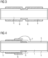
- Figure 3 is the finished separation point, starting from the first layer with "blank” according to Figure 2 could be realized.
- FIG Figure 3 the core 1 of the shield ring can also be seen again.
- FIG. 4 finally it is shown how a separation point is an alternative to the solution according to FIG Figure 3 is designed.
- the core 1 of the shield ring can be seen again.
- the electrically conductive first layer 5 lies thereon.
- the application of the electrically conductive first layer 5 begins in the area 7 of the separation point and the end of the first conductive layer 5 located in this area 7, together with part of the surface of the core 1, with an insulating second layer 6 before the all-round coating of the core 1 with the electrically conductive coating 6 is completed.
- the separation point is present in area 7, which is characterized by a triple coating, in particular a triple lacquer coating, which can preferably be applied by spraying.
- the interruption of the first, electrically conductive layer 5 is realized in such a way that at the separation point in the area 7 the two overlapping layers on the first electrically conductive layer 5 are separated from one another by an electrically insulating layer 6, in particular also for a short circuit is avoided.
- the electrically insulating layer 6 is therefore an intermediate layer in the region 7, by means of which a short circuit of the first electrically conductive layer 5 is avoided.
- the interruption of the lowermost layer 5, that is to say the one closest to the core is filled by a second, insulating layer 6, which in particular can also be applied by spraying.
- the second insulating layer 6 is preferably also a composite layer, like them
- a suitable material for the first layer of electrically conductive material 5 can, for example, from the DE 10 2016 205 195.4 , the content of which is hereby made for disclosure of the present description.
- the electrically conductive layer is designed as a composite, the at least one insulating polymer matrix with at least a fraction of electrically conductive filler particles comprises, wherein the electrically conductive filler particles are contained in an amount above the percolation threshold and contain at least one fraction of filler particles which has an average particle size in the range from 500 nm to 100 ⁇ m, the material of the filler particles being selected from the group of the following compounds: metal, carbon , Metal oxide, mica, all of the aforementioned compounds as coated or uncoated particles and doped, partially doped or undoped present and / or in any mixtures of the aforementioned compounds.
- the filler particles are in particular made of noble metal, carbon, soot, carbon tubes, in particular carbon nanotubes, graphite, fullerenes, other carbon compounds that are doped, partially doped or undoped.
- the material based on metal oxide is, for example, aluminum oxide, mica, metal oxides in binary and tertiary mixed phases, in particular tin oxide, zinc oxide, zinc stannate, titanium oxide, lead oxide, silicon carbide.
- the thickness of the electrically conductive layer is, for example, in the range less than 200 ⁇ m.
- the electrically conductive layer preferably has a square resistance of less than / equal to 10 7 ohms.
- the shape of the filler particles can be selected as desired; isotropic and / or anisotropic particles can be used.
- anisotropic particles with dimensions in the nanometer range, for example between 1 and 500 nm, are used.
- platelet-shaped particles can be used, with or without further particle shapes such as spherical particles can be used in combination.
- a suitable material for the second layer of insulating material can, for example, from the DE 10 2017208950.4 , which have a shield ring with a first electrically conductive coating of the type DE 10 2016 205 195.4 includes, on to which a second, insulating layer is applied as a type of refractive field control.
- This second insulating layer which can preferably also be applied by spraying, preferably exhibits high permittivity.
- the material for the insulating, second layer comprises at least one polyesterimide, polyamideimide, polyetherimide, epoxy, polyester, silicone, polyvinyl alcohol and / or glycerine, and any mixtures of the aforementioned classes of compounds as the base polymer.
- an electrically insulating filler with a high permittivity, but at least a permittivity higher than that of the base resin, for example higher than 3, in particular higher than 6, can be incorporated into this second insulating layer 6.
- this is a non-conductive ceramic filler such as a filler in the form of a titanate and / or spinel.
- one or more other fillers in particular mineral fillers, such as, for example, colored pigments, can be incorporated into the base resin for the electrically insulating lacquer of the second layer 6.
- the filler can be present in several fractions, these can be different in terms of material, shape and / or size of the particles.
- the insulating layer is, for example, in a layer thickness in the range from 100 ⁇ m to 500 ⁇ m, for example around 300 ⁇ m.
- the filler can be present in the second layer in a concentration of up to 30% by weight, but preferably less than 15% by weight.
- the overlap of the second electrically insulating layer 6 in the region 7 of the Figure 4 be approximately 10 cm on the left and 10 cm on the right.
- the resistance of the second, electrically insulating layer 6 is increased by 10 times compared to the first electrically conductive layer 5, but it can be increased up to 100,000 times compared to the first electrically conductive layer 5.
- the present invention discloses for the first time how the separation point, which is essential in order to avoid flashovers, can be designed in the new generation of umbrella ring.
Landscapes
- Engineering & Computer Science (AREA)
- Power Engineering (AREA)
- Regulation Of General Use Transformers (AREA)
- Laminated Bodies (AREA)
Description
- Die Erfindung betrifft einen Schirmring und/oder einen Steigungsausgleich, wie sie für Wicklungen von Transformatoren diverser Spannungen und verschiedener Leistung eingesetzt werden, beispielsweise für HGÜ-Transformatorspulen oder HGÜ-Drosselspulen zur Reduzierung der elektrischen Belastung an den Kanten der Leiter.
- Wicklungen für Transformatoren sowohl höherer Spannung und Leistung als auch normaler oder niedriger Spannung und/oder Leistung werden in der Regel aus Runddraht, Flachdraht und/oder Drilleiter hergestellt. Bedingt durch die kleinen Rundungsradien der Drähte ist die Inhomogenität des elektrischen Feldes am Wicklungsanfang, Wicklungsende und bei größeren Abständen zwischen 2 Windungen - auch einfach "Löcher genannt - sehr hoch. Um die Kühlung der Wicklungen sicherzustellen, kann die Isolation an diesen Stellen nicht beliebig gestaltet werden; eine Vergrößerung der Abstände kommt aus wirtschaftlichen Gründen nicht in Frage. Die elektrischen Inhomogenitäten im elektrischen Feld können aber zum Überschlag und somit zum Defekt des Transformators führen.
- Ein üblicher Lösungsansatz ist es, die Inhomogenität des elektrischen Feldes zu reduzieren. Dies geschieht in der Regel durch eine Vergrößerung des Rundungsradius. Dort wo sich Rundungsradien nicht oder nur schwer verändern lassen, kann die gleiche Wirkung durch den Einbau eines oder mehrerer Schirmringe zur Steuerung des elektrischen Feldes erreicht werden. In einem Vergleich der Äquipotentiallinien-Plots einer Wicklung mit und einer Wicklung ohne Schirmring konnte nachgewiesen werden, dass der Abstand zwischen zwei Äquipotentiallinien, der die elektrische Belastung darstellt und somit entscheidend für die Isolation ist, durch den Einbau eines Schirmrings entscheidend vergrößert werden kann.
- Durch den Einbau eines Schirmrings wird daher die elektrische Belastung der Isolation erheblich reduziert und der restliche Isolationsaufbau kann so gestaltet werden, dass andere Randbedingungen, wie z.B. Kühlung der Wicklung gewährleistet sind und der Transformator durch die Reduzierung von Abständen wirtschaftlich gebaut werden kann. Der gemäß der
DE 10 2011 008 462.2 bekannte Schirmring besteht aus einem Trägermaterial, einem so genannten Kern, das für diesen Anwendungsfall elektrisch und magnetisch nicht leitend ist. Eingesetzt wird dafür in der Regel ein Isolierstoff wie z.B. Blockspan, KP-Holz, Kunststoff, beispielsweise Phenolhartgewebe. Dieser Träger wird zur Steuerung des elektrischen Feldes mit einer leitfähigen Schicht umwickelt und/oder beschichtet. Herkömmlich wird dafür ein Kupfergewebeband, ein so genanntes Lahnband oder ein mit Aluminium beschichtetes Papier genutzt. - Innerhalb der Wicklungen und beim Übergang zum Schirmring kommen so genannte Steigungsausgleichselemente zum Einsatz, der gegebenenfalls die Lage der Wicklung und/oder des Schirmrings festigt.
- Aus der
DE 10 2016 205 195.4 ist ein Schirmring neuerer Technik bekannt, bei dem die leitfähige Schicht nicht durch eine Wicklung mit einem metallischen Gewebeband oder einem metallisierten Papier realisiert ist, sondern durch eine leitfähige Schicht. Die Technik zur Herstellung der Schirmringe ist selbstverständlich auch auf sonstige Teile, wie Steigungsausgleichselemente im Hochspannungstransformator anwendbar. - So weist ein Schirmring neben dem ringförmigen, elektrisch und magnetisch nicht leitfähigen Kern, der nach der
DE 10 2016 205 195 gemäß der neuesten Generation der Schirmringe und der Steigungsausgleichselemente eines Transformators eine elektrisch leitfähige Schicht auf. Diese elektrisch leitfähige Schicht wird elektrisch mit der zugehörigen Wicklung verbunden, damit beide das gleiche oder ein ähnliches Potential haben, und wird möglichst dünn ausgeführt, um Wirbelstromverluste zu reduzieren. - Diese leitfähige Schicht darf außerdem nicht geschlossen werden, um einen Kurzschluss in der Windung zu vermeiden. Der Grund für die Trennstelle liegt darin, dass z.B. bei einem Blitzschlag eine Spannungserhöhung am Anbindungskabel des Rings sich ringförmig nach beiden Seiten ausbreitet und sich in einer elektrischen Entladung äußert, die wiederum den Schirmring schädigen könnte.
- Daher wurde schon immer beim Schirmring eine so genannte Trennstelle eingebaut, an der die elektrisch leitfähige Schicht durch Isolationsmaterial unterbrochen wird.
- Wegen der Neuerungen der Schirmring und Steigungsausgleichstechnik gemäß der elektrisch leitfähigen Schicht, die nicht mehr aus Metallgewebe oder metallisch beschichtetem Papier, sondern zumindest eine oder mehrere leitfähige Schichten, insbesondere durch Besprühen herstellbare leitfähige Schichten, umfasst, sind die herkömmlichen Techniken mittels Papier zur Gestaltung der Trennstelle nicht mehr realisierbar.
- Aufgabe der vorliegenden Erfindung ist es daher, die Nachteile des Standes der Technik zu überwinden und insbesondere eine technische Lösung anzugeben, wie an ein Schirmring gemäß der
DE 10 2016 205 195.4 die essentielle Trennstelle der ersten elektrisch leitfähigen Schicht zu erzeugen ist. - Diese Aufgabe wird durch den Gegenstand der vorliegenden Anmeldung, wie er in der Beschreibung, den Figuren und den Ansprüchen offenbart ist, gelöst.
- Entsprechend ist Gegenstand der vorliegenden Erfindung ein Schirmring und/oder Steigungsausgleich für einen Transformator, einen Kern mit einer elektrisch leitfähigen, Schicht, die den Kern umschließt, umfassend, wobei diese elektrisch leitfähige Schicht als Komposit ausgeführt ist, das zumindest eine isolierende polymere Matrix mit zumindest einer Fraktion elektrisch leitfähiger Partikel umfasst, wobei die elektrisch leitfähigen Füllstoffpartikel in einer Menge oberhalb der Perkolationsschwelle enthalten sind und zumindest eine Fraktion Füllstoffpartikel enthalten, die eine mittlere Partikelgröße im Bereich von 500nm bis 100µm hat, wobei das Material der Füllstoffpartikel ausgewählt ist aus der Gruppe folgender Verbindungen: Metall, Kohlenstoff, Metalloxid, Glimmer, alle vorgenannten Verbindungen dabei als beschichtete oder unbeschichtete Partikel und dotiert, teilweise dotiert oder undotiert vorliegend und/oder in beliebigen Gemischen der vorgenannten Verbindungen, wobei an dem Schirmring ein bandartiges, elektrisch leitfähiges Material vorgesehen ist, durch das der Schirmring handhabbar und/oder an die Wicklung und/oder an Masse kontaktierbar ist
dadurch gekennzeichnet, dass
an der Stelle am Schirmring, die dem Ansatz des bandartigen elektrisch leitfähigen Materials genau gegenüberliegt, eine Trennstelle in der elektrisch leitfähigen Beschichtung vorgesehen ist, an der die elektrische Leitfähigkeit der ersten Schicht unterbrochen ist. - Nach einer vorteilhaften Ausführungsform der Erfindung ist an der Trennstelle der Widerstand in der elektrisch leitfähigen Beschichtung um das ungefähr das 10-fache oder mehr, insbesondere um das 20-fache oder mehr, erhöht.
- Beispielsweise ist die Anforderung an die Trennstelle, an der links und rechts von einem ursprünglich nicht elektrisch leitfähig beschichteten Teilbereich des Schirmrings genau gegenüber von der Kabelanbindung, die elektrisch leifähige Schicht überlappt, die, dass sie bei ca. 400 oder 500 V/mm für 1/50 Sekunde - also Blitzschlag - keinen Kurzschluss erzeugt. Insbesondere wird die Trennstelle, respektive die durch Schichtauftrag gebildete Brücke, während des Prüfverfahrens mit bis zu 10 kV belastet.
- Nach dem Stand der Technik unter Einsatz eines Metallgewebes oder eines metallisierten Papiers zur Realisierung der elektrisch leitfähigen Schicht um den Kern des Schirmrings wird die Trennstelle gemäß dem in
Figur 1 gezeigten Schemas realisiert. - In
Figur 1 ist der Längsquerschnitt eines mit Lahnband und Papier bewickelten Schirmrings gezeigt. - Zu erkennen ist der Längsquerschnitt im Bereich der Trennstelle, also nur ein kleiner Teilbereich des Schirmrings, gegenüber der Kabelanbindung. Mittig erkennt man den Kern 1 des Schirmrings, der beispielsweise aus Pressspan ist. Aufliegend auf dem Kern ist die elektrisch leitfähige Schicht 2, nach dem Stand der Technik als Wicklung aus metallischem Lahnband, sprich metallischem Gewebeband, realisiert. Im hier gezeigten Bereich der Trennstelle wird auf den Kern ein isolierendes Papier 3, beispielsweise Krepppapier, aufgebracht. Die Realisierung der Trennstelle erfolgt also dadurch dass das Lahnband 2 einmal um den Schirmring gewickelt wird, wobei nach einer Wicklung von 360° Grad noch zusätzlich ca. 20°, also beispielsweise 7 bis 15 cm, insbesondere 10 cm, weitergewickelt werden, die jedoch von der darunterliegenden Lahnbandwicklung durch eine Papierwicklung elektrisch voneinander getrennt werden. Das bedeutet, dass der Schirmring an dieser Trennstelle, an der sich die Lahnwicklung überlappt, etwas dicker ist.
- Bei der neuen Generation der Schirmringe, bei der die gewickelte Schicht durch eine gesprühte Schicht ersetzt werden soll, ist die elektrische Entkopplung der Ober- und Unterlage durch eine Papierwicklung nicht ohne weiteres umsetzbar. Deshalb wird eine Realisierung gemäß den folgenden
Figuren 2 bis 4 vorgeschlagen:
Figur 2 zeigt wieder den gleichen Ausschnitt wieFigur 1 , allerdings in der Version einer elektrisch leitfähigen Schicht eines elektrisch leitfähigen Lacks, wobei eine ca. 10 ° Grad, also beispielsweise 3 bis 10 cm, insbesondere 5 cm breite Stelle 4 zu erkennen ist, die nicht lackiert wurde, wo die Oberfläche des Kerns 1 unbeschichtet vorliegt. Rechts und links von der unbeschichteten Stelle 4 ist die elektrisch leitfähige Schicht 5, die durch einen Lack gemäß derDE 10 2016 205 195.4 realisiert ist, zu erkennen. - Beispielsweise wird der elektrisch leitfähige Lack 5 so gewählt, dass sein spezifischer Widerstand bei ca. 1000 Ohm pro Quadrat liegt. Anschließend wird mit einem isolierenden Material - beispielsweise einem Lack mit hoher Permittivität, wie er aus der
DE 10 2017 208950.4 bekannt ist, beschichtet. Beispielsweise hat dieses - vorteilhafterweise versprühbare Material - einen um das 10-fache höheren Widerstand in Ohm pro Quadrat, also beispielweise 10 000 Ohm pro Quadrat. - In
Figur 3 ist die fertige Trennstelle, ausgehend von der ersten Schicht mit "Leerstelle" gemäßFigur 2 realisiert sein könnte. Zu erkennen ist wiederum der gleiche Ausschnitt wieFigur 2 . Man sieht die isolierende zweite Schicht 6, die die Oberfläche des Kerns 1 im Bereich 4 der Trennstelle direkt bedeckt. Diese bedeckt um den Bereich 4 herum auch die elektrisch leitfähige Schicht 5. Schließlich ist inFigur 3 auch wieder der Kern 1 des Schirmrings zu erkennen. - In
Figur 4 schließlich ist gezeigt, wie eine Trennstelle alternativ zur Lösung gemäßFigur 3 konzipiert ist. Zu erkennen ist wieder der Kern 1 des Schirmrings. Auf diesem liegt die elektrisch leitfähige erste Schicht 5. Die Aufbringung der elektrisch leitfähigen ersten Schicht 5 beginnt im Bereich 7 der Trennstelle und das in diesem Bereich 7 liegende Ende der ersten leitfähigen Schicht 5 wird, zusammen mit einem Teil der Oberfläche des Kerns 1, mit einer isolierenden zweiten Schicht 6 bedeckt, bevor die Rundum-Beschichtung des Kerns 1 mit der elektrisch leitfähigen Beschichtung 6 vervollständigt ist. So ergibt sich ein Aufbau gemäß dem inFigur 1 gezeigten Stand der Technik, wobei die elektrisch leitfähige Schicht 5 und die isolierende Schicht 6 durch versprühbares Material, beispielsweise Lack, realisiert ist. Im Bereich 7 liegt in der hier gezeigten Ausführungsform die Trennstelle vor, die sich durch eine dreifache Beschichtung insbesondere eine dreifache, vorzugsweise durch Sprühen aufbringbare, LackBeschichtung, auszeichnet. - Die Unterbrechung der ersten, elektrisch leitfähigen Schicht 5 ist in der Art realisiert, dass an der Trennstelle im Bereich 7 die beiden sich überlappenden Lagen an erster elektrisch leitfähiger Schicht 5 durch eine elektrisch isolierende Schicht 6 voneinander getrennt sind, insbesondere auch deshalb, damit ein Kurzschluss vermieden wird. Die elektrisch isolierende Schicht 6 ist deshalb im Bereich 7 eine Zwischenlage, durch die ein Kurzschluss der ersten elektrisch leitfähigen Schicht 5 vermieden wird.
- Nach einer vorteilhaften Ausführungsform ist die Unterbrechung der untersten, also dem Kern am nächsten liegende, Schicht 5 durch eine zweite, isolierende Schicht 6, die insbesondere ebenfalls durch Sprühen aufbringbar ist, aufgefüllt.
- Dabei ist insbesondere bevorzugt, wenn nicht nur die Unterbrechung der leitfähigen Schicht 5, sondern links und rechts von der Unterbrechung auch noch die zweite isolierende Schicht 6 auf der ersten leitfähigen Schicht 5 aufliegt.
- Die zweite isolierende Schicht 6 ist bevorzugt ebenfalls eine Komposit-Schicht, wie sie
- Ein geeignetes Material für die erste Schicht aus elektrisch leitfähigem Material 5 kann beispielsweise aus der
DE 10 2016 205 195.4 , deren Inhalt hiermit zur Offenbarung der vorliegenden Beschreibung gemacht wird, entnommen werden. - Demnach ist die elektrisch leitfähige Schicht als Komposit ausgeführt, das zumindest eine isolierende polymere Matrix mit zumindest einer Fraktion elektrisch leitfähiger Füllstoffpartikel umfasst, wobei die elektrisch leitfähigen Füllstoffpartikel in einer Menge oberhalb der Perkolationsschwelle enthalten sind und zumindest eine Fraktion Füllstoffpartikel enthalten, die eine mittlere Partikelgröße im Bereich von 500nm bis 100µm hat, wobei das Material der Füllstoffpartikel ausgewählt ist aus der Gruppe folgender Verbindungen: Metall, Kohlenstoff, Metalloxid, Glimmer, alle vorgenannten Verbindungen dabei als beschichtete oder unbeschichtete Partikel und dotiert, teilweise dotiert oder undotiert vorliegend und/oder in beliebigen Gemischen der vorgenannten Verbindungen. Die Füllstoffpartikel sind insbesondere aus Edelmetall, Kohlenstoff, Ruß, Carbontubes, insbesondere Carbonnanotubes, Graphit, Fullerene, sonstiger Kohlenstoffverbindungen, die dotiert, teilweise dotiert oder undotiert, vorliegen.
- Das Material auf Basis von Metalloxid ist beispielsweise Aluminiumoxid, Glimmer, Metalloxide in binärer und tertiärer Mischphase, insbesondere Zinnoxid, Zinkoxid, Zinkstannat, Titanoxid, Bleioxid, Siliziumcarbid.
- Die Dicke der elektrisch leitfähigen Schicht liegt beispielsweise im Bereich kleiner 200pm. Bevorzugt hat die elektrisch leitfähige Schicht einen Quadratwiderstand von kleiner/gleich 107 Ohm.
- Die Form der Füllstoffpartikel ist dabei beliebig wählbar, es können isotrop und/oder anistrop geformte Partikel eingesetzt werden. Beispielsweise werden anisotrope Partikel, die eine Dimension im Nanometerbereich, beispielsweise zwischen 1 und 500 nm, aufweisen, eingesetzt. Wiederum beispielsweise können plättchenförmige Partikel verwendet werden, mit oder ohne weitere Partikelformen wie kugelförmige Partikel in Kombination eingesetzt werden.
- Ein geeignetes Material für die zweite Schicht aus isolierendem Material kann beispielsweise aus der
DE 10 2017208950.4 , die einen Schirmring mit einer ersten elektrisch leitfähigen Beschichtung nach Art derDE 10 2016 205 195.4 umfasst, auf den eine zweite, isolierende Schicht als eine Art refraktiver Feldsteuerung aufgebracht ist, betrifft. Diese zweite isolierende Schicht, die bevorzugt ebenfalls durch Versprühen aufbringbar ist, zeigt bevorzugt hohe Permittivität. Beispielhaft umfasst das Material für die isolierende, zweite Schicht zumindest ein Polyesterimid, Polyamidimid, Polyetherimid, Epoxid, Polyester, Silikon, Polyvinylalkohol und/oder Glycerin, sowie beliebigen Mischungen der vorgenannten Verbindungsklassen als Basispolymer. Beispielsweise kann in diese zweite isolierende Schicht 6 ein elektrisch isolierender Füllstoff mit hoher Permittivität, zumindest aber einer Permittivität höher als der des Basisharzes, also beispielsweise höher als 3, insbesondere höher als 6, eingearbeitet sein. Beispielsweise ist das ein nicht leitfähiger keramischer Füllstoff wie ein Füllstoff in Form eines Titanats und/oder Spinells. Als Beispiel dafür sei ein Farbpigment aus der Kategorie Cobald-Titan-Spinell, oder auch ein Füllstoff in Form eines Titanats mit hoher Permittivität wie Bariumtitanat, genannt. Alternativ dazu oder ergänzend können noch ein oder mehrere andere Füllstoffe, insbesondere mineralische Füllstoffe, wie beispielsweise Farbpigmente in das Basisharz für den elektrisch isolierenden Lack der zweiten Schicht 6, eingearbeitet sein. Der Füllstoff kann in mehreren Fraktionen vorliegen, diese können verschieden sein in Bezug auf Material, Form und/oder Größe der Partikel. - Diesbezüglich wird auf die
DE 10 2017208950.4 , deren Inhalt hiermit auch zum Bestandteil der vorliegenden Offenbarung gemacht wird, verwiesen. - Die isolierende Schicht liegt beispielsweise in einer Schichtdicke im Bereich von 100 µm bis 500 µm, beispielsweise um die 300 µm, vor.
- Der Füllstoff kann in der zweiten Schicht in einer Konzentration von bis zu 30 Gew% bevorzugt aber unter 15 Gew% vorliegen.
- Beispielsweise kann die Überlappung der zweiten elektrisch isolierenden Schicht 6 im Bereich 7 der
Figur 4 ungefähr 10 cm links und 10 cm rechts betragen. - Beispielsweise ist der Widerstand der zweiten, elektrisch isolierenden Schicht 6 um das 10-fache gegenüber der ersten elektrisch leitfähigen Schicht 5 erhöht, er kann aber bis zum 100.000-fachen gegenüber der ersten elektrisch leitfähigen Schicht 5 erhöht sein.
- Durch die vorliegende Erfindung wird erstmals offenbart, wie die Trennstelle, die essentiell ist, damit Überschläge vermieden werden, bei der neuen Generation an Schirmring konzipiert werden kann.
Claims (13)
- Schirmring für einen Transformator, umfassend einen Kern (1) mit einer ersten, elektrisch leitfähigen Schicht (5), die den Kern (1) umschließt, wobei die erste, elektrisch leitfähige Schicht (5) als Komposit ausgeführt ist, das zumindest eine isolierende polymere Matrix mit zumindest einer Fraktion elektrisch leitfähiger Partikel umfasst, wobei die elektrisch leitfähigen Füllstoffpartikel in einer Menge oberhalb der Perkolationsschwelle enthalten sind und zumindest eine Fraktion Füllstoffpartikel enthalten, die eine mittlere Partikelgröße im Bereich von 500nm bis 100µm hat, wobei das Material der Füllstoffpartikel ausgewählt ist aus der Gruppe folgender Verbindungen: Metall, Kohlenstoff, Metalloxid, Glimmer, alle vorgenannten Verbindungen dabei als beschichtete oder unbeschichtete Partikel und dotiert, teilweise dotiert oder undotiert vorliegend und/oder in beliebigen Gemischen der vorgenannten Verbindungen, wobei an dem Schirmring ein bandartiges, elektrisch leitfähiges Material zur Kabelanbindung an einem Ansatz befestigt ist, durch das der Schirmring handhabbar oder an Masse kontaktierbar ist und im Bereich (7) am Schirmring, der dem Ansatz des bandartigen elektrisch leitfähigen Materials zur Kabelanbindung genau gegenüberliegt, eine Trennstelle vorgesehen ist, die eine Unterbrechung der ersten elektrisch leitfähigen Schicht (5) des Schirmrings darstellt.
- Schirmring für einen Transformator nach Anspruch 1, dadurch gekennzeichnet, dass die Trennstelle im Bereich (7) durch ein Überlappen der ersten, elektrisch leitfähigen Schicht (5) mit einer Zwischenlage einer elektrisch isolierenden Schicht (6) zur Vermeidung eines Kurzschlusses erfolgt.
- Schirmring nach Anspruch 2, wobei die erste, elektrisch leitfähige Schicht (5) und/oder die zweite, elektrisch isolierende Schicht (6) aus versprühbarem Material realisiert sind.
- Schirmring für einen Transformator nach einem der vorstehenden Ansprüche, wobei die Trennstelle im Bereich (7) zwischen 3 cm bis 10 cm des Schirmrings umfasst.
- Schirmring für einen Transformator nach einem der Ansprüche 2-4, wobei die elektrisch isolierende Schicht (6) ein Lack mit einer Permittivität größer 3 ist.
- Schirmring für einen Transformator nach Anspruch 5, wobei die elektrisch isolierende Schicht (6) ein Lack mit einer Permittivität größer 6 ist.
- Schirmring für einen Transformator nach einem der vorstehenden Ansprüche 5 oder 6, wobei die zweite elektrisch isolierende Schicht (6) ein Lack auf Basis von zumindest einer Verbindung ausgewählt auf der folgenden Gruppe: Polyesterimid, Polyamidimid, Polyetherimid, Epoxid, Polyester, Silikon, Polyvinylalkohol und/oder Glycerin, sowie beliebigen Mischungen und/oder Blends der vorgenannten Verbindungen realisiert ist.
- Schirmring für einen Transformator nach einem der Ansprüche 2-7, wobei in der zweiten elektrisch isolierenden Schicht (6) ein Füllstoff eingearbeitet ist.
- Schirmring für einen Transformator nach Anspruch 8, wobei in der zweiten elektrisch isolierenden Schicht (6) Füllstoff in einer Konzentration von bis zu 30 Gew% vorliegt.
- Schirmring für einen Transformator nach einem der Ansprüche 8 oder 9, wobei in der zweiten elektrisch isolierenden Schicht (6) Füllstoff in einer Konzentration von bis zu 15 Gew% vorliegt.
- Schirmring für einen Transformator nach einem der Ansprüche 8 bis 10, wobei in der zweiten elektrisch isolierenden Schicht (6) Füllstoff, mehrere Fraktionen umfassend, vorliegt.
- Schirmring für einen Transformator nach einem der Ansprüche 2-11, wobei in der zweiten, elektrisch isolierenden Schicht (6) zumindest ein Füllstoff in Form eines Spinells vorliegt.
- Schirmring für einen Transformator nach Anspruch 12, wobei in der zweiten elektrisch isolierenden Schicht (6) zumindest ein Füllstoff in Form eines Titanats vorliegt.
Applications Claiming Priority (2)
| Application Number | Priority Date | Filing Date | Title |
|---|---|---|---|
| DE102017208980 | 2017-05-29 | ||
| DE102017212026.6A DE102017212026A1 (de) | 2017-05-29 | 2017-07-13 | Schirmring und/oder Steigungsausgleich für eine Transformatorspule |
Publications (2)
| Publication Number | Publication Date |
|---|---|
| EP3410451A1 EP3410451A1 (de) | 2018-12-05 |
| EP3410451B1 true EP3410451B1 (de) | 2021-11-17 |
Family
ID=62104186
Family Applications (1)
| Application Number | Title | Priority Date | Filing Date |
|---|---|---|---|
| EP18170346.3A Not-in-force EP3410451B1 (de) | 2017-05-29 | 2018-05-02 | Schirmring für eine transformatorspule |
Country Status (1)
| Country | Link |
|---|---|
| EP (1) | EP3410451B1 (de) |
Family Cites Families (8)
| Publication number | Priority date | Publication date | Assignee | Title |
|---|---|---|---|---|
| DE2062157A1 (de) * | 1970-12-17 | 1972-06-29 | Transformatoren Union Ag | Hochspannungsisolationsanordnung für ölgefüllte elektrische Geräte, insbesondere zur Gleichspannungsübertragung |
| CN101136281B (zh) * | 2006-08-28 | 2011-10-26 | Abb技术有限公司 | 具有屏蔽环的高压变压器、屏蔽环及屏蔽环的制造方法 |
| DE102010009462A1 (de) * | 2010-02-26 | 2011-09-01 | Siemens Aktiengesellschaft | Verfahren zum Herstellen eines Endenglimmschutzmaterials und ein Endenglimmschutz mit dem Endenglimmschutzmaterial |
| DE102011008462A1 (de) | 2011-01-07 | 2012-07-12 | Siemens Aktiengesellschaft | Schirmring für eine HGÜ-Transformatorspule oder eine HGÜ-Drosselspule |
| DE102011008454A1 (de) * | 2011-01-07 | 2012-07-26 | Siemens Aktiengesellschaft | Isolationsanordnung für eine HGÜ-Komponente mit wandartigen Feststoffbarrieren |
| DE102014211122A1 (de) * | 2014-06-11 | 2015-12-17 | Siemens Aktiengesellschaft | Elektrisch definiert leitfähiges Multifunktionsband, Verfahren zur Herstellung und Verwendung dazu |
| DE102015209594A1 (de) * | 2015-05-26 | 2016-12-01 | Siemens Aktiengesellschaft | Widerstandsbelag für einen Glimmschutz einer elektrischen Maschine |
| DE102016205195A1 (de) | 2016-02-02 | 2017-08-17 | Siemens Aktiengesellschaft | Schirmring für eine Transformatorspule |
-
2018
- 2018-05-02 EP EP18170346.3A patent/EP3410451B1/de not_active Not-in-force
Also Published As
| Publication number | Publication date |
|---|---|
| EP3410451A1 (de) | 2018-12-05 |
Similar Documents
| Publication | Publication Date | Title |
|---|---|---|
| DE3243595C2 (de) | Wicklungsanordnung für einen gasgekühlten Transformator | |
| DE69816101T2 (de) | Leistungstransformator/induktanz | |
| DE102012204052B4 (de) | Hochspannungsdurchführung mit leitenden Einlagen für Gleichspannung und Verfahren zu ihrer Herstellung | |
| DE3634946C2 (de) | Anordnung zur Übertragung eines Hochspannungsgleichstromes | |
| EP3144944A1 (de) | Elektrische wicklung, trockentransformator mit einer solchen elektrischen wicklung und verfahren zur herstellung einer elektrischen wicklung | |
| WO2009100904A1 (de) | Feldgesteuerter verbundisolator | |
| WO2017134040A1 (de) | Schirmring für eine transformatorspule | |
| CH709972A2 (de) | Elektrokabel. | |
| EP2740197B1 (de) | Elektrische leitungseinrichtung, endenglimmschutzanordnung und verfahren zum herstellen eines endenglimmschutzes | |
| EP0029164A1 (de) | Hochspannungsdurchführung | |
| CH715655B1 (de) | Durchführungshülse mit einem elektrische Leitfähigkeit selbstadaptiv regulierenden Verbundmaterial. | |
| EP4035189B1 (de) | Vorrichtung zum spannungsausgleich bei rechteckspannungen für ein elektromotor | |
| DE102017212026A1 (de) | Schirmring und/oder Steigungsausgleich für eine Transformatorspule | |
| DE102019110878B4 (de) | Kombinationskabel zur elektrischen Energie- und Datenübertragung | |
| DE19811370A1 (de) | Variation der Dielektrizitätskonstanten in Isolierungen von Hochspannungswicklungen elektrischer Maschinen | |
| EP1958217A2 (de) | Elektrische wicklung | |
| EP3410451A1 (de) | Schirmring und/oder steigungsausgleich für eine transformatorspule | |
| DE2516998A1 (de) | Einrichtung zur verhinderung von kriechentladungen | |
| DE4204092C2 (de) | Aus mindestens einer Wicklungskammer bestehender Spulenkörper für elektrisches Wickelgut, insbesondere für einen Hochspannungstransformator, sowie Hochspannungstransformator | |
| EP3410450A1 (de) | Schirmring und/oder steigungsausgleich für eine transformatorspule | |
| DE102014010777A1 (de) | Hochspannungskabel | |
| DE1465403B1 (de) | Elektrisches hochspannungskabel | |
| EP3821259A1 (de) | Spannungsteilungsvorrichtung mit siloxan-dielektrikum | |
| EP2401747B1 (de) | Elektrisches bauteil und verfahren zur herstellung eines elektrischen bauteils | |
| DE102017221593A1 (de) | Wicklungsanordnung |
Legal Events
| Date | Code | Title | Description |
|---|---|---|---|
| PUAI | Public reference made under article 153(3) epc to a published international application that has entered the european phase |
Free format text: ORIGINAL CODE: 0009012 |
|
| STAA | Information on the status of an ep patent application or granted ep patent |
Free format text: STATUS: THE APPLICATION HAS BEEN PUBLISHED |
|
| AK | Designated contracting states |
Kind code of ref document: A1 Designated state(s): AL AT BE BG CH CY CZ DE DK EE ES FI FR GB GR HR HU IE IS IT LI LT LU LV MC MK MT NL NO PL PT RO RS SE SI SK SM TR |
|
| AX | Request for extension of the european patent |
Extension state: BA ME |
|
| STAA | Information on the status of an ep patent application or granted ep patent |
Free format text: STATUS: REQUEST FOR EXAMINATION WAS MADE |
|
| 17P | Request for examination filed |
Effective date: 20190605 |
|
| RBV | Designated contracting states (corrected) |
Designated state(s): AL AT BE BG CH CY CZ DE DK EE ES FI FR GB GR HR HU IE IS IT LI LT LU LV MC MK MT NL NO PL PT RO RS SE SI SK SM TR |
|
| RAP1 | Party data changed (applicant data changed or rights of an application transferred) |
Owner name: SIEMENS ENERGY GLOBAL GMBH & CO. KG |
|
| GRAP | Despatch of communication of intention to grant a patent |
Free format text: ORIGINAL CODE: EPIDOSNIGR1 |
|
| STAA | Information on the status of an ep patent application or granted ep patent |
Free format text: STATUS: GRANT OF PATENT IS INTENDED |
|
| INTG | Intention to grant announced |
Effective date: 20210611 |
|
| GRAS | Grant fee paid |
Free format text: ORIGINAL CODE: EPIDOSNIGR3 |
|
| GRAA | (expected) grant |
Free format text: ORIGINAL CODE: 0009210 |
|
| STAA | Information on the status of an ep patent application or granted ep patent |
Free format text: STATUS: THE PATENT HAS BEEN GRANTED |
|
| AK | Designated contracting states |
Kind code of ref document: B1 Designated state(s): AL AT BE BG CH CY CZ DE DK EE ES FI FR GB GR HR HU IE IS IT LI LT LU LV MC MK MT NL NO PL PT RO RS SE SI SK SM TR |
|
| REG | Reference to a national code |
Ref country code: GB Ref legal event code: FG4D Free format text: NOT ENGLISH |
|
| REG | Reference to a national code |
Ref country code: IE Ref legal event code: FG4D Free format text: LANGUAGE OF EP DOCUMENT: GERMAN |
|
| REG | Reference to a national code |
Ref country code: DE Ref legal event code: R096 Ref document number: 502018007857 Country of ref document: DE |
|
| REG | Reference to a national code |
Ref country code: AT Ref legal event code: REF Ref document number: 1448754 Country of ref document: AT Kind code of ref document: T Effective date: 20211215 |
|
| REG | Reference to a national code |
Ref country code: LT Ref legal event code: MG9D |
|
| REG | Reference to a national code |
Ref country code: NL Ref legal event code: MP Effective date: 20211117 |
|
| PG25 | Lapsed in a contracting state [announced via postgrant information from national office to epo] |
Ref country code: RS Free format text: LAPSE BECAUSE OF FAILURE TO SUBMIT A TRANSLATION OF THE DESCRIPTION OR TO PAY THE FEE WITHIN THE PRESCRIBED TIME-LIMIT Effective date: 20211117 Ref country code: LT Free format text: LAPSE BECAUSE OF FAILURE TO SUBMIT A TRANSLATION OF THE DESCRIPTION OR TO PAY THE FEE WITHIN THE PRESCRIBED TIME-LIMIT Effective date: 20211117 Ref country code: FI Free format text: LAPSE BECAUSE OF FAILURE TO SUBMIT A TRANSLATION OF THE DESCRIPTION OR TO PAY THE FEE WITHIN THE PRESCRIBED TIME-LIMIT Effective date: 20211117 Ref country code: BG Free format text: LAPSE BECAUSE OF FAILURE TO SUBMIT A TRANSLATION OF THE DESCRIPTION OR TO PAY THE FEE WITHIN THE PRESCRIBED TIME-LIMIT Effective date: 20220217 |
|
| PG25 | Lapsed in a contracting state [announced via postgrant information from national office to epo] |
Ref country code: IS Free format text: LAPSE BECAUSE OF FAILURE TO SUBMIT A TRANSLATION OF THE DESCRIPTION OR TO PAY THE FEE WITHIN THE PRESCRIBED TIME-LIMIT Effective date: 20220317 Ref country code: SE Free format text: LAPSE BECAUSE OF FAILURE TO SUBMIT A TRANSLATION OF THE DESCRIPTION OR TO PAY THE FEE WITHIN THE PRESCRIBED TIME-LIMIT Effective date: 20211117 Ref country code: PT Free format text: LAPSE BECAUSE OF FAILURE TO SUBMIT A TRANSLATION OF THE DESCRIPTION OR TO PAY THE FEE WITHIN THE PRESCRIBED TIME-LIMIT Effective date: 20220317 Ref country code: PL Free format text: LAPSE BECAUSE OF FAILURE TO SUBMIT A TRANSLATION OF THE DESCRIPTION OR TO PAY THE FEE WITHIN THE PRESCRIBED TIME-LIMIT Effective date: 20211117 Ref country code: NO Free format text: LAPSE BECAUSE OF FAILURE TO SUBMIT A TRANSLATION OF THE DESCRIPTION OR TO PAY THE FEE WITHIN THE PRESCRIBED TIME-LIMIT Effective date: 20220217 Ref country code: NL Free format text: LAPSE BECAUSE OF FAILURE TO SUBMIT A TRANSLATION OF THE DESCRIPTION OR TO PAY THE FEE WITHIN THE PRESCRIBED TIME-LIMIT Effective date: 20211117 Ref country code: LV Free format text: LAPSE BECAUSE OF FAILURE TO SUBMIT A TRANSLATION OF THE DESCRIPTION OR TO PAY THE FEE WITHIN THE PRESCRIBED TIME-LIMIT Effective date: 20211117 Ref country code: HR Free format text: LAPSE BECAUSE OF FAILURE TO SUBMIT A TRANSLATION OF THE DESCRIPTION OR TO PAY THE FEE WITHIN THE PRESCRIBED TIME-LIMIT Effective date: 20211117 Ref country code: GR Free format text: LAPSE BECAUSE OF FAILURE TO SUBMIT A TRANSLATION OF THE DESCRIPTION OR TO PAY THE FEE WITHIN THE PRESCRIBED TIME-LIMIT Effective date: 20220218 Ref country code: ES Free format text: LAPSE BECAUSE OF FAILURE TO SUBMIT A TRANSLATION OF THE DESCRIPTION OR TO PAY THE FEE WITHIN THE PRESCRIBED TIME-LIMIT Effective date: 20211117 |
|
| PG25 | Lapsed in a contracting state [announced via postgrant information from national office to epo] |
Ref country code: SM Free format text: LAPSE BECAUSE OF FAILURE TO SUBMIT A TRANSLATION OF THE DESCRIPTION OR TO PAY THE FEE WITHIN THE PRESCRIBED TIME-LIMIT Effective date: 20211117 Ref country code: SK Free format text: LAPSE BECAUSE OF FAILURE TO SUBMIT A TRANSLATION OF THE DESCRIPTION OR TO PAY THE FEE WITHIN THE PRESCRIBED TIME-LIMIT Effective date: 20211117 Ref country code: RO Free format text: LAPSE BECAUSE OF FAILURE TO SUBMIT A TRANSLATION OF THE DESCRIPTION OR TO PAY THE FEE WITHIN THE PRESCRIBED TIME-LIMIT Effective date: 20211117 Ref country code: EE Free format text: LAPSE BECAUSE OF FAILURE TO SUBMIT A TRANSLATION OF THE DESCRIPTION OR TO PAY THE FEE WITHIN THE PRESCRIBED TIME-LIMIT Effective date: 20211117 Ref country code: DK Free format text: LAPSE BECAUSE OF FAILURE TO SUBMIT A TRANSLATION OF THE DESCRIPTION OR TO PAY THE FEE WITHIN THE PRESCRIBED TIME-LIMIT Effective date: 20211117 Ref country code: CZ Free format text: LAPSE BECAUSE OF FAILURE TO SUBMIT A TRANSLATION OF THE DESCRIPTION OR TO PAY THE FEE WITHIN THE PRESCRIBED TIME-LIMIT Effective date: 20211117 |
|
| REG | Reference to a national code |
Ref country code: DE Ref legal event code: R097 Ref document number: 502018007857 Country of ref document: DE |
|
| PLBE | No opposition filed within time limit |
Free format text: ORIGINAL CODE: 0009261 |
|
| STAA | Information on the status of an ep patent application or granted ep patent |
Free format text: STATUS: NO OPPOSITION FILED WITHIN TIME LIMIT |
|
| 26N | No opposition filed |
Effective date: 20220818 |
|
| PG25 | Lapsed in a contracting state [announced via postgrant information from national office to epo] |
Ref country code: AL Free format text: LAPSE BECAUSE OF FAILURE TO SUBMIT A TRANSLATION OF THE DESCRIPTION OR TO PAY THE FEE WITHIN THE PRESCRIBED TIME-LIMIT Effective date: 20211117 |
|
| PG25 | Lapsed in a contracting state [announced via postgrant information from national office to epo] |
Ref country code: SI Free format text: LAPSE BECAUSE OF FAILURE TO SUBMIT A TRANSLATION OF THE DESCRIPTION OR TO PAY THE FEE WITHIN THE PRESCRIBED TIME-LIMIT Effective date: 20211117 |
|
| REG | Reference to a national code |
Ref country code: DE Ref legal event code: R119 Ref document number: 502018007857 Country of ref document: DE |
|
| REG | Reference to a national code |
Ref country code: CH Ref legal event code: PL |
|
| REG | Reference to a national code |
Ref country code: BE Ref legal event code: MM Effective date: 20220531 |
|
| GBPC | Gb: european patent ceased through non-payment of renewal fee |
Effective date: 20220502 |
|
| PG25 | Lapsed in a contracting state [announced via postgrant information from national office to epo] |
Ref country code: MC Free format text: LAPSE BECAUSE OF FAILURE TO SUBMIT A TRANSLATION OF THE DESCRIPTION OR TO PAY THE FEE WITHIN THE PRESCRIBED TIME-LIMIT Effective date: 20211117 Ref country code: LU Free format text: LAPSE BECAUSE OF NON-PAYMENT OF DUE FEES Effective date: 20220502 Ref country code: LI Free format text: LAPSE BECAUSE OF NON-PAYMENT OF DUE FEES Effective date: 20220531 Ref country code: CH Free format text: LAPSE BECAUSE OF NON-PAYMENT OF DUE FEES Effective date: 20220531 |
|
| PG25 | Lapsed in a contracting state [announced via postgrant information from national office to epo] |
Ref country code: IE Free format text: LAPSE BECAUSE OF NON-PAYMENT OF DUE FEES Effective date: 20220502 Ref country code: FR Free format text: LAPSE BECAUSE OF NON-PAYMENT OF DUE FEES Effective date: 20220531 |
|
| PG25 | Lapsed in a contracting state [announced via postgrant information from national office to epo] |
Ref country code: IT Free format text: LAPSE BECAUSE OF FAILURE TO SUBMIT A TRANSLATION OF THE DESCRIPTION OR TO PAY THE FEE WITHIN THE PRESCRIBED TIME-LIMIT Effective date: 20211117 Ref country code: GB Free format text: LAPSE BECAUSE OF NON-PAYMENT OF DUE FEES Effective date: 20220502 Ref country code: DE Free format text: LAPSE BECAUSE OF NON-PAYMENT OF DUE FEES Effective date: 20221201 Ref country code: BE Free format text: LAPSE BECAUSE OF NON-PAYMENT OF DUE FEES Effective date: 20220531 |
|
| PG25 | Lapsed in a contracting state [announced via postgrant information from national office to epo] |
Ref country code: HU Free format text: LAPSE BECAUSE OF FAILURE TO SUBMIT A TRANSLATION OF THE DESCRIPTION OR TO PAY THE FEE WITHIN THE PRESCRIBED TIME-LIMIT; INVALID AB INITIO Effective date: 20180502 |
|
| PG25 | Lapsed in a contracting state [announced via postgrant information from national office to epo] |
Ref country code: MK Free format text: LAPSE BECAUSE OF FAILURE TO SUBMIT A TRANSLATION OF THE DESCRIPTION OR TO PAY THE FEE WITHIN THE PRESCRIBED TIME-LIMIT Effective date: 20211117 Ref country code: CY Free format text: LAPSE BECAUSE OF FAILURE TO SUBMIT A TRANSLATION OF THE DESCRIPTION OR TO PAY THE FEE WITHIN THE PRESCRIBED TIME-LIMIT Effective date: 20211117 |
|
| REG | Reference to a national code |
Ref country code: AT Ref legal event code: MM01 Ref document number: 1448754 Country of ref document: AT Kind code of ref document: T Effective date: 20230502 |
|
| PG25 | Lapsed in a contracting state [announced via postgrant information from national office to epo] |
Ref country code: AT Free format text: LAPSE BECAUSE OF NON-PAYMENT OF DUE FEES Effective date: 20230502 |
|
| PG25 | Lapsed in a contracting state [announced via postgrant information from national office to epo] |
Ref country code: AT Free format text: LAPSE BECAUSE OF NON-PAYMENT OF DUE FEES Effective date: 20230502 |
|
| PG25 | Lapsed in a contracting state [announced via postgrant information from national office to epo] |
Ref country code: MT Free format text: LAPSE BECAUSE OF FAILURE TO SUBMIT A TRANSLATION OF THE DESCRIPTION OR TO PAY THE FEE WITHIN THE PRESCRIBED TIME-LIMIT Effective date: 20211117 |
|
| PG25 | Lapsed in a contracting state [announced via postgrant information from national office to epo] |
Ref country code: TR Free format text: LAPSE BECAUSE OF FAILURE TO SUBMIT A TRANSLATION OF THE DESCRIPTION OR TO PAY THE FEE WITHIN THE PRESCRIBED TIME-LIMIT Effective date: 20211117 |
|
| PGFP | Annual fee paid to national office [announced via postgrant information from national office to epo] |
Ref country code: AT Payment date: 20260410 Year of fee payment: 5 |