EP3399323A1 - Elektrisches charakterisierungsverfahren eines mos-transistors auf einem soi-schaltkreis - Google Patents
Elektrisches charakterisierungsverfahren eines mos-transistors auf einem soi-schaltkreis Download PDFInfo
- Publication number
- EP3399323A1 EP3399323A1 EP18169845.7A EP18169845A EP3399323A1 EP 3399323 A1 EP3399323 A1 EP 3399323A1 EP 18169845 A EP18169845 A EP 18169845A EP 3399323 A1 EP3399323 A1 EP 3399323A1
- Authority
- EP
- European Patent Office
- Prior art keywords
- voltage
- semiconductor
- gate
- cbg
- channel
- Prior art date
- Legal status (The legal status is an assumption and is not a legal conclusion. Google has not performed a legal analysis and makes no representation as to the accuracy of the status listed.)
- Granted
Links
Images






Classifications
-
- G—PHYSICS
- G01—MEASURING; TESTING
- G01R—MEASURING ELECTRIC VARIABLES; MEASURING MAGNETIC VARIABLES
- G01R31/00—Arrangements for testing electric properties; Arrangements for locating electric faults; Arrangements for electrical testing characterised by what is being tested not provided for elsewhere
- G01R31/26—Testing of individual semiconductor devices
- G01R31/2607—Circuits therefor
- G01R31/2621—Circuits therefor for testing field effect transistors, i.e. FET's
-
- G—PHYSICS
- G01—MEASURING; TESTING
- G01R—MEASURING ELECTRIC VARIABLES; MEASURING MAGNETIC VARIABLES
- G01R31/00—Arrangements for testing electric properties; Arrangements for locating electric faults; Arrangements for electrical testing characterised by what is being tested not provided for elsewhere
- G01R31/12—Testing dielectric strength or breakdown voltage ; Testing or monitoring effectiveness or level of insulation, e.g. of a cable or of an apparatus, for example using partial discharge measurements; Electrostatic testing
- G01R31/1227—Testing dielectric strength or breakdown voltage ; Testing or monitoring effectiveness or level of insulation, e.g. of a cable or of an apparatus, for example using partial discharge measurements; Electrostatic testing of components, parts or materials
- G01R31/1263—Testing dielectric strength or breakdown voltage ; Testing or monitoring effectiveness or level of insulation, e.g. of a cable or of an apparatus, for example using partial discharge measurements; Electrostatic testing of components, parts or materials of solid or fluid materials, e.g. insulation films, bulk material; of semiconductors or LV electronic components or parts; of cable, line or wire insulation
- G01R31/129—Testing dielectric strength or breakdown voltage ; Testing or monitoring effectiveness or level of insulation, e.g. of a cable or of an apparatus, for example using partial discharge measurements; Electrostatic testing of components, parts or materials of solid or fluid materials, e.g. insulation films, bulk material; of semiconductors or LV electronic components or parts; of cable, line or wire insulation of components or parts made of semiconducting materials; of LV components or parts
-
- H—ELECTRICITY
- H10—SEMICONDUCTOR DEVICES; ELECTRIC SOLID-STATE DEVICES NOT OTHERWISE PROVIDED FOR
- H10P—GENERIC PROCESSES OR APPARATUS FOR THE MANUFACTURE OR TREATMENT OF DEVICES COVERED BY CLASS H10
- H10P74/00—Testing or measuring during manufacture or treatment of wafers, substrates or devices
- H10P74/20—Testing or measuring during manufacture or treatment of wafers, substrates or devices characterised by the properties tested or measured, e.g. structural or electrical properties
- H10P74/207—Electrical properties, e.g. testing or measuring of resistance, deep levels or capacitance-voltage characteristics
Definitions
- the present invention is in the field of electrical characterization of transistors formed by a stack of metal / oxide / semiconductor or MOS type.
- An object of the present invention is a method of measuring a set of parameters of a SOI (Silicon on Insulator) type MOS transistor.
- said set of parameters comprises the tension of flat strips at the rear face of the buried oxide.
- said set of parameters comprises the equivalent thickness of oxide EOT ("Equivalent Oxide Thickness" in English) as well as the work output of the gate metal before Weff.
- CMOS Complementary Metal Oxide Semiconductor
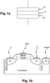
- the figure 1a shows a MOS stack formed by an M metal, an O oxide and an S semiconductor.
- figure 1b shows a transistor obtained from a MOS stack on a solid substrate on silicon.
- the figure 1b shows in particular the S source and drain D electrodes, the GAV front face gate and the PSAR rear face substrate socket.
- An alternative approach is to consider two other parameters, namely the equivalent oxide thickness EOT and the effective output work of the Weff gate metal. These two parameters are defined as being respectively the thickness of the oxide and the effective output work of the gate metal of an ideal MOS stack having the same electrical behavior as the device that is characterized.
- This MOS ideal reference stack consists of a metal, a silicon oxide dielectric having a known dielectric constant of 3.9 * 8.85 * 10 -12 F / m and a semiconductor substrate.
- the silicon oxide of this MOS stack is considered perfect, without charges and without dipoles at its interfaces.
- EOT and Weff thus define a common language for comparing two different technologies.
- a comparison from EOT and Weff makes it possible to highlight phenomena of dielectric growth or electrical shifts of reference polarizations, such as the presence of charges in dielectrics, dipoles at interfaces or work modifications. output of the gate metal.
- EOT and Weff are therefore fundamental parameters for technologists who allow them to follow suitably the process of the MOS stack and to adjust the performance of the MOS transistor. These two parameters make it possible to directly follow the thickness of the dielectric and the equivalent output work of the grid that is placed on it. This is therefore two essential leverage for a technologist to adjust the performance of the MOS transistor. They are commonly followed in process technology studies ("process technology").
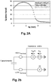
- the EOT and the Weff can be extracted from an experimental measurement of the capacity of the device that is to be characterized according to the voltage applied to the gate metal or characteristic C (V). Such a measurement can be made using the experimental setup of the figure 2b .
- a given characteristic C (V) is univocally determined from a set of three parameters formed by the EOT, the doping of the substrate and the tension of flat bands Vfb.
- This last parameter is the voltage applied to the gate respectively to the substrate and to the source and drain for which the charge in the semiconductor is zero.
- the parameter Weff is then calculated from the set of three parameters identified by the measurement of C (V), essentially the doping and the tension of flat bands.
- the figure 2a shows an example of characteristic C (V) obtained for a MOS stack deposited on a solid substrate such as that illustrated in FIGS. Figures 1a and 1b .
- the curve of the figure 2a is obtained in a known manner with the experimental setup shown in FIG. figure 2b .
- This assembly includes an impedance meter whose terminals are connected to the capacity to be determined.
- the Figures 3a and 3b illustrate the two types of capabilities that can be measured with the mounting of the figure 2b .
- This is the Cgc capacitance between GAV front panel and CH channel, illustrated in figure 3a and the Cgb capacitance between the GAV front face gate and the PSAR backplane substrate port, shown in FIG. figure 3b .
- a direct voltage Vg and an alternating voltage v (t) are applied to the front face gate GAV.
- the experimental curve illustrated in figure 2a is the capacity between grid and Cgb substrate of figure 3b . This measurement is performed for a MOS stack on a solid P-type substrate.
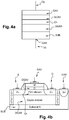
- the MOS stack on SOI illustrated at figure 4a is formed by a metal constituting the GAV front face gate, a DGAV front face gate oxide or dielectric, a Ch channel channel semiconductor layer, a second DGAR back side gate dielectric oxide or dielectric and a SUB semiconductor substrate .
- the voltage applied to the front face gate is referred to as front gate gate bias PGAV or gate voltage Vg and the voltage applied to the back face gate is referred to as back face gate bias PGAR or back face gate voltage Vb.
- the SOI MOS transistor of the figure 4b is obtained from a stack of the type illustrated in figure 4a .
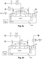
- the Figures 4c and 4d show experimental setups to measure Cgc and Cgb in the case of an SOI MOS stack.
- the characteristic C (V) relating to a MOS stack on SOI shows a variation with the reduced voltage with respect to the same measurement relating to a bulk substrate MOS stack.
- the SOI characteristic only gives access to the channel inversion part. This is for example illustrated in the figure 5a which shows a characteristic C (V) for a stack MOS, to compare with the figure 5b which shows a characteristic C (V) for a MOS stack on SOI.
- the method of adjusting the Cgc (Vg) characteristic with a theoretical model does not give very satisfactory results either.
- the figure 6 from the document Reliable Gate Stack and Substrate Parameter Extraction According to M. Mohamad et al.
- the same characteristic C (V) it is possible to obtain several sets of parameters during the adjustment between the measure and model.
- the object of the invention is to solve these problems by means of a method allowing the Weff and EOT parameters to be reliably and reproducibly extracted for a MOS stack on an SOI substrate.
- the method according to the invention also makes it possible to determine the tension of flat strips at the rear face of the buried oxide, which is not possible with the methods known to those skilled in the art.
- MOS transistor Metal / Oxide / Semiconductor on SOI substrate (Silicon on Insulator) is understood to mean a MOS transistor in which the semiconductor layer or semiconductor channel Ch of the MOS is formed on a dielectric layer. such as an oxide layer. This dielectric layer is also called DGAR back gate dielectric.
- the rear gate dielectric DGAR supporting the semiconductor channel Ch of the MOS is located above a semiconductor layer called SUB substrate of the MOS transistor on SOI. For this reason the DGAR back gate dielectric is also called buried oxide.
- FIGS. Figures 4a, 4b , 8a and 8b The structure of a SOI MOS transistor is illustrated in FIGS. Figures 4a, 4b , 8a and 8b .
- the figure 8b shows the experimental setup for the implementation of the method according to the invention.
- FIGS. Figures 1a and 1b The structure of a solid-state MOS transistor is illustrated in FIGS. Figures 1a and 1b .
- the rear face of the transistor substrate is understood to mean the external surface of the semiconductor substrate SUB.
- An electrode is applied on this external surface for the application of voltages Vbs and v (t).
- the superposition of Vbs and v (t) is also called stimulus.
- the front face grille GAV metal layer M of the MOS stack is The front face grille GAV metal layer M of the MOS stack.
- the rear panel gate GAR is understood to mean the electrode applied on the rear face of the substrate SUB of a MOS stack on SOI.
- Vfb flat-band voltage at the rear face of the DGAR buried oxide is the voltage Vbs applied to the rear face GAR of the semiconductor substrate SUB for which the charge in the semiconductor substrate SUB is zero.
- the measurement of the current Ig (t) coming from the front face GAV gate makes it possible to determine, using an impedance-meter, the capacitance Cbg, namely the capacitance between the rear face of the substrate GAR and the front face gate GAV.
- FIGS. 4c and 4d show that two different capacities can be measured with the mounting of figure 2b : the Cgb capacitance between GAV front panel and solid or bulk semiconductor, and the Cgc capacitance between GAV front panel and Ch channel.
- the impedance meter of the figure 2b makes it possible to superpose on one of its terminals a small signal voltage vg (t) that is alternative to a main voltage Vg continues. This voltage is connected to the front panel GAV of the Figures 4c and 4d .
- the second terminal of the impedance meter is connected to the source electrodes S and drain D of the MOS transistor. It is therefore possible to measure the current Ich (t) collected by source S and / or drain D and to go back to the characteristic Cgc (Vg).
- the second terminal of the impedance meter is connected to the rear face GAR of the semiconductor substrate and it is possible to go back to the characteristic Cgb (Vg).
- the capacity Cg of equation (2) is the total capacity Ctot. However, if one works in accumulation / depletion the capacity Cgb is sufficient.
- V boy Wut W F , M / q - W F , S / q + ⁇ sc + V ox q being the charge of the electron
- Equations 1, 2 and 4 therefore allow us to define in a unique way a characteristic C (V) for a stack whose characteristic parameters have been specified: the type of metal (W F, M ), the thickness of the dielectric (its thickness T ox or EOT) and the type of semiconductor (its output work W F, S and its relation between load and potential: ⁇ sc (Qsc)). If we use Vfb rather than W F, S , Vfb, EOT and ⁇ sc (Qsc) then uniquely define the characteristic C (V) from equations 1,2 and 5. However, it should be noted that these equations are complexly related to one another and that it is no longer possible to extract EOT and Vfb independently as could be the case with analytical methods.
- the figure 4a shows a MOS stack on SOI and the figure 4b shows a MOS transistor on SOI.
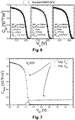
- the voltage Vfb can no longer be directly identified by the measurement. Indeed, as it is visible on Figures 5a and 5b , the characteristics C (V) measured in the two cases appear different.
- the figure 5a shows that for different gate voltages Vg the capacitance varies, which reflects a charge variation in the SUB semiconductor substrate.
- Vg negative grid voltages
- the substrate SUB is in hole reversal.
- the electrons in the substrate SUB increase until an accumulation of electrons is obtained.
- the SUB substrate necessarily goes through a zero charge condition. In other words, the rise in the capacitance for positive Vg gate voltages makes it possible to identify the condition of Vfb flat bands.
- Vfb The impossibility of accessing Vfb in the case of a MOS stack on SOI makes the usual techniques for determining the parameters Weff and EOT from the characteristic C (V) particularly complex and sometimes unreliable.
- the present invention therefore proposes a new method for the reliable determination of parameters such as Weff and EOT in the case of a MOS stack on SOI.
- the principle of the invention is based on the implementation of measurements that allow to know the load in the SUB substrate below DGAR buried oxide of the SOI structure. This makes it possible to know well the global state of polarization of the device on SOI substrate at least under the conditions of carrier inversion or depletion of the Ch channel.
- the measurement of the inversion charge of the Ch channel is well known to those skilled in the art and corresponds to the integral of the capacitance Cgc, the measurement of the charge of the substrate SUB is not common in MOS on SOI and there is no immediate way to access it.
- Cgb is zero
- the charge in the substrate SUB is not necessarily zero
- the capacitance Cgb becomes zero because it is the response of the carriers of the channel Ch, visible on the capacitance Cgc, which masks the electrostatic influence in the substrate of the fluctuations applied from the front panel GAV.
- Cgc becomes zero
- this corresponds to a cancellation of the charge of free carriers and that Cgc (Vgs) thus makes it possible to identify the channel load as a function of the Vgs polarization.
- the measure of Cgb lack of reference because the cancellation of Cgb does not mean that the SUB substrate load is canceled, but no longer varies. This characteristic therefore lacks a reference voltage for which the SUB substrate load would be zero and from which an integral of the type of equation (2) can be calculated for calculating the substrate load.
- the principle of the invention consists in identifying a suitable measurement of the charge in the substrate SUB. While the current measurement of capacitance is done by applying a stimulus on the GAV front face gate and reading the induced current on source S and drain D or on the rear face GAR, as shown in Figures 3a, 3b , 4c and 4d the method according to the invention is based on the application of the stimulus on the rear face GAR. It will therefore be possible to read the current on source S and drain D or on the front face grille GAV.
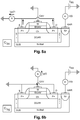
- the Figures 8a and 8b show experimental setups related to these two measurements, respectively Cbc and Cbg.
- the stimulus applied to the rear face of the transistor is constituted by the superposition of a main DC voltage Vbs and an AC voltage v (t).
- the main voltage continues Vbs can scan a predetermined range of values.
- Cbc (respectively Cbg) for the coupling between the rear face GAR and the Ch channel (respectively the coupling between the rear face GAR and the GAV front face grille).
- the second step of the method consists in determining Cbg from the current Ig (t) measured on the front face gate electrode. This step of the method thus makes it possible to obtain the characteristic Cbg (Vbs).
- the figure 9 shows that for a voltage around -6 to -4 Volts, Cbg goes out while Cgc becomes significant. As explained above, this does not mean that the charge in the GAV gate is canceled but that it no longer changes with the Vbs bias, because the Ch channel leaving the depletion regime to go into hole inversion then masks the coupling between the GAR rear panel and the GAV front panel grille. We therefore conclude that the measurement Cbg will reflect the coupling between the front panel GAV and the substrate SUB only if the channel Ch is depleted. This remark is a fundamental element in the invention. In addition to the proposed measures, the analysis must take into account this feature. From the physics point of view, this occurs when the Fermi level of the Ch channel is within the semiconductor bands.
- the variation of Vbs during the first step of the method makes it possible to measure Cbg under different load conditions, including the condition of depletion of the channel Ch.
- the condition of depletion of the channel Ch is necessary to prevent the charges in the channel. hide the response due to the capacity Cbg.
- the third step of the process consists in transforming the characteristic Cbg (Vbs) into the characteristic Cbg (Vgb).
- Vgb is the potential drop between the GAV front face gate and the GAR back face of the SUB semiconductor substrate.
- This step makes it possible to obtain a characteristic Cbg (Vgb) which directly reflects the coupling between the front face grille GAV and the rear face grille GAR. Moreover, as it is visible on the figure 11 , the characteristic Cbg (Vgb) reconstitutes a curve C (V) typical of a MOS stack on a massive substrate.
- the zone where the characteristic Cbg (Vgb) reproduces the characteristic C (V) of a solid-substrate MOS corresponds to the depletion condition of the semiconductor channel Ch.
- This significant range is therefore delimited on one side by the primer the inversion of the holes which causes an abrupt fall of Cbg to the positive Vgb voltages and on the other hand by the primer to a more negative Vgb voltage of the formation of an accumulation of electrons in the Ch channel.
- this voltage range is given as a first approximation by Eg (T box + T ch, equiv + T ox ) / (T ch, equiv + T ox ), where Eg is the gap energy of the semiconductor and T box , T ch, equiv , T ox are respectively the thicknesses of buried DGAR oxide, CH channel in equivalent thickness of silicon oxide and gate oxide or gate dielectric DGAV.
- T ch, equiv T ch . ( ⁇ SiO2 / ⁇ ch ).
- the figure 12 illustrates the adjustment step between the characteristic Cgb (Vgb) and a theoretical model for the characteristic C (V) of a solid substrate MOS stack.
- This step extracts the parameters of the equivalent MOS stack. This adjustment must necessarily be made by retaining for the characteristic C (V) the applied voltage value range Vbs for which the channel Ch is in depletion mode, so as not to mask the response of the carriers in the substrate SUB.
- the theoretical model used for the MOS stack is a simulation that takes into account the quantum properties of the stack.
- the extracted parameters may be the voltage of Vfb flat strips at the rear face of buried DGAR oxide, the output work of the front face gate electrode Weff and the equivalent oxide thickness EOT.
- the figure 13 shows a diagram of the steps of the MES measurement method of a parameter set PAR of a MOS transistor on SOI.
- the determined set of parameters comprises at least the flat band voltage Vfb at the rear face of the buried DGAR oxide.
- the set of parameters thus determined also comprises parameters such as the equivalent oxide thickness EOT and the effective output work Weff of the metal of the front face grille GAV.
- the first APP step includes applying a stimulus to the GAR backplane of the SUB substrate of the MOS transistor over SOI.
- This stimulus is formed by a main DC voltage Vbs and an AC voltage v (t).
- the main voltage Vbs can scan a range of DV voltages.
- the second MIG stage of the method comprises measuring the current Ig (t) coming from the front GAV gate before the SOI MOS transistor.
- the second step MIG also comprises measuring, from the measurement of the current Ig, the capacitance Cbg between the rear face GAR of the substrate SUB of the transistor and the front face gate GAV, so as to obtain the characteristic Cbg (Vbs).
- the first stage APP and the second stage MIG of the method MES according to the invention can be realized thanks to the assembly illustrated in FIG. figure 8b .
- the voltage Vbs and the voltage v (t) are applied to the rear face GAR of the semiconductor substrate SUB.
- the superposition of a direct voltage Vbs and of an alternating voltage v (t) makes it possible to measure the capacitance between the front-facing gate GAV and the rear face GAR of the substrate SUB of the semiconductor.
- the measurement of the capacitance can be carried out by analyzing the current Ig (t) using an impedance meter as shown in FIG. figure 2b .
- the figure 9 shows an example of characteristic Cbg (Vbs) measured thanks to the APP and MIG steps of the MES method according to the invention.
- the figure 9 also shows the characteristic Cbc (Vbs)
- the capacitance Cbc is obtained by implementing the MES method according to the invention.
- the figure 9 shows an example of characteristic Cbg (Vbs) obtained thanks to the APP and MIG steps according to the invention.
- THE figure 9 also shows a characteristic Cbc (Vbs) obtained by the same steps of the MES method according to the invention.
- the APP and MIG steps can be repeated for different voltage values Vg applied to the GAV front face gate.
- the three pairs of features shown in the figure 10 represent the characteristics Cbg and Cbc for three different values of Vg, the voltage applied to the gate electrode.
- the values of Vg are respectively -1 V, 0 V and 1V.
- the voltage Vg is not represented on the Figures 8a and 8b .
- the measurement of the characteristics Cbg and Cbc for different values of Vg makes it possible to widen the range of values of Vbs on which a variation of the values of the capacitances is observed and makes it possible to obtain a more precise extraction of the Vfb flat strip voltage. on the back side of buried DGAR oxide.
- the measurement method MES according to the invention further comprises a CARAC determination step of the characteristic Cbg (Vgb), where Vgb is the potential drop between the front-facing gate GAV and the rear face GAR of the SUB substrate.
- the characteristic Cbg (Vgb) makes it possible to account for the coupling between the front-facing gate GAV and the rear-facing gate GAR.
- each of the curves Cbg (Vgb) of the figure 11 is comparable to a part of the characteristic Cbg (Vgb) obtained for a solid-substrate MOS transistor.
- the superposition of several characteristics Cbg such as that shown in FIG. figure 11 provides a capacity measurement comparable to that of a solid-state MOS transistor over a wide range of Vgb values.
- the measurement method MES comprises a fourth step AJU for determining the parameter set PAR of the MOS transistor on SOI. This step is performed by means of an adjustment between the characteristic Cbg (Vgb) and a theoretical model describing the behavior of a solid-state MOS transistor.
- Such an adjustment is shown for example in figure 12 . This adjustment is limited to the range of Vgb values for which the Ch channel of the transistor is in depletion mode.
- the semiconductor layer behaves like a dielectric.
- the behavior of the MOS transistor on SOI is comparable to the behavior of a solid-substrate MOS transistor in which the oxide O is formed by the stack of the front-facing gate oxide DGAV, the semiconductor channel in depletion mode. Ch and buried oxide DGAR.
- the theoretical model used for the adjustment can therefore be a solid substrate MOS transistor model known to those skilled in the art.
- a simulation taking into account quantum effects can be used.
- Vfb 0.165 V
- EOT 24.8 nm
- Weff 4.47 eV.
- the EOT extracted with the MES method according to the invention is therefore an estimate of the thickness of the stack formed by the front oxide layer DGAV of thickness T ox , the semiconductor layer Ch in the depletion regime of thickness T ch, equiv and buried oxide DGAR, of thickness T box .
- the MES method according to the invention makes it possible to interpret the complex behavior of the MOS transistor on an SOI substrate by using the knowledge of the behavior of a solid-state MOS transistor.
- the MES method according to the invention further comprises a MES_Vgs step for measuring the capacitances Cgc and Cgb as a function of the voltage Vgs.
- the voltage Vgs is the voltage applied between the front face gate GAV and the source electrodes S and drain D of the semiconductor MOS on SOI substrate.
- the Cgc capacitance is the capacitance between the front panel GAV and the semiconductor channel Ch.
- the capacitance Cgb is the capacitance between the front panel GAV and the rear panel GAR of the semiconductor substrate SUB.
- the Cgc and Cgb capacitances measured in the MES_Vgs step are the capacitances measured in a manner known to those skilled in the art. These measures are represented at figure 7 . In this figure it can be seen that the Cgb capacity does not go back to the positive voltages, because the presence of buried DGAR oxide prevents the arrival of the majority carriers. It is therefore impossible to access the Vfb flat strip voltage from these measurements.
- the MES method according to the invention therefore comprises a CHARGE step for calculating the surface density of N carriers (Qtot) as a function of the voltage Vgs.
- Qtot here means the total charge which is the sum of the charges of free carriers and fixed charges:
- Q early Q ch + Q Well + Q dop , ch + Q box + Q int
- Equation (9) we find the contributions of the Ch, Q Ch channel charges, the semiconductor SUB substrate, Q Well , the depleted channel dopants, Q dop, ch , the fixed charges of the buried DGAR oxide. , Q box , and fixed charges at the interface between the DGAV front face oxide and the Ch, Q int channel.
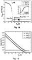
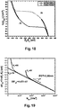
- the figure 15 shows the total carrier density N (Qtot), the surface density of carriers in the Ch N channel (Qch) and the surface density of carriers in the SUB N semiconductor substrate (QWell). These surface densities are obtained in the CHARGE step of the MES method according to the invention.
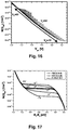
- the figure 16 shows the surface density of N carriers (Qtot) for different backplane polarizations Vb.
- the curves of the figure 16 are obtained for rear-face polarizations Vb between 6 V and -7 V.
- the curves of the figure 17 show the surface density of N (Qtot) carriers as a function of Ef-Ec.
- the different curves represent: simulations for SOI MOS transistors for different GAR backplane Vb polarizations and simulations for massive substrate MOS transistors for different semiconductor dopings.
- the surface density of the N (Qtot) carriers is related to the Ec-Ef difference through the simulations of the figure 18 and to the energy q Vgs through the curves of the figure 15 .
- the step ENE makes it possible to obtain a linear dependence between the energy E and the surface charge density Q (Ntot) or the surface density of charges Ntot.
- the Figure 19 shows this type of linear plot for the data of the Figure 7 using the relation Qtot (Vgs) shown in Figure 15 .
- the MES method according to the invention also comprises a linear adjustment step LIN of the quantity E as a function of the number of Ntot carriers.
- this step leads directly to an estimate of Weff and EOTfox which in this case are respectively 4.475 eV and 2.66nm.
- a linear adjustment also allows a simpler, more reliable and reproducible estimation of the Weff and EOTfox parameters.
- the LIN step makes it possible to deduce, with a very simple adjustment, two fundamental parameters such as the output work of the front face gate Weff and the effective thickness of the front face oxide EOTfox.
- the steps MES_Vgs, CHARGE, CARAC and AJU allow, under certain conditions of accumulation or inversion, to highlight a universal relation for a semiconductor between the field at its interface and the position of the Fermi level.
- This universal relation is coupled to the measured relationship of the total load seen at the interface with the polarization to directly extract the actual output work and the EOTfox. This extraction is made from the ordinate at the origin and the slope of the straight line thus obtained.
- the total charge seen at the interface is calculated from the SUB substrate load and the Ch channel load.
- the MES method according to the invention also makes it possible to measure the equivalent thickness T box of buried DGAR oxide, by exploiting the measured capacities Cbg and Cbc of figure 9 .
- the stack is comparable to a semiconductor / oxide / semiconductor stack.
- the MES method also comprises an additional step CHARGE_BOX for determining the charge density per unit area N (Qtot) by integrating the characteristics Cbg (Vbs) and Cbc (Vbs) of figure 9 .
- Qtot is the load seen by the concerned interface which is the rear face of the channel.
- Qtot is the sum of the Ch channel load and the GAV front face grid.
- X1 here means the affinity of the semiconductor forming the semiconductor channel, by (Ec1-Ef1) (Qtot) the characteristic resulting from the universal relation identified in Figure 18 for the channel semiconductor, by X2 the affinity of the semiconductor forming the semiconductor substrate SUB and (Ec2-Ef2) (- Qtot) the complementary characteristic to that retained for (Ec1-Ef1).
- the surface density of the N carriers (Qtot) is related to the difference Ec1-Ef1 through the universal law established in the figure 18 and at the energy q Vbs through the curves determined in step CHARGE_BOX.
- the energy Eb varies linearly as a function of the carrier density Ntot.
- X2 is identified from the ordinate at the origin of Eb and C BOX from the slope of Eb.
- the equivalent thickness of oxide T box is then determined from C BOX , in a manner known to those skilled in the art.
Landscapes
- Physics & Mathematics (AREA)
- General Physics & Mathematics (AREA)
- Engineering & Computer Science (AREA)
- Microelectronics & Electronic Packaging (AREA)
- Testing Of Individual Semiconductor Devices (AREA)
- Thin Film Transistor (AREA)
- Testing Or Measuring Of Semiconductors Or The Like (AREA)
Applications Claiming Priority (1)
| Application Number | Priority Date | Filing Date | Title |
|---|---|---|---|
| FR1753839A FR3066025B1 (fr) | 2017-05-02 | 2017-05-02 | Procede de caracterisation electrique de transistor mos sur soi |
Publications (2)
| Publication Number | Publication Date |
|---|---|
| EP3399323A1 true EP3399323A1 (de) | 2018-11-07 |
| EP3399323B1 EP3399323B1 (de) | 2022-04-27 |
Family
ID=59297063
Family Applications (1)
| Application Number | Title | Priority Date | Filing Date |
|---|---|---|---|
| EP18169845.7A Active EP3399323B1 (de) | 2017-05-02 | 2018-04-27 | Elektrisches charakterisierungsverfahren eines mos-transistors auf einem soi-schaltkreis |
Country Status (2)
| Country | Link |
|---|---|
| EP (1) | EP3399323B1 (de) |
| FR (1) | FR3066025B1 (de) |
Cited By (2)
| Publication number | Priority date | Publication date | Assignee | Title |
|---|---|---|---|---|
| CN116047257A (zh) * | 2023-03-24 | 2023-05-02 | 长鑫存储技术有限公司 | 测试方法、测试装置及电子设备 |
| CN120033099A (zh) * | 2025-04-24 | 2025-05-23 | 杭州积海半导体有限公司 | 半导体栅极结构层制作工艺的监测方法 |
Citations (4)
| Publication number | Priority date | Publication date | Assignee | Title |
|---|---|---|---|---|
| GB2351156A (en) * | 1999-06-15 | 2000-12-20 | Seiko Epson Corp | Modelling electrical characteristics of thin film transistors |
| DE102006057419A1 (de) * | 2006-01-25 | 2007-07-26 | Agilent Technologies, Inc., Palo Alto | Verfahren und Apparatur zum Messen von FET-Eigenschaften |
| EP2290386A1 (de) * | 2009-08-28 | 2011-03-02 | Commissariat à l'Énergie Atomique et aux Énergies Alternatives | Verfahren und Vorrichtung zur Auswertung der elektrischen Eigenschaften eines FDSOI Transistors |
| US8004290B1 (en) * | 2007-04-04 | 2011-08-23 | Kla-Tencor Corporation | Method and apparatus for determining dielectric layer properties |
-
2017
- 2017-05-02 FR FR1753839A patent/FR3066025B1/fr not_active Expired - Fee Related
-
2018
- 2018-04-27 EP EP18169845.7A patent/EP3399323B1/de active Active
Patent Citations (4)
| Publication number | Priority date | Publication date | Assignee | Title |
|---|---|---|---|---|
| GB2351156A (en) * | 1999-06-15 | 2000-12-20 | Seiko Epson Corp | Modelling electrical characteristics of thin film transistors |
| DE102006057419A1 (de) * | 2006-01-25 | 2007-07-26 | Agilent Technologies, Inc., Palo Alto | Verfahren und Apparatur zum Messen von FET-Eigenschaften |
| US8004290B1 (en) * | 2007-04-04 | 2011-08-23 | Kla-Tencor Corporation | Method and apparatus for determining dielectric layer properties |
| EP2290386A1 (de) * | 2009-08-28 | 2011-03-02 | Commissariat à l'Énergie Atomique et aux Énergies Alternatives | Verfahren und Vorrichtung zur Auswertung der elektrischen Eigenschaften eines FDSOI Transistors |
Non-Patent Citations (7)
| Title |
|---|
| C. LEROUX ET AL.: "Accurate détermination of flat band voltage in advanced MOS structures", MICROELECTRONICS RELIABILITY, vol. 47, 2007, pages 660 - 664 |
| HOU Y T ET AL: "Metal Gate Work Function Engineering on Gate Leakage of MOSFETs", IEEE TRANSACTIONS ON ELECTRON DEVICES, IEEE SERVICE CENTER, PISACATAWAY, NJ, US, vol. 51, no. 11, 1 November 2004 (2004-11-01), pages 1783 - 1789, XP011121194, ISSN: 0018-9383, DOI: 10.1109/TED.2004.836544 * |
| ISABELLE FERAIN ET AL: "Methodology for Flatband Voltage Measurement in Fully Depleted Floating-Body FinFETs", IEEE TRANSACTIONS ON ELECTRON DEVICES, IEEE SERVICE CENTER, PISACATAWAY, NJ, US, vol. 55, no. 7, 1 July 2008 (2008-07-01), pages 1657 - 1663, XP011216585, ISSN: 0018-9383 * |
| KWONG D-L ET AL: "Thermally Robust HfN Metal as a Promising Gate Electrode for Advanced MOS Device Applications", IEEE TRANSACTIONS ON ELECTRON DEVICES, IEEE SERVICE CENTER, PISACATAWAY, NJ, US, vol. 51, no. 4, 1 April 2004 (2004-04-01), pages 609 - 615, XP011109439, ISSN: 0018-9383, DOI: 10.1109/TED.2004.825110 * |
| LEROUX ET AL: "Accurate determination of flat band voltage in advanced MOS structure", MICROELECTRONICS AND RELIABILITY, ELSEVIER SCIENCE LTD, GB, vol. 47, no. 4-5, 21 April 2007 (2007-04-21), pages 660 - 664, XP022042384, ISSN: 0026-2714, DOI: 10.1016/J.MICROREL.2007.01.033 * |
| M. MOHAMAD, RELIABLE GATE STACK AND SUBSTRATE PARAMETER EXTRACTION BASED ON C-V MEASUREMENTS FOR 14 NM NODE FDSOI TECHNOLOGY |
| MOHAMAD B ET AL: "Reliable gate stack and substrate parameter extraction based on C-V measurements for 14nm node FDSOI technology", SOLID STATE ELECTRONICS, vol. 128, 15 October 2016 (2016-10-15), pages 10 - 16, XP029861961, ISSN: 0038-1101, DOI: 10.1016/J.SSE.2016.10.010 * |
Cited By (3)
| Publication number | Priority date | Publication date | Assignee | Title |
|---|---|---|---|---|
| CN116047257A (zh) * | 2023-03-24 | 2023-05-02 | 长鑫存储技术有限公司 | 测试方法、测试装置及电子设备 |
| CN116047257B (zh) * | 2023-03-24 | 2023-08-18 | 长鑫存储技术有限公司 | 测试方法、测试装置及电子设备 |
| CN120033099A (zh) * | 2025-04-24 | 2025-05-23 | 杭州积海半导体有限公司 | 半导体栅极结构层制作工艺的监测方法 |
Also Published As
| Publication number | Publication date |
|---|---|
| FR3066025A1 (fr) | 2018-11-09 |
| EP3399323B1 (de) | 2022-04-27 |
| FR3066025B1 (fr) | 2019-08-16 |
Similar Documents
| Publication | Publication Date | Title |
|---|---|---|
| EP2104143B1 (de) | Teststruktur eines MOS-Kondensators und Messverfahren einer Kapazitätskurve in Funktion von der entsprechenden Spannung | |
| EP2290386B1 (de) | Verfahren und Vorrichtung zur Auswertung der elektrischen Eigenschaften eines FDSOI Transistors | |
| EP2317306A1 (de) | Sensor für biologische und chemische Substanzen und Sensoranordnung | |
| EP0077862A1 (de) | Verfahren zur Bestimmung des Zuverlässigkeitsverhaltens von bipolaren Halbleiterelementen | |
| JP6441336B2 (ja) | 生物試料、化学試料又はその他の試料の電圧及び電位を測定するための装置及び方法 | |
| EP3399323B1 (de) | Elektrisches charakterisierungsverfahren eines mos-transistors auf einem soi-schaltkreis | |
| WO2006013289A1 (fr) | Capteur pour la détection et/ou la mesure d'une concentration de charges électriques contenues dans une ambiance, utilisations et procédé de fabrication correspondants. | |
| US6885214B1 (en) | Method for measuring capacitance-voltage curves for transistors | |
| WO2013175110A1 (fr) | Capteur isfet avec dispositif de controle integre | |
| EP3407076B1 (de) | Elektrisches charakterisierungsverfahren eines mos-transistors auf einem soi-schaltkreis | |
| EP3660524A1 (de) | Verfahren zur bestimmung einer korrigierten charakteristischen strom-spannungs-kurve eines elektrischen systems | |
| FR2994002A1 (fr) | Procede de determination d'un modele mathematique du comportement d'une diode a jonction pn et dispositif correspondant | |
| Nanver et al. | Test structures without metal contacts for DC measurement of 2D-materials deposited on silicon | |
| US7521946B1 (en) | Electrical measurements on semiconductors using corona and microwave techniques | |
| FR2786569A1 (fr) | Circuit de test de cellules eeprom | |
| FR3123501A1 (fr) | Capteur passif de décharges éléctrostatiques et procédé de détection de décharges électrostatiques. | |
| EP3357159A1 (de) | Elementare elektronische schaltung zur verstärkung oder wiederholung von analogen signalen | |
| FR2987134A1 (fr) | Procede et dispositif de mesure de l'evolution dans le temps des performances electriques d'un transistor fdsoi | |
| EP3889623B1 (de) | Charakterisierung von transistoren | |
| EP4060719A1 (de) | Verfahren zur bestimmung eines cet-mappings, verfahren zur bestimmung der aktivierungsenergie eines fehlertyps und entsprechende vorrichtung | |
| Gauthier | Characterization and modeling of low-frequency noise and random telegraph noise in advanced CMOS imaging technologies | |
| FR2989220A1 (fr) | Circuit integre comprenant un transistor mos ayant une reponse sigmoidale et procede de realisation correspondant | |
| JP5018053B2 (ja) | 半導体ウエーハの評価方法 | |
| JP5365174B2 (ja) | 電子デバイスの電気特性評価方法及び電子デバイスの電気特性評価装置 | |
| FR2992734A1 (fr) | Procede de caracterisation electrique d'une structure soi a quatre electrodes et dispositif associe |
Legal Events
| Date | Code | Title | Description |
|---|---|---|---|
| PUAI | Public reference made under article 153(3) epc to a published international application that has entered the european phase |
Free format text: ORIGINAL CODE: 0009012 |
|
| STAA | Information on the status of an ep patent application or granted ep patent |
Free format text: STATUS: REQUEST FOR EXAMINATION WAS MADE |
|
| 17P | Request for examination filed |
Effective date: 20180427 |
|
| AK | Designated contracting states |
Kind code of ref document: A1 Designated state(s): AL AT BE BG CH CY CZ DE DK EE ES FI FR GB GR HR HU IE IS IT LI LT LU LV MC MK MT NL NO PL PT RO RS SE SI SK SM TR |
|
| AX | Request for extension of the european patent |
Extension state: BA ME |
|
| RBV | Designated contracting states (corrected) |
Designated state(s): AL AT BE BG CH CY CZ DE DK EE ES FI FR GB GR HR HU IE IS IT LI LT LU LV MC MK MT NL NO PL PT RO RS SE SI SK SM TR |
|
| GRAP | Despatch of communication of intention to grant a patent |
Free format text: ORIGINAL CODE: EPIDOSNIGR1 |
|
| STAA | Information on the status of an ep patent application or granted ep patent |
Free format text: STATUS: GRANT OF PATENT IS INTENDED |
|
| INTG | Intention to grant announced |
Effective date: 20211119 |
|
| GRAS | Grant fee paid |
Free format text: ORIGINAL CODE: EPIDOSNIGR3 |
|
| GRAA | (expected) grant |
Free format text: ORIGINAL CODE: 0009210 |
|
| STAA | Information on the status of an ep patent application or granted ep patent |
Free format text: STATUS: THE PATENT HAS BEEN GRANTED |
|
| AK | Designated contracting states |
Kind code of ref document: B1 Designated state(s): AL AT BE BG CH CY CZ DE DK EE ES FI FR GB GR HR HU IE IS IT LI LT LU LV MC MK MT NL NO PL PT RO RS SE SI SK SM TR |
|
| REG | Reference to a national code |
Ref country code: GB Ref legal event code: FG4D Free format text: NOT ENGLISH |
|
| REG | Reference to a national code |
Ref country code: CH Ref legal event code: EP |
|
| REG | Reference to a national code |
Ref country code: AT Ref legal event code: REF Ref document number: 1487333 Country of ref document: AT Kind code of ref document: T Effective date: 20220515 |
|
| REG | Reference to a national code |
Ref country code: DE Ref legal event code: R096 Ref document number: 602018034396 Country of ref document: DE |
|
| REG | Reference to a national code |
Ref country code: IE Ref legal event code: FG4D Free format text: LANGUAGE OF EP DOCUMENT: FRENCH |
|
| REG | Reference to a national code |
Ref country code: LT Ref legal event code: MG9D |
|
| REG | Reference to a national code |
Ref country code: NL Ref legal event code: MP Effective date: 20220427 |
|
| REG | Reference to a national code |
Ref country code: AT Ref legal event code: MK05 Ref document number: 1487333 Country of ref document: AT Kind code of ref document: T Effective date: 20220427 |
|
| PG25 | Lapsed in a contracting state [announced via postgrant information from national office to epo] |
Ref country code: NL Free format text: LAPSE BECAUSE OF FAILURE TO SUBMIT A TRANSLATION OF THE DESCRIPTION OR TO PAY THE FEE WITHIN THE PRESCRIBED TIME-LIMIT Effective date: 20220427 |
|
| PG25 | Lapsed in a contracting state [announced via postgrant information from national office to epo] |
Ref country code: SE Free format text: LAPSE BECAUSE OF FAILURE TO SUBMIT A TRANSLATION OF THE DESCRIPTION OR TO PAY THE FEE WITHIN THE PRESCRIBED TIME-LIMIT Effective date: 20220427 Ref country code: PT Free format text: LAPSE BECAUSE OF FAILURE TO SUBMIT A TRANSLATION OF THE DESCRIPTION OR TO PAY THE FEE WITHIN THE PRESCRIBED TIME-LIMIT Effective date: 20220829 Ref country code: NO Free format text: LAPSE BECAUSE OF FAILURE TO SUBMIT A TRANSLATION OF THE DESCRIPTION OR TO PAY THE FEE WITHIN THE PRESCRIBED TIME-LIMIT Effective date: 20220727 Ref country code: LT Free format text: LAPSE BECAUSE OF FAILURE TO SUBMIT A TRANSLATION OF THE DESCRIPTION OR TO PAY THE FEE WITHIN THE PRESCRIBED TIME-LIMIT Effective date: 20220427 Ref country code: HR Free format text: LAPSE BECAUSE OF FAILURE TO SUBMIT A TRANSLATION OF THE DESCRIPTION OR TO PAY THE FEE WITHIN THE PRESCRIBED TIME-LIMIT Effective date: 20220427 Ref country code: GR Free format text: LAPSE BECAUSE OF FAILURE TO SUBMIT A TRANSLATION OF THE DESCRIPTION OR TO PAY THE FEE WITHIN THE PRESCRIBED TIME-LIMIT Effective date: 20220728 Ref country code: FI Free format text: LAPSE BECAUSE OF FAILURE TO SUBMIT A TRANSLATION OF THE DESCRIPTION OR TO PAY THE FEE WITHIN THE PRESCRIBED TIME-LIMIT Effective date: 20220427 Ref country code: ES Free format text: LAPSE BECAUSE OF FAILURE TO SUBMIT A TRANSLATION OF THE DESCRIPTION OR TO PAY THE FEE WITHIN THE PRESCRIBED TIME-LIMIT Effective date: 20220427 Ref country code: BG Free format text: LAPSE BECAUSE OF FAILURE TO SUBMIT A TRANSLATION OF THE DESCRIPTION OR TO PAY THE FEE WITHIN THE PRESCRIBED TIME-LIMIT Effective date: 20220727 Ref country code: AT Free format text: LAPSE BECAUSE OF FAILURE TO SUBMIT A TRANSLATION OF THE DESCRIPTION OR TO PAY THE FEE WITHIN THE PRESCRIBED TIME-LIMIT Effective date: 20220427 |
|
| PG25 | Lapsed in a contracting state [announced via postgrant information from national office to epo] |
Ref country code: RS Free format text: LAPSE BECAUSE OF FAILURE TO SUBMIT A TRANSLATION OF THE DESCRIPTION OR TO PAY THE FEE WITHIN THE PRESCRIBED TIME-LIMIT Effective date: 20220427 Ref country code: PL Free format text: LAPSE BECAUSE OF FAILURE TO SUBMIT A TRANSLATION OF THE DESCRIPTION OR TO PAY THE FEE WITHIN THE PRESCRIBED TIME-LIMIT Effective date: 20220427 Ref country code: LV Free format text: LAPSE BECAUSE OF FAILURE TO SUBMIT A TRANSLATION OF THE DESCRIPTION OR TO PAY THE FEE WITHIN THE PRESCRIBED TIME-LIMIT Effective date: 20220427 Ref country code: IS Free format text: LAPSE BECAUSE OF FAILURE TO SUBMIT A TRANSLATION OF THE DESCRIPTION OR TO PAY THE FEE WITHIN THE PRESCRIBED TIME-LIMIT Effective date: 20220827 |
|
| REG | Reference to a national code |
Ref country code: CH Ref legal event code: PL |
|
| REG | Reference to a national code |
Ref country code: DE Ref legal event code: R097 Ref document number: 602018034396 Country of ref document: DE |
|
| PG25 | Lapsed in a contracting state [announced via postgrant information from national office to epo] |
Ref country code: SM Free format text: LAPSE BECAUSE OF FAILURE TO SUBMIT A TRANSLATION OF THE DESCRIPTION OR TO PAY THE FEE WITHIN THE PRESCRIBED TIME-LIMIT Effective date: 20220427 Ref country code: SK Free format text: LAPSE BECAUSE OF FAILURE TO SUBMIT A TRANSLATION OF THE DESCRIPTION OR TO PAY THE FEE WITHIN THE PRESCRIBED TIME-LIMIT Effective date: 20220427 Ref country code: RO Free format text: LAPSE BECAUSE OF FAILURE TO SUBMIT A TRANSLATION OF THE DESCRIPTION OR TO PAY THE FEE WITHIN THE PRESCRIBED TIME-LIMIT Effective date: 20220427 Ref country code: MC Free format text: LAPSE BECAUSE OF FAILURE TO SUBMIT A TRANSLATION OF THE DESCRIPTION OR TO PAY THE FEE WITHIN THE PRESCRIBED TIME-LIMIT Effective date: 20220427 Ref country code: LU Free format text: LAPSE BECAUSE OF NON-PAYMENT OF DUE FEES Effective date: 20220427 Ref country code: LI Free format text: LAPSE BECAUSE OF NON-PAYMENT OF DUE FEES Effective date: 20220430 Ref country code: EE Free format text: LAPSE BECAUSE OF FAILURE TO SUBMIT A TRANSLATION OF THE DESCRIPTION OR TO PAY THE FEE WITHIN THE PRESCRIBED TIME-LIMIT Effective date: 20220427 Ref country code: DK Free format text: LAPSE BECAUSE OF FAILURE TO SUBMIT A TRANSLATION OF THE DESCRIPTION OR TO PAY THE FEE WITHIN THE PRESCRIBED TIME-LIMIT Effective date: 20220427 Ref country code: CZ Free format text: LAPSE BECAUSE OF FAILURE TO SUBMIT A TRANSLATION OF THE DESCRIPTION OR TO PAY THE FEE WITHIN THE PRESCRIBED TIME-LIMIT Effective date: 20220427 Ref country code: CH Free format text: LAPSE BECAUSE OF NON-PAYMENT OF DUE FEES Effective date: 20220430 |
|
| PLBE | No opposition filed within time limit |
Free format text: ORIGINAL CODE: 0009261 |
|
| STAA | Information on the status of an ep patent application or granted ep patent |
Free format text: STATUS: NO OPPOSITION FILED WITHIN TIME LIMIT |
|
| PG25 | Lapsed in a contracting state [announced via postgrant information from national office to epo] |
Ref country code: AL Free format text: LAPSE BECAUSE OF FAILURE TO SUBMIT A TRANSLATION OF THE DESCRIPTION OR TO PAY THE FEE WITHIN THE PRESCRIBED TIME-LIMIT Effective date: 20220427 |
|
| 26N | No opposition filed |
Effective date: 20230130 |
|
| PG25 | Lapsed in a contracting state [announced via postgrant information from national office to epo] |
Ref country code: IE Free format text: LAPSE BECAUSE OF NON-PAYMENT OF DUE FEES Effective date: 20220427 |
|
| PG25 | Lapsed in a contracting state [announced via postgrant information from national office to epo] |
Ref country code: SI Free format text: LAPSE BECAUSE OF FAILURE TO SUBMIT A TRANSLATION OF THE DESCRIPTION OR TO PAY THE FEE WITHIN THE PRESCRIBED TIME-LIMIT Effective date: 20220427 |
|
| PG25 | Lapsed in a contracting state [announced via postgrant information from national office to epo] |
Ref country code: IT Free format text: LAPSE BECAUSE OF FAILURE TO SUBMIT A TRANSLATION OF THE DESCRIPTION OR TO PAY THE FEE WITHIN THE PRESCRIBED TIME-LIMIT Effective date: 20220427 |
|
| PG25 | Lapsed in a contracting state [announced via postgrant information from national office to epo] |
Ref country code: HU Free format text: LAPSE BECAUSE OF FAILURE TO SUBMIT A TRANSLATION OF THE DESCRIPTION OR TO PAY THE FEE WITHIN THE PRESCRIBED TIME-LIMIT; INVALID AB INITIO Effective date: 20180427 |
|
| PG25 | Lapsed in a contracting state [announced via postgrant information from national office to epo] |
Ref country code: MK Free format text: LAPSE BECAUSE OF FAILURE TO SUBMIT A TRANSLATION OF THE DESCRIPTION OR TO PAY THE FEE WITHIN THE PRESCRIBED TIME-LIMIT Effective date: 20220427 Ref country code: CY Free format text: LAPSE BECAUSE OF FAILURE TO SUBMIT A TRANSLATION OF THE DESCRIPTION OR TO PAY THE FEE WITHIN THE PRESCRIBED TIME-LIMIT Effective date: 20220427 |
|
| PG25 | Lapsed in a contracting state [announced via postgrant information from national office to epo] |
Ref country code: MT Free format text: LAPSE BECAUSE OF FAILURE TO SUBMIT A TRANSLATION OF THE DESCRIPTION OR TO PAY THE FEE WITHIN THE PRESCRIBED TIME-LIMIT Effective date: 20220427 |
|
| PG25 | Lapsed in a contracting state [announced via postgrant information from national office to epo] |
Ref country code: BG Free format text: LAPSE BECAUSE OF FAILURE TO SUBMIT A TRANSLATION OF THE DESCRIPTION OR TO PAY THE FEE WITHIN THE PRESCRIBED TIME-LIMIT Effective date: 20220427 |
|
| PG25 | Lapsed in a contracting state [announced via postgrant information from national office to epo] |
Ref country code: BG Free format text: LAPSE BECAUSE OF FAILURE TO SUBMIT A TRANSLATION OF THE DESCRIPTION OR TO PAY THE FEE WITHIN THE PRESCRIBED TIME-LIMIT Effective date: 20220427 |
|
| PGFP | Annual fee paid to national office [announced via postgrant information from national office to epo] |
Ref country code: DE Payment date: 20250417 Year of fee payment: 8 |
|
| PGFP | Annual fee paid to national office [announced via postgrant information from national office to epo] |
Ref country code: GB Payment date: 20250424 Year of fee payment: 8 |
|
| PGFP | Annual fee paid to national office [announced via postgrant information from national office to epo] |
Ref country code: BE Payment date: 20250417 Year of fee payment: 8 |
|
| PGFP | Annual fee paid to national office [announced via postgrant information from national office to epo] |
Ref country code: FR Payment date: 20250422 Year of fee payment: 8 |
|
| PG25 | Lapsed in a contracting state [announced via postgrant information from national office to epo] |
Ref country code: TR Free format text: LAPSE BECAUSE OF FAILURE TO SUBMIT A TRANSLATION OF THE DESCRIPTION OR TO PAY THE FEE WITHIN THE PRESCRIBED TIME-LIMIT Effective date: 20220427 |