EP3396690A1 - Multielectrode power capacitor with reduce noise vibration - Google Patents
Multielectrode power capacitor with reduce noise vibration Download PDFInfo
- Publication number
- EP3396690A1 EP3396690A1 EP17168209.9A EP17168209A EP3396690A1 EP 3396690 A1 EP3396690 A1 EP 3396690A1 EP 17168209 A EP17168209 A EP 17168209A EP 3396690 A1 EP3396690 A1 EP 3396690A1
- Authority
- EP
- European Patent Office
- Prior art keywords
- layers
- electrode
- bushing
- capacitor
- wound
- Prior art date
- Legal status (The legal status is an assumption and is not a legal conclusion. Google has not performed a legal analysis and makes no representation as to the accuracy of the status listed.)
- Granted
Links
Images


Classifications
-
- H—ELECTRICITY
- H01—ELECTRIC ELEMENTS
- H01G—CAPACITORS; CAPACITORS, RECTIFIERS, DETECTORS, SWITCHING DEVICES, LIGHT-SENSITIVE OR TEMPERATURE-SENSITIVE DEVICES OF THE ELECTROLYTIC TYPE
- H01G4/00—Fixed capacitors; Processes of their manufacture
- H01G4/38—Multiple capacitors, i.e. structural combinations of fixed capacitors
-
- H—ELECTRICITY
- H01—ELECTRIC ELEMENTS
- H01G—CAPACITORS; CAPACITORS, RECTIFIERS, DETECTORS, SWITCHING DEVICES, LIGHT-SENSITIVE OR TEMPERATURE-SENSITIVE DEVICES OF THE ELECTROLYTIC TYPE
- H01G4/00—Fixed capacitors; Processes of their manufacture
- H01G4/002—Details
- H01G4/005—Electrodes
- H01G4/008—Selection of materials
-
- H—ELECTRICITY
- H01—ELECTRIC ELEMENTS
- H01G—CAPACITORS; CAPACITORS, RECTIFIERS, DETECTORS, SWITCHING DEVICES, LIGHT-SENSITIVE OR TEMPERATURE-SENSITIVE DEVICES OF THE ELECTROLYTIC TYPE
- H01G4/00—Fixed capacitors; Processes of their manufacture
- H01G4/002—Details
- H01G4/224—Housing; Encapsulation
-
- H—ELECTRICITY
- H01—ELECTRIC ELEMENTS
- H01G—CAPACITORS; CAPACITORS, RECTIFIERS, DETECTORS, SWITCHING DEVICES, LIGHT-SENSITIVE OR TEMPERATURE-SENSITIVE DEVICES OF THE ELECTROLYTIC TYPE
- H01G4/00—Fixed capacitors; Processes of their manufacture
- H01G4/32—Wound capacitors
-
- H—ELECTRICITY
- H01—ELECTRIC ELEMENTS
- H01G—CAPACITORS; CAPACITORS, RECTIFIERS, DETECTORS, SWITCHING DEVICES, LIGHT-SENSITIVE OR TEMPERATURE-SENSITIVE DEVICES OF THE ELECTROLYTIC TYPE
- H01G4/00—Fixed capacitors; Processes of their manufacture
- H01G4/002—Details
- H01G4/228—Terminals
- H01G4/232—Terminals electrically connecting two or more layers of a stacked or rolled capacitor
Definitions
- the present disclosure generally relates to power capacitors.
- a power capacitor that provides vibration attenuation.
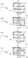
- a power capacitor may comprise a plurality of capacitor elements which are electrically connected in parallel and in series. As depicted in Fig. 1a , each such capacitor element comprises two electrode layers 19 and 21 and an intermediate dielectric layer 23. The dielectric layer 23 is thus arranged between the two electrode layers 19 and 21. The dielectric layer 23 may for example comprise a polymer material.
- the capacitor elements are wound so that a great plurality of turns of the two electrode layers and the dielectric layer are obtained.
- the capacitor elements can be arranged in a stacked manner forming an active package inside an enclosure or casing of the power capacitor. Inside the enclosure, the active package is immersed in a liquid capable to penetrate the polymer materials.
- Fig. 1a the capacitor element is shown during a zero-crossing, i.e. when the voltage applied across the two electrodes 19 and 21 is zero.
- a voltage is applied to the two electrodes 19 and 21 of the power capacitor, as shown in Fig. 1b , an attractive force, Coulomb force, is generated across the dielectric layer 23 between the two electrodes 19 and 21 because the two electrodes have different electric potential.
- This attractive force indicated by arrow 17, and also by the arrows between the electrode layers, is simultaneously acting on each turn of the power capacitor. This force will deform the soft dielectric material between the electrodes.
- the total deformation of the active package is the sum of the deformation across all of the turns of all the capacitor elements.
- the power capacitor comprises at least two capacitor elements which are composed of electrodes separated by one or more dielectrics.
- the capacitor elements are arranged in a row to form a capacitor package.
- At least one spring element is arranged between a pair of adjacent capacitor elements in the row or fixed at the outside of the capacitor element at one end of the row. The stiffness of the spring element is adapted such that the external vibrations of the capacitor are reduced. This results in a reduced sound radiation from the capacitor.
- WO2014202446 discloses a capacitor device which has a plurality of capacitor elements arranged in rows or stacked. Each capacitor element has two electrodes and a dielectric material arranged between the electrodes. There is between each pair of adjacent capacitor elements a damping element for attenuating vibrations caused by the electrodes.
- the spring element and the damping elements in the prior art occupy space inside the enclosure of the power capacitor while not contributing to the capacitance of the power capacitor.
- an object of the present disclosure is to provide a power capacitor which solves, or at least mitigates, the problems of the prior art.
- a power capacitor comprising: a casing, a first bushing, a second bushing or an earthing stud having the same electric potential as the casing, wherein the first bushing and the second bushing extend through the casing, a dielectric liquid, and a plurality of wound capacitor elements, each wound capacitor element comprising: a first electrode comprising two first layers of electrically conducting material connected to the first bushing, the two first layers being arranged movable towards and from each other, a second electrode comprising two second layers of electrically conducting material connected to the second bushing or to the earthing stud, the two second layers being arranged movable towards and from each other, and a dielectric layer arranged between the first electrode and the second electrode, wherein the two first layers, the two second layers and the dielectric layer are together wound in a plurality of turns to obtain a plurality of layers of the first electrode, of the second electrode and of the dielectric layer, wherein the wound capacitor elements are arranged in a stacked manner in the casing, adjacent wound capacitor elements
- Attenuation of the oscillations of the first electrode and the second electrode may thereby be obtained.
- This may in particular be obtained by the electrode configuration where each of the first electrode and the second electrode comprises two distinct layers of electrically conducting material extending parallel with each other turn by turn.
- the first electrode and the second electrode will still be attracted through the dielectric, but the repulsion of the two layers of each electrode, due to being on the same voltage potential, counteracts the electrode movement as the voltage alternates. The vibrations will therefore essentially cancel and attenuation of sound can thereby be obtained.
- the sound attenuation is hence obtained solely due to the dual-layered configuration of the first electrode and the dual-layered configuration of the second electrode.
- the two first layers have the same layer thickness.
- the two second layers have the same layer thickness.
- each of the two first layers is a conducting foil.
- the two first layers of conducting foil are arranged in a layered manner and wound together with the two second layers and the dielectric layer.
- Each conducting foil may for example be made of aluminium.
- Each conducting foil may according to one example comprise a zinc alloy.
- the conducting foils may beneficially be made very thin, so that their total thickness corresponds to the thickness of a standard electrode foil of a power capacitor.
- each of the two first layers is a metallisation layer provided on a respective side of a film.
- the first electrode may comprise a double-metallised film.
- Each metallised layer of the double-metallised film defines a respective one of the two first layers of electrically conducting material of the first electrode.
- the film may for example be a suitably soft polymer film.
- the metallisation to obtain the two first layers of electrically conducting material may for example be obtained by electroplating, spraying or physical vapour deposition (PVD).
- each of the two second layers is a conducting foil.
- the two second layers of conducting foil are arranged in a layered manner and wound together with the two first layers and the dielectric layer.
- Each conducting foil may for example be made of aluminium.
- Each conducting foil may according to one example comprise a zinc alloy.
- the conducting foils may beneficially be made very thin, so that their total thickness corresponds to the thickness of a standard electrode foil of a power capacitor.
- each of the two second layers is a metallisation layer provided on a respective side of a film.
- the second electrode may comprise a double-metallised film.
- Each metallised layer of the double-metallised film defines a respective one of the two second layers of electrically conducting material of the second electrode.
- the film may for example be a suitably polymer film.
- the metallisation to obtain the two second layers of electrically conducting material may for example be obtained by electroplating, spraying or PVD.
- the first electrode comprises exactly two first layers of electrically conducting material.
- the second electrode comprises exactly two second layers of electrically conducting material.
- Fig. 2 shows an example of a power capacitor 1.
- the power capacitor 1 comprises a casing, tank or enclosure 3, a first bushing 5 and a second bushing 7.
- the power capacitor could be provided with an earthing stud.
- the earthing stud generally has the same electric potential as the casing.
- the first bushing 5 penetrates the casing 3.
- the first bushing 5 hence extends through the casing 3.
- the second bushing 7 penetrates the casing 3.
- the second bushing 7 hence extends through the casing 3.
- the power capacitor 1 furthermore comprises a plurality of wound capacitor elements 9.
- the wound capacitor elements 9 are arranged in a stacked manner.
- the wound capacitor elements 9 are arranged in direct contact with each other. Adjacent wound capacitor elements 9 are hence in direct mechanical contact.
- the wound capacitor elements 9 are electrically connected to each other. They may for example be series connected and/or parallel connected. Each wound capacitor element 9 is electrically connected to the first bushing 5 and to the second bushing 7, as will be described in more detail below. As an alternative to being electrically connected to the second bushing, each wound capacitor element may instead be electrically connected to an earthing stud.
- the power capacitor 1 comprises a dielectric liquid.
- the dielectric liquid may for example be oil or an ester.
- the stacked wound capacitor elements 9 are immersed in the dielectric liquid.
- the dielectric liquid hence penetrates the dielectric material to improve the performance thereof and fills out all voids or empty spaces inside the casing 3.
- Each wound capacitor element 9 comprises a first electrode 11 and a second electrode 13.
- the first electrode 11 comprises two first layers 11a and 11b of electrically conducting material.
- the two first layers 11a and 11b of the first electrode 11 are arranged in a layered configuration.
- the two first layers 11a and 11b are arranged parallel with each other for each turn of the wound capacitor element 9.
- the first electrode 11 may beneficially comprise exactly two first layers 11a and 11b.
- the first electrode may comprise more than two first layers of electrically conducting material.
- the two first layers 11a and 11b are both electrically connected to the first bushing 5.
- the two first layers 11a and 11b hence have the same electric potential.
- the two first layers 11a and 11b are configured to be movable towards each other and away from each other in the wound state of the wound capacitor element 9. This possible movement between the two first layers 11a and 11b provides vibration attenuation, as will be described in more detail in the following.
- the first electrode 11 may according to one example comprise two electrically conducting foils arranged extending parallel to each other.
- the two electrically conducting foils form a respective one of the two first layers 11a and 11b of electrically conducting material.
- the electrically conducting foils are beneficially made as thin as possible so that their total thickness is essentially the same as the thickness of a traditional foil electrode.
- the first electrode 11 may comprise a double-metallised film. In this case, each metallisation surface of the double-metallised film forms a respective one of the two first layers 11a and 11b.
- the thickness dimension of the film is compressible and allows for movement of the two metallisation surface towards each other and away from each other when the wound capacitor element is energised.
- the second electrode 13 comprises two second layers 13a and 13b of electrically conducting material, as shown in for example Fig. 3 .
- the two second layers 13a and 13b of the second electrode 13 are arranged in a layered configuration.
- the two second layers 13a and 13b are arranged parallel with each other for each turn of the wound capacitor element 9.
- the second electrode 13 may beneficially comprise exactly two second layers 13a and 13b.
- the second electrode may comprise more than two second layers of electrically conducting material.
- the two second layers 13a and 13b are both electrically connected to the second bushing 7. Alternatively, the two second layers may be electrically connected to an earthing stud.
- the two second layers 13a and 13b hence have the same electric potential.
- the two second layers 13a and 13b are configured to be movable towards each other and away from each other in the wound state of the wound capacitor element 9. This possible movement between the two second layers 13a and 13b provides vibration attenuation.
- the second electrode 13 may according to one example comprise two electrically conducting foils arranged extending parallel to each other.
- the two electrically conducting foils form a respective one of the two second layers 13a and 13b of electrically conducting material.
- the electrically conducting foils are beneficially made as thin as possible so that their total thickness is essentially the same as the thickness of a traditional foil electrode.
- the second electrode 13 may comprise a double-metallised film.
- each metallisation surface of the double-metallised film forms a respective one of the two second layers 13a and 13b.
- the thickness dimension of the film is compressible and allows for movement of the two metallisation surface towards each other and away from each other when the wound capacitor element is energised.
- the wound capacitor element 9 comprises a dielectric layer 15.
- the dielectric layer 15 may for example comprise a polymeric material or any other suitable electrically insulating material, such as a cellulose-based material.
- the dielectric layer 15 is arranged between the first electrode 11 and the second electrode 13.
- the first electrode 11, the dielectric layer 15 and the second electrode 13 are hence arranged parallel to each other in a sandwiched configuration.
- the first electrode 11, the dielectric layer 15 and the second electrode 13 are together wound to form the wound power capacitor element 9. In this manner, a plurality of instances or layers of the first electrode 11, the second electrode 13 and the dielectric layer 15 is provided.
- the wound capacitor element 8 may be flattened, as shown in Fig. 2 , to take up less space in the casing 3.
- Fig. 4a the voltage applied to the power capacitor 1 is at a zero-crossing, and thus the potential is zero at both the first electrode 11 and the second electrode 13. In this case, there is no attractive force between the first electrode 11 and the second electrode 13.
- Fig. 4b shows a situation where the first electrode 11 has a positive electric potential. This is illustrated by the arrow on the sinusoidal duty cycle of the alternating voltage. Due to Coulomb's attraction F, in for example, the uppermost layer of the dielectric layer 15, the layer 11a of the first electrode 11 is attracted to the layer 13b arranged on the opposite side of the dielectric layer 15. However, since the layer 13b at the same time is at the same electric potential as the adjacently arranged layer 13a, they will repel each other. This repelling movement between the two second layers 13a and 13b causes a compensation of the attracting movement between the layer 11a and the layer 13b. This causes a cancellation, or at least reduction, of the movement, speed and acceleration at the outermost turn.
- Fig. 4d the voltage applied to the power capacitor 1 is in the negative phase of the sinusoidal duty cycle.
- the sign of the voltage potential across the first electrode 11 and the second electrode 13 has thus shifted compared to the case illustrated in Fig. 4b but the effect will be the same as described with reference to Fig. 4b .
Landscapes
- Engineering & Computer Science (AREA)
- Power Engineering (AREA)
- Manufacturing & Machinery (AREA)
- Microelectronics & Electronic Packaging (AREA)
- Chemical & Material Sciences (AREA)
- Materials Engineering (AREA)
- Fixed Capacitors And Capacitor Manufacturing Machines (AREA)
Abstract
Description
- The present disclosure generally relates to power capacitors. In particular it relates to a power capacitor that provides vibration attenuation.
- A power capacitor may comprise a plurality of capacitor elements which are electrically connected in parallel and in series. As depicted in
Fig. 1a , each such capacitor element comprises twoelectrode layers dielectric layer 23. Thedielectric layer 23 is thus arranged between the twoelectrode layers dielectric layer 23 may for example comprise a polymer material. The capacitor elements are wound so that a great plurality of turns of the two electrode layers and the dielectric layer are obtained. The capacitor elements can be arranged in a stacked manner forming an active package inside an enclosure or casing of the power capacitor. Inside the enclosure, the active package is immersed in a liquid capable to penetrate the polymer materials. - In
Fig. 1a , the capacitor element is shown during a zero-crossing, i.e. when the voltage applied across the twoelectrodes electrodes Fig. 1b , an attractive force, Coulomb force, is generated across thedielectric layer 23 between the twoelectrodes arrow 17, and also by the arrows between the electrode layers, is simultaneously acting on each turn of the power capacitor. This force will deform the soft dielectric material between the electrodes. The total deformation of the active package is the sum of the deformation across all of the turns of all the capacitor elements. When the voltage crosses the next zero-crossing, the attractive force will become zero as shown inFig. 1c . When the voltage potential is reversed, charges on theelectrodes Fig. 1d . This gives rise to a mechanical movement between the electrode layers causing them to oscillate at a frequency twice the frequency of the applied alternating voltage. Since the stack of capacitor elements is immersed in liquid, the vibrations of the capacitor elements are transferred to the capacitor enclosure. The surface vibrations of the enclosure will generate undesirable sound in the form of audible noise. - An example of a power capacitor with noise reduction capabilities is disclosed in
EP 0 701 263 B1 -
WO2014202446 discloses a capacitor device which has a plurality of capacitor elements arranged in rows or stacked. Each capacitor element has two electrodes and a dielectric material arranged between the electrodes. There is between each pair of adjacent capacitor elements a damping element for attenuating vibrations caused by the electrodes. - The spring element and the damping elements in the prior art occupy space inside the enclosure of the power capacitor while not contributing to the capacitance of the power capacitor.
- In view of the above, an object of the present disclosure is to provide a power capacitor which solves, or at least mitigates, the problems of the prior art.
- There is hence provided a power capacitor comprising: a casing, a first bushing, a second bushing or an earthing stud having the same electric potential as the casing, wherein the first bushing and the second bushing extend through the casing, a dielectric liquid, and a plurality of wound capacitor elements, each wound capacitor element comprising: a first electrode comprising two first layers of electrically conducting material connected to the first bushing, the two first layers being arranged movable towards and from each other, a second electrode comprising two second layers of electrically conducting material connected to the second bushing or to the earthing stud, the two second layers being arranged movable towards and from each other, and a dielectric layer arranged between the first electrode and the second electrode, wherein the two first layers, the two second layers and the dielectric layer are together wound in a plurality of turns to obtain a plurality of layers of the first electrode, of the second electrode and of the dielectric layer, wherein the wound capacitor elements are arranged in a stacked manner in the casing, adjacent wound capacitor elements being in direct contact with each other, and wherein the capacitor elements are submerged in the dielectric liquid.
- Attenuation of the oscillations of the first electrode and the second electrode may thereby be obtained. This may in particular be obtained by the electrode configuration where each of the first electrode and the second electrode comprises two distinct layers of electrically conducting material extending parallel with each other turn by turn. The first electrode and the second electrode will still be attracted through the dielectric, but the repulsion of the two layers of each electrode, due to being on the same voltage potential, counteracts the electrode movement as the voltage alternates. The vibrations will therefore essentially cancel and attenuation of sound can thereby be obtained.
- The sound attenuation is hence obtained solely due to the dual-layered configuration of the first electrode and the dual-layered configuration of the second electrode.
- According to one embodiment the two first layers have the same layer thickness.
- By providing the two first layers of electrically conducting material with the same thickness better vibration cancellation may be obtained.
- According to one embodiment the two second layers have the same layer thickness.
- By providing the two second layers of electrically conducting material with the same thickness better vibration cancellation may be obtained.
- According to one embodiment each of the two first layers is a conducting foil.
- The two first layers of conducting foil are arranged in a layered manner and wound together with the two second layers and the dielectric layer.
- Each conducting foil may for example be made of aluminium.
- Each conducting foil may according to one example comprise a zinc alloy.
- The conducting foils may beneficially be made very thin, so that their total thickness corresponds to the thickness of a standard electrode foil of a power capacitor.
- According to one embodiment each of the two first layers is a metallisation layer provided on a respective side of a film. To this end, the first electrode may comprise a double-metallised film. Each metallised layer of the double-metallised film defines a respective one of the two first layers of electrically conducting material of the first electrode. The film may for example be a suitably soft polymer film.
- The metallisation to obtain the two first layers of electrically conducting material may for example be obtained by electroplating, spraying or physical vapour deposition (PVD).
- According to one embodiment each of the two second layers is a conducting foil.
- The two second layers of conducting foil are arranged in a layered manner and wound together with the two first layers and the dielectric layer.
- Each conducting foil may for example be made of aluminium.
- Each conducting foil may according to one example comprise a zinc alloy.
- The conducting foils may beneficially be made very thin, so that their total thickness corresponds to the thickness of a standard electrode foil of a power capacitor.
- According to one embodiment each of the two second layers is a metallisation layer provided on a respective side of a film. To this end, the second electrode may comprise a double-metallised film. Each metallised layer of the double-metallised film defines a respective one of the two second layers of electrically conducting material of the second electrode. The film may for example be a suitably polymer film.
- The metallisation to obtain the two second layers of electrically conducting material may for example be obtained by electroplating, spraying or PVD.
- According to one embodiment the first electrode comprises exactly two first layers of electrically conducting material.
- According to one embodiment the second electrode comprises exactly two second layers of electrically conducting material.
- It is beneficial to use only two first layers of electrically conducting material because in this manner the cancellation effect of the vibrations may be obtained while the material cost and the size of the wound capacitor element may be kept low. Additional layers of electrically conducting material does not contribute to the capacitance of the power capacitor, and therefore exactly two first layers and exactly two second layers is considered to be optimal to achieve maximal sound attenuation with minimal loss of capacitance per volume of the power capacitor.
- Generally, all terms used in the claims are to be interpreted according to their ordinary meaning in the technical field, unless explicitly defined otherwise herein. All references to a/an/the element, apparatus, component, means, etc. are to be interpreted openly as referring to at least one instance of the element, apparatus, component, means, etc., unless explicitly stated otherwise.
- The specific embodiments of the inventive concept will now be described, by way of example, with reference to the accompanying drawings, in which:
-
Figs 1a-1d schematically shows the generation of vibrations in prior art power capacitors; -
Fig. 2 shows a perspective view of an example of a power capacitor; -
Fig. 3 shows a wound capacitor element; and -
Figs 4a-4d show simplified cross-sectional views of a wound capacitor element in four stages during an alternating voltage duty cycle. - The inventive concept will now be described more fully hereinafter with reference to the accompanying drawings, in which exemplifying embodiments are shown. The inventive concept may, however, be embodied in many different forms and should not be construed as limited to the embodiments set forth herein; rather, these embodiments are provided by way of example so that this disclosure will be thorough and complete, and will fully convey the scope of the inventive concept to those skilled in the art. Like numbers refer to like elements throughout the description.
-
Fig. 2 shows an example of apower capacitor 1. Thepower capacitor 1 comprises a casing, tank orenclosure 3, afirst bushing 5 and asecond bushing 7. - As an alternative to a second bushing, the power capacitor could be provided with an earthing stud. In this case, the earthing stud generally has the same electric potential as the casing.
- The
first bushing 5 penetrates thecasing 3. Thefirst bushing 5 hence extends through thecasing 3. - The
second bushing 7 penetrates thecasing 3. Thesecond bushing 7 hence extends through thecasing 3. - The
power capacitor 1 furthermore comprises a plurality ofwound capacitor elements 9. Thewound capacitor elements 9 are arranged in a stacked manner. Thewound capacitor elements 9 are arranged in direct contact with each other. Adjacentwound capacitor elements 9 are hence in direct mechanical contact. - The
wound capacitor elements 9 are electrically connected to each other. They may for example be series connected and/or parallel connected. Eachwound capacitor element 9 is electrically connected to thefirst bushing 5 and to thesecond bushing 7, as will be described in more detail below. As an alternative to being electrically connected to the second bushing, each wound capacitor element may instead be electrically connected to an earthing stud. - The
power capacitor 1 comprises a dielectric liquid. The dielectric liquid may for example be oil or an ester. The stackedwound capacitor elements 9 are immersed in the dielectric liquid. The dielectric liquid hence penetrates the dielectric material to improve the performance thereof and fills out all voids or empty spaces inside thecasing 3. - With reference to
Fig. 3 , an example of awound capacitor element 9 is shown. Eachwound capacitor element 9 comprises afirst electrode 11 and asecond electrode 13. - The
first electrode 11 comprises twofirst layers first layers first electrode 11 are arranged in a layered configuration. The twofirst layers wound capacitor element 9. Thefirst electrode 11 may beneficially comprise exactly twofirst layers - The two
first layers first bushing 5. The twofirst layers first layers wound capacitor element 9. This possible movement between the twofirst layers - The
first electrode 11 may according to one example comprise two electrically conducting foils arranged extending parallel to each other. The two electrically conducting foils form a respective one of the twofirst layers first electrode 11 may comprise a double-metallised film. In this case, each metallisation surface of the double-metallised film forms a respective one of the twofirst layers - The
second electrode 13 comprises twosecond layers Fig. 3 . The twosecond layers second electrode 13 are arranged in a layered configuration. The twosecond layers wound capacitor element 9. Thesecond electrode 13 may beneficially comprise exactly twosecond layers - The two
second layers second bushing 7. Alternatively, the two second layers may be electrically connected to an earthing stud. The twosecond layers second layers wound capacitor element 9. This possible movement between the twosecond layers - The
second electrode 13 may according to one example comprise two electrically conducting foils arranged extending parallel to each other. The two electrically conducting foils form a respective one of the twosecond layers second electrode 13 may comprise a double-metallised film. In this case, each metallisation surface of the double-metallised film forms a respective one of the twosecond layers - The
wound capacitor element 9 comprises adielectric layer 15. Thedielectric layer 15 may for example comprise a polymeric material or any other suitable electrically insulating material, such as a cellulose-based material. Thedielectric layer 15 is arranged between thefirst electrode 11 and thesecond electrode 13. Thefirst electrode 11, thedielectric layer 15 and thesecond electrode 13 are hence arranged parallel to each other in a sandwiched configuration. Thefirst electrode 11, thedielectric layer 15 and thesecond electrode 13 are together wound to form the woundpower capacitor element 9. In this manner, a plurality of instances or layers of thefirst electrode 11, thesecond electrode 13 and thedielectric layer 15 is provided. The wound capacitor element 8 may be flattened, as shown inFig. 2 , to take up less space in thecasing 3. - The
power capacitor 1 will now be described in operation with reference toFigs 4a-4c. Fig. 4a the voltage applied to thepower capacitor 1 is at a zero-crossing, and thus the potential is zero at both thefirst electrode 11 and thesecond electrode 13. In this case, there is no attractive force between thefirst electrode 11 and thesecond electrode 13. -
Fig. 4b shows a situation where thefirst electrode 11 has a positive electric potential. This is illustrated by the arrow on the sinusoidal duty cycle of the alternating voltage. Due to Coulomb's attraction F, in for example, the uppermost layer of thedielectric layer 15, thelayer 11a of thefirst electrode 11 is attracted to thelayer 13b arranged on the opposite side of thedielectric layer 15. However, since thelayer 13b at the same time is at the same electric potential as the adjacently arrangedlayer 13a, they will repel each other. This repelling movement between the twosecond layers layer 11a and thelayer 13b. This causes a cancellation, or at least reduction, of the movement, speed and acceleration at the outermost turn. - In the situation shown in
Fig. 4c , the voltage applied to thewound capacitor element 9 crosses zero again. Thefirst electrode 11 and thesecond electrode 13 is thus at the same electric potential. In the absence of the attractive force between thefirst electrode 11 and thesecond electrode 13, thedielectric material 15 will relax, causing thefirst electrode 11 and thesecond electrode 13 to move away from each other. The total cross-sectional dimension of thewound capacitor element 9 will remain essentially unchanged compared to the situation shown inFig. 4b . - In
Fig. 4d the voltage applied to thepower capacitor 1 is in the negative phase of the sinusoidal duty cycle. The sign of the voltage potential across thefirst electrode 11 and thesecond electrode 13 has thus shifted compared to the case illustrated inFig. 4b but the effect will be the same as described with reference toFig. 4b . - In this manner, the vibrations of the
first electrode 11 and thesecond electrode 13 are partly cancelled and there will consequently be an attenuation of sound emitted by thepower capacitor 1. - The inventive concept has mainly been described above with reference to a few examples. However, as is readily appreciated by a person skilled in the art, other embodiments than the ones disclosed above are equally possible within the scope of the inventive concept, as defined by the appended claims.
Claims (9)
- A power capacitor (1) comprising:- a casing (3),- a first bushing (5),- a second bushing (7) or an earthing stud having the same electric potential as the casing (3),wherein the first bushing (5) and the second bushing (7) extend through the casing (3),- a dielectric liquid, and- a plurality of wound capacitor elements (9), each wound capacitor element (9) comprising:wherein the wound capacitor elements (9) are arranged in a stacked manner in the casing (3), adjacent wound capacitor elements (9) being in direct contact with each other, and wherein the capacitor elements (9) are submerged in the dielectric liquid.a first electrode (11) comprising two first layers (11a, 11b) of electrically conducting material connected to the first bushing (5), the two first layers being arranged movable towards and from each other,a second electrode (13) comprising two second layers (13a, 13b) of electrically conducting material connected to the second bushing (7) or to the earthing stud, the two second layers (13a, 13b) being arranged movable towards and from each other, anda dielectric layer (15) arranged between the first electrode (11) and the second electrode (13),wherein the two first layers (11a, 11b), the two second layers (13a, 13b) and the dielectric layer (15) are together wound in a plurality of turns to obtain a plurality of layers of the first electrode (11), of the second electrode (13) and of the dielectric layer (15),
- The power capacitor (1) as claimed in claim 1, wherein the two first layers (11a, 11b) have the same layer thickness.
- The power capacitor (1) as claimed in claim 1 or 2, wherein the two second layers (13a, 13b) have the same layer thickness.
- The power capacitor (1) as claimed in any of the preceding claims, wherein each of the two first layers (11a, 11b) is a conducting foil.
- The power capacitor (1) as claimed in any of claims 1-3, wherein each of the two first layers (11a, 11b) is a metallisation layer provided on a respective side of a film.
- The power capacitor (1) as claimed in any of the preceding claims, wherein each of the two second layers (13a, 13b) is a conducting foil.
- The power capacitor (1) as claimed in claim 1-5, wherein each of the two second layers (13a, 13b) is a metallisation layer provided on a respective side of a film.
- The power capacitor (1) as claimed in any of the preceding claims, wherein the first electrode (11) comprises exactly two first layers (11a, 11b) of electrically conducting material.
- The power capacitor (1) as claimed in any of the preceding claims, wherein the second electrode (13) comprises exactly two second layers (13a, 13b) of electrically conducting material.
Priority Applications (6)
| Application Number | Priority Date | Filing Date | Title |
|---|---|---|---|
| EP17168209.9A EP3396690B1 (en) | 2017-04-26 | 2017-04-26 | Multielectrode power capacitor with reduce noise vibration |
| BR112019021200-0A BR112019021200B1 (en) | 2017-04-26 | 2018-04-25 | MULTIELECTRODE POWER CAPACITOR WITH REDUCED NOISE VIBRATION |
| US16/606,511 US10658119B1 (en) | 2017-04-26 | 2018-04-25 | Multielectrode power capacitor with reduce noise vibration |
| PCT/EP2018/060512 WO2018197522A1 (en) | 2017-04-26 | 2018-04-25 | Multielectrode power capacitor with reduce noise vibration |
| KR1020197033176A KR102121162B1 (en) | 2017-04-26 | 2018-04-25 | Multi-electrode power capacitor with reduced noise vibration |
| CN201880027312.8A CN110546724B (en) | 2017-04-26 | 2018-04-25 | Multi-electrode power capacitors with reduced noise vibration |
Applications Claiming Priority (1)
| Application Number | Priority Date | Filing Date | Title |
|---|---|---|---|
| EP17168209.9A EP3396690B1 (en) | 2017-04-26 | 2017-04-26 | Multielectrode power capacitor with reduce noise vibration |
Publications (2)
| Publication Number | Publication Date |
|---|---|
| EP3396690A1 true EP3396690A1 (en) | 2018-10-31 |
| EP3396690B1 EP3396690B1 (en) | 2020-04-01 |
Family
ID=58632887
Family Applications (1)
| Application Number | Title | Priority Date | Filing Date |
|---|---|---|---|
| EP17168209.9A Active EP3396690B1 (en) | 2017-04-26 | 2017-04-26 | Multielectrode power capacitor with reduce noise vibration |
Country Status (6)
| Country | Link |
|---|---|
| US (1) | US10658119B1 (en) |
| EP (1) | EP3396690B1 (en) |
| KR (1) | KR102121162B1 (en) |
| CN (1) | CN110546724B (en) |
| BR (1) | BR112019021200B1 (en) |
| WO (1) | WO2018197522A1 (en) |
Families Citing this family (1)
| Publication number | Priority date | Publication date | Assignee | Title |
|---|---|---|---|---|
| CN113690055A (en) * | 2021-08-18 | 2021-11-23 | 国网河南省电力公司漯河供电公司 | Filter capacitor noise reduction device |
Citations (7)
| Publication number | Priority date | Publication date | Assignee | Title |
|---|---|---|---|---|
| US3593072A (en) * | 1969-11-19 | 1971-07-13 | Trw Inc | Metallized capacitor |
| US3715784A (en) * | 1971-01-08 | 1973-02-13 | C Rayburn | Method of making a miniature metalized capacitor |
| DE3148360A1 (en) * | 1981-12-07 | 1983-06-09 | Andreas Dr.-Ing. 5063 Overath Daszkowski | High-voltage capacitor comprising foils in the form of metallised plastic films or metallised paper and coated with a semiconducting layer |
| EP1801824A1 (en) * | 2005-12-23 | 2007-06-27 | ABB Research Ltd | A film, an electrode configuration, a bushing and a method of using an electrode configuration or a bushing |
| JP2012009654A (en) * | 2010-06-25 | 2012-01-12 | Daikin Ind Ltd | Film capacitor |
| JP2013239624A (en) * | 2012-05-16 | 2013-11-28 | Honda Motor Co Ltd | Capacitor module |
| WO2014080411A1 (en) * | 2012-11-26 | 2014-05-30 | Celem Passive Components Ltd. | A wound film capacitor with improved heat evacuation |
Family Cites Families (16)
| Publication number | Priority date | Publication date | Assignee | Title |
|---|---|---|---|---|
| DE2015372A1 (en) * | 1970-04-01 | 1972-02-24 | Boussange A | capacitor |
| US4348712A (en) * | 1978-10-18 | 1982-09-07 | General Electric Company | Capacitor with embossed electrodes |
| US4228481A (en) * | 1978-10-19 | 1980-10-14 | General Electric Company | Capacitor with embossed foil electrode |
| US4422962A (en) * | 1981-02-19 | 1983-12-27 | General Electric Company | Polyglycol dielectric capacitor fluid |
| US4464700A (en) * | 1981-12-17 | 1984-08-07 | Asea Aktiebolag | Power capacitor |
| SE503305C2 (en) | 1994-06-21 | 1996-05-13 | Asea Brown Boveri | Capacitor |
| EP1724796A3 (en) * | 1998-12-05 | 2014-04-09 | CAP-XX Limited | A charge storage device |
| US20050019652A1 (en) * | 2003-07-21 | 2005-01-27 | Fauteux Denis G. | Electrode assembly and method of manufacturing same |
| DE102004038863B3 (en) | 2004-08-10 | 2006-04-06 | Westermann, Wolfgang | Metallized plastic film capacitor and use of a metallized plastic film capacitor |
| FR2890785A1 (en) * | 2005-09-15 | 2007-03-16 | Batscap Sa | DEVICE FOR STORING ELECTRIC ENERGY COMPRISING A BARRIER LAYER FOR PROTECTING THE COLLECTOR |
| EP2443639B1 (en) * | 2009-06-16 | 2017-09-27 | High Energy Corp. | Sealed and impregnated wound capacitor assemblies |
| KR101062607B1 (en) * | 2009-12-28 | 2011-09-06 | 주식회사 효성 | Power transformer |
| US10366836B2 (en) | 2010-05-26 | 2019-07-30 | Kemet Electronics Corporation | Electronic component structures with reduced microphonic noise |
| US20120229948A1 (en) * | 2011-03-11 | 2012-09-13 | S B E, Inc. | Capacitor Used as Insulating Spacer for a High Current Bus Structure |
| CN102522198B (en) | 2011-12-08 | 2013-07-24 | 华中科技大学 | Metallized membrane capacitor assembly |
| DE102013211699A1 (en) | 2013-06-20 | 2014-12-24 | Siemens Aktiengesellschaft | capacitor device |
-
2017
- 2017-04-26 EP EP17168209.9A patent/EP3396690B1/en active Active
-
2018
- 2018-04-25 BR BR112019021200-0A patent/BR112019021200B1/en active IP Right Grant
- 2018-04-25 KR KR1020197033176A patent/KR102121162B1/en active Active
- 2018-04-25 WO PCT/EP2018/060512 patent/WO2018197522A1/en not_active Ceased
- 2018-04-25 US US16/606,511 patent/US10658119B1/en active Active
- 2018-04-25 CN CN201880027312.8A patent/CN110546724B/en active Active
Patent Citations (7)
| Publication number | Priority date | Publication date | Assignee | Title |
|---|---|---|---|---|
| US3593072A (en) * | 1969-11-19 | 1971-07-13 | Trw Inc | Metallized capacitor |
| US3715784A (en) * | 1971-01-08 | 1973-02-13 | C Rayburn | Method of making a miniature metalized capacitor |
| DE3148360A1 (en) * | 1981-12-07 | 1983-06-09 | Andreas Dr.-Ing. 5063 Overath Daszkowski | High-voltage capacitor comprising foils in the form of metallised plastic films or metallised paper and coated with a semiconducting layer |
| EP1801824A1 (en) * | 2005-12-23 | 2007-06-27 | ABB Research Ltd | A film, an electrode configuration, a bushing and a method of using an electrode configuration or a bushing |
| JP2012009654A (en) * | 2010-06-25 | 2012-01-12 | Daikin Ind Ltd | Film capacitor |
| JP2013239624A (en) * | 2012-05-16 | 2013-11-28 | Honda Motor Co Ltd | Capacitor module |
| WO2014080411A1 (en) * | 2012-11-26 | 2014-05-30 | Celem Passive Components Ltd. | A wound film capacitor with improved heat evacuation |
Also Published As
| Publication number | Publication date |
|---|---|
| US10658119B1 (en) | 2020-05-19 |
| CN110546724A (en) | 2019-12-06 |
| EP3396690B1 (en) | 2020-04-01 |
| CN110546724B (en) | 2020-11-10 |
| KR102121162B1 (en) | 2020-06-10 |
| BR112019021200A2 (en) | 2020-04-28 |
| WO2018197522A1 (en) | 2018-11-01 |
| BR112019021200A8 (en) | 2022-12-13 |
| KR20190130047A (en) | 2019-11-20 |
| US20200135405A1 (en) | 2020-04-30 |
| BR112019021200B1 (en) | 2024-02-06 |
Similar Documents
| Publication | Publication Date | Title |
|---|---|---|
| KR102064008B1 (en) | Multi-layered capacitor and circuit board mounted multi-layered capacitor | |
| KR101548773B1 (en) | Mounting structure of ciruit board having thereon multi-layered ceramic capacitor | |
| US9390853B2 (en) | Multilayer ceramic capacitor and mounting board therefor | |
| JP5267363B2 (en) | Multilayer electronic components | |
| JP2012216864A (en) | Mounting structure and method of circuit board for multi-layered ceramic capacitor, land pattern of circuit board, packing unit for multi-layered ceramic capacitor, and aligning method | |
| US9460851B2 (en) | Multilayer ceramic electronic component and board having the same | |
| US20190103221A1 (en) | Multilayer electronic component and board having the same | |
| JP2012248846A (en) | Mounting structure of circuit board of multilayer ceramic capacitor | |
| US10403433B2 (en) | Multilayer electronic component | |
| US10770235B2 (en) | Multilayer capacitor | |
| KR20160051309A (en) | Multi-layered ceramic electronic components and board having the same mounted thereon | |
| KR102730020B1 (en) | Multilayered electronic component and board having the same mounted thereon | |
| CN109427482A (en) | Composite electronic assembly and board having the same | |
| KR101548769B1 (en) | Multi-layered capacitor and manufacturing method thereof | |
| KR20150089277A (en) | Multi-layered ceramic electroic components and mounting circuit thereof | |
| JP5974653B2 (en) | How to use multilayer capacitors | |
| KR20170024750A (en) | Multilayer capacitor and board having the same | |
| US20160307700A1 (en) | Capacitor component and board having the same | |
| KR102059442B1 (en) | Composite electronic component and board for mounting the same | |
| CN110880417A (en) | Ceramic electronic component | |
| KR101452074B1 (en) | Multi-layered ceramic capacitor and board for mounting the same | |
| KR101514562B1 (en) | Multi-layered ceramic electronic component and mounting circuit thereof | |
| US10658119B1 (en) | Multielectrode power capacitor with reduce noise vibration | |
| US20190198248A1 (en) | Multilayer capacitor, method of manufacturing the same, and board having the same | |
| JP2016178160A (en) | Laminated film capacitor |
Legal Events
| Date | Code | Title | Description |
|---|---|---|---|
| PUAI | Public reference made under article 153(3) epc to a published international application that has entered the european phase |
Free format text: ORIGINAL CODE: 0009012 |
|
| STAA | Information on the status of an ep patent application or granted ep patent |
Free format text: STATUS: THE APPLICATION HAS BEEN PUBLISHED |
|
| AK | Designated contracting states |
Kind code of ref document: A1 Designated state(s): AL AT BE BG CH CY CZ DE DK EE ES FI FR GB GR HR HU IE IS IT LI LT LU LV MC MK MT NL NO PL PT RO RS SE SI SK SM TR |
|
| AX | Request for extension of the european patent |
Extension state: BA ME |
|
| STAA | Information on the status of an ep patent application or granted ep patent |
Free format text: STATUS: REQUEST FOR EXAMINATION WAS MADE |
|
| STAA | Information on the status of an ep patent application or granted ep patent |
Free format text: STATUS: EXAMINATION IS IN PROGRESS |
|
| 17P | Request for examination filed |
Effective date: 20190430 |
|
| RBV | Designated contracting states (corrected) |
Designated state(s): AL AT BE BG CH CY CZ DE DK EE ES FI FR GB GR HR HU IE IS IT LI LT LU LV MC MK MT NL NO PL PT RO RS SE SI SK SM TR |
|
| 17Q | First examination report despatched |
Effective date: 20190528 |
|
| GRAP | Despatch of communication of intention to grant a patent |
Free format text: ORIGINAL CODE: EPIDOSNIGR1 |
|
| STAA | Information on the status of an ep patent application or granted ep patent |
Free format text: STATUS: GRANT OF PATENT IS INTENDED |
|
| RIC1 | Information provided on ipc code assigned before grant |
Ipc: H01G 4/008 20060101ALI20191009BHEP Ipc: H01G 4/00 20060101ALI20191009BHEP Ipc: H01G 4/232 20060101ALI20191009BHEP Ipc: H01G 4/32 20060101AFI20191009BHEP Ipc: H01G 4/224 20060101ALI20191009BHEP Ipc: H01G 4/38 20060101ALI20191009BHEP |
|
| INTG | Intention to grant announced |
Effective date: 20191031 |
|
| GRAS | Grant fee paid |
Free format text: ORIGINAL CODE: EPIDOSNIGR3 |
|
| GRAA | (expected) grant |
Free format text: ORIGINAL CODE: 0009210 |
|
| STAA | Information on the status of an ep patent application or granted ep patent |
Free format text: STATUS: THE PATENT HAS BEEN GRANTED |
|
| RAP1 | Party data changed (applicant data changed or rights of an application transferred) |
Owner name: ABB POWER GRIDS SWITZERLAND AG |
|
| AK | Designated contracting states |
Kind code of ref document: B1 Designated state(s): AL AT BE BG CH CY CZ DE DK EE ES FI FR GB GR HR HU IE IS IT LI LT LU LV MC MK MT NL NO PL PT RO RS SE SI SK SM TR |
|
| REG | Reference to a national code |
Ref country code: GB Ref legal event code: FG4D |
|
| REG | Reference to a national code |
Ref country code: CH Ref legal event code: EP Ref country code: AT Ref legal event code: REF Ref document number: 1252440 Country of ref document: AT Kind code of ref document: T Effective date: 20200415 |
|
| REG | Reference to a national code |
Ref country code: DE Ref legal event code: R096 Ref document number: 602017013833 Country of ref document: DE |
|
| REG | Reference to a national code |
Ref country code: IE Ref legal event code: FG4D |
|
| REG | Reference to a national code |
Ref country code: FI Ref legal event code: FGE |
|
| PG25 | Lapsed in a contracting state [announced via postgrant information from national office to epo] |
Ref country code: BG Free format text: LAPSE BECAUSE OF FAILURE TO SUBMIT A TRANSLATION OF THE DESCRIPTION OR TO PAY THE FEE WITHIN THE PRESCRIBED TIME-LIMIT Effective date: 20200701 |
|
| REG | Reference to a national code |
Ref country code: NL Ref legal event code: MP Effective date: 20200401 |
|
| REG | Reference to a national code |
Ref country code: LT Ref legal event code: MG4D |
|
| PG25 | Lapsed in a contracting state [announced via postgrant information from national office to epo] |
Ref country code: GR Free format text: LAPSE BECAUSE OF FAILURE TO SUBMIT A TRANSLATION OF THE DESCRIPTION OR TO PAY THE FEE WITHIN THE PRESCRIBED TIME-LIMIT Effective date: 20200702 Ref country code: NO Free format text: LAPSE BECAUSE OF FAILURE TO SUBMIT A TRANSLATION OF THE DESCRIPTION OR TO PAY THE FEE WITHIN THE PRESCRIBED TIME-LIMIT Effective date: 20200701 Ref country code: IS Free format text: LAPSE BECAUSE OF FAILURE TO SUBMIT A TRANSLATION OF THE DESCRIPTION OR TO PAY THE FEE WITHIN THE PRESCRIBED TIME-LIMIT Effective date: 20200801 Ref country code: NL Free format text: LAPSE BECAUSE OF FAILURE TO SUBMIT A TRANSLATION OF THE DESCRIPTION OR TO PAY THE FEE WITHIN THE PRESCRIBED TIME-LIMIT Effective date: 20200401 Ref country code: SE Free format text: LAPSE BECAUSE OF FAILURE TO SUBMIT A TRANSLATION OF THE DESCRIPTION OR TO PAY THE FEE WITHIN THE PRESCRIBED TIME-LIMIT Effective date: 20200401 Ref country code: LT Free format text: LAPSE BECAUSE OF FAILURE TO SUBMIT A TRANSLATION OF THE DESCRIPTION OR TO PAY THE FEE WITHIN THE PRESCRIBED TIME-LIMIT Effective date: 20200401 Ref country code: PT Free format text: LAPSE BECAUSE OF FAILURE TO SUBMIT A TRANSLATION OF THE DESCRIPTION OR TO PAY THE FEE WITHIN THE PRESCRIBED TIME-LIMIT Effective date: 20200817 |
|
| REG | Reference to a national code |
Ref country code: AT Ref legal event code: MK05 Ref document number: 1252440 Country of ref document: AT Kind code of ref document: T Effective date: 20200401 |
|
| PG25 | Lapsed in a contracting state [announced via postgrant information from national office to epo] |
Ref country code: RS Free format text: LAPSE BECAUSE OF FAILURE TO SUBMIT A TRANSLATION OF THE DESCRIPTION OR TO PAY THE FEE WITHIN THE PRESCRIBED TIME-LIMIT Effective date: 20200401 Ref country code: LV Free format text: LAPSE BECAUSE OF FAILURE TO SUBMIT A TRANSLATION OF THE DESCRIPTION OR TO PAY THE FEE WITHIN THE PRESCRIBED TIME-LIMIT Effective date: 20200401 Ref country code: HR Free format text: LAPSE BECAUSE OF FAILURE TO SUBMIT A TRANSLATION OF THE DESCRIPTION OR TO PAY THE FEE WITHIN THE PRESCRIBED TIME-LIMIT Effective date: 20200401 |
|
| PG25 | Lapsed in a contracting state [announced via postgrant information from national office to epo] |
Ref country code: AL Free format text: LAPSE BECAUSE OF FAILURE TO SUBMIT A TRANSLATION OF THE DESCRIPTION OR TO PAY THE FEE WITHIN THE PRESCRIBED TIME-LIMIT Effective date: 20200401 |
|
| REG | Reference to a national code |
Ref country code: DE Ref legal event code: R097 Ref document number: 602017013833 Country of ref document: DE |
|
| PG25 | Lapsed in a contracting state [announced via postgrant information from national office to epo] |
Ref country code: ES Free format text: LAPSE BECAUSE OF FAILURE TO SUBMIT A TRANSLATION OF THE DESCRIPTION OR TO PAY THE FEE WITHIN THE PRESCRIBED TIME-LIMIT Effective date: 20200401 Ref country code: MC Free format text: LAPSE BECAUSE OF FAILURE TO SUBMIT A TRANSLATION OF THE DESCRIPTION OR TO PAY THE FEE WITHIN THE PRESCRIBED TIME-LIMIT Effective date: 20200401 Ref country code: EE Free format text: LAPSE BECAUSE OF FAILURE TO SUBMIT A TRANSLATION OF THE DESCRIPTION OR TO PAY THE FEE WITHIN THE PRESCRIBED TIME-LIMIT Effective date: 20200401 Ref country code: DK Free format text: LAPSE BECAUSE OF FAILURE TO SUBMIT A TRANSLATION OF THE DESCRIPTION OR TO PAY THE FEE WITHIN THE PRESCRIBED TIME-LIMIT Effective date: 20200401 Ref country code: AT Free format text: LAPSE BECAUSE OF FAILURE TO SUBMIT A TRANSLATION OF THE DESCRIPTION OR TO PAY THE FEE WITHIN THE PRESCRIBED TIME-LIMIT Effective date: 20200401 Ref country code: LU Free format text: LAPSE BECAUSE OF NON-PAYMENT OF DUE FEES Effective date: 20200426 Ref country code: IT Free format text: LAPSE BECAUSE OF FAILURE TO SUBMIT A TRANSLATION OF THE DESCRIPTION OR TO PAY THE FEE WITHIN THE PRESCRIBED TIME-LIMIT Effective date: 20200401 Ref country code: SM Free format text: LAPSE BECAUSE OF FAILURE TO SUBMIT A TRANSLATION OF THE DESCRIPTION OR TO PAY THE FEE WITHIN THE PRESCRIBED TIME-LIMIT Effective date: 20200401 Ref country code: RO Free format text: LAPSE BECAUSE OF FAILURE TO SUBMIT A TRANSLATION OF THE DESCRIPTION OR TO PAY THE FEE WITHIN THE PRESCRIBED TIME-LIMIT Effective date: 20200401 |
|
| REG | Reference to a national code |
Ref country code: BE Ref legal event code: MM Effective date: 20200430 |
|
| PLBE | No opposition filed within time limit |
Free format text: ORIGINAL CODE: 0009261 |
|
| STAA | Information on the status of an ep patent application or granted ep patent |
Free format text: STATUS: NO OPPOSITION FILED WITHIN TIME LIMIT |
|
| PG25 | Lapsed in a contracting state [announced via postgrant information from national office to epo] |
Ref country code: PL Free format text: LAPSE BECAUSE OF FAILURE TO SUBMIT A TRANSLATION OF THE DESCRIPTION OR TO PAY THE FEE WITHIN THE PRESCRIBED TIME-LIMIT Effective date: 20200401 Ref country code: SK Free format text: LAPSE BECAUSE OF FAILURE TO SUBMIT A TRANSLATION OF THE DESCRIPTION OR TO PAY THE FEE WITHIN THE PRESCRIBED TIME-LIMIT Effective date: 20200401 Ref country code: BE Free format text: LAPSE BECAUSE OF NON-PAYMENT OF DUE FEES Effective date: 20200430 |
|
| 26N | No opposition filed |
Effective date: 20210112 |
|
| PG25 | Lapsed in a contracting state [announced via postgrant information from national office to epo] |
Ref country code: IE Free format text: LAPSE BECAUSE OF NON-PAYMENT OF DUE FEES Effective date: 20200426 |
|
| PG25 | Lapsed in a contracting state [announced via postgrant information from national office to epo] |
Ref country code: SI Free format text: LAPSE BECAUSE OF FAILURE TO SUBMIT A TRANSLATION OF THE DESCRIPTION OR TO PAY THE FEE WITHIN THE PRESCRIBED TIME-LIMIT Effective date: 20200401 |
|
| REG | Reference to a national code |
Ref country code: FI Ref legal event code: PCE Owner name: HITACHI ENERGY SWITZERLAND AG |
|
| PG25 | Lapsed in a contracting state [announced via postgrant information from national office to epo] |
Ref country code: TR Free format text: LAPSE BECAUSE OF FAILURE TO SUBMIT A TRANSLATION OF THE DESCRIPTION OR TO PAY THE FEE WITHIN THE PRESCRIBED TIME-LIMIT Effective date: 20200401 Ref country code: MT Free format text: LAPSE BECAUSE OF FAILURE TO SUBMIT A TRANSLATION OF THE DESCRIPTION OR TO PAY THE FEE WITHIN THE PRESCRIBED TIME-LIMIT Effective date: 20200401 Ref country code: CY Free format text: LAPSE BECAUSE OF FAILURE TO SUBMIT A TRANSLATION OF THE DESCRIPTION OR TO PAY THE FEE WITHIN THE PRESCRIBED TIME-LIMIT Effective date: 20200401 |
|
| REG | Reference to a national code |
Ref country code: DE Ref legal event code: R081 Ref document number: 602017013833 Country of ref document: DE Owner name: HITACHI ENERGY SWITZERLAND AG, CH Free format text: FORMER OWNER: ABB POWER GRIDS SWITZERLAND AG, BADEN, CH Ref country code: DE Ref legal event code: R081 Ref document number: 602017013833 Country of ref document: DE Owner name: HITACHI ENERGY LTD, CH Free format text: FORMER OWNER: ABB POWER GRIDS SWITZERLAND AG, BADEN, CH |
|
| PG25 | Lapsed in a contracting state [announced via postgrant information from national office to epo] |
Ref country code: MK Free format text: LAPSE BECAUSE OF FAILURE TO SUBMIT A TRANSLATION OF THE DESCRIPTION OR TO PAY THE FEE WITHIN THE PRESCRIBED TIME-LIMIT Effective date: 20200401 |
|
| P01 | Opt-out of the competence of the unified patent court (upc) registered |
Effective date: 20230527 |
|
| REG | Reference to a national code |
Ref country code: DE Ref legal event code: R082 Ref document number: 602017013833 Country of ref document: DE Representative=s name: DENNEMEYER & ASSOCIATES RECHTSANWALTSGESELLSCH, DE Ref country code: DE Ref legal event code: R082 Ref document number: 602017013833 Country of ref document: DE Representative=s name: DENNEMEYER & ASSOCIATES S.A., DE Ref country code: DE Ref legal event code: R081 Ref document number: 602017013833 Country of ref document: DE Owner name: HITACHI ENERGY LTD, CH Free format text: FORMER OWNER: HITACHI ENERGY SWITZERLAND AG, BADEN, CH |
|
| REG | Reference to a national code |
Ref country code: FI Ref legal event code: PCE Owner name: HITACHI ENERGY LTD |
|
| REG | Reference to a national code |
Ref country code: GB Ref legal event code: 732E Free format text: REGISTERED BETWEEN 20240718 AND 20240724 |
|
| REG | Reference to a national code |
Ref country code: DE Ref legal event code: R082 Ref document number: 602017013833 Country of ref document: DE Representative=s name: DENNEMEYER & ASSOCIATES RECHTSANWALTSGESELLSCH, DE |
|
| REG | Reference to a national code |
Ref country code: CH Ref legal event code: U11 Free format text: ST27 STATUS EVENT CODE: U-0-0-U10-U11 (AS PROVIDED BY THE NATIONAL OFFICE) Effective date: 20260501 |
|
| PGFP | Annual fee paid to national office [announced via postgrant information from national office to epo] |
Ref country code: GB Payment date: 20260423 Year of fee payment: 10 |
|
| PGFP | Annual fee paid to national office [announced via postgrant information from national office to epo] |
Ref country code: DE Payment date: 20260422 Year of fee payment: 10 |
|
| PGFP | Annual fee paid to national office [announced via postgrant information from national office to epo] |
Ref country code: FI Payment date: 20260430 Year of fee payment: 10 |
|
| PGFP | Annual fee paid to national office [announced via postgrant information from national office to epo] |
Ref country code: CH Payment date: 20260501 Year of fee payment: 10 |
|
| PGFP | Annual fee paid to national office [announced via postgrant information from national office to epo] |
Ref country code: CZ Payment date: 20260421 Year of fee payment: 10 |
|
| PGFP | Annual fee paid to national office [announced via postgrant information from national office to epo] |
Ref country code: FR Payment date: 20260420 Year of fee payment: 10 |