EP3396529B1 - Rechenoptimierungsmechanismus - Google Patents
Rechenoptimierungsmechanismus Download PDFInfo
- Publication number
- EP3396529B1 EP3396529B1 EP18159839.2A EP18159839A EP3396529B1 EP 3396529 B1 EP3396529 B1 EP 3396529B1 EP 18159839 A EP18159839 A EP 18159839A EP 3396529 B1 EP3396529 B1 EP 3396529B1
- Authority
- EP
- European Patent Office
- Prior art keywords
- graphics
- memory
- processor
- processing
- data
- Prior art date
- Legal status (The legal status is an assumption and is not a legal conclusion. Google has not performed a legal analysis and makes no representation as to the accuracy of the status listed.)
- Active
Links
Images


Classifications
-
- G—PHYSICS
- G06—COMPUTING OR CALCULATING; COUNTING
- G06T—IMAGE DATA PROCESSING OR GENERATION, IN GENERAL
- G06T1/00—General purpose image data processing
- G06T1/20—Processor architectures; Processor configuration, e.g. pipelining
-
- G—PHYSICS
- G06—COMPUTING OR CALCULATING; COUNTING
- G06F—ELECTRIC DIGITAL DATA PROCESSING
- G06F3/00—Input arrangements for transferring data to be processed into a form capable of being handled by the computer; Output arrangements for transferring data from processing unit to output unit, e.g. interface arrangements
- G06F3/14—Digital output to display device ; Cooperation and interconnection of the display device with other functional units
-
- G—PHYSICS
- G06—COMPUTING OR CALCULATING; COUNTING
- G06F—ELECTRIC DIGITAL DATA PROCESSING
- G06F9/00—Arrangements for program control, e.g. control units
- G06F9/06—Arrangements for program control, e.g. control units using stored programs, i.e. using an internal store of processing equipment to receive or retain programs
- G06F9/30—Arrangements for executing machine instructions, e.g. instruction decode
- G06F9/30003—Arrangements for executing specific machine instructions
- G06F9/30007—Arrangements for executing specific machine instructions to perform operations on data operands
- G06F9/3001—Arithmetic instructions
- G06F9/30014—Arithmetic instructions with variable precision
-
- G—PHYSICS
- G06—COMPUTING OR CALCULATING; COUNTING
- G06F—ELECTRIC DIGITAL DATA PROCESSING
- G06F9/00—Arrangements for program control, e.g. control units
- G06F9/06—Arrangements for program control, e.g. control units using stored programs, i.e. using an internal store of processing equipment to receive or retain programs
- G06F9/30—Arrangements for executing machine instructions, e.g. instruction decode
- G06F9/3017—Runtime instruction translation, e.g. macros
-
- G—PHYSICS
- G06—COMPUTING OR CALCULATING; COUNTING
- G06F—ELECTRIC DIGITAL DATA PROCESSING
- G06F9/00—Arrangements for program control, e.g. control units
- G06F9/06—Arrangements for program control, e.g. control units using stored programs, i.e. using an internal store of processing equipment to receive or retain programs
- G06F9/30—Arrangements for executing machine instructions, e.g. instruction decode
- G06F9/38—Concurrent instruction execution, e.g. pipeline or look ahead
- G06F9/3836—Instruction issuing, e.g. dynamic instruction scheduling or out of order instruction execution
- G06F9/3851—Instruction issuing, e.g. dynamic instruction scheduling or out of order instruction execution from multiple instruction streams, e.g. multistreaming
-
- G—PHYSICS
- G06—COMPUTING OR CALCULATING; COUNTING
- G06F—ELECTRIC DIGITAL DATA PROCESSING
- G06F9/00—Arrangements for program control, e.g. control units
- G06F9/06—Arrangements for program control, e.g. control units using stored programs, i.e. using an internal store of processing equipment to receive or retain programs
- G06F9/30—Arrangements for executing machine instructions, e.g. instruction decode
- G06F9/38—Concurrent instruction execution, e.g. pipeline or look ahead
- G06F9/3885—Concurrent instruction execution, e.g. pipeline or look ahead using a plurality of independent parallel functional units
- G06F9/3887—Concurrent instruction execution, e.g. pipeline or look ahead using a plurality of independent parallel functional units controlled by a single instruction for multiple data lanes [SIMD]
-
- G—PHYSICS
- G06—COMPUTING OR CALCULATING; COUNTING
- G06F—ELECTRIC DIGITAL DATA PROCESSING
- G06F9/00—Arrangements for program control, e.g. control units
- G06F9/06—Arrangements for program control, e.g. control units using stored programs, i.e. using an internal store of processing equipment to receive or retain programs
- G06F9/30—Arrangements for executing machine instructions, e.g. instruction decode
- G06F9/38—Concurrent instruction execution, e.g. pipeline or look ahead
- G06F9/3885—Concurrent instruction execution, e.g. pipeline or look ahead using a plurality of independent parallel functional units
- G06F9/3888—Concurrent instruction execution, e.g. pipeline or look ahead using a plurality of independent parallel functional units controlled by a single instruction for multiple threads [SIMT] in parallel
-
- G—PHYSICS
- G06—COMPUTING OR CALCULATING; COUNTING
- G06F—ELECTRIC DIGITAL DATA PROCESSING
- G06F9/00—Arrangements for program control, e.g. control units
- G06F9/06—Arrangements for program control, e.g. control units using stored programs, i.e. using an internal store of processing equipment to receive or retain programs
- G06F9/30—Arrangements for executing machine instructions, e.g. instruction decode
- G06F9/38—Concurrent instruction execution, e.g. pipeline or look ahead
- G06F9/3885—Concurrent instruction execution, e.g. pipeline or look ahead using a plurality of independent parallel functional units
- G06F9/3893—Concurrent instruction execution, e.g. pipeline or look ahead using a plurality of independent parallel functional units controlled in tandem, e.g. multiplier-accumulator
- G06F9/3895—Concurrent instruction execution, e.g. pipeline or look ahead using a plurality of independent parallel functional units controlled in tandem, e.g. multiplier-accumulator for complex operations, e.g. multidimensional or interleaved address generators, macros
-
- G—PHYSICS
- G06—COMPUTING OR CALCULATING; COUNTING
- G06N—COMPUTING ARRANGEMENTS BASED ON SPECIFIC COMPUTATIONAL MODELS
- G06N3/00—Computing arrangements based on biological models
- G06N3/02—Neural networks
- G06N3/04—Architecture, e.g. interconnection topology
- G06N3/044—Recurrent networks, e.g. Hopfield networks
- G06N3/0442—Recurrent networks, e.g. Hopfield networks characterised by memory or gating, e.g. long short-term memory [LSTM] or gated recurrent units [GRU]
-
- G—PHYSICS
- G06—COMPUTING OR CALCULATING; COUNTING
- G06N—COMPUTING ARRANGEMENTS BASED ON SPECIFIC COMPUTATIONAL MODELS
- G06N3/00—Computing arrangements based on biological models
- G06N3/02—Neural networks
- G06N3/04—Architecture, e.g. interconnection topology
- G06N3/045—Combinations of networks
-
- G—PHYSICS
- G06—COMPUTING OR CALCULATING; COUNTING
- G06N—COMPUTING ARRANGEMENTS BASED ON SPECIFIC COMPUTATIONAL MODELS
- G06N3/00—Computing arrangements based on biological models
- G06N3/02—Neural networks
- G06N3/04—Architecture, e.g. interconnection topology
- G06N3/0464—Convolutional networks [CNN, ConvNet]
-
- G—PHYSICS
- G06—COMPUTING OR CALCULATING; COUNTING
- G06N—COMPUTING ARRANGEMENTS BASED ON SPECIFIC COMPUTATIONAL MODELS
- G06N3/00—Computing arrangements based on biological models
- G06N3/02—Neural networks
- G06N3/06—Physical realisation, i.e. hardware implementation of neural networks, neurons or parts of neurons
- G06N3/063—Physical realisation, i.e. hardware implementation of neural networks, neurons or parts of neurons using electronic means
-
- G—PHYSICS
- G06—COMPUTING OR CALCULATING; COUNTING
- G06N—COMPUTING ARRANGEMENTS BASED ON SPECIFIC COMPUTATIONAL MODELS
- G06N3/00—Computing arrangements based on biological models
- G06N3/02—Neural networks
- G06N3/08—Learning methods
- G06N3/084—Backpropagation, e.g. using gradient descent
-
- G—PHYSICS
- G06—COMPUTING OR CALCULATING; COUNTING
- G06N—COMPUTING ARRANGEMENTS BASED ON SPECIFIC COMPUTATIONAL MODELS
- G06N3/00—Computing arrangements based on biological models
- G06N3/02—Neural networks
- G06N3/08—Learning methods
- G06N3/0895—Weakly supervised learning, e.g. semi-supervised or self-supervised learning
-
- G—PHYSICS
- G06—COMPUTING OR CALCULATING; COUNTING
- G06N—COMPUTING ARRANGEMENTS BASED ON SPECIFIC COMPUTATIONAL MODELS
- G06N3/00—Computing arrangements based on biological models
- G06N3/02—Neural networks
- G06N3/08—Learning methods
- G06N3/09—Supervised learning
-
- G—PHYSICS
- G06—COMPUTING OR CALCULATING; COUNTING
- G06N—COMPUTING ARRANGEMENTS BASED ON SPECIFIC COMPUTATIONAL MODELS
- G06N3/00—Computing arrangements based on biological models
- G06N3/02—Neural networks
- G06N3/08—Learning methods
- G06N3/098—Distributed learning, e.g. federated learning
-
- G—PHYSICS
- G06—COMPUTING OR CALCULATING; COUNTING
- G06T—IMAGE DATA PROCESSING OR GENERATION, IN GENERAL
- G06T15/00—3D [Three Dimensional] image rendering
- G06T15/005—General purpose rendering architectures
-
- G—PHYSICS
- G09—EDUCATION; CRYPTOGRAPHY; DISPLAY; ADVERTISING; SEALS
- G09G—ARRANGEMENTS OR CIRCUITS FOR CONTROL OF INDICATING DEVICES USING STATIC MEANS TO PRESENT VARIABLE INFORMATION
- G09G5/00—Control arrangements or circuits for visual indicators common to cathode-ray tube indicators and other visual indicators
- G09G5/36—Control arrangements or circuits for visual indicators common to cathode-ray tube indicators and other visual indicators characterised by the display of a graphic pattern, e.g. using an all-points-addressable [APA] memory
- G09G5/363—Graphics controllers
-
- G—PHYSICS
- G06—COMPUTING OR CALCULATING; COUNTING
- G06T—IMAGE DATA PROCESSING OR GENERATION, IN GENERAL
- G06T15/00—3D [Three Dimensional] image rendering
- G06T15/04—Texture mapping
-
- G—PHYSICS
- G09—EDUCATION; CRYPTOGRAPHY; DISPLAY; ADVERTISING; SEALS
- G09G—ARRANGEMENTS OR CIRCUITS FOR CONTROL OF INDICATING DEVICES USING STATIC MEANS TO PRESENT VARIABLE INFORMATION
- G09G2360/00—Aspects of the architecture of display systems
- G09G2360/06—Use of more than one graphics processor to process data before displaying to one or more screens
-
- G—PHYSICS
- G09—EDUCATION; CRYPTOGRAPHY; DISPLAY; ADVERTISING; SEALS
- G09G—ARRANGEMENTS OR CIRCUITS FOR CONTROL OF INDICATING DEVICES USING STATIC MEANS TO PRESENT VARIABLE INFORMATION
- G09G2360/00—Aspects of the architecture of display systems
- G09G2360/08—Power processing, i.e. workload management for processors involved in display operations, such as CPUs or GPUs
-
- G—PHYSICS
- G09—EDUCATION; CRYPTOGRAPHY; DISPLAY; ADVERTISING; SEALS
- G09G—ARRANGEMENTS OR CIRCUITS FOR CONTROL OF INDICATING DEVICES USING STATIC MEANS TO PRESENT VARIABLE INFORMATION
- G09G2360/00—Aspects of the architecture of display systems
- G09G2360/12—Frame memory handling
- G09G2360/121—Frame memory handling using a cache memory
Definitions
- graphics processors typically implement processing techniques such as pipelining that attempt to process, in parallel, as much graphics data as possible throughout the different parts of the graphics pipeline.
- graphics processors with single instruction, multiple thread (SIMT) architectures are designed to maximize the amount of parallel processing in the graphics pipeline.
- SIMT single instruction, multiple thread
- groups of parallel threads attempt to execute program instructions synchronously together as often as possible to increase processing efficiency.
- US201537874 discloses mixed precision computations using thread grouping (braiding), based on task requirements in precision.
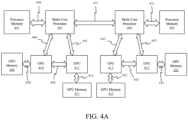
- the I/O hub 107 can enable a display controller, which may be included in the one or more processor(s) 102, to provide outputs to one or more display device(s) 110A.
- the one or more display device(s) 110A coupled with the I/O hub 107 can include a local, internal, or embedded display device.
- the one or more parallel processor(s) 112 incorporate circuitry optimized for graphics and video processing, including, for example, video output circuitry, and constitutes a graphics processing unit (GPU).
- the one or more parallel processor(s) 112 incorporate circuitry optimized for general purpose processing, while preserving the underlying computational architecture, described in greater detail herein.
- components of the computing system 100 may be integrated with one or more other system elements on a single integrated circuit.
- the one or more parallel processor(s), 112 memory hub 105, processor(s) 102, and I/O hub 107 can be integrated into a system on chip (SoC) integrated circuit.
- SoC system on chip
- the components of the computing system 100 can be integrated into a single package to form a system in package (SIP) configuration.
- SIP system in package
- at least a portion of the components of the computing system 100 can be integrated into a multi-chip module (MCM), which can be interconnected with other multi-chip modules into a modular computing system.
- MCM multi-chip module
- the host interface 206 can direct work operations to perform those commands to a front end 208.
- the front end 208 couples with a scheduler 210, which is configured to distribute commands or other work items to a processing cluster array 212.
- the scheduler 210 ensures that the processing cluster array 212 is properly configured and in a valid state before tasks are distributed to the processing clusters of the processing cluster array 212.
- Each of the one or more instances of the parallel processing unit 202 can couple with parallel processor memory 222.
- the parallel processor memory 222 can be accessed via the memory crossbar 216, which can receive memory requests from the processing cluster array 212 as well as the I/O unit 204.
- the memory crossbar 216 can access the parallel processor memory 222 via a memory interface 218.
- the memory interface 218 can include multiple partition units (e.g., partition unit 220A, partition unit 220B, through partition unit 220N) that can each couple to a portion (e.g., memory unit) of parallel processor memory 222.
- the number of partition units 220A-220N is configured to be equal to the number of memory units, such that a first partition unit 220A has a corresponding first memory unit 224A, a second partition unit 220B has a corresponding memory unit 224B, and an Nth partition unit 220N has a corresponding Nth memory unit 224N. In other embodiments, the number of partition units 220A-220N may not be equal to the number of memory devices.
- Operation of the processing cluster 214 can be controlled via a pipeline manager 232 that distributes processing tasks to SIMT parallel processors.
- the pipeline manager 232 receives instructions from the scheduler 210 of Figure 2 and manages execution of those instructions via a graphics multiprocessor 234 and/or a texture unit 236.
- the illustrated graphics multiprocessor 234 is an exemplary instance of an SIMT parallel processor. However, various types of SIMT parallel processors of differing architectures may be included within the processing cluster 214.
- One or more instances of the graphics multiprocessor 234 can be included within a processing cluster 214.
- the graphics multiprocessor 234 can process data and a data crossbar 240 can be used to distribute the processed data to one of multiple possible destinations, including other shader units.
- the pipeline manager 232 can facilitate the distribution of processed data by specifying destinations for processed data to be distributed vis the data crossbar 240.
- the graphics multiprocessor 234 includes an internal cache memory to perform load and store operations. In one embodiment, the graphics multiprocessor 234 can forego an internal cache and use a cache memory (e.g., L1 cache 308) within the processing cluster 214. Each graphics multiprocessor 234 also has access to L2 caches within the partition units (e.g., partition units 220A-220N of Figure 2 ) that are shared among all processing clusters 214 and may be used to transfer data between threads. The graphics multiprocessor 234 may also access off-chip global memory, which can include one or more of local parallel processor memory and/or system memory. Any memory external to the parallel processing unit 202 may be used as global memory. Embodiments in which the processing cluster 214 includes multiple instances of the graphics multiprocessor 234 can share common instructions and data, which may be stored in the L1 cache 308.
- L1 cache 308 e.g., L1 cache 308
- Each graphics multiprocessor 234 also has access to L2 caches within the partition units (e.g.,
- the instruction cache 252 receives a stream of instructions to execute from the pipeline manager 232.
- the instructions are cached in the instruction cache 252 and dispatched for execution by the instruction unit 254.
- the instruction unit 254 can dispatch instructions as thread groups (e.g., warps), with each thread of the thread group assigned to a different execution unit within GPGPU core 262.
- An instruction can access any of a local, shared, or global address space by specifying an address within a unified address space.
- the address mapping unit 256 can be used to translate addresses in the unified address space into a distinct memory address that can be accessed by the load/store units 266.
- the register file 258 provides a set of registers for the functional units of the graphics multiprocessor 324.
- the register file 258 provides temporary storage for operands connected to the data paths of the functional units (e.g., GPGPU cores 262, load/store units 266) of the graphics multiprocessor 324.
- the register file 258 is divided between each of the functional units such that each functional unit is allocated a dedicated portion of the register file 258.
- the register file 258 is divided between the different warps being executed by the graphics multiprocessor 324.
- the GPGPU cores 262 can each include floating point units (FPUs) and/or integer arithmetic logic units (ALUs) that are used to execute instructions of the graphics multiprocessor 324.
- the GPGPU cores 262 can be similar in architecture or can differ in architecture, according to embodiments.
- a first portion of the GPGPU cores 262 include a single precision FPU and an integer ALU while a second portion of the GPGPU cores include a double precision FPU.
- the FPUs can implement the IEEE 754-2008 standard for floating point arithmetic or enable variable precision floating point arithmetic.
- the graphics multiprocessor 324 can additionally include one or more fixed function or special function units to perform specific functions such as copy rectangle or pixel blending operations.
- one or more of the GPGPU cores can also include fixed or special function logic.
- the cache memory 272 can be used as a data cache for example, to cache texture data communicated between the functional units and the texture unit 236.
- the shared memory 270 can also be used as a program managed cached. Threads executing on the GPGPU cores 262 can programmatically store data within the shared memory in addition to the automatically cached data that is stored within the cache memory 272.
- Figure 3A shows a graphics multiprocessor 325 according to an additional embodiment.
- the graphics multiprocessor 325 includes multiple additional instances of execution resource units relative to the graphics multiprocessor 234 of Figure 2D .
- the graphics multiprocessor 325 can include multiple instances of the instruction unit 332A-332B, register file 334A-334B, and texture unit(s) 344A-344B.
- the graphics multiprocessor 325 also includes multiple sets of graphics or compute execution units (e.g., GPGPU core 336A-336B, GPGPU core 337A-337B, GPGPU core 338A-338B) and multiple sets of load/store units 340A-340B.
- FIG. 1 the architecture described in Figures 1 , 2A-2D , and 3A-3B are descriptive and not limiting as to the scope of the present embodiments.
- the techniques described herein may be implemented on any properly configured processing unit, including, without limitation, one or more mobile application processors, one or more desktop or server central processing units (CPUs) including multi-core CPUs, one or more parallel processing units, such as the parallel processing unit 202 of Figure 2 , as well as one or more graphics processors or special purpose processing units, without departure from the scope of the embodiments described herein.
- CPUs desktop or server central processing units
- parallel processing units such as the parallel processing unit 202 of Figure 2
- graphics processors or special purpose processing units without departure from the scope of the embodiments described herein.
- the illustrated processor 407 includes a plurality of cores 460A-460D, each with a translation lookaside buffer 461A-461D and one or more caches 462A-462D.
- the cores may include various other components for executing instructions and processing data which are not illustrated to avoid obscuring the underlying principles of the invention (e.g., instruction fetch units, branch prediction units, decoders, execution units, reorder buffers, etc.).
- the caches 462A-462D may comprise level 1 (L1) and level 2 (L2) caches.
- one or more shared caches 426 may be included in the caching hierarchy and shared by sets of the cores 460A-460D.
- a proxy circuit 425 communicatively couples the graphics acceleration module 446 to the coherence bus 464, allowing the graphics acceleration module 446 to participate in the cache coherence protocol as a peer of the cores.
- an interface 435 provides connectivity to the proxy circuit 425 over high-speed link 440 (e.g., a PCIe bus, NVLink, etc.) and an interface 437 connects the graphics acceleration module 446 to the link 440.
- high-speed link 440 e.g., a PCIe bus, NVLink, etc.
- the accelerator integration circuit 436 includes a memory management unit (MMU) 439 for performing various memory management functions such as virtual-to-physical memory translations (also referred to as effective-to-real memory translations) and memory access protocols for accessing system memory 441.
- the MMU 439 may also include a translation lookaside buffer (TLB) (not shown) for caching the virtual/effective to physical/real address translations.
- a cache 438 stores commands and data for efficient access by the graphics processing engines 431-432, N.
- the data stored in cache 438 and graphics memories 433-434, N is kept coherent with the core caches 462A-462D, 456 and system memory 411.
- proxy circuit 425 which takes part in the cache coherency mechanism on behalf of cache 438 and memories 433-434, N (e.g., sending updates to the cache 438 related to modifications/accesses of cache lines on processor caches 462A-462D, 456 and receiving updates from the cache 438).
- virtual/effective addresses from a graphics processing engine 431 are translated to real/physical addresses in system memory 411 by the MMU 439.
- One embodiment of the accelerator integration circuit 436 supports multiple (e.g., 4, 8, 16) graphics accelerator modules 446 and/or other accelerator devices.
- the graphics accelerator module 446 may be dedicated to a single application executed on the processor 407 or may be shared between multiple applications.
- a virtualized graphics execution environment is presented in which the resources of the graphics processing engines 431-432, N are shared with multiple applications or virtual machines (VMs).
- the resources may be subdivided into "slices" which are allocated to different VMs and/or applications based on the processing requirements and priorities associated with the VMs and/or applications.
- One function of the accelerator integration circuit 436 is the physical separation of the graphics processing engines 431-432, N so that they appear to the system as independent units.
- the system hypervisor 496 owns the graphics acceleration module 446 and makes its function available to all operating systems 495.
- the graphics acceleration module 446 may adhere to the following requirements: 1) An application's job request must be autonomous (that is, the state does not need to be maintained between jobs), or the graphics acceleration module 446 must provide a context save and restore mechanism. 2) An application's job request is guaranteed by the graphics acceleration module 446 to complete in a specified amount of time, including any translation faults, or the graphics acceleration module 446 provides the ability to preempt the processing of the job. 3) The graphics acceleration module 446 must be guaranteed fairness between processes when operating in the directed shared programming model.
- the AMR value is the AMR state to use for the current process.
- the value passed to the operating system is similar to an application setting the AMR. If the accelerator integration circuit 436 and graphics acceleration module 446 implementations do not support a User Authority Mask Override Register (UAMOR), the operating system may apply the current UAMOR value to the AMR value before passing the AMR in the hypervisor call.
- the hypervisor 496 may optionally apply the current Authority Mask Override Register (AMOR) value before placing the AMR into the process element 483.
- the CSRP is one of the registers 445 containing the effective address of an area in the application's address space 482 for the graphics acceleration module 446 to save and restore the context state. This pointer is optional if no state is required to be saved between jobs or when a job is preempted.
- the context save/restore area may be pinned system memory.
- the operating system 495 may verify that the application 480 has registered and been given the authority to use the graphics acceleration module 446. The operating system 495 then calls the hypervisor 496 with the information shown in Table 3. Table 3 - OS to Hypervisor Call Parameters 1 A work descriptor (WD) 2 An Authority Mask Register (AMR) value (potentially masked). 3 An effective address (EA) Context Save/Restore Area Pointer (CSRP) 4 A process ID (PID) and optional thread ID (TID) 5 A virtual address (VA) accelerator utilization record pointer (AURP) 6 The virtual address of the storage segment table pointer (SSTP) 7 A logical interrupt service number (LISN)
- the hypervisor 496 Upon receiving the hypervisor call, the hypervisor 496 verifies that the operating system 495 has registered and been given the authority to use the graphics acceleration module 446. The hypervisor 496 then puts the process element 483 into the process element linked list for the corresponding graphics acceleration module 446 type.
- the process element may include the information shown in Table 4.
- Table 4 - Process Element Information 1 A work descriptor (WD) 2 An Authority Mask Register (AMR) value (potentially masked).
- the hypervisor initializes a plurality of accelerator integration slice 490 registers 445.
- one embodiment of the invention employs a unified memory addressable via a common virtual memory address space used to access the physical processor memories 401-402 and GPU memories 420-423.
- operations executed on the GPUs 410-413 utilize the same virtual/effective memory address space to access the processors memories 401-402 and vice versa, thereby simplifying programmability.
- a first portion of the virtual/effective address space is allocated to the processor memory 401, a second portion to the second processor memory 402, a third portion to the GPU memory 420, and so on.
- the entire virtual/effective memory space (sometimes referred to as the effective address space) is thereby distributed across each of the processor memories 401-402 and GPU memories 420-423, allowing any processor or GPU to access any physical memory with a virtual address mapped to that memory.
- FIG. 5 illustrates a graphics processing pipeline 500, according to an embodiment.
- a graphics processor can implement the illustrated graphics processing pipeline 500.
- the graphics processor can be included within the parallel processing subsystems as described herein, such as the parallel processor 200 of Figure 2 , which, in one embodiment, is a variant of the parallel processor(s) 112 of Figure 1 .
- the various parallel processing systems can implement the graphics processing pipeline 500 via one or more instances of the parallel processing unit (e.g., parallel processing unit 202 of Figure 2 ) as described herein.
- term “user” may be interchangeably referred to as “viewer”, “observer”, “person”, “individual”, “end-user”, and/or the like. It is to be noted that throughout this document, terms like “graphics domain” may be referenced interchangeably with “graphics processing unit”, “graphics processor”, or simply “GPU” and similarly, “CPU domain” or “host domain” may be referenced interchangeably with “computer processing unit”, “application processor”, or simply “CPU”.
- Computing device 600 may include any number and type of communication devices, such as large computing systems, such as server computers, desktop computers, etc., and may further include set-top boxes (e.g., Internet-based cable television set-top boxes, etc.), global positioning system (GPS)-based devices, etc.
- Computing device 600 may include mobile computing devices serving as communication devices, such as cellular phones including smartphones, personal digital assistants (PDAs), tablet computers, laptop computers, e-readers, smart televisions, television platforms, wearable devices (e.g., glasses, watches, bracelets, smartcards, jewelry, clothing items, etc.), media players, etc.
- a graphics pipeline may be implemented in a graphics coprocessor design, where CPU 612 is designed to work with GPU 614 which may be included in or co-located with CPU 612.
- GPU 614 may employ any number and type of conventional software and hardware logic to perform the conventional functions relating to graphics rendering as well as novel software and hardware logic to execute any number and type of instructions.
- I/O sources 604 may include one or more I/O devices that are implemented for transferring data to and/or from computing device 600 (e.g., a networking adapter); or, for a large scale non-volatile storage within computing device 600 (e.g., hard disk drive).
- User input device including alphanumeric and other keys, may be used to communicate information and command selections to GPU 614.
- cursor control such as a mouse, a trackball, a touchscreen, a touchpad, or cursor direction keys to communicate direction information and command selections to GPU 614 and to control cursor movement on the display device.
- Camera and microphone arrays of computer device 600 may be employed to observe gestures, record audio and video and to receive and transmit visual and audio commands.
- Network interface(s) may include one or more communication interfaces, such as a modem, a network interface card, or other well-known interface devices, such as those used for coupling to the Ethernet, token ring, or other types of physical wired or wireless attachments for purposes of providing a communication link to support a LAN or a WAN, for example.
- the computer system may also be coupled to a number of peripheral devices, clients, control surfaces, consoles, or servers via a conventional network infrastructure, including an Intranet or the Internet, for example.
- a machine-readable medium may include, but is not limited to, floppy diskettes, optical disks, CD-ROMs (Compact Disc-Read Only Memories), and magneto-optical disks, ROMs, RAMs, EPROMs (Erasable Programmable Read Only Memories), EEPROMs (Electrically Erasable Programmable Read Only Memories), magnetic or optical cards, flash memory, or other type of media/machine-readable medium suitable for storing machine-executable instructions.
- embodiments may be downloaded as a computer program product, wherein the program may be transferred from a remote computer (e.g., a server) to a requesting computer (e.g., a client) by way of one or more data signals embodied in and/or modulated by a carrier wave or other propagation medium via a communication link (e.g., a modem and/or network connection).
- a remote computer e.g., a server
- a requesting computer e.g., a client
- a communication link e.g., a modem and/or network connection
- logic 730 includes a FP16 processing component and a delta processing component. Whenever a 32-bit operation is received, FP16 is implemented to process the lower 16-bits, while the delta component is used to process the upper 16-bits. In a further embodiment, 16-bit operations are also processed at logic 730. However in this embodiment, 16-bit operations are processed by only the FP16 operations received at logic 730. In yet a further embodiment, compute mechanism 610 may shut down power to the delta component during processing of 16-bit operations, thus saving power. In other embodiments, compute mechanism 610 may process operations having higher bit depths (e.g., 64-bit).
- An exemplary type of machine learning algorithm is a neural network.
- a simple type of neural network is a feedforward network.
- a feedforward network may be implemented as an acyclic graph in which the nodes are arranged in layers.
- a feedforward network topology includes an input layer and an output layer that are separated by at least one hidden layer.
- the hidden layer transforms input received by the input layer into a representation that is useful for generating output in the output layer.
- the network nodes are fully connected via edges to the nodes in adjacent layers, but there are no edges between nodes within each layer.
- Data received at the nodes of an input layer of a feedforward network are propagated (i.e., "fed forward") to the nodes of the output layer via an activation function that calculates the states of the nodes of each successive layer in the network based on coefficients ("weights") respectively associated with each of the edges connecting the layers.
- the output from the neural network algorithm can take various forms.
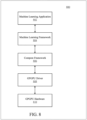
- Figure 8 is a generalized diagram of a machine learning software stack 800.
- a machine learning application 802 can be configured to train a neural network using a training dataset or to use a trained deep neural network to implement machine intelligence.
- the machine learning application 802 can include training and inference functionality for a neural network and/or specialized software that can be used to train a neural network before deployment.
- the machine learning application 802 can implement any type of machine intelligence including but not limited to image recognition, mapping and localization, autonomous navigation, speech synthesis, medical imaging, or language translation.
- Hardware acceleration for the machine learning application 802 can be enabled via a machine learning framework 804.
- the machine learning framework 804 can provide a library of machine learning primitives.
- Machine learning primitives are basic operations that are commonly performed by machine learning algorithms. Without the machine learning framework 804, developers of machine learning algorithms would be required to create and optimize the main computational logic associated with the machine learning algorithm, then re-optimize the computational logic as new parallel processors are developed. Instead, the machine learning application can be configured to perform the necessary computations using the primitives provided by the machine learning framework 804.
- Exemplary primitives include tensor convolutions, activation functions, and pooling, which are computational operations that are performed while training a convolutional neural network (CNN).
- CNN convolutional neural network
- the machine learning framework 804 can also provide primitives to implement basic linear algebra subprograms performed by many machine-learning algorithms, such as matrix and vector operations.
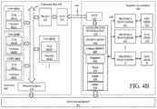
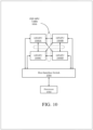
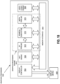
- the GPGPU 900 includes a host interface 902 to enable a connection with a host processor.
- the host interface 902 is a PCI Express interface.
- the host interface can also be a vendor specific communications interface or communications fabric.
- the GPGPU 900 receives commands from the host processor and uses a global scheduler 904 to distribute execution threads associated with those commands to a set of compute clusters 906AH.
- the compute clusters 906A-H share a cache memory 908.
- the cache memory 908 can serve as a higher-level cache for cache memories within the compute clusters 906A-H.
- each compute cluster GPLAB06A-H includes a set of graphics multiprocessors, such as the graphics multiprocessor 400 of Figure 4A .
- the graphics multiprocessors of the compute cluster multiple types of integer and floating point logic units that can perform computational operations at a range of precisions including suited for machine learning computations.
- at least a subset of the floating point units in each of the compute clusters 906A-H can be configured to perform 16-bit or 32-bit floating point operations, while a different subset of the floating point units can be configured to perform 64-bit floating point operations.
- Multiple instances of the GPGPU 900 can be configured to operate as a compute cluster.
- the communication mechanism used by the compute cluster for synchronization and data exchange varies across embodiments.
- the multiple instances of the GPGPU 900 communicate over the host interface 902.
- the GPGPU 900 includes an I/O hub 908 that couples the GPGPU 900 with a GPU link 910 that enables a direct connection to other instances of the GPGPU.
- the GPU link 910 is coupled to a dedicated GPU-to-GPU bridge that enables communication and synchronization between multiple instances of the GPGPU 900.
- the GPU link 910 couples with a high speed interconnect to transmit and receive data to other GPGPUs or parallel processors.
- the multiple instances of the GPGPU 900 are located in separate data processing systems and communicate via a network device that is accessible via the host interface 902.
- the GPU link 910 can be configured to enable a connection to a host processor in addition to or as an alternative to the host interface 902.
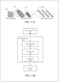
- FIG 10 illustrates a multi-GPU computing system 1000, according to an embodiment.
- the multi-GPU computing system 1000 can include a processor 1002 coupled to multiple GPGPUs 1006A-D via a host interface switch 1004.
- the host interface switch 1004 in one embodiment, is a PCI express switch device that couples the processor 1002 to a PCI express bus over which the processor 1002 can communicate with the set of GPGPUs 1006A-D.
- Each of the multiple GPGPUs 1006A-D can be an instance of the GPGPU 900 of Figure 9 .
- the GPGPUs 1006A-D can interconnect via a set of high-speed point to point GPU to GPU links 1016.
- the high-speed GPU to GPU links can connect to each of the GPGPUs 1006A-D via a dedicated GPU link, such as the GPU link 910 as in Figure 9 .
- the P2P GPU links 1016 enable direct communication between each of the GPGPUs 1006A-D without requiring communication over the host interface bus to which the processor 1002 is connected. With GPU-to-GPU traffic directed to the P2P GPU links, the host interface bus remains available for system memory access or to communicate with other instances of the multi-GPU computing system 1000, for example, via one or more network devices. While in the illustrated embodiment the GPGPUs 1006A-D connect to the processor 1002 via the host interface switch 1004, in one embodiment the processor 1002 includes direct support for the P2P GPU links 1016 and can connect directly to the GPGPUs 1006A-D.
- a second exemplary type of neural network is the Convolutional Neural Network (CNN).
- CNN is a specialized feedforward neural network for processing data having a known, grid-like topology, such as image data. Accordingly, CNNs are commonly used for compute vision and image recognition applications, but they also may be used for other types of pattern recognition such as speech and language processing.
- the nodes in the CNN input layer are organized into a set of "filters" (feature detectors inspired by the receptive fields found in the retina), and the output of each set of filters is propagated to nodes in successive layers of the network.
- the computations for a CNN include applying the convolution mathematical operation to each filter to produce the output of that filter.
- a learning model can be applied to the network to train the network to perform specific tasks.
- the learning model describes how to adjust the weights within the model to reduce the output error of the network.
- Backpropagation of errors is a common method used to train neural networks. An input vector is presented to the network for processing. The output of the network is compared to the desired output using a loss function and an error value is calculated for each of the neurons in the output layer. The error values are then propagated backwards until each neuron has an associated error value which roughly represents its contribution to the original output. The network can then learn from those errors using an algorithm, such as the stochastic gradient descent algorithm, to update the weights of the of the neural network.
- an algorithm such as the stochastic gradient descent algorithm
- the convolutional layers are sparsely connected, which differs from traditional neural network configuration found in the fully connected layers 1108.
- Traditional neural network layers are fully connected, such that every output unit interacts with every input unit.
- the convolutional layers are sparsely connected because the output of the convolution of a field is input (instead of the respective state value of each of the nodes in the field) to the nodes of the subsequent layer, as illustrated.
- the kernels associated with the convolutional layers perform convolution operations, the output of which is sent to the next layer.
- the dimensionality reduction performed within the convolutional layers is one aspect that enables the CNN to scale to process large images.
- Unsupervised learning is a learning method in which the network attempts to train itself using unlabeled data.
- the training dataset 1302 will include input data without any associated output data.
- the untrained neural network 1306 can learn groupings within the unlabeled input and can determine how individual inputs are related to the overall dataset.
- Unsupervised training can be used to generate a self-organizing map, which is a type of trained neural network 1307 capable of performing operations useful in reducing the dimensionality of data.
- Unsupervised training can also be used to perform anomaly detection, which allows the identification of data points in an input dataset that deviate from the normal patterns of the data.
- model parallelism 1402 different computational nodes in a distributed system can perform training computations for different parts of a single network. For example, each layer of a neural network can be trained by a different processing node of the distributed system.
- the benefits of model parallelism include the ability to scale to particularly large models. Splitting the computations associated with different layers of the neural network enables the training of very large neural networks in which the weights of all layers would not fit into the memory of a single computational node. In some instances, model parallelism can be particularly useful in performing unsupervised training of large neural networks.
- data parallelism 1404 the different nodes of the distributed network have a complete instance of the model and each node receives a different portion of the data. The results from the different nodes are then combined. While different approaches to data parallelism are possible, data parallel training approaches all require a technique of combining results and synchronizing the model parameters between each node. Exemplary approaches to combining data include parameter averaging and update based data parallelism. Parameter averaging trains each node on a subset of the training data and sets the global parameters (e.g., weights, biases) to the average of the parameters from each node. Parameter averaging uses a central parameter server that maintains the parameter data.
- parameter averaging trains each node on a subset of the training data and sets the global parameters (e.g., weights, biases) to the average of the parameters from each node. Parameter averaging uses a central parameter server that maintains the parameter data.
- Combined model and data parallelism 1406 can be implemented, for example, in a distributed system in which each computational node includes multiple GPUs. Each node can have a complete instance of the model with separate GPUs within each node are used to train different portions of the model.
- ASR automatic speech recognition
- HMMs hidden Markov models
- GMMs Gaussian mixture models
- Parallel processor accelerated machine learning can also be used to accelerate natural language processing.
- Automatic learning procedures can make use of statistical inference algorithms to produce models that are robust to erroneous or unfamiliar input.
- Exemplary natural language processor applications include automatic machine translation between human languages.
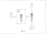
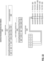
- FIG. 15 illustrates an exemplary inferencing system on a chip (SOC) 1500 suitable for performing inferencing using a trained model.
- the SOC 1500 can integrate processing components including a media processor 1502, a vision processor 1504, a GPGPU 1506 and a multi-core processor 1508.
- the SOC 1500 can additionally include on-chip memory 1505 that can enable a shared on-chip data pool that is accessible by each of the processing components.
- the processing components can be optimized for low power operation to enable deployment to a variety of machine learning platforms, including autonomous vehicles and autonomous robots.
- one implementation of the SOC 1500 can be used as a portion of the main control system for an autonomous vehicle. Where the SOC 1500 is configured for use in autonomous vehicles the SOC is designed and configured for compliance with the relevant functional safety standards of the deployment jurisdiction.
- the multi-core processor 1508 can include control logic to assist with sequencing and synchronization of data transfers and shared memory operations performed by the media processor 1502 and the vision processor 1504.
- the multi-core processor 1308 can also function as an application processor to execute software applications that can make use of the inferencing compute capability of the GPGPU 1506. For example, at least a portion of the navigation and driving logic can be implemented in software executing on the multi-core processor 1508. Such software can directly issue computational workloads to the GPGPU 1506 or the computational workloads can be issued to the multi-core processor 1508, which can offload at least a portion of those operations to the GPGPU 1506.
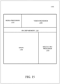
- Figure 16 is a block diagram of a processing system 1600, according to an embodiment.
- the system 1600 includes one or more processors 1602 and one or more graphics processors 1608, and may be a single processor desktop system, a multiprocessor workstation system, or a server system having a large number of processors 1602 or processor cores 1607.
- the system 1600 is a processing platform incorporated within a system-on-a-chip (SoC) integrated circuit for use in mobile, handheld, or embedded devices.
- SoC system-on-a-chip
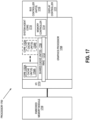
- FIG 17 is a block diagram of an embodiment of a processor 1700 having one or more processor cores 1702A-1702N, an integrated memory controller 1714, and an integrated graphics processor 1708. Those elements of Figure 17 having the same reference numbers (or names) as the elements of any other figure herein can operate or function in any manner similar to that described elsewhere herein, but are not limited to such.
- Processor 1700 can include additional cores up to and including additional core 1702N represented by the dashed lined boxes.
- Each of processor cores 1702A-1702N includes one or more internal cache units 1704A-1704N. In some embodiments each processor core also has access to one or more shared cached units 1706.
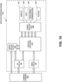
- FIG 18 is a block diagram of a graphics processor 1800, which may be a discrete graphics processing unit, or may be a graphics processor integrated with a plurality of processing cores.
- the graphics processor communicates via a memory mapped I/O interface to registers on the graphics processor and with commands placed into the processor memory.
- graphics processor 1800 includes a memory interface 1814 to access memory.
- Memory interface 1814 can be an interface to local memory, one or more internal caches, one or more shared external caches, and/or to system memory.
- GPE 1910 couples with or includes a command streamer 1903, which provides a command stream to the 3D pipeline 1812 and/or media pipelines 1816.
- command streamer 1903 is coupled with memory, which can be system memory, or one or more of internal cache memory and shared cache memory.
- command streamer 1903 receives commands from the memory and sends the commands to 3D pipeline 1812 and/or media pipeline 1816.
- the commands are directives fetched from a ring buffer, which stores commands for the 3D pipeline 1812 and media pipeline 1816.
- the ring buffer can additionally include batch command buffers storing batches of multiple commands.
- Output data generated by threads executing on the graphics core array 1914 can output data to memory in a unified return buffer (URB) 1918.
- the URB 1918 can store data for multiple threads.
- the URB 1918 may be used to send data between different threads executing on the graphics core array 1914.
- the URB 1918 may additionally be used for synchronization between threads on the graphics core array and fixed function logic within the shared function logic 1920.
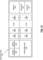
- thread execution logic 2100 includes a shader processor 2102, a thread dispatcher 2104, instruction cache 2106, a scalable execution unit array including a plurality of execution units 2108A-2108N, a sampler 2110, a data cache 2112, and a data port 2114.
- the scalable execution unit array can dynamically scale by enabling or disabling one or more execution units (e.g., any of execution unit 2108A, 2108B, 2108C, 2108D, through 2108N-1 and 2108N) based on the computational requirements of a workload.
- the included components are interconnected via an interconnect fabric that links to each of the components.
- thread execution logic 2100 includes one or more connections to memory, such as system memory or cache memory, through one or more of instruction cache 2106, data port 2114, sampler 2110, and execution units 2108A-2108N.
- each execution unit e.g. 2108A
- the array of execution units 2108A-2108N is scalable to include any number individual execution units.
- pixel processor logic within the shader processor 2102 then executes an application programming interface (API)-supplied pixel or fragment shader program.
- API application programming interface
- the shader processor 2102 dispatches threads to an execution unit (e.g., 2108A) via thread dispatcher 2104.
- pixel shader 2102 uses texture sampling logic in the sampler 2110 to access texture data in texture maps stored in memory. Arithmetic operations on the texture data and the input geometry data compute pixel color data for each geometric fragment, or discards one or more pixels from further processing.
- the address mode portion of the access/address mode field 2226 determines whether the instruction is to use direct or indirect addressing.
- direct register addressing mode bits in the instruction directly provide the register address of one or more operands.
- indirect register addressing mode the register address of one or more operands may be computed based on an address register value and an address immediate field in the instruction.
- instructions are grouped based on opcode 2212 bit-fields to simplify Opcode decode 2240.
- bits 4, 5, and 6 allow the execution unit to determine the type of opcode.
- the precise opcode grouping shown is merely an example.
- a move and logic opcode group 2242 includes data movement and logic instructions (e.g., move (mov), compare (cmp)).
- move and logic group 2242 shares the five most significant bits (MSB), where move (mov) instructions are in the form of 0000xxxxb and logic instructions are in the form of 0001xxxxb.
- a flow control instruction group 2244 (e.g., call, jump (jmp)) includes instructions in the form of 0010xxxxb (e.g., 0x20).
- a miscellaneous instruction group 2246 includes a mix of instructions, including synchronization instructions (e.g., wait, send) in the form of 001 1xxxxb (e.g., 0x30).
- a parallel math instruction group 2248 includes component-wise arithmetic instructions (e.g., add, multiply (mul)) in the form of 0100xxxxb (e.g., 0x40). The parallel math group 2248 performs the arithmetic operations in parallel across data channels.
- the vector math group 2250 includes arithmetic instructions (e.g., dp4) in the form of 0101xxxxb (e.g., 0x50).
- the vector math group performs arithmetic such as dot product calculations on vector operands.
- graphics pipeline 2320 includes tessellation components to perform hardware-accelerated tessellation of 3D objects.
- a programmable hull shader 811 configures the tessellation operations.
- a programmable domain shader 817 provides back-end evaluation of tessellation output.
- a tessellator 2313 operates at the direction of hull shader 2311 and contains special purpose logic to generate a set of detailed geometric objects based on a coarse geometric model that is provided as input to graphics pipeline 2320.
- tessellation components e.g., hull shader 2311, tessellator 2313, and domain shader 2317
- the graphics processor 2300 has an interconnect bus, interconnect fabric, or some other interconnect mechanism that allows data and message passing amongst the major components of the processor.
- execution units 2352A-2352B and associated cache(s) 2351, texture and media sampler 2354, and texture/sampler cache 2358 interconnect via a data port 2356 to perform memory access and communicate with render output pipeline components of the processor.
- sampler 2354, caches 2351, 2358 and execution units 2352A-2352B each have separate memory access paths.
- graphics processor media pipeline 2330 includes a media engine 2337 and a video front end 2334.
- video front end 2334 receives pipeline commands from the command streamer 2303.
- media pipeline 2330 includes a separate command streamer.
- video front-end 2334 processes media commands before sending the command to the media engine 2337.
- media engine 2337 includes thread spawning functionality to spawn threads for dispatch to thread execution logic 2350 via thread dispatcher 2331.
- return buffer state commands 2416 are used to configure a set of return buffers for the respective pipelines to write data. Some pipeline operations require the allocation, selection, or configuration of one or more return buffers into which the operations write intermediate data during processing. In some embodiments, the graphics processor also uses one or more return buffers to store output data and to perform cross thread communication. In some embodiments, the return buffer state 2416 includes selecting the size and number of return buffers to use for a set of pipeline operations.
- the remaining commands in the command sequence differ based on the active pipeline for operations. Based on a pipeline determination 2420, the command sequence is tailored to the 3D pipeline 2422 beginning with the 3D pipeline state 2430 or the media pipeline 2424 beginning at the media pipeline state 2440.
- 3D pipeline 2422 is triggered via an execute 2434 command or event.
- a register write triggers command execution.
- execution is triggered via a 'go' or 'kick' command in the command sequence.
- command execution is triggered using a pipeline synchronization command to flush the command sequence through the graphics pipeline.
- the 3D pipeline will perform geometry processing for the 3D primitives. Once operations are complete, the resulting geometric objects are rasterized and the pixel engine colors the resulting pixels. Additional commands to control pixel shading and pixel back end operations may also be included for those operations.
- FIG. 27 is a block diagram illustrating an exemplary system on a chip integrated circuit 2700 that may be fabricated using one or more IP cores, according to an embodiment.
- Exemplary integrated circuit 2700 includes one or more application processor(s) 2705 (e.g., CPUs), at least one graphics processor 2710, and may additionally include an image processor 2715 and/or a video processor 2720, any of which may be a modular IP core from the same or multiple different design facilities.
- Integrated circuit 2700 includes peripheral or bus logic including a USB controller 2725, UART controller 2730, an SPI/SDIO controller 2735, and an I 2 S/I 2 C controller 2740.
- Figure 28 is a block diagram illustrating an exemplary graphics processor 2810 of a system on a chip integrated circuit that may be fabricated using one or more IP cores, according to an embodiment.
- Graphics processor 2810 can be a variant of the graphics processor 2710 of Figure 27 .
- Graphics processor 2810 includes a vertex processor 2805 and one or more fragment processor(s) 2815A-2815N (e.g., 2815A, 2815B, 2815C, 2815D, through 2815N-1, and 2815N).
- the one or more MMU(s) 2825A-2825B may be synchronized with other MMUs within the system, including one or more MMUs associated with the one or more application processor(s) 2705, image processor 2715, and/or video processor 2720 of Figure 27 , such that each processor 2705-2720 can participate in a shared or unified virtual memory system.
- the one or more circuit interconnect(s) 2830A-2830B enable graphics processor 2810 to interface with other IP cores within the SoC, either via an internal bus of the SoC or via a direct connection, according to embodiments.
- Figure 29 is a block diagram illustrating an additional exemplary graphics processor 2910 of a system on a chip integrated circuit that may be fabricated using one or more IP cores, according to an embodiment.
- Graphics processor 2910 can be a variant of the graphics processor 2710 of Figure 27 .
- Graphics processor 2910 includes the one or more MMU(s) 2820A-2820B, caches 2825A-2825B, and circuit interconnects 2830A-2830B of the integrated circuit 2800 of Figure 28 .
- Graphics processor 2910 includes one or more shader core(s) 2915A-2915N (e.g., 2915A, 2915B, 2915C, 2915D, 2915E, 2915F, through 2915N-1, and 2915N), which provides for a unified shader core architecture in which a single core or type or core can execute all types of programmable shader code, including shader program code to implement vertex shaders, fragment shaders, and/or compute shaders. The exact number of shader cores present can vary among embodiments and implementations.
- Example 3 includes the subject matter of Examples 1 and 2, wherein the plurality of bins comprise a first bin to store floating point thread operations having a first bit depth and a second bin to store floating point thread operations having a second bit depth.
- Example 5 includes the subject matter of Examples 1-4, wherein the graphics processor further comprises floating logic to process threads into floating point thread operations having a higher bit depth.
- Example 8 includes the subject matter of Examples 1-7, wherein the floating point logic deactivates the second component during processing of the floating point thread operations having the lower bit depth at the first component.
- Example 12 includes the subject matter of Examples 1-11, further comprising a processing unit to receive the instruction, parse the instruction, convert all operands to the destination format and execute the operation.
- Example 13 includes a method to facilitate compute optimization at a processing unit, comprising receiving a plurality of processing threads and sorting the plurality of processing threads into thread groups based on bit depth of floating point thread operations.
- Example 16 includes the subject matter of Examples 13-15, further comprising processing the floating point thread operations.
- Example 19 includes the subject matter of Examples 13-18, wherein providing the variable precision support in a math instruction comprises receiving an instruction including an attribute to specify a format of each operand in an operation and a format of a final result, wherein one or more of the operands includes a different format.
Landscapes
- Engineering & Computer Science (AREA)
- Theoretical Computer Science (AREA)
- Physics & Mathematics (AREA)
- Software Systems (AREA)
- General Physics & Mathematics (AREA)
- General Engineering & Computer Science (AREA)
- Health & Medical Sciences (AREA)
- Life Sciences & Earth Sciences (AREA)
- Biomedical Technology (AREA)
- Biophysics (AREA)
- Computational Linguistics (AREA)
- Molecular Biology (AREA)
- Computing Systems (AREA)
- General Health & Medical Sciences (AREA)
- Evolutionary Computation (AREA)
- Mathematical Physics (AREA)
- Data Mining & Analysis (AREA)
- Artificial Intelligence (AREA)
- Computer Graphics (AREA)
- Computational Mathematics (AREA)
- Mathematical Analysis (AREA)
- Mathematical Optimization (AREA)
- Pure & Applied Mathematics (AREA)
- Neurology (AREA)
- Human Computer Interaction (AREA)
- Computer Hardware Design (AREA)
- Multimedia (AREA)
- Image Processing (AREA)
- Image Generation (AREA)
- Memory System Of A Hierarchy Structure (AREA)
Claims (12)
- Einrichtung zum Vereinfachen einer Rechenoptimierung, die einen Grafikprozessor (234, 350, 2000, 2300), der eine Sortierlogik (710) zum Sortieren von Gleitkomma-Verarbeitungsthreads in Threadgruppen basierend auf einer Bittiefe von Gleitkomma-Threadoperationen, und eine Gleitkommalogik (730) umfasst, wobei die Gleitkommalogik (730) umfasst:eine erste Komponente zum Verarbeiten einer unteren Hälfte einer ersten Bittiefe der Gleitkomma-Threadoperationen; undeine zweite Komponente zum Verarbeiten einer oberen Hälfte der ersten Bittiefe der Gleitkomma-Threadoperationen;wobei, wenn die Gleitkomma-Threadoperationen, die eine zweite Bittiefe aufweisen, die einer Hälfte der ersten Bittiefe entspricht, in der ersten Komponente verarbeitet werden, die Gleitkommalogik (730) die zweite Komponente deaktiviert.
- Einrichtung nach Anspruch 1, wobei die Sortierlogik (710) ferner eine Vielzahl von Bins (712, 714) zum Speichern der Threadgruppen umfasst, wobei jedes aus der Vielzahl von Bins (712, 714) mit einer Bittiefe assoziiert ist.
- Einrichtung nach Anspruch 2, wobei die Vielzahl von Bins (712, 714) umfasst:ein erstes Bin (712) zum Speichern von Gleitkomma-Threadoperationen, die eine erste Bittiefe aufweisen; undein zweites Bin (714) zum Speichern von Gleitkomma-Threadoperationen, die eine zweite Bittiefe aufweisen.
- Einrichtung nach Anspruch 3, wobei die erste Komponente und die zweite Komponente Gleitkommaeinheiten sind.
- Einrichtung nach Anspruch 1, wobei die erste Komponente und die zweite Komponente 16 -Bit-Gleitkommaeinheiten zum Verarbeiten von 32 -Bit-Threadoperationen sind.
- Einrichtung nach Anspruch 1, wobei der Grafikprozessor (234, 350, 2000, 2300) ferner eine Logik umfasst, um eine variable Genauigkeitsunterstützung in einer mathematischen Anweisung bereitzustellen.
- Einrichtung nach Anspruch 6, wobei die Logik eine Anweisung erzeugt, die ein Attribut beinhaltet, um ein Format von jedem Operanden in einer Operation und ein Format eines endgültigen Ergebnisses festzulegen.
- Einrichtung nach Anspruch 7, wobei einer oder mehrere der Operanden ein unterschiedliches Format umfassen.
- Einrichtung nach Anspruch 8, die ferner eine Verarbeitungseinheit (202) zum Empfangen der Anweisung, zum Analysieren der Anweisung, zum Umwandeln aller Operanden in das Zielformat und zum Ausführen der Operation umfasst.
- Verfahren zum Vereinfachen einer Rechenoptimierung in einer Verarbeitungseinheit (202), die eine Sortierlogik (710) und eine Gleitkommalogik (730) beinhaltet, die eine erste Komponente und eine zweite Komponente umfasst, wobei das Verfahren umfasst:Empfangen einer Vielzahl von Verarbeitungsthreads;Sortieren der Vielzahl von Verarbeitungsthreads in Threadgruppen basierend auf einer Bittiefe der Gleitkomma-Threadoperationen;Verarbeiten einer unteren Hälfte einer ersten Bittiefe der Gleitkomma-Threadoperationen in der ersten Komponente; undVerarbeiten einer oberen Hälfte der ersten Bittiefe der Gleitkomma-Threadoperationen in der zweiten Komponente; undfür Gleitkomma-Threadoperationen, die eine zweite Bittiefe aufweisen, die einer Hälfte der ersten Bittiefe entspricht:
Deaktivieren der zweiten Komponente. - Verfahren nach Anspruch 10, wobei jedes aus einer Vielzahl von Bins (712, 714) zum Speichern der Threadgruppen mit einer Bittiefe assoziiert ist.
- Verfahren nach Anspruch 11, wobei das Sortieren der Vielzahl von Verarbeitungsthreads umfasst: Sortieren von Gleitkomma-Threadoperationen, die eine erste Bittiefe aufweisen, in ein erstes Bin (712); und
Sortieren von Gleitkomma-Threadoperationen, die eine zweite Bittiefe aufweisen, in ein zweites Bin (714).
Priority Applications (4)
| Application Number | Priority Date | Filing Date | Title |
|---|---|---|---|
| EP19175038.9A EP3564813A1 (de) | 2017-04-24 | 2018-03-02 | Rechenoptimierungsmechanismus |
| EP19218464.6A EP3657323B1 (de) | 2017-04-24 | 2018-03-02 | Rechenoptimierungsmechanismus |
| EP19183024.9A EP3579103B1 (de) | 2017-04-24 | 2018-03-02 | Rechenoptimierungsmechanismus |
| EP20205015.9A EP3792839A1 (de) | 2017-04-24 | 2018-03-02 | Rechenoptimierungsmechanismus |
Applications Claiming Priority (1)
| Application Number | Priority Date | Filing Date | Title |
|---|---|---|---|
| US15/494,905 US10489877B2 (en) | 2017-04-24 | 2017-04-24 | Compute optimization mechanism |
Related Child Applications (8)
| Application Number | Title | Priority Date | Filing Date |
|---|---|---|---|
| EP20205015.9A Division EP3792839A1 (de) | 2017-04-24 | 2018-03-02 | Rechenoptimierungsmechanismus |
| EP20205015.9A Division-Into EP3792839A1 (de) | 2017-04-24 | 2018-03-02 | Rechenoptimierungsmechanismus |
| EP19175038.9A Division-Into EP3564813A1 (de) | 2017-04-24 | 2018-03-02 | Rechenoptimierungsmechanismus |
| EP19175038.9A Division EP3564813A1 (de) | 2017-04-24 | 2018-03-02 | Rechenoptimierungsmechanismus |
| EP19218464.6A Division EP3657323B1 (de) | 2017-04-24 | 2018-03-02 | Rechenoptimierungsmechanismus |
| EP19218464.6A Division-Into EP3657323B1 (de) | 2017-04-24 | 2018-03-02 | Rechenoptimierungsmechanismus |
| EP19183024.9A Division-Into EP3579103B1 (de) | 2017-04-24 | 2018-03-02 | Rechenoptimierungsmechanismus |
| EP19183024.9A Division EP3579103B1 (de) | 2017-04-24 | 2018-03-02 | Rechenoptimierungsmechanismus |
Publications (2)
| Publication Number | Publication Date |
|---|---|
| EP3396529A1 EP3396529A1 (de) | 2018-10-31 |
| EP3396529B1 true EP3396529B1 (de) | 2025-04-09 |
Family
ID=63638520
Family Applications (5)
| Application Number | Title | Priority Date | Filing Date |
|---|---|---|---|
| EP19175038.9A Ceased EP3564813A1 (de) | 2017-04-24 | 2018-03-02 | Rechenoptimierungsmechanismus |
| EP18159839.2A Active EP3396529B1 (de) | 2017-04-24 | 2018-03-02 | Rechenoptimierungsmechanismus |
| EP20205015.9A Pending EP3792839A1 (de) | 2017-04-24 | 2018-03-02 | Rechenoptimierungsmechanismus |
| EP19218464.6A Active EP3657323B1 (de) | 2017-04-24 | 2018-03-02 | Rechenoptimierungsmechanismus |
| EP19183024.9A Active EP3579103B1 (de) | 2017-04-24 | 2018-03-02 | Rechenoptimierungsmechanismus |
Family Applications Before (1)
| Application Number | Title | Priority Date | Filing Date |
|---|---|---|---|
| EP19175038.9A Ceased EP3564813A1 (de) | 2017-04-24 | 2018-03-02 | Rechenoptimierungsmechanismus |
Family Applications After (3)
| Application Number | Title | Priority Date | Filing Date |
|---|---|---|---|
| EP20205015.9A Pending EP3792839A1 (de) | 2017-04-24 | 2018-03-02 | Rechenoptimierungsmechanismus |
| EP19218464.6A Active EP3657323B1 (de) | 2017-04-24 | 2018-03-02 | Rechenoptimierungsmechanismus |
| EP19183024.9A Active EP3579103B1 (de) | 2017-04-24 | 2018-03-02 | Rechenoptimierungsmechanismus |
Country Status (6)
| Country | Link |
|---|---|
| US (7) | US10489877B2 (de) |
| EP (5) | EP3564813A1 (de) |
| CN (8) | CN116894762A (de) |
| ES (3) | ES3034021T3 (de) |
| PL (2) | PL3657323T3 (de) |
| TW (2) | TWI673678B (de) |
Families Citing this family (42)
| Publication number | Priority date | Publication date | Assignee | Title |
|---|---|---|---|---|
| US10489877B2 (en) | 2017-04-24 | 2019-11-26 | Intel Corporation | Compute optimization mechanism |
| US11373088B2 (en) * | 2017-12-30 | 2022-06-28 | Intel Corporation | Machine learning accelerator mechanism |
| US11216732B2 (en) * | 2018-05-31 | 2022-01-04 | Neuralmagic Inc. | Systems and methods for generation of sparse code for convolutional neural networks |
| US10636484B2 (en) * | 2018-09-12 | 2020-04-28 | Winbond Electronics Corporation | Circuit and method for memory operation |
| US10785786B2 (en) | 2018-09-26 | 2020-09-22 | Micron Technology, Inc. | Remotely executable instructions |
| US11922314B1 (en) * | 2018-11-30 | 2024-03-05 | Ansys, Inc. | Systems and methods for building dynamic reduced order physical models |
| CN109828732B (zh) * | 2018-12-26 | 2022-07-01 | 维沃移动通信有限公司 | 一种显示控制方法及终端设备 |
| US11520331B2 (en) * | 2018-12-28 | 2022-12-06 | Intel Corporation | Methods and apparatus to update autonomous vehicle perspectives |
| US11353870B2 (en) * | 2018-12-31 | 2022-06-07 | Baidu Usa Llc | Autonomous driving computing and storage expansion device with flexible host and client configuration |
| CN109829863B (zh) * | 2019-01-22 | 2021-06-25 | 深圳市商汤科技有限公司 | 图像处理方法及装置、电子设备和存储介质 |
| TWI734072B (zh) * | 2019-01-25 | 2021-07-21 | 鴻齡科技股份有限公司 | Gpu加速優化方法、裝置及電腦存儲介質 |
| TWI670721B (zh) * | 2019-02-13 | 2019-09-01 | 睿寬智能科技有限公司 | 用於儲存裝置之不正常斷電測試方法及設備 |
| CN113424148A (zh) | 2019-03-15 | 2021-09-21 | 英特尔公司 | 用于检测跨分片访问、提供多分片推理缩放和提供最佳页迁移的多分片存储器管理 |
| US11227358B2 (en) | 2019-03-15 | 2022-01-18 | Intel Corporation | Systems and methods for exploiting queues and transitional storage for improved low-latency high-bandwidth on-die data retrieval |
| US11816500B2 (en) | 2019-03-15 | 2023-11-14 | Intel Corporation | Systems and methods for synchronization of multi-thread lanes |
| KR102262264B1 (ko) * | 2019-03-22 | 2021-06-09 | 네이버 주식회사 | 이미지 검색을 위한 다중 글로벌 디스크립터를 조합하는 프레임워크 |
| US11521042B2 (en) * | 2019-05-21 | 2022-12-06 | Anil Ravindranath | System and method to dynamically and automatically sharing resources of coprocessor AI accelerators |
| US11080924B2 (en) * | 2019-05-31 | 2021-08-03 | Samsung Electronics Co., Ltd. | Optimized computation of perspective interpolants |
| US11455142B2 (en) | 2019-06-05 | 2022-09-27 | International Business Machines Corporation | Ultra-low precision floating-point fused multiply-accumulate unit |
| CN110322979B (zh) * | 2019-07-25 | 2024-01-30 | 美核电气(济南)股份有限公司 | 基于fpga的核电站数字控制计算机系统核心处理单元 |
| US12175359B2 (en) | 2019-09-03 | 2024-12-24 | International Business Machines Corporation | Machine learning hardware having reduced precision parameter components for efficient parameter update |
| US12217158B2 (en) | 2019-09-03 | 2025-02-04 | International Business Machines Corporation | Neural network circuitry having floating point format with asymmetric range |
| US11604647B2 (en) | 2019-09-03 | 2023-03-14 | International Business Machines Corporation | Mixed precision capable hardware for tuning a machine learning model |
| US11900156B2 (en) * | 2019-09-24 | 2024-02-13 | Speedata Ltd. | Inter-thread communication in multi-threaded reconfigurable coarse-grain arrays |
| US11354123B2 (en) | 2019-10-18 | 2022-06-07 | Macronix International Co., Ltd. | Memory device and computing in memory method thereof |
| CN111191778B (zh) * | 2019-12-31 | 2021-11-30 | 深圳云天励飞技术股份有限公司 | 深度学习网络处理方法、装置与编译器 |
| US11922292B2 (en) * | 2020-01-27 | 2024-03-05 | Google Llc | Shared scratchpad memory with parallel load-store |
| CN115104108B (zh) * | 2020-03-05 | 2025-11-11 | 华为云计算技术有限公司 | 用于分布式系统推理的深度学习模型的划分和位宽分配的方法和系统 |
| TWI749552B (zh) * | 2020-05-13 | 2021-12-11 | 國立中正大學 | 內積計算裝置 |
| CN111738417B (zh) * | 2020-06-19 | 2024-03-08 | 格兰菲智能科技有限公司 | 神经网络计算装置及其快取管理方法 |
| CN113867789A (zh) * | 2020-06-30 | 2021-12-31 | 上海寒武纪信息科技有限公司 | 计算装置、集成电路芯片、板卡、电子设备和计算方法 |
| CN113867790A (zh) * | 2020-06-30 | 2021-12-31 | 上海寒武纪信息科技有限公司 | 计算装置、集成电路芯片、板卡和计算方法 |
| US11848980B2 (en) * | 2020-07-09 | 2023-12-19 | Boray Data Technology Co. Ltd. | Distributed pipeline configuration in a distributed computing system |
| EP4195045A4 (de) * | 2020-08-14 | 2023-09-27 | Huawei Technologies Co., Ltd. | Dateninteraktionsverfahren zwischen haupt-cpu und npu und datenverarbeitungsvorrichtung |
| GB2600915B (en) * | 2020-10-07 | 2023-02-15 | Graphcore Ltd | Floating point number format |
| US12443841B2 (en) | 2020-12-04 | 2025-10-14 | International Business Machines Corporation | Four-bit training for machine learning |
| US20220366007A1 (en) * | 2021-05-13 | 2022-11-17 | Nvidia Corporation | Performing matrix value indication |
| US12236338B2 (en) | 2021-06-17 | 2025-02-25 | International Business Machines Corporation | Single function to perform combined matrix multiplication and bias add operations |
| US12288283B2 (en) * | 2021-06-24 | 2025-04-29 | Intel Corporation | Out-of-order pixel shading and rasterization |
| TWI792581B (zh) * | 2021-07-20 | 2023-02-11 | 明俐科技有限公司 | 具快速顯示及系統失效備援機制的顯示設備及顯示方法 |
| CN114090107A (zh) * | 2021-08-30 | 2022-02-25 | 讯牧信息科技(上海)有限公司 | 计算机和系统启动方法 |
| TWI868960B (zh) * | 2023-10-02 | 2025-01-01 | 廣達電腦股份有限公司 | 電腦裝置及用於醫學影像辨識的人工智慧模型的深度學習方法 |
Citations (1)
| Publication number | Priority date | Publication date | Assignee | Title |
|---|---|---|---|---|
| US20150019896A1 (en) * | 2013-07-09 | 2015-01-15 | Texas Instruments Incorporated | Method to control the number of active vector lanes for power efficiency |
Family Cites Families (101)
| Publication number | Priority date | Publication date | Assignee | Title |
|---|---|---|---|---|
| US5615349A (en) * | 1990-09-04 | 1997-03-25 | Mitsubishi Denki Kabushiki Kaisha | Data processing system capable of execution of plural instructions in parallel |
| JP2651267B2 (ja) * | 1990-07-26 | 1997-09-10 | 富士通株式会社 | 演算処理装置及び演算処理方法 |
| US6643765B1 (en) | 1995-08-16 | 2003-11-04 | Microunity Systems Engineering, Inc. | Programmable processor with group floating point operations |
| US5953241A (en) * | 1995-08-16 | 1999-09-14 | Microunity Engeering Systems, Inc. | Multiplier array processing system with enhanced utilization at lower precision for group multiply and sum instruction |
| US5748863A (en) * | 1995-10-06 | 1998-05-05 | International Business Machines Corporation | Method and system for fast interpolation of depth buffer values in a computer graphics display system |
| US5860000A (en) | 1996-01-31 | 1999-01-12 | Hitachi Micro Systems, Inc. | Floating point unit pipeline synchronized with processor pipeline |
| US6125441A (en) * | 1997-12-18 | 2000-09-26 | Advanced Micro Devices, Inc. | Predicting a sequence of variable instruction lengths from previously identified length pattern indexed by an instruction fetch address |
| US6338135B1 (en) * | 1998-11-20 | 2002-01-08 | Arm Limited | Data processing system and method for performing an arithmetic operation on a plurality of signed data values |
| US6463568B1 (en) * | 1999-05-07 | 2002-10-08 | Morphics Technology, Inc. | Apparatus and method for designing a circuit using minimum slice construction and replication |
| US6807622B1 (en) * | 2000-08-09 | 2004-10-19 | Advanced Micro Devices, Inc. | Processor which overrides default operand size for implicit stack pointer references and near branches |
| US6778181B1 (en) * | 2000-12-07 | 2004-08-17 | Nvidia Corporation | Graphics processing system having a virtual texturing array |
| US7302111B2 (en) * | 2001-09-12 | 2007-11-27 | Micronic Laser Systems A.B. | Graphics engine for high precision lithography |
| US7278080B2 (en) * | 2003-03-20 | 2007-10-02 | Arm Limited | Error detection and recovery within processing stages of an integrated circuit |
| US7030887B2 (en) * | 2003-09-12 | 2006-04-18 | Microsoft Corporation | Methods and systems for transparent depth sorting |
| US7895411B2 (en) | 2003-10-02 | 2011-02-22 | Nvidia Corporation | Physics processing unit |
| US7873812B1 (en) | 2004-04-05 | 2011-01-18 | Tibet MIMAR | Method and system for efficient matrix multiplication in a SIMD processor architecture |
| US20060101244A1 (en) * | 2004-11-10 | 2006-05-11 | Nvidia Corporation | Multipurpose functional unit with combined integer and floating-point multiply-add pipeline |
| US7720900B2 (en) | 2005-09-09 | 2010-05-18 | International Business Machines Corporation | Fused multiply add split for multiple precision arithmetic |
| US8345053B2 (en) * | 2006-09-21 | 2013-01-01 | Qualcomm Incorporated | Graphics processors with parallel scheduling and execution of threads |
| US8051123B1 (en) | 2006-12-15 | 2011-11-01 | Nvidia Corporation | Multipurpose functional unit with double-precision and filtering operations |
| US8106914B2 (en) | 2007-12-07 | 2012-01-31 | Nvidia Corporation | Fused multiply-add functional unit |
| US8923510B2 (en) * | 2007-12-28 | 2014-12-30 | Intel Corporation | Method and apparatus for efficiently implementing the advanced encryption standard |
| JP5525175B2 (ja) * | 2008-04-08 | 2014-06-18 | アビッド テクノロジー インコーポレイテッド | 複数のハードウェア・ドメイン、データ・タイプ、およびフォーマットの処理を統合し抽象化するフレームワーク |
| US9678775B1 (en) * | 2008-04-09 | 2017-06-13 | Nvidia Corporation | Allocating memory for local variables of a multi-threaded program for execution in a single-threaded environment |
| US8633936B2 (en) * | 2008-04-21 | 2014-01-21 | Qualcomm Incorporated | Programmable streaming processor with mixed precision instruction execution |
| US8139864B2 (en) | 2008-12-19 | 2012-03-20 | L3 Communications Integrated Systems, L.P. | System for non-uniformity correction for image processing |
| US20110004644A1 (en) * | 2009-07-03 | 2011-01-06 | Via Technologies, Inc. | Dynamic floating point register precision control |
| US8214285B2 (en) * | 2009-10-05 | 2012-07-03 | Cybersource Corporation | Real time adaptive control of transaction review rate score curve |
| US8786618B2 (en) * | 2009-10-08 | 2014-07-22 | Nvidia Corporation | Shader program headers |
| US8103910B2 (en) * | 2009-11-13 | 2012-01-24 | International Business Machines Corporation | Local rollback for fault-tolerance in parallel computing systems |
| US9081501B2 (en) * | 2010-01-08 | 2015-07-14 | International Business Machines Corporation | Multi-petascale highly efficient parallel supercomputer |
| US9081626B2 (en) * | 2010-05-03 | 2015-07-14 | Renesas Electronics America Inc. | Method and apparatus for converting software |
| US8682639B2 (en) | 2010-09-21 | 2014-03-25 | Texas Instruments Incorporated | Dedicated memory window for emulation address |
| US8732713B2 (en) * | 2010-09-29 | 2014-05-20 | Nvidia Corporation | Thread group scheduler for computing on a parallel thread processor |
| US8493089B2 (en) * | 2011-04-06 | 2013-07-23 | International Business Machines Corporation | Programmable logic circuit using three-dimensional stacking techniques |
| FR2974645A1 (fr) | 2011-04-28 | 2012-11-02 | Kalray | Operateur de multiplication et addition fusionnees a precision mixte |
| US8838664B2 (en) | 2011-06-29 | 2014-09-16 | Advanced Micro Devices, Inc. | Methods and apparatus for compressing partial products during a fused multiply-and-accumulate (FMAC) operation on operands having a packed-single-precision format |
| US9529712B2 (en) * | 2011-07-26 | 2016-12-27 | Nvidia Corporation | Techniques for balancing accesses to memory having different memory types |
| US9176709B2 (en) * | 2011-11-29 | 2015-11-03 | Apple Inc. | Shared integer, floating point, polynomial, and vector multiplier |
| US10007527B2 (en) * | 2012-03-05 | 2018-06-26 | Nvidia Corporation | Uniform load processing for parallel thread sub-sets |
| US20130325767A1 (en) * | 2012-05-30 | 2013-12-05 | Qualcomm Incorporated | Dynamical event neuron and synapse models for learning spiking neural networks |
| US9257364B2 (en) * | 2012-06-27 | 2016-02-09 | Intel Corporation | Integrated heat spreader that maximizes heat transfer from a multi-chip package |
| US8892619B2 (en) | 2012-07-24 | 2014-11-18 | The Board Of Trustees Of The Leland Stanford Junior University | Floating-point multiply-add unit using cascade design |
| US8922243B2 (en) * | 2012-12-23 | 2014-12-30 | Advanced Micro Devices, Inc. | Die-stacked memory device with reconfigurable logic |
| US9569393B2 (en) * | 2012-08-10 | 2017-02-14 | Rambus Inc. | Memory module threading with staggered data transfers |
| US9977485B2 (en) * | 2012-09-18 | 2018-05-22 | International Business Machines Corporation | Cache array with reduced power consumption |
| US9582287B2 (en) * | 2012-09-27 | 2017-02-28 | Intel Corporation | Processor having multiple cores, shared core extension logic, and shared core extension utilization instructions |
| US9047171B2 (en) * | 2012-09-29 | 2015-06-02 | Intel Corporation | Differentiating cache reliability to reduce minimum on-die voltage |
| US9153230B2 (en) * | 2012-10-23 | 2015-10-06 | Google Inc. | Mobile speech recognition hardware accelerator |
| US9189399B2 (en) * | 2012-11-21 | 2015-11-17 | Advanced Micro Devices, Inc. | Stack cache management and coherence techniques |
| US9424038B2 (en) * | 2012-12-10 | 2016-08-23 | Nvidia Corporation | Compiler-controlled region scheduling for SIMD execution of threads |
| US9135185B2 (en) * | 2012-12-23 | 2015-09-15 | Advanced Micro Devices, Inc. | Die-stacked memory device providing data translation |
| WO2014105058A1 (en) * | 2012-12-28 | 2014-07-03 | Intel Corporation | Optimal logical processor count and type selection for a given workload on platform thermals and power budgeting constraints |
| US9104474B2 (en) * | 2012-12-28 | 2015-08-11 | Intel Corporation | Variable precision floating point multiply-add circuit |
| US9275014B2 (en) | 2013-03-13 | 2016-03-01 | Qualcomm Incorporated | Vector processing engines having programmable data path configurations for providing multi-mode radix-2x butterfly vector processing circuits, and related vector processors, systems, and methods |
| US9430418B2 (en) * | 2013-03-15 | 2016-08-30 | International Business Machines Corporation | Synchronization and order detection in a memory system |
| US20140281366A1 (en) * | 2013-03-15 | 2014-09-18 | Cognitive Electronics, Inc. | Address translation in a system using memory striping |
| US9136987B2 (en) * | 2013-03-15 | 2015-09-15 | International Business Machines Corporation | Replay suspension in a memory system |
| US9535778B2 (en) * | 2013-03-15 | 2017-01-03 | International Business Machines Corporation | Reestablishing synchronization in a memory system |
| US9395796B2 (en) | 2013-12-19 | 2016-07-19 | Intel Corporation | Dynamic graphics geometry preprocessing frequency scaling and prediction of performance gain |
| US9898795B2 (en) * | 2014-06-19 | 2018-02-20 | Vmware, Inc. | Host-based heterogeneous multi-GPU assignment |
| US9860776B2 (en) | 2014-06-20 | 2018-01-02 | Qualcomm Incorporated | Method and apparatus for reducing self-jamming of transmissions on adjacent carriers |
| US10061592B2 (en) | 2014-06-27 | 2018-08-28 | Samsung Electronics Co., Ltd. | Architecture and execution for efficient mixed precision computations in single instruction multiple data/thread (SIMD/T) devices |
| WO2016003740A1 (en) * | 2014-07-02 | 2016-01-07 | Via Alliance Semiconductor Co., Ltd. | Split-path fused multiply-accumulate operation using first and second sub-operations |
| US20160026912A1 (en) * | 2014-07-22 | 2016-01-28 | Intel Corporation | Weight-shifting mechanism for convolutional neural networks |
| US9454497B2 (en) | 2014-08-15 | 2016-09-27 | Intel Corporation | Technologies for secure inter-virtual-machine shared memory communication |
| US9645792B2 (en) | 2014-08-18 | 2017-05-09 | Qualcomm Incorporated | Emulation of fused multiply-add operations |
| US10032244B2 (en) | 2014-08-21 | 2018-07-24 | Intel Corporation | Method and apparatus for implementing a nearest neighbor search on a graphics processing unit (GPU) |
| US10223333B2 (en) | 2014-08-29 | 2019-03-05 | Nvidia Corporation | Performing multi-convolution operations in a parallel processing system |
| US9582201B2 (en) * | 2014-09-26 | 2017-02-28 | Western Digital Technologies, Inc. | Multi-tier scheme for logical storage management |
| US9467279B2 (en) * | 2014-09-26 | 2016-10-11 | Intel Corporation | Instructions and logic to provide SIMD SM4 cryptographic block cipher functionality |
| US9646634B2 (en) * | 2014-09-30 | 2017-05-09 | Google Inc. | Low-rank hidden input layer for speech recognition neural network |
| US10417817B2 (en) * | 2014-11-13 | 2019-09-17 | Nvidia Corporation | Supersampling for spatially distributed and disjoined large-scale data |
| US20160188327A1 (en) | 2014-12-24 | 2016-06-30 | Elmoustapha Ould-Ahmed-Vall | Apparatus and method for fused multiply-multiply instructions |
| US11544214B2 (en) * | 2015-02-02 | 2023-01-03 | Optimum Semiconductor Technologies, Inc. | Monolithic vector processor configured to operate on variable length vectors using a vector length register |
| KR101711060B1 (ko) * | 2015-05-29 | 2017-02-28 | 주식회사 코어라인소프트 | 레이 캐스팅의 가속화 방법 및 장치 |
| US10229468B2 (en) * | 2015-06-03 | 2019-03-12 | Intel Corporation | Automated conversion of GPGPU workloads to 3D pipeline workloads |
| US9916634B2 (en) * | 2015-06-12 | 2018-03-13 | Intel Corporation | Facilitating efficient graphics command generation and execution for improved graphics performance at computing devices |
| US9904513B2 (en) * | 2015-06-25 | 2018-02-27 | Intel Corporation | Handling instructions that require adding results of a plurality of multiplications |
| US11061672B2 (en) | 2015-10-02 | 2021-07-13 | Via Alliance Semiconductor Co., Ltd. | Chained split execution of fused compound arithmetic operations |
| US20170192780A1 (en) * | 2015-12-30 | 2017-07-06 | Robert Valentine | Systems, Apparatuses, and Methods for Getting Even and Odd Data Elements |
| US9940102B2 (en) * | 2016-01-04 | 2018-04-10 | International Business Machines Corporation | Partial stochastic rounding that includes sticky and guard bits |
| US10489152B2 (en) * | 2016-01-28 | 2019-11-26 | International Business Machines Corporation | Stochastic rounding floating-point add instruction using entropy from a register |
| US10585809B2 (en) * | 2016-04-01 | 2020-03-10 | Intel Corporation | Convolutional memory integrity |
| US11080594B2 (en) * | 2016-05-04 | 2021-08-03 | Deepmind Technologies Limited | Augmenting neural networks with external memory using reinforcement learning |
| US12299577B2 (en) | 2016-06-15 | 2025-05-13 | Nvidia Corporation | Tensor processing using low precision format |
| US10997496B2 (en) | 2016-08-11 | 2021-05-04 | Nvidia Corporation | Sparse convolutional neural network accelerator |
| US10891538B2 (en) | 2016-08-11 | 2021-01-12 | Nvidia Corporation | Sparse convolutional neural network accelerator |
| US10141938B2 (en) * | 2016-09-21 | 2018-11-27 | Xilinx, Inc. | Stacked columnar integrated circuits |
| US20180088946A1 (en) * | 2016-09-27 | 2018-03-29 | Intel Corporation | Apparatuses, methods, and systems for mixing vector operations |
| US10417140B2 (en) * | 2017-02-24 | 2019-09-17 | Advanced Micro Devices, Inc. | Streaming translation lookaside buffer |
| EP3376371A1 (de) * | 2017-03-16 | 2018-09-19 | Nxp B.V. | Mikroprozessorsystem und verfahren für laden und umzugruppieren und für den befehl zu gruppieren und zu speichern |
| US10595039B2 (en) | 2017-03-31 | 2020-03-17 | Nvidia Corporation | System and method for content and motion controlled action video generation |
| US10424069B2 (en) | 2017-04-07 | 2019-09-24 | Nvidia Corporation | System and method for optical flow estimation |
| US10489877B2 (en) | 2017-04-24 | 2019-11-26 | Intel Corporation | Compute optimization mechanism |
| US10481870B2 (en) * | 2017-05-12 | 2019-11-19 | Google Llc | Circuit to perform dual input value absolute value and sum operation |
| US10339067B2 (en) * | 2017-06-19 | 2019-07-02 | Advanced Micro Devices, Inc. | Mechanism for reducing page migration overhead in memory systems |
| US11115518B2 (en) * | 2017-08-18 | 2021-09-07 | Huawei Technologies Co., Ltd. | Display method and terminal |
| WO2019242510A1 (zh) * | 2018-06-20 | 2019-12-26 | 京东方科技集团股份有限公司 | 显示基板及其驱动方法和显示装置 |
| CN111831240B (zh) * | 2019-04-17 | 2022-02-22 | 北京小米移动软件有限公司 | 终端屏幕的显示控制方法、装置及存储介质 |
| US20240404135A1 (en) * | 2023-06-01 | 2024-12-05 | Oracle International Corporation | Visualizing and Filtering Graph Data |
-
2017
- 2017-04-24 US US15/494,905 patent/US10489877B2/en active Active
- 2017-10-31 US US15/798,574 patent/US10255656B2/en active Active
-
2018
- 2018-02-21 TW TW108117368A patent/TWI673678B/zh active
- 2018-02-21 TW TW107105740A patent/TWI793107B/zh active
- 2018-03-02 PL PL19218464.6T patent/PL3657323T3/pl unknown
- 2018-03-02 PL PL18159839.2T patent/PL3396529T3/pl unknown
- 2018-03-02 ES ES18159839T patent/ES3034021T3/es active Active
- 2018-03-02 EP EP19175038.9A patent/EP3564813A1/de not_active Ceased
- 2018-03-02 EP EP18159839.2A patent/EP3396529B1/de active Active
- 2018-03-02 ES ES19183024T patent/ES2991916T3/es active Active
- 2018-03-02 EP EP20205015.9A patent/EP3792839A1/de active Pending
- 2018-03-02 EP EP19218464.6A patent/EP3657323B1/de active Active
- 2018-03-02 ES ES19218464T patent/ES2922233T3/es active Active
- 2018-03-02 EP EP19183024.9A patent/EP3579103B1/de active Active
- 2018-04-23 CN CN202310884819.8A patent/CN116894762A/zh active Pending
- 2018-04-23 CN CN202010801699.7A patent/CN111932434B/zh active Active
- 2018-04-23 CN CN202311057145.0A patent/CN117036147A/zh active Pending
- 2018-04-23 CN CN201910576830.1A patent/CN110288509B/zh active Active
- 2018-04-23 CN CN201910429161.5A patent/CN110163792A/zh active Pending
- 2018-04-23 CN CN201911107740.4A patent/CN110866861B/zh active Active
- 2018-04-23 CN CN201810382773.9A patent/CN108734648B/zh active Active
- 2018-04-23 CN CN202410197745.5A patent/CN118014817A/zh active Pending
-
2019
- 2019-06-19 US US16/446,398 patent/US11080811B2/en active Active
- 2019-09-26 US US16/584,076 patent/US11080813B2/en active Active
-
2020
- 2020-08-03 US US16/983,078 patent/US11270405B2/en active Active
-
2022
- 2022-03-01 US US17/684,187 patent/US12056788B2/en active Active
-
2024
- 2024-07-15 US US18/773,094 patent/US20250005703A1/en active Pending
Patent Citations (1)
| Publication number | Priority date | Publication date | Assignee | Title |
|---|---|---|---|---|
| US20150019896A1 (en) * | 2013-07-09 | 2015-01-15 | Texas Instruments Incorporated | Method to control the number of active vector lanes for power efficiency |
Also Published As
Similar Documents
| Publication | Publication Date | Title |
|---|---|---|
| US12198221B2 (en) | Compute optimization mechanism for deep neural networks | |
| US12056788B2 (en) | Compute optimization mechanism | |
| US11315007B2 (en) | Neural network scheduling mechanism | |
| EP3392826B1 (de) | Mechanismus zur optimierung eines neuronalen faltungsnetzwerks | |
| EP3937119B1 (de) | Sparse-computation-mechanismus für maschinelles lernen | |
| US11562461B2 (en) | Compute optimization mechanism for deep neural networks | |
| EP3396602A1 (de) | Trainingsmechanismus für neurale netzwerke | |
| US10403003B2 (en) | Compression mechanism |
Legal Events
| Date | Code | Title | Description |
|---|---|---|---|
| PUAI | Public reference made under article 153(3) epc to a published international application that has entered the european phase |
Free format text: ORIGINAL CODE: 0009012 |
|
| STAA | Information on the status of an ep patent application or granted ep patent |
Free format text: STATUS: THE APPLICATION HAS BEEN PUBLISHED |
|
| AK | Designated contracting states |
Kind code of ref document: A1 Designated state(s): AL AT BE BG CH CY CZ DE DK EE ES FI FR GB GR HR HU IE IS IT LI LT LU LV MC MK MT NL NO PL PT RO RS SE SI SK SM TR |
|
| AX | Request for extension of the european patent |
Extension state: BA ME |
|
| STAA | Information on the status of an ep patent application or granted ep patent |
Free format text: STATUS: REQUEST FOR EXAMINATION WAS MADE |
|
| 17P | Request for examination filed |
Effective date: 20190429 |
|
| RBV | Designated contracting states (corrected) |
Designated state(s): AL AT BE BG CH CY CZ DE DK EE ES FI FR GB GR HR HU IE IS IT LI LT LU LV MC MK MT NL NO PL PT RO RS SE SI SK SM TR |
|
| STAA | Information on the status of an ep patent application or granted ep patent |
Free format text: STATUS: EXAMINATION IS IN PROGRESS |
|
| 17Q | First examination report despatched |
Effective date: 20200519 |
|
| RIC1 | Information provided on ipc code assigned before grant |
Ipc: G09G 5/36 20060101ALI20240916BHEP Ipc: G06T 15/00 20110101ALI20240916BHEP Ipc: G06N 3/045 20230101ALI20240916BHEP Ipc: G06F 3/14 20060101ALI20240916BHEP Ipc: G06N 3/044 20230101ALI20240916BHEP Ipc: G06N 3/084 20230101ALI20240916BHEP Ipc: G06N 3/063 20060101ALI20240916BHEP Ipc: G06T 1/20 20060101ALI20240916BHEP Ipc: G06F 9/46 20060101ALI20240916BHEP Ipc: G06F 9/38 20180101ALI20240916BHEP Ipc: G06F 9/30 20180101AFI20240916BHEP |
|
| GRAP | Despatch of communication of intention to grant a patent |
Free format text: ORIGINAL CODE: EPIDOSNIGR1 |
|
| STAA | Information on the status of an ep patent application or granted ep patent |
Free format text: STATUS: GRANT OF PATENT IS INTENDED |
|
| INTG | Intention to grant announced |
Effective date: 20241031 |
|
| GRAS | Grant fee paid |
Free format text: ORIGINAL CODE: EPIDOSNIGR3 |
|
| GRAA | (expected) grant |
Free format text: ORIGINAL CODE: 0009210 |
|
| STAA | Information on the status of an ep patent application or granted ep patent |
Free format text: STATUS: THE PATENT HAS BEEN GRANTED |
|
| AK | Designated contracting states |
Kind code of ref document: B1 Designated state(s): AL AT BE BG CH CY CZ DE DK EE ES FI FR GB GR HR HU IE IS IT LI LT LU LV MC MK MT NL NO PL PT RO RS SE SI SK SM TR |
|
| REG | Reference to a national code |
Ref country code: GB Ref legal event code: FG4D |
|
| REG | Reference to a national code |
Ref country code: CH Ref legal event code: EP |
|
| REG | Reference to a national code |
Ref country code: DE Ref legal event code: R096 Ref document number: 602018080896 Country of ref document: DE |
|
| REG | Reference to a national code |
Ref country code: IE Ref legal event code: FG4D |
|
| P01 | Opt-out of the competence of the unified patent court (upc) registered |
Free format text: CASE NUMBER: APP_16469/2025 Effective date: 20250404 |
|
| REG | Reference to a national code |
Ref country code: NL Ref legal event code: FP |
|
| REG | Reference to a national code |
Ref country code: ES Ref legal event code: FG2A Ref document number: 3034021 Country of ref document: ES Kind code of ref document: T3 Effective date: 20250812 |
|
| REG | Reference to a national code |
Ref country code: AT Ref legal event code: MK05 Ref document number: 1784138 Country of ref document: AT Kind code of ref document: T Effective date: 20250409 |
|
| PG25 | Lapsed in a contracting state [announced via postgrant information from national office to epo] |
Ref country code: PT Free format text: LAPSE BECAUSE OF FAILURE TO SUBMIT A TRANSLATION OF THE DESCRIPTION OR TO PAY THE FEE WITHIN THE PRESCRIBED TIME-LIMIT Effective date: 20250811 Ref country code: FI Free format text: LAPSE BECAUSE OF FAILURE TO SUBMIT A TRANSLATION OF THE DESCRIPTION OR TO PAY THE FEE WITHIN THE PRESCRIBED TIME-LIMIT Effective date: 20250409 |
|
| REG | Reference to a national code |
Ref country code: LT Ref legal event code: MG9D |
|
| PG25 | Lapsed in a contracting state [announced via postgrant information from national office to epo] |
Ref country code: GR Free format text: LAPSE BECAUSE OF FAILURE TO SUBMIT A TRANSLATION OF THE DESCRIPTION OR TO PAY THE FEE WITHIN THE PRESCRIBED TIME-LIMIT Effective date: 20250710 Ref country code: NO Free format text: LAPSE BECAUSE OF FAILURE TO SUBMIT A TRANSLATION OF THE DESCRIPTION OR TO PAY THE FEE WITHIN THE PRESCRIBED TIME-LIMIT Effective date: 20250709 |
|
| PG25 | Lapsed in a contracting state [announced via postgrant information from national office to epo] |
Ref country code: BG Free format text: LAPSE BECAUSE OF FAILURE TO SUBMIT A TRANSLATION OF THE DESCRIPTION OR TO PAY THE FEE WITHIN THE PRESCRIBED TIME-LIMIT Effective date: 20250409 |
|
| PG25 | Lapsed in a contracting state [announced via postgrant information from national office to epo] |
Ref country code: HR Free format text: LAPSE BECAUSE OF FAILURE TO SUBMIT A TRANSLATION OF THE DESCRIPTION OR TO PAY THE FEE WITHIN THE PRESCRIBED TIME-LIMIT Effective date: 20250409 |
|
| PG25 | Lapsed in a contracting state [announced via postgrant information from national office to epo] |
Ref country code: AT Free format text: LAPSE BECAUSE OF FAILURE TO SUBMIT A TRANSLATION OF THE DESCRIPTION OR TO PAY THE FEE WITHIN THE PRESCRIBED TIME-LIMIT Effective date: 20250409 |
|
| PG25 | Lapsed in a contracting state [announced via postgrant information from national office to epo] |
Ref country code: RS Free format text: LAPSE BECAUSE OF FAILURE TO SUBMIT A TRANSLATION OF THE DESCRIPTION OR TO PAY THE FEE WITHIN THE PRESCRIBED TIME-LIMIT Effective date: 20250709 |
|
| PG25 | Lapsed in a contracting state [announced via postgrant information from national office to epo] |
Ref country code: IS Free format text: LAPSE BECAUSE OF FAILURE TO SUBMIT A TRANSLATION OF THE DESCRIPTION OR TO PAY THE FEE WITHIN THE PRESCRIBED TIME-LIMIT Effective date: 20250809 |
|
| PG25 | Lapsed in a contracting state [announced via postgrant information from national office to epo] |
Ref country code: LV Free format text: LAPSE BECAUSE OF FAILURE TO SUBMIT A TRANSLATION OF THE DESCRIPTION OR TO PAY THE FEE WITHIN THE PRESCRIBED TIME-LIMIT Effective date: 20250409 |