EP3392826B1 - Mechanismus zur optimierung eines neuronalen faltungsnetzwerks - Google Patents
Mechanismus zur optimierung eines neuronalen faltungsnetzwerks Download PDFInfo
- Publication number
- EP3392826B1 EP3392826B1 EP18163810.7A EP18163810A EP3392826B1 EP 3392826 B1 EP3392826 B1 EP 3392826B1 EP 18163810 A EP18163810 A EP 18163810A EP 3392826 B1 EP3392826 B1 EP 3392826B1
- Authority
- EP
- European Patent Office
- Prior art keywords
- graphics
- processor
- memory
- data
- processing
- Prior art date
- Legal status (The legal status is an assumption and is not a legal conclusion. Google has not performed a legal analysis and makes no representation as to the accuracy of the status listed.)
- Active
Links
Images


Classifications
-
- G—PHYSICS
- G06—COMPUTING OR CALCULATING; COUNTING
- G06N—COMPUTING ARRANGEMENTS BASED ON SPECIFIC COMPUTATIONAL MODELS
- G06N3/00—Computing arrangements based on biological models
- G06N3/02—Neural networks
- G06N3/06—Physical realisation, i.e. hardware implementation of neural networks, neurons or parts of neurons
- G06N3/063—Physical realisation, i.e. hardware implementation of neural networks, neurons or parts of neurons using electronic means
-
- G—PHYSICS
- G06—COMPUTING OR CALCULATING; COUNTING
- G06N—COMPUTING ARRANGEMENTS BASED ON SPECIFIC COMPUTATIONAL MODELS
- G06N3/00—Computing arrangements based on biological models
- G06N3/02—Neural networks
- G06N3/08—Learning methods
- G06N3/082—Learning methods modifying the architecture, e.g. adding, deleting or silencing nodes or connections
-
- G—PHYSICS
- G06—COMPUTING OR CALCULATING; COUNTING
- G06F—ELECTRIC DIGITAL DATA PROCESSING
- G06F9/00—Arrangements for program control, e.g. control units
- G06F9/06—Arrangements for program control, e.g. control units using stored programs, i.e. using an internal store of processing equipment to receive or retain programs
- G06F9/30—Arrangements for executing machine instructions, e.g. instruction decode
- G06F9/38—Concurrent instruction execution, e.g. pipeline or look ahead
- G06F9/3836—Instruction issuing, e.g. dynamic instruction scheduling or out of order instruction execution
- G06F9/3851—Instruction issuing, e.g. dynamic instruction scheduling or out of order instruction execution from multiple instruction streams, e.g. multistreaming
-
- G—PHYSICS
- G06—COMPUTING OR CALCULATING; COUNTING
- G06F—ELECTRIC DIGITAL DATA PROCESSING
- G06F9/00—Arrangements for program control, e.g. control units
- G06F9/06—Arrangements for program control, e.g. control units using stored programs, i.e. using an internal store of processing equipment to receive or retain programs
- G06F9/30—Arrangements for executing machine instructions, e.g. instruction decode
- G06F9/38—Concurrent instruction execution, e.g. pipeline or look ahead
- G06F9/3885—Concurrent instruction execution, e.g. pipeline or look ahead using a plurality of independent parallel functional units
- G06F9/3887—Concurrent instruction execution, e.g. pipeline or look ahead using a plurality of independent parallel functional units controlled by a single instruction for multiple data lanes [SIMD]
-
- G—PHYSICS
- G06—COMPUTING OR CALCULATING; COUNTING
- G06N—COMPUTING ARRANGEMENTS BASED ON SPECIFIC COMPUTATIONAL MODELS
- G06N3/00—Computing arrangements based on biological models
- G06N3/02—Neural networks
- G06N3/04—Architecture, e.g. interconnection topology
- G06N3/0464—Convolutional networks [CNN, ConvNet]
-
- G—PHYSICS
- G06—COMPUTING OR CALCULATING; COUNTING
- G06N—COMPUTING ARRANGEMENTS BASED ON SPECIFIC COMPUTATIONAL MODELS
- G06N3/00—Computing arrangements based on biological models
- G06N3/02—Neural networks
- G06N3/04—Architecture, e.g. interconnection topology
- G06N3/0495—Quantised networks; Sparse networks; Compressed networks
-
- G—PHYSICS
- G06—COMPUTING OR CALCULATING; COUNTING
- G06N—COMPUTING ARRANGEMENTS BASED ON SPECIFIC COMPUTATIONAL MODELS
- G06N3/00—Computing arrangements based on biological models
- G06N3/02—Neural networks
- G06N3/08—Learning methods
- G06N3/084—Backpropagation, e.g. using gradient descent
-
- G—PHYSICS
- G06—COMPUTING OR CALCULATING; COUNTING
- G06T—IMAGE DATA PROCESSING OR GENERATION, IN GENERAL
- G06T1/00—General purpose image data processing
- G06T1/20—Processor architectures; Processor configuration, e.g. pipelining
-
- G—PHYSICS
- G06—COMPUTING OR CALCULATING; COUNTING
- G06N—COMPUTING ARRANGEMENTS BASED ON SPECIFIC COMPUTATIONAL MODELS
- G06N3/00—Computing arrangements based on biological models
- G06N3/02—Neural networks
- G06N3/04—Architecture, e.g. interconnection topology
- G06N3/044—Recurrent networks, e.g. Hopfield networks
-
- G—PHYSICS
- G06—COMPUTING OR CALCULATING; COUNTING
- G06N—COMPUTING ARRANGEMENTS BASED ON SPECIFIC COMPUTATIONAL MODELS
- G06N3/00—Computing arrangements based on biological models
- G06N3/02—Neural networks
- G06N3/04—Architecture, e.g. interconnection topology
- G06N3/045—Combinations of networks
Definitions
- mechanisms for optimizing a convolutional neural network includes a pruning mechanism to produce a hardware optimized executable that implements the network.
- an optimization is performed on branches by traversing an instruction list to eliminate all branches that are descended from 0 weight values, and skip branches having 1 weight values.
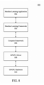
- the processing subsystem 101 includes one or more parallel processor(s) 112 coupled to memory hub 105 via a bus or other communication link 113.
- the communication link 113 may be one of any number of standards based communication link technologies or protocols, such as, but not limited to PCI Express, or may be a vendor specific communications interface or communications fabric.
- the one or more parallel processor(s) 112 form a computationally focused parallel or vector processing system that an include a large number of processing cores and/or processing clusters, such as a many integrated core (MIC) processor.
- the one or more parallel processor(s) 112 form a graphics processing subsystem that can output pixels to one of the one or more display device(s) 110A coupled via the I/O Hub 107.
- the one or more parallel processor(s) 112 can also include a display controller and display interface (not shown) to enable a direct connection to one or more display device(s) 110B.
- the computing system 100 can include other components not explicitly shown, including USB or other port connections, optical storage drives, video capture devices, and the like, may also be connected to the I/O hub 107.
- Communication paths interconnecting the various components in Figure 1 may be implemented using any suitable protocols, such as PCI (Peripheral Component Interconnect) based protocols (e.g., PCI-Express), or any other bus or point-to-point communication interfaces and/or protocol(s), such as the NV-Link high-speed interconnect, or interconnect protocols known in the art.
- PCI Peripheral Component Interconnect
- PCI-Express PCI-Express
- NV-Link high-speed interconnect, or interconnect protocols known in the art.
- the I/O hub 107 and memory hub 105 may be integrated into a single chip.
- Some embodiments may include two or more sets of processor(s) 102 attached via multiple sockets, which can couple with two or more instances of the parallel processor(s) 112.
- different clusters 214A-214N of the processing cluster array 212 can be allocated for processing different types of programs or for performing different types of computations.
- the processing cluster array 212 can be configured to perform various types of parallel processing operations.
- the processing cluster array 212 is configured to perform general-purpose parallel compute operations.
- the processing cluster array 212 can include logic to execute processing tasks including filtering of video and/or audio data, and/or modeling operations, including physics operations, and performing data transformations.
- the processing cluster array 212 is configured to perform parallel graphics processing operations.
- the processing cluster array 212 can include additional logic to support the execution of such graphics processing operations, including, but not limited to texture sampling logic to perform texture operations, as well as tessellation logic and other vertex processing logic.
- the processing cluster array 212 can be configured to execute graphics processing related shader programs such as, but not limited to vertex shaders, tessellation shaders, geometry shaders, and pixel shaders.
- the parallel processing unit 202 can transfer data from system memory via the I/O unit 204 for processing. During processing the transferred data can be stored to on-chip memory (e.g., parallel processor memory 222) during processing, then written back to system memory.
- the scheduler 210 can be configured to divide the processing workload into approximately equal sized tasks, to better enable distribution of the graphics processing operations to multiple clusters 214A-214N of the processing cluster array 212.
- portions of the processing cluster array 212 can be configured to perform different types of processing. For example, a first portion may be configured to perform vertex shading and topology generation, a second portion may be configured to perform tessellation and geometry shading, and a third portion may be configured to perform pixel shading or other screen space operations, to produce a rendered image for display.
- Intermediate data produced by one or more of the clusters 214A-214N may be stored in buffers to allow the intermediate data to be transmitted between clusters 214A-214N for further processing.
- the memory crossbar 216 has a connection to the memory interface 218 to communicate with the I/O unit 204, as well as a connection to a local instance of the parallel processor memory 222, enabling the processing units within the different processing clusters 214A-214N to communicate with system memory or other memory that is not local to the parallel processing unit 202.
- the memory crossbar 216 can use virtual channels to separate traffic streams between the clusters 214A-214N and the partition units 220A-220N.
- the processed graphics data may be displayed on display device, such as one of the one or more display device(s) 110 of Figure 1 , routed for further processing by the processor(s) 102, or routed for further processing by one of the processing entities within the parallel processor 200 of Figure 2A .
- FIG. 2C is a block diagram of a processing cluster 214 within a parallel processing unit, according to an embodiment.
- the processing cluster is an instance of one of the processing clusters 214A-214N of Figure 2 .
- the processing cluster 214 can be configured to execute many threads in parallel, where the term "thread” refers to an instance of a particular program executing on a particular set of input data.
- SIMD single-instruction, multiple-data
- the instructions transmitted to the processing cluster 214 constitutes a thread.
- a set of threads executing across the set of parallel processing engines is a thread group.
- a thread group executes the same program on different input data.
- Each thread within a thread group can be assigned to a different processing engine within a graphics multiprocessor 234.
- a thread group may include fewer threads than the number of processing engines within the graphics multiprocessor 234. When a thread group includes fewer threads than the number of processing engines, one or more of the processing engines may be idle during cycles in which that thread group is being processed.
- a thread group may also include more threads than the number of processing engines within the graphics multiprocessor 234. When the thread group includes more threads than the number of processing engines within the graphics multiprocessor 234, processing can be performed over consecutive clock cycles. In one embodiment multiple thread groups can be executed concurrently on a graphics multiprocessor 234.
- FIG. 2D shows a graphics multiprocessor 234, according to one embodiment.
- the graphics multiprocessor 234 couples with the pipeline manager 232 of the processing cluster 214.
- the graphics multiprocessor 234 has an execution pipeline including but not limited to an instruction cache 252, an instruction unit 254, an address mapping unit 256, a register file 258, one or more general purpose graphics processing unit (GPGPU) cores 262, and one or more load/store units 266.
- the GPGPU cores 262 and load/store units 266 are coupled with cache memory 272 and shared memory 270 via a memory and cache interconnect 268.
- the instruction cache 252 receives a stream of instructions to execute from the pipeline manager 232.
- the instructions are cached in the instruction cache 252 and dispatched for execution by the instruction unit 254.
- the instruction unit 254 can dispatch instructions as thread groups (e.g., warps), with each thread of the thread group assigned to a different execution unit within GPGPU core 262.
- An instruction can access any of a local, shared, or global address space by specifying an address within a unified address space.
- the address mapping unit 256 can be used to translate addresses in the unified address space into a distinct memory address that can be accessed by the load/store units 266.
- the memory and cache interconnect 268 is an interconnect network that connects each of the functional units of the graphics multiprocessor 324 to the register file 258 and to the shared memory 270.
- the memory and cache interconnect 268 is a crossbar interconnect that allows the load/store unit 266 to implement load and store operations between the shared memory 270 and the register file 258.
- the register file 258 can operate at the same frequency as the GPGPU cores 262, thus data transfer between the GPGPU cores 262 and the register file 258 is very low latency.
- the shared memory 270 can be used to enable communication between threads that execute on the functional units within the graphics multiprocessor 234.
- FIGS 3A-3B illustrate additional graphics multiprocessors, according to embodiments.
- the illustrated graphics multiprocessors 325, 350 are variants of the graphics multiprocessor 234 of Figure 2C .
- the illustrated graphics multiprocessors 325, 350 can be configured as a streaming multiprocessor (SM) capable of simultaneous execution of a large number of execution threads.
- SM streaming multiprocessor
- any properly configured processing unit including, without limitation, one or more mobile application processors, one or more desktop or server central processing units (CPUs) including multi-core CPUs, one or more parallel processing units, such as the parallel processing unit 202 of Figure 2 , as well as one or more graphics processors or special purpose processing units.
- processors including, without limitation, one or more mobile application processors, one or more desktop or server central processing units (CPUs) including multi-core CPUs, one or more parallel processing units, such as the parallel processing unit 202 of Figure 2 , as well as one or more graphics processors or special purpose processing units.
- the processor cores may allocate work to the GPU in the form of sequences of commands/instructions contained in a work descriptor.
- the GPU then uses dedicated circuitry/logic for efficiently processing these commands/instructions.
- two or more of the GPUs 410-413 are interconnected over high-speed links 444-445, which may be implemented using the same or different protocols/links than those used for high-speed links 440-443.
- two or more of the multi-core processors 405-406 may be connected over high speed link 433 which may be symmetric multi-processor (SMP) buses operating at 20GB/s, 30GB/s, 120GB/s or higher.
- SMP symmetric multi-processor
- each multi-core processor 405-406 is communicatively coupled to a processor memory 401-402, via memory interconnects 430-431, respectively, and each GPU 410-413 is communicatively coupled to GPU memory 420-423 over GPU memory interconnects 450-453, respectively.
- the memory interconnects 430-431 and 450-453 may utilize the same or different memory access technologies.
- processors 405-406 and GPUs 410-413 may be physically coupled to a particular memory 401-402, 420-423, respectively, a unified memory architecture may be implemented in which the same virtual system address space (also referred to as the "effective address" space) is distributed among all of the various physical memories.
- processor memories 401-402 may each comprise 64GB of the system memory address space
- GPU memories 420-423 may each comprise 32GB of the system memory address space (resulting in a total of 256GB addressable memory in this example).
- FIG. 4B illustrates additional details for an interconnection between a multi-core processor 407 and a graphics acceleration module 446 in accordance with one embodiment.
- the graphics acceleration module 446 may include one or more GPU chips integrated on a line card which is coupled to the processor 407 via the high-speed link 440.
- the graphics acceleration module 446 may be integrated on the same package or chip as the processor 407.
- the illustrated processor 407 includes a plurality of cores 460A-460D, each with a translation lookaside buffer 461A-461D and one or more caches 462A-462D.
- the cores may include various other components for executing instructions and processing data which are not illustrated to avoid obscuring the underlying principles of the invention (e.g., instruction fetch units, branch prediction units, decoders, execution units, reorder buffers, etc.).
- the caches 462A-462D may comprise level 1 (L1) and level 2 (L2) caches.
- one or more shared caches 426 may be included in the caching hierarchy and shared by sets of the cores 460A-460D.
- the accelerator integration circuit 436 includes a memory management unit (MMU) 439 for performing various memory management functions such as virtual-to-physical memory translations (also referred to as effective-to-real memory translations) and memory access protocols for accessing system memory 441.
- the MMU 439 may also include a translation lookaside buffer (TLB) (not shown) for caching the virtual/effective to physical/real address translations.
- a cache 438 stores commands and data for efficient access by the graphics processing engines 431-432, N.
- the data stored in cache 438 and graphics memories 433-434, N is kept coherent with the core caches 462A-462D, 456 and system memory 411.
- proxy circuit 425 which takes part in the cache coherency mechanism on behalf of cache 438 and memories 433-434, N (e.g., sending updates to the cache 438 related to modifications/accesses of cache lines on processor caches 462A-462D, 456 and receiving updates from the cache 438).
- virtual/effective addresses from a graphics processing engine 431 are translated to real/physical addresses in system memory 411 by the MMU 439.
- One embodiment of the accelerator integration circuit 436 supports multiple (e.g., 4, 8, 16) graphics accelerator modules 446 and/or other accelerator devices.
- the graphics accelerator module 446 may be dedicated to a single application executed on the processor 407 or may be shared between multiple applications.
- a virtualized graphics execution environment is presented in which the resources of the graphics processing engines 431-432, N are shared with multiple applications or virtual machines (VMs).
- the resources may be subdivided into "slices" which are allocated to different VMs and/or applications based on the processing requirements and priorities associated with the VMs and/or applications.
- biasing techniques are used to ensure that the data stored in graphics memories 433-434, M is data which will be used most frequently by the graphics processing engines 431-432, N and preferably not used by the cores 460A-460D (at least not frequently).
- the biasing mechanism attempts to keep data needed by the cores (and preferably not the graphics processing engines 431-432, N) within the caches 462A-462D, 456 of the cores and system memory 411.
- the graphics processing engines 431-432, N may be shared by multiple VM/application partitions.
- the shared models require a system hypervisor to virtualize the graphics processing engines 431-432, N to allow access by each operating system.
- the graphics processing engines 431-432, N are owned by the operating system. In both cases, the operating system can virtualize the graphics processing engines 431-432, N to provide access to each process or application.
- Figure 4D illustrates an exemplary accelerator integration slice 490.
- a "slice” comprises a specified portion of the processing resources of the accelerator integration circuit 436.
- Application effective address space 482 within system memory 411 stores process elements 483.
- the process elements 483 are stored in response to GPU invocations 481 from applications 480 executed on the processor 407.
- a process element 483 contains the process state for the corresponding application 480.
- a work descriptor (WD) 484 contained in the process element 483 can be a single job requested by an application or may contain a pointer to a queue of jobs. In the latter case, the WD 484 is a pointer to the job request queue in the application's address space 482.
- the dedicated-process programming model is implementation-specific.
- a single process owns the graphics acceleration module 446 or an individual graphics processing engine 431. Because the graphics acceleration module 446 is owned by a single process, the hypervisor initializes the accelerator integration circuit 436 for the owning partition and the operating system initializes the accelerator integration circuit 436 for the owning process at the time when the graphics acceleration module 446 is assigned.
- the shared programming models allow for all or a subset of processes from all or a subset of partitions in the system to use a graphics acceleration module 446.
- one embodiment of the invention employs a unified memory addressable via a common virtual memory address space used to access the physical processor memories 401-402 and GPU memories 420-423.
- operations executed on the GPUs 410-413 utilize the same virtual/effective memory address space to access the processors memories 401-402 and vice versa, thereby simplifying programmability.
- a first portion of the virtual/effective address space is allocated to the processor memory 401, a second portion to the second processor memory 402, a third portion to the GPU memory 420, and so on.
- the entire virtual/effective memory space (sometimes referred to as the effective address space) is thereby distributed across each of the processor memories 401-402 and GPU memories 420-423, allowing any processor or GPU to access any physical memory with a virtual address mapped to that memory.
- the bias table entry associated with each access to the GPU-attached memory 420-423 is accessed prior the actual access to the GPU memory, causing the following operations.
- First, local requests from the GPU 410-413 that find their page in GPU bias are forwarded directly to a corresponding GPU memory 420-423.
- Local requests from the GPU that find their page in host bias are forwarded to the processor 405 (e.g., over a high speed link as discussed above).
- requests from the processor 405 that find the requested page in host processor bias complete the request like a normal memory read.
- requests directed to a GPU-biased page may be forwarded to the GPU 410-413. The GPU may then transition the page to a host processor bias if it is not currently using the page.
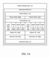
- a shader unit (e.g., graphics multiprocessor 234 of Figure 3 ) may be configured to perform the functions of one or more of a vertex processing unit 504, a tessellation control processing unit 508, a tessellation evaluation processing unit 512, a geometry processing unit 516, and a fragment/pixel processing unit 524.
- the functions of data assembler 502, primitive assemblers 506, 514, 518, tessellation unit 510, rasterizer 522, and raster operations unit 526 may also be performed by other processing engines within a processing cluster (e.g., processing cluster 214 of Figure 3 ) and a corresponding partition unit (e.g., partition unit 220A-220N of Figure 2 ).
- the graphics processing pipeline 500 may also be implemented using dedicated processing units for one or more functions.
- one or more portions of the graphics processing pipeline 500 can be performed by parallel processing logic within a general-purpose processor (e.g., CPU).
- one or more portions of the graphics processing pipeline 500 can access on-chip memory (e.g., parallel processor memory 222 as in Figure 2 ) via a memory interface 528, which may be an instance of the memory interface 218 of Figure 2 .
- a second instance of a primitive assembler 514 receives vertex attributes from the tessellation evaluation processing unit 512, reading stored vertex attributes as needed, and constructs graphics primitives for processing by the geometry processing unit 516.
- the geometry processing unit 516 is a programmable execution unit that executes geometry shader programs to transform graphics primitives received from primitive assembler 514 as specified by the geometry shader programs.
- the geometry processing unit 516 is programmed to subdivide the graphics primitives into one or more new graphics primitives and calculate parameters used to rasterize the new graphics primitives.
- the raster operations unit 526 is a processing unit that performs raster operations including, but not limited to stencil, z test, blending, and the like, and outputs pixel data as processed graphics data to be stored in graphics memory (e.g., parallel processor memory 222 as in Figure 1 , to be displayed on the one or more display device(s) 110 or for further processing by one of the one or more processor(s) 102 or parallel processor(s)112.
- the raster operations unit 526 is configured to compress z or color data that is written to memory and decompress z or color data that is read from memory.
- term “user” may be interchangeably referred to as “viewer”, “observer”, “person”, “individual”, “end-user”, and/or the like. It is to be noted that throughout this document, terms like “graphics domain” may be referenced interchangeably with “graphics processing unit”, “graphics processor”, or simply “GPU” and similarly, “CPU domain” or “host domain” may be referenced interchangeably with “computer processing unit”, “application processor”, or simply “CPU”.
- Computing device 600 may include any number and type of communication devices, such as large computing systems, such as server computers, desktop computers, etc., and may further include set-top boxes (e.g., Internet-based cable television set-top boxes, etc.), global positioning system (GPS)-based devices, etc.
- Computing device 600 may include mobile computing devices serving as communication devices, such as cellular phones including smartphones, personal digital assistants (PDAs), tablet computers, laptop computers, e-readers, smart televisions, television platforms, wearable devices (e.g., glasses, watches, bracelets, smartcards, jewelry, clothing items, etc.), media players, etc.
- computing device 600 may include any number and type of hardware and/or software components, such as (without limitation) GPU 614, graphics driver (also referred to as “GPU driver”, “graphics driver logic”, “driver logic”, user-mode driver (UMD), UMD, user-mode driver framework (UMDF), UMDF, or simply “driver”) 616, CPU 612, memory 608, network devices, drivers, or the like, as well as input/output (I/O) sources 604, such as touchscreens, touch panels, touch pads, virtual or regular keyboards, virtual or regular mice, ports, connectors, etc.
- graphics driver also referred to as "GPU driver”, “graphics driver logic”, “driver logic”, user-mode driver (UMD), UMD, user-mode driver framework (UMDF), UMDF, or simply “driver”
- CPU 612 memory 608, network devices, drivers, or the like
- I/O input/output
- memory 608 may include a random access memory (RAM) comprising application database having object information.
- RAM random access memory
- a memory controller hub such as memory hub 105 of Figure 1 , may access data in the RAM and forward it to GPU 614 for graphics pipeline processing.
- RAM may include double data rate RAM (DDR RAM), extended data output RAM (EDO RAM), etc.
- CPU 612 interacts with a hardware graphics pipeline to share graphics pipelining functionality.
- System memory 608 may be made available to other components within the computing device 600.
- any data e.g., input graphics data
- the computing device 600 e.g., keyboard and mouse, printer port, Local Area Network (LAN) port, modem port, etc.
- an internal storage element of the computer device 600 e.g., hard disk drive
- data that a software program determines should be sent from the computing device 600 to an outside entity through one of the computing system interfaces, or stored into an internal storage element is often temporarily queued in system memory 608 prior to its being transmitted or stored.
- an ICH may be used for ensuring that such data is properly passed between the system memory 608 and its appropriate corresponding computing system interface (and internal storage device if the computing system is so designed) and may have bi-directional point-to-point links between itself and the observed I/O sources/devices 604.
- an MCH may be used for managing the various contending requests for system memory 608 accesses amongst CPU 612 and GPU 614, interfaces and internal storage elements that may proximately arise in time with respect to one another.
- I/O sources 604 may include one or more I/O devices that are implemented for transferring data to and/or from computing device 600 (e.g., a networking adapter); or, for a large scale non-volatile storage within computing device 600 (e.g., hard disk drive).
- User input device including alphanumeric and other keys, may be used to communicate information and command selections to GPU 614.
- cursor control such as a mouse, a trackball, a touchscreen, a touchpad, or cursor direction keys to communicate direction information and command selections to GPU 614 and to control cursor movement on the display device.
- Camera and microphone arrays of computer device 600 may be employed to observe gestures, record audio and video and to receive and transmit visual and audio commands.
- computing device 600 may vary from implementation to implementation depending upon numerous factors, such as price constraints, performance requirements, technological improvements, or other circumstances.
- Examples of the electronic device or computer system 600 may include (without limitation) a mobile device, a personal digital assistant, a mobile computing device, a smartphone, a cellular telephone, a handset, a one-way pager, a two-way pager, a messaging device, a computer, a personal computer (PC), a desktop computer, a laptop computer, a notebook computer, a handheld computer, a tablet computer, a server, a server array or server farm, a web server, a network server, an Internet server, a work station, a mini-computer, a main frame computer, a supercomputer, a network appliance, a web appliance, a distributed computing system, multiprocessor systems, processor-based systems, consumer electronics, programmable consumer electronics, television, digital television, set top box,
- Embodiments may be implemented as any or a combination of: one or more microchips or integrated circuits interconnected using a parentboard, hardwired logic, software stored by a memory device and executed by a microprocessor, firmware, an application specific integrated circuit (ASIC), and/or a field programmable gate array (FPGA).
- logic may include, by way of example, software or hardware and/or combinations of software and hardware.
- embodiments may be downloaded as a computer program product, wherein the program may be transferred from a remote computer (e.g., a server) to a requesting computer (e.g., a client) by way of one or more data signals embodied in and/or modulated by a carrier wave or other propagation medium via a communication link (e.g., a modem and/or network connection).
- a remote computer e.g., a server
- a requesting computer e.g., a client
- a communication link e.g., a modem and/or network connection
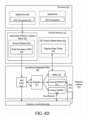
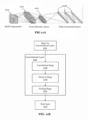
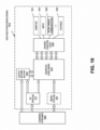
- Figure 7A is a flow diagram illustrating one embodiment of a CNN optimization process implemented by pruning mechanism 613.
- the CNN model is expanded into its elementary operations, which typically includes a significant quantity of multiply + add instructions.
- the expanded multiply instructions are predominantly defined as input_var * weight_var operations.
- the weight variable becomes constant during inference once the model has been trained. Further, each output variable of the network is generated by a series of multiply-adds.
- conditional branches in the model are optimized.
- the instruction list is traversed in order to prune (or optimize) the instruction list.
- the instruction list is optimized by eliminating all branches that are descended from 0 weight values. Additionally, the instruction may be optimized by disregarding branches having 1 weight values.
- Other embodiments may include a performance of additional optimization processes to reduce the total instruction count. For example, threshold based pruning may also be implemented. In such an embodiment, branches within a predetermined threshold of a 0 weight value is eliminated, while branches within a predetermined threshold of a 1 weight value is skipped.
- compression may be implemented using a loop replacement process. However other embodiments may feature different types of compression algorithms (e.g., applying a type of zip style compression on the instruction set).
- an executable application to perform the instructions in the reduced instruction is generated.
- a compiler or function generator
- Such an embodiment involves separating and scheduling instructions to make full use of all available GPU 614 hardware (e.g., cores etc.).
- optimization mechanism 610 also includes primitives 615 implemented for quantization and de-quantization convolution operations provided at a CNN.
- the primitives are instruction set architecture (ISA) or low level functions that set up a quantization step for a batch of operations, and provide other preparation operations to set a quantization table if the quantization is not uniform.
- the primitives include a convert operation, which may be a SIMD instruction to operate on packed data. Since the quantized convolution results often need to be converted to floating point for normalization operations, primitives 615 also include de-quantization operations.
- Figure 7B illustrates one embodiment of a list of primitives 615.
- a set of de-quantization to perform the opposite conversions.
- FPUs and integer ALUs within GPU 614 are configured to support primitives 615.
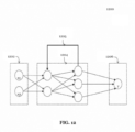
- Data received at the nodes of an input layer of a feedforward network are propagated (i.e., "fed forward") to the nodes of the output layer via an activation function that calculates the states of the nodes of each successive layer in the network based on coefficients ("weights") respectively associated with each of the edges connecting the layers.
- the output from the neural network algorithm can take various forms.
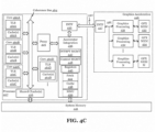
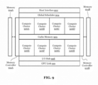
- the GPGPU 900 includes a host interface 902 to enable a connection with a host processor.
- the host interface 902 is a PCI Express interface.
- the host interface can also be a vendor specific communications interface or communications fabric.
- the GPGPU 900 receives commands from the host processor and uses a global scheduler 904 to distribute execution threads associated with those commands to a set of compute clusters 906A-H.
- the compute clusters 906A-H share a cache memory 908.
- the cache memory 908 can serve as a higher-level cache for cache memories within the compute clusters 906A-H.
- each compute cluster GPLAB06A-H includes a set of graphics multiprocessors, such as the graphics multiprocessor 400 of Figure 4A .
- the graphics multiprocessors of the compute cluster multiple types of integer and floating point logic units that can perform computational operations at a range of precisions including suited for machine learning computations.
- at least a subset of the floating point units in each of the compute clusters 906A-H can be configured to perform 16-bit or 32-bit floating point operations, while a different subset of the floating point units can be configured to perform 64-bit floating point operations.
- the illustrated configuration of the GPGPU 900 can be configured to train neural networks
- one embodiment provides alternate configuration of the GPGPU 900 that can be configured for deployment within a high performance or low power inferencing platform.
- the GPGPU 900 includes fewer of the compute clusters 906A-H relative to the training configuration. Additionally, memory technology associated with the memory 914A-B may differ between inferencing and training configurations.
- the inferencing configuration of the GPGPU 900 can support inferencing specific instructions.
- an inferencing configuration can provide support for one or more 8-bit integer dot product instructions, which are commonly used during inferencing operations for deployed neural networks.
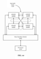
- FIG 10 illustrates a multi-GPU computing system 1000, according to an embodiment.
- the multi-GPU computing system 1000 can include a processor 1002 coupled to multiple GPGPUs 1006A-D via a host interface switch 1004.
- the host interface switch 1004 in one embodiment, is a PCI express switch device that couples the processor 1002 to a PCI express bus over which the processor 1002 can communicate with the set of GPGPUs 1006A-D.
- Each of the multiple GPGPUs 1006A-D can be an instance of the GPGPU 900 of Figure 9 .
- the GPGPUs 1006A-D can interconnect via a set of high-speed point to point GPU to GPU links 1016.
- the high-speed GPU to GPU links can connect to each of the GPGPUs 1006A-D via a dedicated GPU link, such as the GPU link 910 as in Figure 9 .
- the P2P GPU links 1016 enable direct communication between each of the GPGPUs 1006A-D without requiring communication over the host interface bus to which the processor 1002 is connected. With GPU-to-GPU traffic directed to the P2P GPU links, the host interface bus remains available for system memory access or to communicate with other instances of the multi-GPU computing system 1000, for example, via one or more network devices. While in the illustrated embodiment the GPGPUs 1006A-D connect to the processor 1002 via the host interface switch 1004, in one embodiment the processor 1002 includes direct support for the P2P GPU links 1016 and can connect directly to the GPGPUs 1006A-D.
- the computing architecture provided by embodiments described herein can be configured to perform the types of parallel processing that is particularly suited for training and deploying neural networks for machine learning.
- a neural network can be generalized as a network of functions having a graph relationship. As is well-known in the art, there are a variety of types of neural network implementations used in machine learning.
- One exemplary type of neural network is the feedforward network, as previously described.
- Convolution is a specialized kind of mathematical operation performed by two functions to produce a third function that is a modified version of one of the two original functions.
- the first function to the convolution can be referred to as the input, while the second function can be referred to as the convolution kernel.
- the output may be referred to as the feature map.
- the input to a convolution layer can be a multidimensional array of data that defines the various color components of an input image.
- the convolution kernel can be a multidimensional array of parameters, where the parameters are adapted by the training process for the neural network.
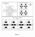
- Deep learning is machine learning using deep neural networks.
- the deep neural networks used in deep learning are artificial neural networks composed of multiple hidden layers, as opposed to shallow neural networks that include only a single hidden layer. Deeper neural networks are generally more computationally intensive to train. However, the additional hidden layers of the network enable multistep pattern recognition that results in reduced output error relative to shallow machine learning techniques.
- Deep neural networks used in deep learning typically include a front-end network to perform feature recognition coupled to a back-end network which represents a mathematical model that can perform operations (e.g., object classification, speech recognition, etc.) based on the feature representation provided to the model.
- Deep learning enables machine learning to be performed without requiring hand crafted feature engineering to be performed for the model.
- deep neural networks can learn features based on statistical structure or correlation within the input data.
- the learned features can be provided to a mathematical model that can map detected features to an output.
- the mathematical model used by the network is generally specialized for the specific task to be performed, and different models will be used to perform different task.
- the pooling stage 1120 uses a pooling function that replaces the output of the convolutional layer 1106 with a summary statistic of the nearby outputs.
- the pooling function can be used to introduce translation invariance into the neural network, such that small translations to the input do not change the pooled outputs. Invariance to local translation can be useful in scenarios where the presence of a feature in the input data is more important than the precise location of the feature.
- Various types of pooling functions can be used during the pooling stage 1120, including max pooling, average pooling, and l2-norm pooling. Additionally, some CNN implementations do not include a pooling stage. Instead, such implementations substitute and additional convolution stage having an increased stride relative to previous convolution stages.
- the one or more processors 1602 each include one or more processor cores 1607 to process instructions which, when executed, perform operations for system and user software.
- each of the one or more processor cores 1607 is configured to process a specific instruction set 1609.
- instruction set 1609 may facilitate Complex Instruction Set Computing (CISC), Reduced Instruction Set Computing (RISC), or computing via a Very Long Instruction Word (VLIW).
- Multiple processor cores 1607 may each process a different instruction set 1609, which may include instructions to facilitate the emulation of other instruction sets.
- Processor core 1607 may also include other processing devices, such a Digital Signal Processor (DSP).
- DSP Digital Signal Processor
- Memory device 1620 can be a dynamic random access memory (DRAM) device, a static random access memory (SRAM) device, flash memory device, phase-change memory device, or some other memory device having suitable performance to serve as process memory.
- the memory device 1620 can operate as system memory for the system 1600, to store data 1622 and instructions 1621 for use when the one or more processors 1602 executes an application or process.
- Memory controller hub 1616 also couples with an optional external graphics processor 1612, which may communicate with the one or more graphics processors 1608 in processors 1602 to perform graphics and media operations.
- processor 1700 additionally includes graphics processor 1708 to execute graphics processing operations.
- the graphics processor 1708 couples with the set of shared cache units 1706, and the system agent core 1710, including the one or more integrated memory controllers 1714.
- a display controller 1711 is coupled with the graphics processor 1708 to drive graphics processor output to one or more coupled displays.
- display controller 1711 may be a separate module coupled with the graphics processor via at least one interconnect, or may be integrated within the graphics processor 1708 or system agent core 1710.
- processor cores 1702A-1702N are homogenous cores executing the same instruction set architecture.
- processor cores 1702A-1702N are heterogeneous in terms of instruction set architecture (ISA), where one or more of processor cores 1702A-1702N execute a first instruction set, while at least one of the other cores executes a subset of the first instruction set or a different instruction set.
- processor cores 1702A-1702N are heterogeneous in terms of micro architecture, where one or more cores having a relatively higher power consumption couple with one or more power cores having a lower power consumption.
- processor 1700 can be implemented on one or more chips or as an SoC integrated circuit having the illustrated components, in addition to other components.
- graphics processor 2000 receives batches of commands via ring interconnect 2002. The incoming commands are interpreted by a command streamer 2003 in the pipeline front-end 2004.
- graphics processor 2000 includes scalable execution logic to perform 3D geometry processing and media processing via the graphics core(s) 2080A-2080N.
- command streamer 2003 supplies commands to geometry pipeline 2036.
- command streamer 2003 supplies the commands to a video front end 2034, which couples with a media engine 2037.
- media engine 2037 includes a Video Quality Engine (VQE) 2030 for video and image post-processing and a multi-format encode/decode (MFX) 2033 engine to provide hardware-accelerated media data encode and decode.
- geometry pipeline 2036 and media engine 2037 each generate execution threads for the thread execution resources provided by at least one graphics core 2080A.
- graphics processor 2000 includes scalable thread execution resources featuring modular cores 2080A-2080N (sometimes referred to as core slices), each having multiple sub-cores 2050A-550N, 2060A-2060N (sometimes referred to as core sub-slices).
- graphics processor 2000 can have any number of graphics cores 2080A through 2080N.
- graphics processor 2000 includes a graphics core 2080A having at least a first sub-core 2050A and a second sub-core 2060A.
- the graphics processor is a low power processor with a single sub-core (e.g., 2050A).
- thread execution logic 2100 includes one or more connections to memory, such as system memory or cache memory, through one or more of instruction cache 2106, data port 2114, sampler 2110, and execution units 2108A-2108N.
- each execution unit e.g. 2108A
- the array of execution units 2108A-2108N is scalable to include any number individual execution units.
- complete geometric objects can be processed by a geometry shader 2319 via one or more threads dispatched to execution units 2352A-2352B, or can proceed directly to the clipper 2329.
- the geometry shader operates on entire geometric objects, rather than vertices or patches of vertices as in previous stages of the graphics pipeline. If the tessellation is disabled the geometry shader 2319 receives input from the vertex shader 2307. In some embodiments, geometry shader 2319 is programmable by a geometry shader program to perform geometry tessellation if the tessellation units are disabled.
- render output pipeline 2370 contains a rasterizer and depth test component 2373 that converts vertex-based objects into an associated pixel-based representation.
- the rasterizer logic includes a windower/masker unit to perform fixed function triangle and line rasterization.
- An associated render cache 2378 and depth cache 2379 are also available in some embodiments.
- a pixel operations component 2377 performs pixel-based operations on the data, though in some instances, pixel operations associated with 2D operations (e.g. bit block image transfers with blending) are performed by the 2D engine 2341, or substituted at display time by the display controller 2343 using overlay display planes.
- a shared L3 cache 2375 is available to all graphics components, allowing the sharing of data without the use of main system memory.
- Figure 24A is a block diagram illustrating a graphics processor command format 2400 according to some embodiments.
- Figure 24B is a block diagram illustrating a graphics processor command sequence 2410 according to an embodiment.
- the solid lined boxes in Figure 24A illustrate the components that are generally included in a graphics command while the dashed lines include components that are optional or that are only included in a sub-set of the graphics commands.
- the exemplary graphics processor command format 2400 of Figure 24A includes data fields to identify a target client 2402 of the command, a command operation code (opcode) 2404, and the relevant data 2406 for the command.
- opcode command operation code
- a sub-opcode 2405 and a command size 2408 are also included in some commands.
- client 2402 specifies the client unit of the graphics device that processes the command data.
- a graphics processor command parser examines the client field of each command to condition the further processing of the command and route the command data to the appropriate client unit.
- the graphics processor client units include a memory interface unit, a render unit, a 2D unit, a 3D unit, and a media unit. Each client unit has a corresponding processing pipeline that processes the commands. Once the command is received by the client unit, the client unit reads the opcode 2404 and, if present, sub-opcode 2405 to determine the operation to perform. The client unit performs the command using information in data field 2406.
- return buffer state commands 2416 are used to configure a set of return buffers for the respective pipelines to write data. Some pipeline operations require the allocation, selection, or configuration of one or more return buffers into which the operations write intermediate data during processing. In some embodiments, the graphics processor also uses one or more return buffers to store output data and to perform cross thread communication. In some embodiments, the return buffer state 2416 includes selecting the size and number of return buffers to use for a set of pipeline operations.
- high-level shaders are compiled into low-level shaders during the compilation of the 3D graphics application 2510.
- the shader instructions 2512 are provided in an intermediate form, such as a version of the Standard Portable Intermediate Representation (SPIR) used by the Vulkan API.
- SPIR Standard Portable Intermediate Representation
- user mode graphics driver 2526 contains a back-end shader compiler 2527 to convert the shader instructions 2512 into a hardware specific representation.
- shader instructions 2512 in the GLSL high-level language are passed to a user mode graphics driver 2526 for compilation.
- user mode graphics driver 2526 uses operating system kernel mode functions 2528 to communicate with a kernel mode graphics driver 2529.
- kernel mode graphics driver 2529 communicates with graphics processor 2532 to dispatch commands and instructions.
- the RTL design 2615 is an abstraction of the behavior of the integrated circuit that models the flow of digital signals between hardware registers, including the associated logic performed using the modeled digital signals.
- lower-level designs at the logic level or transistor level may also be created, designed, or synthesized. Thus, the particular details of the initial design and simulation may vary.
- the RTL design 2615 or equivalent may be further synthesized by the design facility into a hardware model 2620, which may be in a hardware description language (HDL), or some other representation of physical design data.
- the HDL may be further simulated or tested to verify the IP core design.
- the IP core design can be stored for delivery to a 3 rd party fabrication facility 2665 using non-volatile memory 2640 (e.g., hard disk, flash memory, or any non-volatile storage medium).
- the IP core design may be transmitted (e.g., via the Internet) over a wired connection 2650 or wireless connection 2660.
- the fabrication facility 2665 may then fabricate an integrated circuit that is based at least in part on the IP core design.
- the fabricated integrated circuit can be configured to perform operations in accordance with at least one embodiment described herein.
- Figure 28 is a block diagram illustrating an exemplary graphics processor 2810 of a system on a chip integrated circuit that may be fabricated using one or more IP cores, according to an embodiment.
- Graphics processor 2810 can be a variant of the graphics processor 2710 of Figure 27 .
- Graphics processor 2810 includes a vertex processor 2805 and one or more fragment processor(s) 2815A-2815N (e.g., 2815A, 2815B, 2815C, 2815D, through 2815N-1, and 2815N).
- Graphics processor 2810 can execute different shader programs via separate logic, such that the vertex processor 2805 is optimized to execute operations for vertex shader programs, while the one or more fragment processor(s) 2815A-2815N execute fragment (e.g., pixel) shading operations for fragment or pixel shader programs.
- the vertex processor 2805 performs the vertex processing stage of the 3D graphics pipeline and generates primitives and vertex data.
- the fragment processor(s) 2815A-2815N use the primitive and vertex data generated by the vertex processor 2805 to produce a framebuffer that is displayed on a display device.
- the fragment processor(s) 2815A-2815N are optimized to execute fragment shader programs as provided for in the OpenGL API, which may be used to perform similar operations as a pixel shader program as provided for in the Direct 3D API.
- Figure 29 is a block diagram illustrating an additional exemplary graphics processor 2910 of a system on a chip integrated circuit that may be fabricated using one or more IP cores, according to an embodiment.
- Graphics processor 2910 can be a variant of the graphics processor 2710 of Figure 27 .
- Graphics processor 2910 includes the one or more MMU(s) 2820A-2820B, caches 2825A-2825B, and circuit interconnects 2830A-2830B of the integrated circuit 2800 of Figure 28 .
- graphics processor 2910 includes an inter-core task manager 2905, which acts as a thread dispatcher to dispatch execution threads to one or more shader cores 2915A-2915N and a tiling unit 2918 to accelerate tiling operations for tile-based rendering, in which rendering operations for a scene are subdivided in image space, for example to exploit local spatial coherence within a scene or to optimize use of internal caches.
- inter-core task manager 2905 acts as a thread dispatcher to dispatch execution threads to one or more shader cores 2915A-2915N and a tiling unit 2918 to accelerate tiling operations for tile-based rendering, in which rendering operations for a scene are subdivided in image space, for example to exploit local spatial coherence within a scene or to optimize use of internal caches.
- the pruning logic further optimizes the list of instructions by eliminating branches in the CNN model having a weight value within a predetermined threshold of 0.
- the optimization logic further comprises a set of de-quantization primitives to convert the lower floating point or integer numbers into the N number of floating point numbers including FP32 and FP16, the primitives are instruction set architecture, ISA, or low level functions.
- an apparatus comprises means for performing the method.
Landscapes
- Engineering & Computer Science (AREA)
- Physics & Mathematics (AREA)
- Theoretical Computer Science (AREA)
- General Physics & Mathematics (AREA)
- Software Systems (AREA)
- Health & Medical Sciences (AREA)
- Life Sciences & Earth Sciences (AREA)
- Biomedical Technology (AREA)
- Biophysics (AREA)
- General Engineering & Computer Science (AREA)
- Computing Systems (AREA)
- Artificial Intelligence (AREA)
- General Health & Medical Sciences (AREA)
- Evolutionary Computation (AREA)
- Data Mining & Analysis (AREA)
- Mathematical Physics (AREA)
- Computational Linguistics (AREA)
- Molecular Biology (AREA)
- Neurology (AREA)
- Multimedia (AREA)
- Image Processing (AREA)
- Image Generation (AREA)
- Image Analysis (AREA)
- Complex Calculations (AREA)
- Management, Administration, Business Operations System, And Electronic Commerce (AREA)
- General Factory Administration (AREA)
Claims (7)
- Vorrichtung zur Optimierung eines Modells eines neuronalen Faltungsnetzwerks, CNN, nachdem das CNN-Modell vollständig trainiert wurde und bereit ist, eingesetzt zu werden, umfassend:eine Grafikverarbeitungseinheit, GPU, (614), die einen oder mehrere Grafikprozessoren aufweist;wobei die GPU (614) einen Optimierungsmechanismus (610) implementiert, der einen Beschneidungsmechanismus (613) aufweist, umdas trainierte CNN-Modell zu empfangen, wobei das trainierte CNN-Modell eine Netzwerktopologie aufweist, die unter Verwendung eines Trainingsdatensatzes ausgewählt wird, der ein Problem darstellt, das durch das CNN-Modell modelliert wird, und Gewichtungswerte angepasst werden, bis das CNN-Modell mit einem minimalen Fehler für alle Instanzen des Trainingsdatensatzes arbeitet;das trainierte CNN-Modell auf elementare Operationen zu erweitern (702), die eine Anzahl von Multiplikations-Additions-Anweisungen aufweisen;die Anzahl von Multiplikations-Additions-Anweisungen zu traversieren (704), um die Anzahl von Multiplikations-Additions-Anweisungen zu optimieren;wobei die Optimierung eine schwellenwertbasierte Optimierung ist, bei der Verzweigungen innerhalb eines vorbestimmten Schwellenwerts eines Gewichtungswerts von 0 eliminiert werden, während Verzweigungen innerhalb eines vorbestimmten Schwellenwerts eines Gewichtungswerts von 1 übersprungen werden.
- Vorrichtung nach Anspruch 1, wobei die GPU (614) den Optimierungsmechanismus (610) implementiert, um die Anzahl von Multiplikations-Additions-Anweisungen unter Verwendung eines Komprimierungsalgorithmus, der einen Schleifenersetzungsprozess aufweist, auf eine kleinere Darstellung zu komprimieren (706).
- Vorrichtung nach Anspruch 1, wobei die GPU (614) einen Compiler zum Erzeugen (708) einer ausführbaren Anwendung zum Durchführen der optimierten Anzahl von Multiplikations-Additions-Anweisungen aufweist, wobei die optimierte Anzahl von Multiplikations-Additions-Anweisungen eine reduzierte Anzahl von Multiplikations-Additions-Anweisungen aufweist.
- Verfahren zur Optimierung eines Modells eines neuronalen Faltungsnetzwerks, CNN, nachdem das CNN-Modell vollständig trainiert wurde und bereit ist, eingesetzt zu werden, umfassend:Empfangen des trainierten CNN-Modells durch eine Grafikverarbeitungseinheit, GPU, (614), wobei das trainierte CNN-Modell eine Netzwerktopologie aufweist, die unter Verwendung eines Trainingsdatensatzes ausgewählt wird, der ein Problem darstellt, das durch das CNN-Modell modelliert wird, und Gewichtungswerte angepasst werden, bis das CNN-Modell mit einem minimalen Fehler für alle Instanzen des Trainingsdatensatzes arbeitet;Erweitern (702) des trainierten CNN-Modells durch die GPU (614) auf elementare Operationen, die eine Anzahl von Multiplikations-Additions-Anweisungen aufweisen;Traversieren (704) der Anzahl von Multiplikations-Additions-Anweisungen durch die GPU (614), um die Anzahl von Multiplikations-Additions-Anweisungen zu optimieren, wobei die Optimierung eine schwellenwertbasierte Optimierung ist, bei der Verzweigungen innerhalb eines vorbestimmten Schwellenwerts eines Gewichtungswerts von 0 eliminiert werden, während Verzweigungen innerhalb eines vorbestimmten Schwellenwerts eines Gewichtungswerts von 1 übersprungen werden.
- Verfahren nach Anspruch 4, ferner umfassend Komprimieren (706) der Anzahl von Multiplikations-Additions-Anweisungen durch die GPU (614) unter Verwendung eines Komprimierungsalgorithmus, der einen Schleifenersetzungsprozess aufweist, auf eine kleinere Darstellung.
- Verfahren nach Anspruch 5, ferner umfassend Erzeugen (708) einer ausführbaren Anwendung durch einen Compiler der GPU (614) zum Durchführen der optimierten Anzahl von Multiplikations-Additions-Anweisungen, wobei die optimierte Anzahl von Multiplikations-Additions-Anweisungen eine reduzierte Anzahl von Multiplikations-Additions-Anweisungen aufweist.
- Mindestens ein computerlesbares Medium, das Anweisungen aufweist, die, wenn sie von einem oder mehreren Prozessoren ausgeführt werden, die Prozessoren veranlassen, das Verfahren nach einem der Ansprüche 4-6 durchzuführen.
Priority Applications (1)
| Application Number | Priority Date | Filing Date | Title |
|---|---|---|---|
| EP25167264.8A EP4553752A3 (de) | 2017-04-17 | 2018-03-23 | Mechanismus zur optimierung eines neuronalen faltungsnetzes |
Applications Claiming Priority (1)
| Application Number | Priority Date | Filing Date | Title |
|---|---|---|---|
| US15/488,551 US11934934B2 (en) | 2017-04-17 | 2017-04-17 | Convolutional neural network optimization mechanism |
Related Child Applications (1)
| Application Number | Title | Priority Date | Filing Date |
|---|---|---|---|
| EP25167264.8A Division EP4553752A3 (de) | 2017-04-17 | 2018-03-23 | Mechanismus zur optimierung eines neuronalen faltungsnetzes |
Publications (2)
| Publication Number | Publication Date |
|---|---|
| EP3392826A1 EP3392826A1 (de) | 2018-10-24 |
| EP3392826B1 true EP3392826B1 (de) | 2025-04-16 |
Family
ID=61952520
Family Applications (2)
| Application Number | Title | Priority Date | Filing Date |
|---|---|---|---|
| EP25167264.8A Pending EP4553752A3 (de) | 2017-04-17 | 2018-03-23 | Mechanismus zur optimierung eines neuronalen faltungsnetzes |
| EP18163810.7A Active EP3392826B1 (de) | 2017-04-17 | 2018-03-23 | Mechanismus zur optimierung eines neuronalen faltungsnetzwerks |
Family Applications Before (1)
| Application Number | Title | Priority Date | Filing Date |
|---|---|---|---|
| EP25167264.8A Pending EP4553752A3 (de) | 2017-04-17 | 2018-03-23 | Mechanismus zur optimierung eines neuronalen faltungsnetzes |
Country Status (5)
| Country | Link |
|---|---|
| US (4) | US11934934B2 (de) |
| EP (2) | EP4553752A3 (de) |
| CN (1) | CN108734272A (de) |
| ES (1) | ES3034673T3 (de) |
| PL (1) | PL3392826T3 (de) |
Families Citing this family (56)
| Publication number | Priority date | Publication date | Assignee | Title |
|---|---|---|---|---|
| CN110443351B (zh) | 2014-11-14 | 2021-05-28 | 谷歌有限责任公司 | 生成映像的自然语言描述 |
| US11010338B2 (en) * | 2017-04-06 | 2021-05-18 | Shanghai Cambricon Information Technology Co., Ltd | Data screening device and method |
| US11934934B2 (en) | 2017-04-17 | 2024-03-19 | Intel Corporation | Convolutional neural network optimization mechanism |
| US11113603B1 (en) | 2017-05-01 | 2021-09-07 | Perceive Corporation | Training network with discrete weight values |
| US11321604B2 (en) | 2017-06-21 | 2022-05-03 | Arm Ltd. | Systems and devices for compressing neural network parameters |
| US11275996B2 (en) * | 2017-06-21 | 2022-03-15 | Arm Ltd. | Systems and devices for formatting neural network parameters |
| EP3588392A4 (de) * | 2017-12-25 | 2020-05-20 | SONY Corporation | Informationsverarbeitungsvorrichtung, informationsverarbeitungsverfahren und programm |
| CN110045960B (zh) * | 2018-01-16 | 2022-02-18 | 腾讯科技(深圳)有限公司 | 基于芯片的指令集处理方法、装置及存储介质 |
| US11568227B1 (en) | 2018-04-20 | 2023-01-31 | Perceive Corporation | Neural network inference circuit read controller with multiple operational modes |
| US12093696B1 (en) | 2018-04-20 | 2024-09-17 | Perceive Corporation | Bus for transporting output values of a neural network layer to cores specified by configuration data |
| US11170289B1 (en) | 2018-04-20 | 2021-11-09 | Perceive Corporation | Computation of neural network node by neural network inference circuit |
| US11222257B1 (en) * | 2018-04-20 | 2022-01-11 | Perceive Corporation | Non-dot product computations on neural network inference circuit |
| US11210586B1 (en) | 2018-04-20 | 2021-12-28 | Perceive Corporation | Weight value decoder of neural network inference circuit |
| US10977338B1 (en) | 2018-04-20 | 2021-04-13 | Perceive Corporation | Reduced-area circuit for dot product computation |
| US11586910B1 (en) | 2018-04-20 | 2023-02-21 | Perceive Corporation | Write cache for neural network inference circuit |
| US11783167B1 (en) | 2018-04-20 | 2023-10-10 | Perceive Corporation | Data transfer for non-dot product computations on neural network inference circuit |
| US11531868B1 (en) | 2018-04-20 | 2022-12-20 | Perceive Corporation | Input value cache for temporarily storing input values |
| JP7287388B2 (ja) * | 2018-05-14 | 2023-06-06 | ソニーグループ株式会社 | 情報処理装置および情報処理方法 |
| KR102602195B1 (ko) * | 2018-10-30 | 2023-11-13 | 구글 엘엘씨 | 트레이닝된 장단기 메모리 신경망 양자화 |
| KR102621118B1 (ko) * | 2018-11-01 | 2024-01-04 | 삼성전자주식회사 | 영상 적응적 양자화 테이블을 이용한 영상의 부호화 장치 및 방법 |
| CN109550249B (zh) * | 2018-11-28 | 2022-04-29 | 腾讯科技(深圳)有限公司 | 一种目标对象的控制方法、装置及设备 |
| US11995532B2 (en) * | 2018-12-05 | 2024-05-28 | Arm Limited | Systems and devices for configuring neural network circuitry |
| US11995533B1 (en) | 2018-12-05 | 2024-05-28 | Perceive Corporation | Executing replicated neural network layers on inference circuit |
| US11347297B1 (en) | 2019-01-23 | 2022-05-31 | Perceive Corporation | Neural network inference circuit employing dynamic memory sleep |
| CN110069284B (zh) * | 2019-03-14 | 2023-05-05 | 梁磊 | 一种基于opu指令集的编译方法及编译器 |
| US11475308B2 (en) | 2019-03-15 | 2022-10-18 | Samsung Electronics Co., Ltd. | Jointly pruning and quantizing deep neural networks |
| CN110008028B (zh) * | 2019-04-10 | 2021-08-06 | 北京旷视科技有限公司 | 计算资源分配方法、装置、计算机设备和存储介质 |
| US12260317B1 (en) | 2019-05-21 | 2025-03-25 | Amazon Technologies, Inc. | Compiler for implementing gating functions for neural network configuration |
| CN110334802B (zh) * | 2019-05-23 | 2025-02-18 | 腾讯科技(深圳)有限公司 | 一种神经网络模型的构建方法、装置、设备及存储介质 |
| CN112085175B (zh) * | 2019-06-14 | 2024-05-03 | 华为技术有限公司 | 基于神经网络计算的数据处理方法和装置 |
| US11669585B2 (en) * | 2019-06-25 | 2023-06-06 | Apple Inc. | Optimizing binary convolutional neural networks |
| CN110348567B (zh) * | 2019-07-15 | 2022-10-25 | 北京大学深圳研究生院 | 一种基于自动寻址和递归信息整合的内存网络方法 |
| US10956776B2 (en) | 2019-08-06 | 2021-03-23 | Alibaba Group Holding Limited | 2D convolutional accelerator that generates 3D results |
| US11556768B2 (en) | 2019-10-31 | 2023-01-17 | Samsung Electronics Co., Ltd | Optimization of sparsified neural network layers for semi-digital crossbar architectures |
| JP7229905B2 (ja) * | 2019-12-05 | 2023-02-28 | 日立Astemo株式会社 | ニューラルネットワーク縮約装置およびその方法 |
| CN111240743B (zh) * | 2020-01-03 | 2022-06-03 | 格兰菲智能科技有限公司 | 人工智能集成电路 |
| DE102020202093A1 (de) * | 2020-02-19 | 2021-08-19 | Robert Bosch Gesellschaft mit beschränkter Haftung | Verfahren und Vorrichtung für maschinelles Lernen |
| US11615304B1 (en) * | 2020-03-05 | 2023-03-28 | Ambarella International Lp | Quantization aware training by constraining input |
| CN113779366B (zh) * | 2020-06-10 | 2023-06-27 | 北京超星未来科技有限公司 | 用于自动驾驶的神经网络架构自动优化部署方法及装置 |
| CN111738348B (zh) * | 2020-06-29 | 2023-07-11 | 南方电网科学研究院有限责任公司 | 一种电力数据异常检测方法和装置 |
| US11494787B2 (en) * | 2020-06-30 | 2022-11-08 | Optum, Inc. | Graph convolutional anomaly detection |
| CN116171437B (zh) * | 2020-10-21 | 2025-05-06 | 阿里巴巴集团控股有限公司 | 通过智能内存池进行嵌入的方法和系统 |
| CN112489088A (zh) * | 2020-12-15 | 2021-03-12 | 东北大学 | 一种基于记忆单元的孪生网络视觉跟踪方法 |
| CN112748998B (zh) * | 2021-01-21 | 2023-10-03 | 中南大学 | 一种移动端的卷积神经网络任务调度方法及系统 |
| US12159214B1 (en) | 2021-04-23 | 2024-12-03 | Perceive Corporation | Buffering of neural network inputs and outputs |
| CN113420623B (zh) * | 2021-06-09 | 2022-07-12 | 山东师范大学 | 基于自组织映射神经网络的5g基站检测方法及系统 |
| EP4392947A4 (de) * | 2021-08-27 | 2025-04-30 | Beko Europe Management S.r.l. | System zur identifizierung von lebensmitteltypen |
| US20230083345A1 (en) * | 2021-09-07 | 2023-03-16 | Nvidia Corporation | Multi-architecture execution graphs |
| KR102658912B1 (ko) * | 2021-09-24 | 2024-04-18 | 한국과학기술원 | 도메인별 최적화를 위한 생성 신경망의 에너지 효율적인 재학습 방법 |
| US11989142B2 (en) | 2021-12-10 | 2024-05-21 | Samsung Electronics Co., Ltd. | Efficient and concurrent model execution |
| US12197350B2 (en) | 2021-12-10 | 2025-01-14 | Samsung Electronics Co., Ltd. | Low-latency input data staging to execute kernels |
| US12443154B2 (en) * | 2022-03-18 | 2025-10-14 | Rockwell Automation Technologies, Inc. | Feature extraction integration with control programs |
| US12159140B2 (en) | 2022-04-28 | 2024-12-03 | Qualcomm Incorporated | Instruction set architecture for neural network quantization and packing |
| KR102737303B1 (ko) * | 2022-12-30 | 2024-12-03 | 주식회사 딥이티 | 인공지능 모델의 가속 연산을 위한 병렬 처리 장치 및 방법 |
| CN119538971A (zh) * | 2023-08-30 | 2025-02-28 | 英业达科技有限公司 | 加密深度神经网络模型的推论及转换方法 |
| WO2025193506A1 (en) * | 2024-03-13 | 2025-09-18 | Intel Corporation | Lookup table for small weight encodings |
Family Cites Families (17)
| Publication number | Priority date | Publication date | Assignee | Title |
|---|---|---|---|---|
| US7873812B1 (en) | 2004-04-05 | 2011-01-18 | Tibet MIMAR | Method and system for efficient matrix multiplication in a SIMD processor architecture |
| US8813057B2 (en) * | 2007-03-31 | 2014-08-19 | Intel Corporation | Branch pruning in architectures with speculation support |
| US20140072242A1 (en) * | 2012-09-10 | 2014-03-13 | Hao Wei | Method for increasing image resolution |
| US10223333B2 (en) | 2014-08-29 | 2019-03-05 | Nvidia Corporation | Performing multi-convolution operations in a parallel processing system |
| US10540957B2 (en) * | 2014-12-15 | 2020-01-21 | Baidu Usa Llc | Systems and methods for speech transcription |
| GB201511887D0 (en) | 2015-07-07 | 2015-08-19 | Touchtype Ltd | Improved artificial neural network for language modelling and prediction |
| US20190073582A1 (en) * | 2015-09-23 | 2019-03-07 | Yi Yang | Apparatus and method for local quantization for convolutional neural networks (cnns) |
| US11222263B2 (en) * | 2016-07-28 | 2022-01-11 | Samsung Electronics Co., Ltd. | Neural network method and apparatus |
| US10997496B2 (en) | 2016-08-11 | 2021-05-04 | Nvidia Corporation | Sparse convolutional neural network accelerator |
| US10891538B2 (en) * | 2016-08-11 | 2021-01-12 | Nvidia Corporation | Sparse convolutional neural network accelerator |
| US20180046903A1 (en) * | 2016-08-12 | 2018-02-15 | DeePhi Technology Co., Ltd. | Deep processing unit (dpu) for implementing an artificial neural network (ann) |
| US10621486B2 (en) | 2016-08-12 | 2020-04-14 | Beijing Deephi Intelligent Technology Co., Ltd. | Method for optimizing an artificial neural network (ANN) |
| EP3607741A4 (de) * | 2017-04-07 | 2020-12-09 | INTEL Corporation | Verfahren und systeme unter verwendung von kameravorrichtungen für tiefe neuronale kanal- und faltungsnetzbilder und formate |
| US11934934B2 (en) | 2017-04-17 | 2024-03-19 | Intel Corporation | Convolutional neural network optimization mechanism |
| US10403003B2 (en) | 2017-04-24 | 2019-09-03 | Intel Corporation | Compression mechanism |
| US20190050710A1 (en) | 2017-08-14 | 2019-02-14 | Midea Group Co., Ltd. | Adaptive bit-width reduction for neural networks |
| US11783200B2 (en) * | 2019-02-08 | 2023-10-10 | International Business Machines Corporation | Artificial neural network implementation in field-programmable gate arrays |
-
2017
- 2017-04-17 US US15/488,551 patent/US11934934B2/en active Active
-
2018
- 2018-03-23 ES ES18163810T patent/ES3034673T3/es active Active
- 2018-03-23 PL PL18163810.7T patent/PL3392826T3/pl unknown
- 2018-03-23 EP EP25167264.8A patent/EP4553752A3/de active Pending
- 2018-03-23 EP EP18163810.7A patent/EP3392826B1/de active Active
- 2018-04-16 CN CN201810337318.7A patent/CN108734272A/zh active Pending
-
2019
- 2019-02-22 US US16/283,021 patent/US11727246B2/en active Active
-
2021
- 2021-08-26 US US17/446,101 patent/US12020135B2/en active Active
-
2024
- 2024-02-07 US US18/435,528 patent/US20240256825A1/en active Pending
Non-Patent Citations (1)
| Title |
|---|
| RAJARAMAN V: "IEEE standard for floating point numbers", RESONANCE - JOURNAL OF SCIENCE EDUCATION, INDIAN ACADEMY OF SCIENCES, INDIA, vol. 21, no. 1, 11 February 2016 (2016-02-11), pages 11 - 30, XP035623571 * |
Also Published As
| Publication number | Publication date |
|---|---|
| EP4553752A3 (de) | 2025-07-16 |
| PL3392826T3 (pl) | 2025-07-28 |
| US20210397925A1 (en) | 2021-12-23 |
| US11727246B2 (en) | 2023-08-15 |
| ES3034673T3 (en) | 2025-08-21 |
| EP4553752A2 (de) | 2025-05-14 |
| CN108734272A (zh) | 2018-11-02 |
| US11934934B2 (en) | 2024-03-19 |
| US20180300600A1 (en) | 2018-10-18 |
| US20240256825A1 (en) | 2024-08-01 |
| US12020135B2 (en) | 2024-06-25 |
| EP3392826A1 (de) | 2018-10-24 |
| US20190188554A1 (en) | 2019-06-20 |
Similar Documents
| Publication | Publication Date | Title |
|---|---|---|
| US12198221B2 (en) | Compute optimization mechanism for deep neural networks | |
| US12020135B2 (en) | Convolutional neural network optimization mechanism | |
| US20220327357A1 (en) | Neural network scheduling mechanism | |
| EP3396529B1 (de) | Rechenoptimierungsmechanismus | |
| EP3937119B1 (de) | Sparse-computation-mechanismus für maschinelles lernen | |
| US11562461B2 (en) | Compute optimization mechanism for deep neural networks | |
| US10929749B2 (en) | Neural network optimization mechanism | |
| US11631198B2 (en) | Targeted mapping of graphical data for compression | |
| EP3396602A1 (de) | Trainingsmechanismus für neurale netzwerke |
Legal Events
| Date | Code | Title | Description |
|---|---|---|---|
| PUAI | Public reference made under article 153(3) epc to a published international application that has entered the european phase |
Free format text: ORIGINAL CODE: 0009012 |
|
| STAA | Information on the status of an ep patent application or granted ep patent |
Free format text: STATUS: THE APPLICATION HAS BEEN PUBLISHED |
|
| AK | Designated contracting states |
Kind code of ref document: A1 Designated state(s): AL AT BE BG CH CY CZ DE DK EE ES FI FR GB GR HR HU IE IS IT LI LT LU LV MC MK MT NL NO PL PT RO RS SE SI SK SM TR |
|
| AX | Request for extension of the european patent |
Extension state: BA ME |
|
| STAA | Information on the status of an ep patent application or granted ep patent |
Free format text: STATUS: REQUEST FOR EXAMINATION WAS MADE |
|
| 17P | Request for examination filed |
Effective date: 20190424 |
|
| RBV | Designated contracting states (corrected) |
Designated state(s): AL AT BE BG CH CY CZ DE DK EE ES FI FR GB GR HR HU IE IS IT LI LT LU LV MC MK MT NL NO PL PT RO RS SE SI SK SM TR |
|
| STAA | Information on the status of an ep patent application or granted ep patent |
Free format text: STATUS: EXAMINATION IS IN PROGRESS |
|
| 17Q | First examination report despatched |
Effective date: 20190919 |
|
| GRAP | Despatch of communication of intention to grant a patent |
Free format text: ORIGINAL CODE: EPIDOSNIGR1 |
|
| STAA | Information on the status of an ep patent application or granted ep patent |
Free format text: STATUS: GRANT OF PATENT IS INTENDED |
|
| INTG | Intention to grant announced |
Effective date: 20241114 |
|
| GRAS | Grant fee paid |
Free format text: ORIGINAL CODE: EPIDOSNIGR3 |
|
| GRAA | (expected) grant |
Free format text: ORIGINAL CODE: 0009210 |
|
| STAA | Information on the status of an ep patent application or granted ep patent |
Free format text: STATUS: THE PATENT HAS BEEN GRANTED |
|
| AK | Designated contracting states |
Kind code of ref document: B1 Designated state(s): AL AT BE BG CH CY CZ DE DK EE ES FI FR GB GR HR HU IE IS IT LI LT LU LV MC MK MT NL NO PL PT RO RS SE SI SK SM TR |
|
| REG | Reference to a national code |
Ref country code: GB Ref legal event code: FG4D |
|
| REG | Reference to a national code |
Ref country code: CH Ref legal event code: EP Ref country code: DE Ref legal event code: R096 Ref document number: 602018081095 Country of ref document: DE |
|
| REG | Reference to a national code |
Ref country code: IE Ref legal event code: FG4D |
|
| P01 | Opt-out of the competence of the unified patent court (upc) registered |
Free format text: CASE NUMBER: APP_20033/2025 Effective date: 20250428 |
|
| REG | Reference to a national code |
Ref country code: NL Ref legal event code: FP |
|
| REG | Reference to a national code |
Ref country code: ES Ref legal event code: FG2A Ref document number: 3034673 Country of ref document: ES Kind code of ref document: T3 Effective date: 20250821 |
|
| REG | Reference to a national code |
Ref country code: AT Ref legal event code: MK05 Ref document number: 1786275 Country of ref document: AT Kind code of ref document: T Effective date: 20250416 |
|
| PG25 | Lapsed in a contracting state [announced via postgrant information from national office to epo] |
Ref country code: PT Free format text: LAPSE BECAUSE OF FAILURE TO SUBMIT A TRANSLATION OF THE DESCRIPTION OR TO PAY THE FEE WITHIN THE PRESCRIBED TIME-LIMIT Effective date: 20250818 Ref country code: FI Free format text: LAPSE BECAUSE OF FAILURE TO SUBMIT A TRANSLATION OF THE DESCRIPTION OR TO PAY THE FEE WITHIN THE PRESCRIBED TIME-LIMIT Effective date: 20250416 |
|
| REG | Reference to a national code |
Ref country code: LT Ref legal event code: MG9D |
|
| PG25 | Lapsed in a contracting state [announced via postgrant information from national office to epo] |
Ref country code: GR Free format text: LAPSE BECAUSE OF FAILURE TO SUBMIT A TRANSLATION OF THE DESCRIPTION OR TO PAY THE FEE WITHIN THE PRESCRIBED TIME-LIMIT Effective date: 20250717 Ref country code: NO Free format text: LAPSE BECAUSE OF FAILURE TO SUBMIT A TRANSLATION OF THE DESCRIPTION OR TO PAY THE FEE WITHIN THE PRESCRIBED TIME-LIMIT Effective date: 20250716 |
|
| PG25 | Lapsed in a contracting state [announced via postgrant information from national office to epo] |
Ref country code: BG Free format text: LAPSE BECAUSE OF FAILURE TO SUBMIT A TRANSLATION OF THE DESCRIPTION OR TO PAY THE FEE WITHIN THE PRESCRIBED TIME-LIMIT Effective date: 20250416 |
|
| PG25 | Lapsed in a contracting state [announced via postgrant information from national office to epo] |
Ref country code: HR Free format text: LAPSE BECAUSE OF FAILURE TO SUBMIT A TRANSLATION OF THE DESCRIPTION OR TO PAY THE FEE WITHIN THE PRESCRIBED TIME-LIMIT Effective date: 20250416 |
|
| PG25 | Lapsed in a contracting state [announced via postgrant information from national office to epo] |
Ref country code: AT Free format text: LAPSE BECAUSE OF FAILURE TO SUBMIT A TRANSLATION OF THE DESCRIPTION OR TO PAY THE FEE WITHIN THE PRESCRIBED TIME-LIMIT Effective date: 20250416 |
|
| PG25 | Lapsed in a contracting state [announced via postgrant information from national office to epo] |
Ref country code: RS Free format text: LAPSE BECAUSE OF FAILURE TO SUBMIT A TRANSLATION OF THE DESCRIPTION OR TO PAY THE FEE WITHIN THE PRESCRIBED TIME-LIMIT Effective date: 20250716 |
|
| PG25 | Lapsed in a contracting state [announced via postgrant information from national office to epo] |
Ref country code: IS Free format text: LAPSE BECAUSE OF FAILURE TO SUBMIT A TRANSLATION OF THE DESCRIPTION OR TO PAY THE FEE WITHIN THE PRESCRIBED TIME-LIMIT Effective date: 20250816 |
|
| PG25 | Lapsed in a contracting state [announced via postgrant information from national office to epo] |
Ref country code: LV Free format text: LAPSE BECAUSE OF FAILURE TO SUBMIT A TRANSLATION OF THE DESCRIPTION OR TO PAY THE FEE WITHIN THE PRESCRIBED TIME-LIMIT Effective date: 20250416 |