EP3396503A1 - Display device and method of manufacturing the same - Google Patents
Display device and method of manufacturing the same Download PDFInfo
- Publication number
- EP3396503A1 EP3396503A1 EP18169318.5A EP18169318A EP3396503A1 EP 3396503 A1 EP3396503 A1 EP 3396503A1 EP 18169318 A EP18169318 A EP 18169318A EP 3396503 A1 EP3396503 A1 EP 3396503A1
- Authority
- EP
- European Patent Office
- Prior art keywords
- touch
- bridge
- disposed
- line
- insulation layer
- Prior art date
- Legal status (The legal status is an assumption and is not a legal conclusion. Google has not performed a legal analysis and makes no representation as to the accuracy of the status listed.)
- Granted
Links
Images




Classifications
-
- G—PHYSICS
- G06—COMPUTING OR CALCULATING; COUNTING
- G06F—ELECTRIC DIGITAL DATA PROCESSING
- G06F3/00—Input arrangements for transferring data to be processed into a form capable of being handled by the computer; Output arrangements for transferring data from processing unit to output unit, e.g. interface arrangements
- G06F3/01—Input arrangements or combined input and output arrangements for interaction between user and computer
- G06F3/03—Arrangements for converting the position or the displacement of a member into a coded form
- G06F3/041—Digitisers, e.g. for touch screens or touch pads, characterised by the transducing means
-
- G—PHYSICS
- G06—COMPUTING OR CALCULATING; COUNTING
- G06F—ELECTRIC DIGITAL DATA PROCESSING
- G06F3/00—Input arrangements for transferring data to be processed into a form capable of being handled by the computer; Output arrangements for transferring data from processing unit to output unit, e.g. interface arrangements
- G06F3/01—Input arrangements or combined input and output arrangements for interaction between user and computer
- G06F3/03—Arrangements for converting the position or the displacement of a member into a coded form
- G06F3/041—Digitisers, e.g. for touch screens or touch pads, characterised by the transducing means
- G06F3/0412—Digitisers structurally integrated in a display
-
- G—PHYSICS
- G06—COMPUTING OR CALCULATING; COUNTING
- G06F—ELECTRIC DIGITAL DATA PROCESSING
- G06F3/00—Input arrangements for transferring data to be processed into a form capable of being handled by the computer; Output arrangements for transferring data from processing unit to output unit, e.g. interface arrangements
- G06F3/01—Input arrangements or combined input and output arrangements for interaction between user and computer
- G06F3/03—Arrangements for converting the position or the displacement of a member into a coded form
- G06F3/041—Digitisers, e.g. for touch screens or touch pads, characterised by the transducing means
- G06F3/044—Digitisers, e.g. for touch screens or touch pads, characterised by the transducing means by capacitive means
-
- G—PHYSICS
- G06—COMPUTING OR CALCULATING; COUNTING
- G06F—ELECTRIC DIGITAL DATA PROCESSING
- G06F3/00—Input arrangements for transferring data to be processed into a form capable of being handled by the computer; Output arrangements for transferring data from processing unit to output unit, e.g. interface arrangements
- G06F3/01—Input arrangements or combined input and output arrangements for interaction between user and computer
- G06F3/03—Arrangements for converting the position or the displacement of a member into a coded form
- G06F3/041—Digitisers, e.g. for touch screens or touch pads, characterised by the transducing means
- G06F3/044—Digitisers, e.g. for touch screens or touch pads, characterised by the transducing means by capacitive means
- G06F3/0446—Digitisers, e.g. for touch screens or touch pads, characterised by the transducing means by capacitive means using a grid-like structure of electrodes in at least two directions, e.g. using row and column electrodes
-
- G—PHYSICS
- G06—COMPUTING OR CALCULATING; COUNTING
- G06F—ELECTRIC DIGITAL DATA PROCESSING
- G06F3/00—Input arrangements for transferring data to be processed into a form capable of being handled by the computer; Output arrangements for transferring data from processing unit to output unit, e.g. interface arrangements
- G06F3/01—Input arrangements or combined input and output arrangements for interaction between user and computer
- G06F3/03—Arrangements for converting the position or the displacement of a member into a coded form
- G06F3/041—Digitisers, e.g. for touch screens or touch pads, characterised by the transducing means
- G06F3/044—Digitisers, e.g. for touch screens or touch pads, characterised by the transducing means by capacitive means
- G06F3/0448—Details of the electrode shape, e.g. for enhancing the detection of touches, for generating specific electric field shapes, for enhancing display quality
-
- G—PHYSICS
- G09—EDUCATION; CRYPTOGRAPHY; DISPLAY; ADVERTISING; SEALS
- G09G—ARRANGEMENTS OR CIRCUITS FOR CONTROL OF INDICATING DEVICES USING STATIC MEANS TO PRESENT VARIABLE INFORMATION
- G09G3/00—Control arrangements or circuits, of interest only in connection with visual indicators other than cathode-ray tubes
- G09G3/20—Control arrangements or circuits, of interest only in connection with visual indicators other than cathode-ray tubes for presentation of an assembly of a number of characters, e.g. a page, by composing the assembly by combination of individual elements arranged in a matrix no fixed position being assigned to or needed to be assigned to the individual characters or partial characters
- G09G3/22—Control arrangements or circuits, of interest only in connection with visual indicators other than cathode-ray tubes for presentation of an assembly of a number of characters, e.g. a page, by composing the assembly by combination of individual elements arranged in a matrix no fixed position being assigned to or needed to be assigned to the individual characters or partial characters using controlled light sources
- G09G3/30—Control arrangements or circuits, of interest only in connection with visual indicators other than cathode-ray tubes for presentation of an assembly of a number of characters, e.g. a page, by composing the assembly by combination of individual elements arranged in a matrix no fixed position being assigned to or needed to be assigned to the individual characters or partial characters using controlled light sources using electroluminescent panels
- G09G3/32—Control arrangements or circuits, of interest only in connection with visual indicators other than cathode-ray tubes for presentation of an assembly of a number of characters, e.g. a page, by composing the assembly by combination of individual elements arranged in a matrix no fixed position being assigned to or needed to be assigned to the individual characters or partial characters using controlled light sources using electroluminescent panels semiconductive, e.g. using light-emitting diodes [LED]
- G09G3/3208—Control arrangements or circuits, of interest only in connection with visual indicators other than cathode-ray tubes for presentation of an assembly of a number of characters, e.g. a page, by composing the assembly by combination of individual elements arranged in a matrix no fixed position being assigned to or needed to be assigned to the individual characters or partial characters using controlled light sources using electroluminescent panels semiconductive, e.g. using light-emitting diodes [LED] organic, e.g. using organic light-emitting diodes [OLED]
-
- H—ELECTRICITY
- H10—SEMICONDUCTOR DEVICES; ELECTRIC SOLID-STATE DEVICES NOT OTHERWISE PROVIDED FOR
- H10K—ORGANIC ELECTRIC SOLID-STATE DEVICES
- H10K59/00—Integrated devices, or assemblies of multiple devices, comprising at least one organic light-emitting element covered by group H10K50/00
- H10K59/30—Devices specially adapted for multicolour light emission
- H10K59/38—Devices specially adapted for multicolour light emission comprising colour filters or colour changing media [CCM]
-
- H—ELECTRICITY
- H10—SEMICONDUCTOR DEVICES; ELECTRIC SOLID-STATE DEVICES NOT OTHERWISE PROVIDED FOR
- H10K—ORGANIC ELECTRIC SOLID-STATE DEVICES
- H10K59/00—Integrated devices, or assemblies of multiple devices, comprising at least one organic light-emitting element covered by group H10K50/00
- H10K59/40—OLEDs integrated with touch screens
-
- G—PHYSICS
- G06—COMPUTING OR CALCULATING; COUNTING
- G06F—ELECTRIC DIGITAL DATA PROCESSING
- G06F2203/00—Indexing scheme relating to G06F3/00 - G06F3/048
- G06F2203/041—Indexing scheme relating to G06F3/041 - G06F3/045
- G06F2203/04103—Manufacturing, i.e. details related to manufacturing processes specially suited for touch sensitive devices
-
- G—PHYSICS
- G06—COMPUTING OR CALCULATING; COUNTING
- G06F—ELECTRIC DIGITAL DATA PROCESSING
- G06F2203/00—Indexing scheme relating to G06F3/00 - G06F3/048
- G06F2203/041—Indexing scheme relating to G06F3/041 - G06F3/045
- G06F2203/04111—Cross over in capacitive digitiser, i.e. details of structures for connecting electrodes of the sensing pattern where the connections cross each other, e.g. bridge structures comprising an insulating layer, or vias through substrate
-
- G—PHYSICS
- G06—COMPUTING OR CALCULATING; COUNTING
- G06F—ELECTRIC DIGITAL DATA PROCESSING
- G06F2203/00—Indexing scheme relating to G06F3/00 - G06F3/048
- G06F2203/041—Indexing scheme relating to G06F3/041 - G06F3/045
- G06F2203/04112—Electrode mesh in capacitive digitiser: electrode for touch sensing is formed of a mesh of very fine, normally metallic, interconnected lines that are almost invisible to see. This provides a quite large but transparent electrode surface, without need for ITO or similar transparent conductive material
Definitions
- the present disclosure relates to a display device and a method of manufacturing the same, and more particularly, to a display device and a method of manufacturing the same that are capable of achieving a simplified manufacturing process and reduced costs.
- a touchscreen is an input device that allows a user to input a command by selecting a content appearing on a screen of a display device or the like with the human hand or an object. That is, the touchscreen converts a contact position that the human hand or the object directly touches into an electrical signal, and receives the content selected at the contact position as an input signal.
- the touchscreen may substitute for a separate input device, which is connected to the display device and operates, such as a keyboard or a mouse, and thus the use range thereof is gradually expanding.
- Such a touchscreen is generally attached to the front surface of a display panel, such as a liquid crystal display panel or an organic light-emitting diode display panel, via an adhesive in many cases.
- a display panel such as a liquid crystal display panel or an organic light-emitting diode display panel
- an adhesive in many cases.
- the present disclosure is directed to a display device and a method of manufacturing the same that substantially obviate one or more problems due to limitations and disadvantages of the related art.
- the present disclosure has been provided to solve the problems described above, and in various embodiments, the present disclosure provides a display device and a method of manufacturing the same that are capable of achieving a simplified manufacturing process and reduced costs.
- a display device and a method of manufacturing a display device according to the independent claims are provided. Further embodiments are described in the dependent claims.
- Various embodiments provide a display device having a touch sensor according to one or more embodiments of the present disclosure includes a touch sensing line and a touch driving line, which are formed on an encapsulation unit and intersect each other with a touch insulation layer interposed therebetween.
- the touch insulation layer intersects with any one of the touch sensing line and the touch driving line, which may result in the simplified structure.
- touch electrodes are disposed on the encapsulation unit, which may make a separate attachment process be unnecessary, resulting in a simplified manufacturing process and reduced costs.
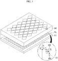
- FIG. 1 is a perspective view illustrating an organic light-emitting diode display device having a touch sensor according to the present disclosure.
- the organic light-emitting diode display device having a touch sensor illustrated in FIG. 1 senses the presence or absence of a touch and a touch position by sensing a variation in mutual capacitance Cm (touch sensor) in response to a user touch via touch electrodes 152e and 154e illustrated in FIG. 2 for a touch period. Then, the organic light-emitting diode display device having a touch sensor illustrated in FIG. 1 displays an image via unit pixels each including a light-emitting element 120. Each unit pixel may include red (R), green (G), and blue (B) subpixels PXL, or may include red (R), green (G), blue (B), and white (W) subpixels PXL.
- the organic light-emitting diode display device illustrated in FIG. 1 includes a plurality of subpixels PXL arranged in a matrix form on a substrate 111 formed, e.g., of a plastic or glass material, an encapsulation unit 140 disposed on the subpixels PXL, and a mutual capacitance array Cm disposed on the encapsulation unit 140.
- Each of the subpixels PXL includes a pixel drive circuit and the light-emitting element 120 connected to the pixel drive circuit.
- the pixel drive circuit includes a switching transistor T1, a driving thin-film transistor T2, and a storage capacitor Cst. Meanwhile, in the present disclosure, a structure in which the pixel drive circuit includes two transistors T and one capacitor C has been described by way of example, but the present disclosure is not limited thereto. That is, a pixel drive circuit having a 3T1C structure or 3T2C structure in which three or more transistors T and one or more capacitors C are provided may be used.
- the switching transistor T1 is turned on when a scan pulse is supplied to a scan line SL, and supplies a data signal supplied to a data line DL to the storage capacitor Cst and a gate electrode of the driving thin-film transistor T2.
- the driving thin-film transistor T2 controls current to be supplied from a high-voltage (VDD) supply line to the light-emitting element 120 in response to the data signal supplied to the gate electrode of the driving thin-film transistor T2, thereby adjusting the amount of emission of light from the light-emitting element 120. Then, even if the switching transistor T1 is turned off, the driving thin-film transistor T2 maintains the emission of light of the light-emitting element 120 by supplying a constant amount of current thereto by a voltage charged in the storage capacitor Cst until a data signal of a next frame is supplied.
- VDD high-voltage
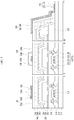
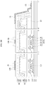
- the driving thin-film transistor T2 or 130 includes a semiconductor layer 134 disposed on a buffer layer 112, a gate electrode 132 overlapping the semiconductor layer 134 with a gate insulation layer 118 therebetween, and source and drain electrodes 136 and 138 formed on an interlayer insulation layer 114 to come into contact with the semiconductor layer 134.
- the semiconductor layer 134 is formed of at least one of an amorphous semiconductor material, a polycrystalline semiconductor material, and an oxide semiconductor material.
- the light-emitting element 120 includes an anode electrode 122, at least one light-emitting stack 124 formed on the anode electrode 122, and a cathode electrode 126 formed on the light-emitting stack 124.
- the anode electrode 122 is electrically connected to the drain electrode 138 of the driving thin-film transistor 130, which is exposed through a pixel contact hole formed in a protective layer 116.
- the light-emitting stack 124 is formed on the anode electrode 122 in a light-emitting area that is defined by a bank 128.
- the light-emitting stack 124 is formed by stacking a hole-related layer, an organic light-emitting layer, and an electron-related layer on the anode electrode 122 in this order or in the reverse order.
- the at least one light-emitting stack 124 may include first and second light-emitting stacks, which face each other with a charge generation layer therebetween.
- the organic light-emitting layer of any one of the first and second light-emitting stacks generates blue light
- the organic light-emitting layer of the other one of the first and second light-emitting stacks generates yellow-green light, whereby white light is generated via the first and second light-emitting stacks. Since the white light generated in the light-emitting stack 124 is incident on a color filter located above or below the light-emitting stack 124, a color image may be realized.
- colored light corresponding to each subpixel may be generated in each light-emitting stack 124 to realize a color image, without a separate color filter.
- the light-emitting stack 124 of the red (R) subpixel may generate red light
- the light-emitting stack 124 of the green (G) subpixel may generate green light
- the light-emitting stack 124 of the blue (B) subpixel may generate blue light.
- the cathode electrode 126 may be formed so as to face the anode electrode 122 with the light-emitting stack 124 therebetween, and is connected to a low-voltage (VSS) supply line.
- VSS low-voltage
- the encapsulation unit 140 prevents external moisture or oxygen from entering the light-emitting element 120, which is vulnerable to the external moisture or oxygen.
- the encapsulation unit 140 includes a plurality of inorganic encapsulation layers 142 and 146 and an organic encapsulation layer 144 disposed between the inorganic encapsulation layers 142 and 146.
- the inorganic encapsulation layer 146 is the uppermost layer.
- the encapsulation unit 140 includes at least two inorganic encapsulation layers 142 and 146 and at least one organic encapsulation layer 144.
- the structure of the encapsulation unit 140 in which the organic encapsulation layer 144 is disposed between first and second inorganic encapsulation layers 142 and 146 will be described by way of example.
- the first inorganic encapsulation layer 142 is formed on the substrate 111, on which the cathode electrode 126 has been formed, so as to be closest to the light-emitting element 120.
- the first inorganic encapsulation layer 142 is formed of an inorganic insulation material that is capable of being deposited at a low temperature, such as silicon nitride (SiN x ), silicon oxide (SiO x ), silicon oxide nitride (SiON), or aluminum oxide (Al 2 O 3 ).
- the first inorganic encapsulation layer 142 is deposited under a low-temperature atmosphere, it is possible to prevent damage to the light-emitting stack 124, which is vulnerable to a high-temperature atmosphere, during the deposition process of the first inorganic encapsulation layer 142.
- the organic encapsulation layer 144 serves to dampen stress between the respective layers due to bending of the organic light-emitting diode display device and to increase planarization performance.
- the organic encapsulation layer 144 is formed on the substrate 111, on which the first inorganic encapsulation layer 142 has been formed, using an organic insulation material, such as an acryl resin, epoxy resin, polyimide, polyethylene, or silicon oxycarbide (SiOC).
- the second inorganic encapsulation layer 146 is formed on the substrate 111, on which the organic encapsulation layer 144 has been formed, so as to cover the upper surface and the side surface of each of the organic encapsulation layer 144 and the first inorganic encapsulation layer 142.
- the second inorganic encapsulation layer 146 minimizes or prevents external moisture or oxygen from entering the first inorganic encapsulation layer 142 and the organic encapsulation layer 144.
- the second inorganic encapsulation layer 146 is formed of an inorganic insulation material, such as silicon nitride (SiN x ), silicon oxide (SiO x ), silicon oxide nitride (SiON), or aluminum oxide (Al 2 O 3 ).
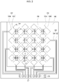
- a touch sensing line 154 and a touch driving line 152 are disposed so as to intersect each other with a touch insulation layer 156 therebetween.
- the term "intersect" is used herein to mean that one element crosses over or overlaps another element, and does not necessarily mean that the two elements contact each other.
- the touch sensing line 154 and touch driving line 152 may intersect each other, but may not physically contact one another since the touch insulation layer 156 is positioned therebetween.
- the touch insulation layer 156 is disposed so as to intersect any one of the touch sensing line 154 and the touch driving line 152 at the intersections of the touch sensing line 154 and the touch driving line 152.
- the mutual capacitance array Cm is formed at the intersections of the touch sensing line 154 and the touch driving line 152.
- the mutual capacitance array Cm serves as a touch sensor by storing charges in response to a touch driving pulse supplied to the touch driving line 152 and discharging the stored charge to the touch sensing line 154.
- the touch driving line 152 includes a plurality of first touch electrodes 152e, and first bridges 152b, which electrically interconnect the first touch electrodes 152e.
- the first touch electrodes 152e are equidistantly spaced apart from each other in the X-direction, which is a first direction, on the second inorganic encapsulation layer 146, which is the uppermost layer of the encapsulation unit 140.
- Each of the first touch electrodes 152e is electrically connected to an adjacent first touch electrode 152e via the first bridge 152b.
- the first touch electrode 152e is electrically connected to a portion of the upper surface and the side surface of the first bridge 152b, which is exposed by the touch insulation layer 156.
- the first touch electrodes 152e are formed of a transparent conductive layer having strong corrosion resistance and acid resistance, such as ITO, IZO, ZnO, IGZO, or ITO/Ag/ITO.
- the first touch electrodes 152e, formed of the transparent conductive layer are configured to completely cover the upper surface and the side surface of the first bridge 152b, which is exposed by the touch insulation layer 156, and are brought into contact with the side surface of the touch insulation layer 156. Thereby, through the use of the first touch electrodes 152e, it is possible to prevent the first bridge 152b from being exposed outwards, and to prevent damage to the first bridge 152b, such as corrosion.
- the first bridge 152b is disposed on the second inorganic encapsulation layer 146 in the same plane as the first touch electrode 152e.
- the length of the first bridge 152b is greater than the line width of the touch insulation layer 156 disposed on the first bridge 152b.
- the first bridge 152b is disposed so as to overlap the bank 128, it is possible to prevent deterioration in the aperture ratio due to the first bridge 152b.
- the first bridge 152b is formed in a single layer or in multiple layers using an opaque conductive layer having good conductivity, such as Al, Ti, Cu, or Mo.
- the first bridge 152b is formed in a triple-layered structure as a stack of Ti/Al/Ti or Mo/Al/Mo.
- the touch sensing line 154 includes a plurality of second touch electrodes 154e, and second bridges 154b, which electrically interconnect the second touch electrodes 154e.
- the second touch electrodes 154e are equidistantly spaced apart from each other in the Y-direction, which is a second direction, on the second inorganic encapsulation layer 146. Each of the second touch electrodes 154e is electrically connected to an adjacent second touch electrode 154e via the second bridge 154b.
- the second bridge 154b extends in the Y-direction from the second touch electrode 154e, and thus is electrically connected to the second touch electrode 154e without a separate contact hole.
- the second bridge 154b is formed on the touch insulation layer 156, which is disposed so as to intersect the first bridge 152b, so as to overlap the touch insulation layer 156.
- the line width of the second bridge 154b is less than the line width of the touch insulation layer 156, which is disposed below the second bridge 154b so as to extend along the second bridge 154b.
- the first and second bridges 152b and 154b are insulated from each other with the touch insulation layer 156 therebetween, which takes the form of an island disposed only at the intersection of the first and second bridges 152b and 154b.
- the second bridge 154b is disposed so as to overlap the bank 128, it is possible to prevent deterioration in the aperture ratio due to the second bridge 154b.
- the second bridge 154b is formed of a transparent conductive layer, such as ITO, IZO, ZnO, IGZO, or ITO/Ag/ITO.
- the touch driving line 152 and the touch sensing line 154 of the present disclosure are connected respectively to touch pads 170 via routing lines 160.
- a routing line 160 extends from a first touch electrode 152e to at least one of the left side and the right side of an active area, and is connected to a touch pad 170.
- another routing line 160 extends from a second touch electrode 154e to at least one of the upper side and the lower side of the active area, and is connected to another touch pad 170.
- the arrangement of the routing lines 160 may be changed in various ways according to design requirements of the display device.
- the routing line 160 is formed between each of the first and second touch electrodes 152e and 154e and the (respective) touch pad 170, and electrically connects each of the first and second touch electrodes 152e and 154e to the touch pad 170.
- the upper portion of the routing line 160 which is electrically connected to each of the first and second touch electrodes 152e and 154e, is disposed above the encapsulation unit 140.
- the lower portion of the routing line 160, which is connected to the touch pad 170, is disposed on (e.g., directly on) any one of the protective layer 116, the interlayer insulation layer 114, the gate insulation layer 118, and the buffer layer 112, which are insulation layers disposed below the light-emitting element 120.
- the side portion of the routing line 160 disposed between the upper portion and the lower portion of the routing line 160, is formed so as to cover the side surface of the second inorganic encapsulation layer 146.
- the side portion of the routing line 160 may be disposed directly on the side surface of the inorganic encapsulation layer 146.
- Each of the routing lines 160 includes a lower routing line 162 and an upper routing line 164 for capping the lower routing line 162.
- the lower routing line 162 is formed by the same mask process as the first bridge 152b using the same material as the first bridge 152b.
- the lower routing line 162 is formed so as to cover and be brought into contact with the side surface of the encapsulation unit 140.
- the upper routing line 164 is formed of the same material as the first and second touch electrodes 152e and 154e and the second bridge 154b.
- the upper routing line 164 extends from each of the first and second touch electrodes 152e and 154e, and is connected to each of the first and second touch electrodes 152e and 154e.
- the upper routing line 164 is formed on the lower routing line 162 so as to cover the side surface and the upper surface of the lower routing line 162, and thus is electrically connected to the lower routing line 162.
- the upper routing line 164 is formed on the lower routing line 162 so as to be directly connected to the lower routing line 162 without a separate contact hole, a connection fault between the upper routing line 162 and the lower routing line 164 may be prevented.
- the routing line 160 which includes the lower routing line 162 and the upper routing line 164, has a multilayered structure, it is possible to reduce the resistance of the routing line 160.
- the routing line 160 has a multilayered structure, even if a break (in other words, a disconnection) occurs in any one of the upper and lower routing lines 162 and 164, the other routing line may perform transmission of the touch driving pulse and the touch signal.
- the touch pads 170 are connected to a signal transmission film on which a touch drive unit (not illustrated) is mounted.
- the touch pads 170 may be disposed in at least one of one side area and the other side area of the substrate 111, together with display pads (not illustrated) connected respectively to at least one of the data line DL, the scan line SL, the low-voltage (VSS) supply line, and the high-voltage (VDD) supply line.
- the touch pads 170 and the display pads may be disposed in different non-active areas. Meanwhile, the arrangement of the touch pads 170 is not limited to the structure of FIG. 2 , and may be changed in various ways according to design requirements of the display device.
- Each of the touch pads 170 includes pad electrodes 172 and 174 formed in multiple layers, and the pad electrode 174 as the uppermost layer is disposed to cover the upper surface and the side surface of the other pad electrode 172 except the pad electrode 174 as the uppermost layer.
- the structure in which the touch pad 170 includes a lower pad electrode 172 and an upper pad electrode 174 will be described by way of example.
- the lower pad electrode 172 is formed by the same mask process as the first bridge 152b using the same material as the first bridge 152b.
- the lower pad electrode 172 extends from the lower routing line 162 on the insulation layer, which is disposed below the light-emitting element 120, and thus, is directly connected to the lower routing line 162.
- the insulation layer disposed below the light-emitting element 120 is any one of the protective layer 116, the interlayer insulation layer 114, the gate insulation layer 118, and the buffer layer 112.
- the lower pad electrode 172 may be disposed directly on the insulation layer.
- the upper pad electrode 174 is formed by the same mask process as the second bridge 154b using the same material as the second bridge 154b.
- the upper pad electrode 174 is formed on the lower pad electrode 172 for capping the lower pad electrode 172, and thus, is directly connected to the lower pad electrode 172 without a separate contact hole.
- each of the first and second touch electrodes 152e and 154e and the second bridge 154b is formed of a transparent conductive layer having strong corrosion resistance and acid resistance, such as ITO, IZO, ZnO, IGZO, or ITO/Ag/ITO.
- a transparent conductive layer having strong corrosion resistance and acid resistance such as ITO, IZO, ZnO, IGZO, or ITO/Ag/ITO.
- each of the upper routing line 164 and the upper pad electrode 174 is formed of a transparent conductive layer having strong corrosion resistance and acid resistance, such as ITO, IZO, ZnO, IGZO, or ITO/Ag/ITO.
- the lower routing line 162 and the lower pad electrode 172 which are formed of an opaque conductive layer, are protected respectively by the upper routing line 164 and the upper pad electrode 174, which are formed of a transparent conductive layer.
- the organic light-emitting diode display device is configured such that the touch electrodes 152e and 154e are disposed on the encapsulation unit 140, which makes a separate attachment process be unnecessary, resulting in a simplified manufacturing process and reduced costs. That is, the touch electrodes 152e and 154e may be formed (e.g., by means of a deposition process) directly on the encapsulation unit without the use of an additional adhesive.
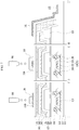
- FIGS. 4A to 6B are plan views and cross-sectional views for explaining a method of manufacturing the organic light-emitting diode display device having the touch sensor illustrated in FIGS. 2 and 3 .
- the first bridge 152b, the lower routing line 162, and the lower pad electrode 172 are formed on the substrate 111 having the switching transistor T1, the driving thin-film transistor T2 or 130, the light-emitting element 120, and the encapsulation unit 140 formed thereon.
- a conductive layer is deposited on the entire surface of the substrate 111, having the switching transistor T1, the driving thin-film transistor T2 or 130, the light-emitting element 120, and the encapsulation unit 140 formed thereon, by a deposition process.
- the conductive layer is patterned by a photolithography process and an etching process using a first mask, whereby the first bridge 152b, the lower routing line 162, and the lower pad electrode 172 are formed.
- each of the first bridge 152b, the lower routing line 162, and the lower pad electrode 172 is formed in a single layer or in multiple layers using an opaque metal having good conductivity, such as Al, Ag, Ti, Cu, Mo, or MoTi.
- each of the first bridge 152b, the lower routing line 162, and the lower pad electrode 172 is formed in a triple-layered structure as a stack of Ti/Al/Ti or Mo/Al/Mo.
- the touch insulation layer 156 is formed on the substrate 111 having the first bridge 152b, the lower routing line 162, and the lower pad electrode 172 formed thereon.
- an inorganic or organic insulation material is deposited on the substrate 111 having the first bridge 152b, the lower routing line 162, and the lower pad electrode 172 formed thereon. Subsequently, the inorganic or organic insulation material is patterned by a photolithography process and an etching process using a second mask, whereby the touch insulation layer 156 is formed.
- the touch insulation layer 156 may be an inorganic layer such as SiN x , SiON, or SiO 2 , or may be an acryl-based, epoxy-based, Parylene-C, Parylene-N, Parylene-F, or siloxane-based organic layer.
- the first and second touch electrodes 152e and 154e, the second bridge 154b, the upper routing line 164, and the upper pad electrode 174 are formed on the substrate 111 having the touch insulation layer 156 formed thereon.
- a transparent conductive layer such as ITO, IZO, ZnO, IGZO, or ITO/Ag/ITO, is disposed on the entire surface of the substrate 111 having the touch insulation layer 156 formed thereon. Subsequently, the transparent conductive layer is patterned by a photolithography process and an etching process using a third mask, whereby the first and second touch electrodes 152e and 154e, the second bridge 154b, the upper routing line 164, and the upper pad electrode 174 are formed.
- a separate protective structure for protecting each of the first and second touch electrodes 152e and 154e, the second bridge 154b, and the upper routing line 164, which are located at the uppermost portion of the touch sensor, is not necessary, a mask process for forming such a protective structure may be omitted.
- the touch sensor since the touch sensor may be formed on the encapsulation unit 140 by the maximum of three mask processes, the structure and the manufacturing process may be simplified, which may increase productivity.
- the touch insulation layer 156 may be formed by a non-mask process. That is, since the resolution of the mutual capacitance array (touch sensor) Cm disposed on the light-emitting element 120 is lower than the resolution of the light-emitting element 120, the touch insulation layer 156 may be formed by an inkjet printing process. Specifically, as illustrated in FIG. 7 , after an organic or inorganic insulation liquid drops onto an area that corresponds to the intersection of the first and second bridges 152b and 154b using an inkjet device 166, the dropped organic or inorganic insulation liquid is cured, whereby the touch insulation layer 156 is formed.
- a mask process for forming the touch insulation layer 156 may be omitted.
- the touch sensor since the touch sensor may be formed on the encapsulation unit 140 by the maximum of two mask processes, the structure and the manufacturing process may be simplified, which may increase productivity.
- the touch insulation layer 156 since the touch insulation layer 156 may be formed by an inkjet printing process, a process of depositing the touch insulation layer 156, a process of baking a photoresist pattern that is used when forming the touch insulation layer 156, and a process of dry-etching the touch insulation layer 156 are not necessary.
- the present disclosure it is possible to prevent the light-emitting stack 124 from being deteriorated by heat generated during the process of depositing the touch insulation layer 156 or the process of baking the photoresist pattern, and it is also possible to prevent the light-emitting stack 124 from being deteriorated by heat and plasma generated during the dry-etching process.
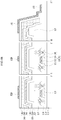
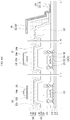
- FIG. 8 is a cross-sectional view illustrating an organic light-emitting diode display device having a touch sensor according to a second embodiment of the present disclosure.
- the organic light-emitting diode display device illustrated in FIG. 8 includes the same constituent elements as those of the organic light-emitting diode display device illustrated in FIG. 3 , except that it further includes color filters 192 disposed between the encapsulation unit 140 and the touch electrodes 152e and 154e. Thus, a detailed description related to the same constituent elements will be omitted below.
- the color filters 192 are formed between each of the touch sensing line 154 and the touch driving line 152 and the light-emitting element 120.
- the distance between each of the touch sensing line 154 and the touch driving line 152 and the light-emitting element 120 is increased by the color filters 192.
- the capacitance of a parasitic capacitor formed between each of the touch sensing line 154 and the touch driving line 152 and the light-emitting element 120 may be minimized, and mutual interaction due to coupling between each of the touch sensing line 154 and the touch driving line 152 and the light-emitting element 120 may be prevented.
- the color filters 192 may prevent a chemical solution (e.g ., developing solution or etching solution) used in the process of manufacturing the touch sensing line 154 and the touch driving line 152, external moisture, and the like from entering the light-emitting stack 124. Thereby, the color filters 192 may prevent damage to the light-emitting stack 124, which is vulnerable to the chemical solution or moisture.
- a chemical solution e.g ., developing solution or etching solution
- the color filters 192 may prevent damage to the light-emitting stack 124, which is vulnerable to the chemical solution or moisture.
- the configuration in which the touch electrodes 152e and 154e are disposed over the color filters 192 has been described by way of example, but the color filters 192 may be disposed over the touch electrodes 152e and 154e. In this case, the touch electrodes 152e and 154e are disposed between the color filters 192 and the encapsulation unit 140.
- a black matrix 194 is disposed between the color filters 192.
- the black matrix 194 serves to separate the respective sub-pixel areas from each other and to prevent optical interference and light leakage between adjacent subpixel areas.
- the black matrix 194 may be formed of a high-resistance black insulation material, or may be formed by stacking at least two colors of color filters among red (R), green (G), and blue (B) color filters 192.
- a touch planarization layer 196 is formed on the substrate 111 having the color filters 192 and the black matrix 194 formed thereon. The substrate 111 having the color filters 192 and the black matrix 194 formed thereon is flattened by the touch planarization layer 196.
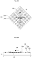
- the first and second touch electrodes 152e and 154e and the first and second bridges 152b and 154b may also be formed to have a mesh shape, as illustrated in FIGS. 9A and 9B . That is, the first and second touch electrodes 152e and 154e and the second bridge 154b may be formed of a transparent conductive layer 1521, such as ITO or IZO, and a mesh metal layer 1522 disposed above or below the transparent conductive layer 1521 and having a mesh shape.
- the touch electrodes 152e and 154e and the second bridge 154b may be formed of only the mesh metal layer 1522 without the transparent conductive layer 1521, or may be formed of the transparent conductive layer 1521 having a mesh shape without the mesh metal layer 1522.
- the mesh metal layer 1522 is formed to have a mesh shape using a highly conductive layer of at least one of Ti, Al, Mo, MoTi, Cu, Ta, and ITO.
- the mesh metal layer 1522 is formed in a triple-layered structure as a stack of Ti/Al/Ti, MoTi/Cu/MoTi, or Ti/Al/Mo.
- the resistance and the capacitance of the first and second touch electrodes 152e and 154e and the second bridge 154b may be reduced, and the RC time constant may be reduced, which may result in increased touch sensitivity.
- the mesh metal layer 1522 of each of the first and second touch electrodes 152e and 154e and the second bridge 154b has a very small line width, it is possible to prevent deterioration in the aperture ratio and transmissivity due to the mesh metal layer 1522.
- the first bridge 152b which is disposed in a plane different from the touch electrodes 152e and 154e, includes a plurality of slits 153, as illustrated in FIGS. 9A and 9B .
- the first bridge 152b having the slits 153 may have a reduced surface area, compared to the first bridge 152b having no slit 153. Thereby, the reflection of external light by the first bridge 152b may be reduced, which may prevent deterioration in visibility. Since the first bridge 152b having the slits 153 overlaps the bank 128, it is possible to prevent deterioration in the aperture ratio by the first bridge 152b formed of an opaque conductive layer.
- a display device includes a touch sensing line and a touch driving line, which intersect each other on an encapsulation unit with a touch insulation layer having an island form therebetween, and the touch insulation layer intersects with any one of the touch sensing line and the touch driving line.
- the structure may be simplified, which may increase reliability.
- a separate protective structure for protecting each of a touch electrode, a bridge, and an upper routing line, which are disposed at the uppermost portion of a touch sensor is not necessary, a mask process for forming such a protective structure may be omitted.
- the touch sensor since the touch sensor may be formed on an encapsulation unit by the maximum of two or three mask processes, the structure and the manufacturing process may be simplified, which may increase productivity. Moreover, by disposing touch electrodes on the encapsulation unit, a separate attachment process may not be necessary, which may further simplify the manufacturing process and reduce costs.
- a display device comprising: a light-emitting element disposed on a substrate; an encapsulation unit disposed on the light-emitting element; a touch sensor disposed on the encapsulation unit and comprising a touch sensing line and a touch driving line; a touch insulation layer having an island shape and disposed between the touch sensing line and the touch driving line at an intersection of the touch sensing line and the touch driving line; and a touch pad connected to the touch sensor and configured with pad electrodes in multiple layers, the pad electrodes including a first pad electrode and a second pad electrode, wherein the second pad electrode is disposed to cover an upper surface and a side surface of the first pad electrode.
- the touch driving line comprises: first touch electrodes arranged in a first direction on the encapsulation unit; and a first bridge configured to interconnect the first touch electrodes, wherein the touch sensing line comprises: second touch electrodes arranged in a second direction intersecting with the first direction; and a second bridge configured to interconnect the second touch electrodes, and wherein the touch insulation layer is disposed below one of the first and second bridges to extend along the corresponding bridge, and intersects with other of the first and second bridges.
- the touch insulation layer is disposed to intersect the first bridge and expose opposite sides of the first bridge, and is disposed to extend along the second bridge with a line width greater than that of the second bridge.
- each of the first touch electrodes is disposed to cover an upper surface and a side surface of the first bridge exposed by the touch insulation layer and to contact a side surface of the touch insulation layer.
- each of the first touch electrodes directly contacts an upper surface and a side surface of the first bridge exposed by the touch insulation layer.
- the first pad electrode is formed of a same material as the first bridge and is disposed on an insulation layer, which is disposed below the light-emitting element; and the second pad electrode is formed of a same material as the second bridge.
- the display device further comprises a routing line disposed between the touch pad and the touch sensor to interconnect the touch pad and the touch sensor, wherein the routing line comprises: a lower routing line formed of a same material as the first bridge; and an upper routing line formed of a same material as the second bridge and disposed to cover a side surface and an upper surface of the lower routing line.
- the upper routing line is formed of the same material as each of the first and second touch electrodes and extends from each of the first and second touch electrodes.
- the lower routing line contacts a side surface of the encapsulation unit.
- At least one of the first bridge and the second bridge comprises at least one slit.
- At least one of the first and second touch electrodes and the first and second bridges is formed to have a mesh shape.
- the display device further comprises a color filter disposed between the encapsulation unit and the touch sensor.
- Various embodiments provide a method of manufacturing a display device, the method comprising: forming a light-emitting element on a substrate; forming an encapsulation unit on the light-emitting element; forming a touch sensor on the encapsulation unit, the touch sensor comprising a touch sensing line and a touch driving line intersecting each other with a touch insulation layer having an island shape therebetween; and forming a touch pad connected to the touch sensor and configured with pad electrodes in multiple layers, wherein the touch insulation layer is disposed between the touch sensing line and the touch driving line at an intersection of the touch sensing line and the touch driving line, and wherein the touch pad includes a first pad electrode and a second pad electrode, and the second pad electrode is disposed to cover an upper surface and a side surface of the first pad electrode.
- the forming the touch sensor comprises: forming a first bridge of the touch driving line on the encapsulation unit; forming the touch insulation layer on the substrate having the first bridge formed thereon; and forming first touch electrodes of the touch driving line on the substrate having the touch insulation layer formed thereon, and a second bridge and second touch electrodes of the touch sensing line, wherein the touch insulation layer is disposed so as to intersect the first bridge and expose opposite sides of the first bridge, and is disposed so as to extend along the second bridge with a line width greater than that of the second bridge.
- the forming the touch insulation layer comprises dropping an organic or inorganic insulation solution onto the first bridge using an inkjet device, and then curing the organic or inorganic insulation solution.
Landscapes
- Engineering & Computer Science (AREA)
- Theoretical Computer Science (AREA)
- General Engineering & Computer Science (AREA)
- Physics & Mathematics (AREA)
- General Physics & Mathematics (AREA)
- Human Computer Interaction (AREA)
- Quality & Reliability (AREA)
- Computer Hardware Design (AREA)
- Electroluminescent Light Sources (AREA)
- Devices For Indicating Variable Information By Combining Individual Elements (AREA)
Abstract
Description
- This application claims the benefit of Korean Patent Application No.
10-2017-0054218, filed April 27, 2017 - The present disclosure relates to a display device and a method of manufacturing the same, and more particularly, to a display device and a method of manufacturing the same that are capable of achieving a simplified manufacturing process and reduced costs.
- A touchscreen is an input device that allows a user to input a command by selecting a content appearing on a screen of a display device or the like with the human hand or an object. That is, the touchscreen converts a contact position that the human hand or the object directly touches into an electrical signal, and receives the content selected at the contact position as an input signal. The touchscreen may substitute for a separate input device, which is connected to the display device and operates, such as a keyboard or a mouse, and thus the use range thereof is gradually expanding.
- Such a touchscreen is generally attached to the front surface of a display panel, such as a liquid crystal display panel or an organic light-emitting diode display panel, via an adhesive in many cases. In this case, since the touchscreen is separately manufactured and attached to the front surface of the display panel, the manufacturing process is complicated and the costs are increased due to addition of such an attachment process.
- Accordingly, the present disclosure is directed to a display device and a method of manufacturing the same that substantially obviate one or more problems due to limitations and disadvantages of the related art.
- The present disclosure has been provided to solve the problems described above, and in various embodiments, the present disclosure provides a display device and a method of manufacturing the same that are capable of achieving a simplified manufacturing process and reduced costs.
- Additional advantages, objects, and features of the disclosure will be set forth in part in the description which follows and in part will become apparent to those having ordinary skill in the art upon examination of the following or may be learned from practice of the disclosure. The objectives and other advantages of the disclosure may be realized and attained by the structure particularly pointed out in the written description and claims hereof as well as the appended drawings.
- To achieve these objects and other advantages and in accordance with the purpose of the disclosure, as embodied and broadly described herein, a display device and a method of manufacturing a display device according to the independent claims are provided. Further embodiments are described in the dependent claims. Various embodiments provide a display device having a touch sensor according to one or more embodiments of the present disclosure includes a touch sensing line and a touch driving line, which are formed on an encapsulation unit and intersect each other with a touch insulation layer interposed therebetween. The touch insulation layer intersects with any one of the touch sensing line and the touch driving line, which may result in the simplified structure. In addition, touch electrodes are disposed on the encapsulation unit, which may make a separate attachment process be unnecessary, resulting in a simplified manufacturing process and reduced costs.
- It is to be understood that both the foregoing general description and the following detailed description of the present disclosure are exemplary and explanatory and are intended to provide further explanation of the disclosure as claimed.
- The accompanying drawings, which are included to provide a further understanding of the disclosure and are incorporated in and constitute a part of this application, illustrate embodiment(s) of the disclosure and together with the description serve to explain the principle of the disclosure. In the drawings:
-
FIG. 1 is a perspective view illustrating an organic light-emitting display device having a touch sensor according to a first embodiment of the present disclosure; -
FIG. 2 is a plan view illustrating the organic light-emitting display device having the touch sensor illustrated inFIG. 1 ; -
FIG. 3 is a cross-sectional view illustrating the organic light-emitting display device having the touch sensor taken along lines "I-I," "II-II," and "III-III" ofFIG. 2 ; -
FIGS. 4A and4B are a plan view and a cross-sectional view, respectively, for explaining a method of manufacturing a first bridge, a lower routing line, and a lower pad electrode illustrated inFIGS. 2 and3 ; -
FIGS. 5A and5B are a plan view and a cross-sectional view, respectively, for explaining a method of manufacturing a touch insulation layer illustrated inFIGS. 2 and3 ; -
FIGS. 6A and6B are a plan view and a cross-sectional view, respectively, for explaining a method of manufacturing a second bridge, first and second touch electrodes, an upper routing line, and an upper pad electrode illustrated inFIGS. 2 and3 ; -
FIG. 7 is a cross-sectional view for explaining another embodiment of the method of manufacturing the touch insulation layer illustrated inFIG. 5B ; -
FIG. 8 is a cross-sectional view illustrating an organic light-emitting display device having a touch sensor according to a second embodiment of the present disclosure; and -
FIGS. 9A and 9B are a plan view and a cross-sectional view, respectively, illustrating another embodiment of first and second touch electrodes and a bridge illustrated inFIG. 3 . - Hereinafter, embodiments according to the present disclosure will be described in detail with reference to the accompanying drawings. Although the embodiments described with reference to the drawings relate mainly to an organic light-emitting diode display device, the disclosure is not restricted to organic light-emitting diode display devices.
-
FIG. 1 is a perspective view illustrating an organic light-emitting diode display device having a touch sensor according to the present disclosure. - The organic light-emitting diode display device having a touch sensor illustrated in
FIG. 1 senses the presence or absence of a touch and a touch position by sensing a variation in mutual capacitance Cm (touch sensor) in response to a user touch viatouch electrodes FIG. 2 for a touch period. Then, the organic light-emitting diode display device having a touch sensor illustrated inFIG. 1 displays an image via unit pixels each including a light-emitting element 120. Each unit pixel may include red (R), green (G), and blue (B) subpixels PXL, or may include red (R), green (G), blue (B), and white (W) subpixels PXL. - To this end, the organic light-emitting diode display device illustrated in
FIG. 1 includes a plurality of subpixels PXL arranged in a matrix form on asubstrate 111 formed, e.g., of a plastic or glass material, anencapsulation unit 140 disposed on the subpixels PXL, and a mutual capacitance array Cm disposed on theencapsulation unit 140. - Each of the subpixels PXL includes a pixel drive circuit and the light-emitting
element 120 connected to the pixel drive circuit. - The pixel drive circuit includes a switching transistor T1, a driving thin-film transistor T2, and a storage capacitor Cst. Meanwhile, in the present disclosure, a structure in which the pixel drive circuit includes two transistors T and one capacitor C has been described by way of example, but the present disclosure is not limited thereto. That is, a pixel drive circuit having a 3T1C structure or 3T2C structure in which three or more transistors T and one or more capacitors C are provided may be used.
- The switching transistor T1 is turned on when a scan pulse is supplied to a scan line SL, and supplies a data signal supplied to a data line DL to the storage capacitor Cst and a gate electrode of the driving thin-film transistor T2.
- The driving thin-film transistor T2 controls current to be supplied from a high-voltage (VDD) supply line to the light-emitting
element 120 in response to the data signal supplied to the gate electrode of the driving thin-film transistor T2, thereby adjusting the amount of emission of light from the light-emitting element 120. Then, even if the switching transistor T1 is turned off, the driving thin-film transistor T2 maintains the emission of light of the light-emittingelement 120 by supplying a constant amount of current thereto by a voltage charged in the storage capacitor Cst until a data signal of a next frame is supplied. - The driving thin-film transistor T2 or 130, as illustrated in
FIG. 3 , includes asemiconductor layer 134 disposed on abuffer layer 112, agate electrode 132 overlapping thesemiconductor layer 134 with agate insulation layer 118 therebetween, and source anddrain electrodes interlayer insulation layer 114 to come into contact with thesemiconductor layer 134. Here, thesemiconductor layer 134 is formed of at least one of an amorphous semiconductor material, a polycrystalline semiconductor material, and an oxide semiconductor material. - The light-emitting
element 120 includes ananode electrode 122, at least one light-emitting stack 124 formed on theanode electrode 122, and acathode electrode 126 formed on the light-emitting stack 124. - The
anode electrode 122 is electrically connected to thedrain electrode 138 of the driving thin-film transistor 130, which is exposed through a pixel contact hole formed in aprotective layer 116. - The light-
emitting stack 124 is formed on theanode electrode 122 in a light-emitting area that is defined by abank 128. The light-emitting stack 124 is formed by stacking a hole-related layer, an organic light-emitting layer, and an electron-related layer on theanode electrode 122 in this order or in the reverse order. In addition, the at least one light-emitting stack 124 may include first and second light-emitting stacks, which face each other with a charge generation layer therebetween. In this case, the organic light-emitting layer of any one of the first and second light-emitting stacks generates blue light, and the organic light-emitting layer of the other one of the first and second light-emitting stacks generates yellow-green light, whereby white light is generated via the first and second light-emitting stacks. Since the white light generated in the light-emitting stack 124 is incident on a color filter located above or below the light-emitting stack 124, a color image may be realized. In addition, colored light corresponding to each subpixel may be generated in each light-emitting stack 124 to realize a color image, without a separate color filter. That is, the light-emitting stack 124 of the red (R) subpixel may generate red light, the light-emitting stack 124 of the green (G) subpixel may generate green light, and the light-emitting stack 124 of the blue (B) subpixel may generate blue light. - The
cathode electrode 126 may be formed so as to face theanode electrode 122 with the light-emitting stack 124 therebetween, and is connected to a low-voltage (VSS) supply line. - The
encapsulation unit 140 prevents external moisture or oxygen from entering the light-emittingelement 120, which is vulnerable to the external moisture or oxygen. To this end, theencapsulation unit 140 includes a plurality of inorganic encapsulation layers 142 and 146 and anorganic encapsulation layer 144 disposed between the inorganic encapsulation layers 142 and 146. Theinorganic encapsulation layer 146 is the uppermost layer. Here, theencapsulation unit 140 includes at least two inorganic encapsulation layers 142 and 146 and at least oneorganic encapsulation layer 144. In the present disclosure, the structure of theencapsulation unit 140 in which theorganic encapsulation layer 144 is disposed between first and second inorganic encapsulation layers 142 and 146 will be described by way of example. - The first
inorganic encapsulation layer 142 is formed on thesubstrate 111, on which thecathode electrode 126 has been formed, so as to be closest to the light-emittingelement 120. The firstinorganic encapsulation layer 142 is formed of an inorganic insulation material that is capable of being deposited at a low temperature, such as silicon nitride (SiNx), silicon oxide (SiOx), silicon oxide nitride (SiON), or aluminum oxide (Al2O3). Thus, since the firstinorganic encapsulation layer 142 is deposited under a low-temperature atmosphere, it is possible to prevent damage to the light-emittingstack 124, which is vulnerable to a high-temperature atmosphere, during the deposition process of the firstinorganic encapsulation layer 142. - The
organic encapsulation layer 144 serves to dampen stress between the respective layers due to bending of the organic light-emitting diode display device and to increase planarization performance. Theorganic encapsulation layer 144 is formed on thesubstrate 111, on which the firstinorganic encapsulation layer 142 has been formed, using an organic insulation material, such as an acryl resin, epoxy resin, polyimide, polyethylene, or silicon oxycarbide (SiOC). - The second
inorganic encapsulation layer 146 is formed on thesubstrate 111, on which theorganic encapsulation layer 144 has been formed, so as to cover the upper surface and the side surface of each of theorganic encapsulation layer 144 and the firstinorganic encapsulation layer 142. Thus, the secondinorganic encapsulation layer 146 minimizes or prevents external moisture or oxygen from entering the firstinorganic encapsulation layer 142 and theorganic encapsulation layer 144. The secondinorganic encapsulation layer 146 is formed of an inorganic insulation material, such as silicon nitride (SiNx), silicon oxide (SiOx), silicon oxide nitride (SiON), or aluminum oxide (Al2O3). - On the
encapsulation unit 140 described above, atouch sensing line 154 and atouch driving line 152 are disposed so as to intersect each other with atouch insulation layer 156 therebetween. The term "intersect" is used herein to mean that one element crosses over or overlaps another element, and does not necessarily mean that the two elements contact each other. For example, thetouch sensing line 154 and touch drivingline 152 may intersect each other, but may not physically contact one another since thetouch insulation layer 156 is positioned therebetween. Here, thetouch insulation layer 156 is disposed so as to intersect any one of thetouch sensing line 154 and thetouch driving line 152 at the intersections of thetouch sensing line 154 and thetouch driving line 152. The mutual capacitance array Cm is formed at the intersections of thetouch sensing line 154 and thetouch driving line 152. Thus, the mutual capacitance array Cm serves as a touch sensor by storing charges in response to a touch driving pulse supplied to thetouch driving line 152 and discharging the stored charge to thetouch sensing line 154. - The
touch driving line 152 includes a plurality offirst touch electrodes 152e, andfirst bridges 152b, which electrically interconnect thefirst touch electrodes 152e. - The
first touch electrodes 152e are equidistantly spaced apart from each other in the X-direction, which is a first direction, on the secondinorganic encapsulation layer 146, which is the uppermost layer of theencapsulation unit 140. Each of thefirst touch electrodes 152e is electrically connected to an adjacentfirst touch electrode 152e via thefirst bridge 152b. Here, thefirst touch electrode 152e is electrically connected to a portion of the upper surface and the side surface of thefirst bridge 152b, which is exposed by thetouch insulation layer 156. - The
first touch electrodes 152e are formed of a transparent conductive layer having strong corrosion resistance and acid resistance, such as ITO, IZO, ZnO, IGZO, or ITO/Ag/ITO. Thefirst touch electrodes 152e, formed of the transparent conductive layer, are configured to completely cover the upper surface and the side surface of thefirst bridge 152b, which is exposed by thetouch insulation layer 156, and are brought into contact with the side surface of thetouch insulation layer 156. Thereby, through the use of thefirst touch electrodes 152e, it is possible to prevent thefirst bridge 152b from being exposed outwards, and to prevent damage to thefirst bridge 152b, such as corrosion. - The
first bridge 152b is disposed on the secondinorganic encapsulation layer 146 in the same plane as thefirst touch electrode 152e. The length of thefirst bridge 152b is greater than the line width of thetouch insulation layer 156 disposed on thefirst bridge 152b. Thereby, since both sides of thefirst bridge 152b are exposed by thetouch insulation layer 156, which intersects with thefirst bridge 152b, thefirst bridge 152b is directly connected to thefirst touch electrode 152e without a separate contact hole. - Since the
first bridge 152b is disposed so as to overlap thebank 128, it is possible to prevent deterioration in the aperture ratio due to thefirst bridge 152b. Thefirst bridge 152b is formed in a single layer or in multiple layers using an opaque conductive layer having good conductivity, such as Al, Ti, Cu, or Mo. For example, thefirst bridge 152b is formed in a triple-layered structure as a stack of Ti/Al/Ti or Mo/Al/Mo. - The
touch sensing line 154 includes a plurality ofsecond touch electrodes 154e, andsecond bridges 154b, which electrically interconnect thesecond touch electrodes 154e. - The
second touch electrodes 154e are equidistantly spaced apart from each other in the Y-direction, which is a second direction, on the secondinorganic encapsulation layer 146. Each of thesecond touch electrodes 154e is electrically connected to an adjacentsecond touch electrode 154e via thesecond bridge 154b. - The
second bridge 154b extends in the Y-direction from thesecond touch electrode 154e, and thus is electrically connected to thesecond touch electrode 154e without a separate contact hole. Thesecond bridge 154b is formed on thetouch insulation layer 156, which is disposed so as to intersect thefirst bridge 152b, so as to overlap thetouch insulation layer 156. Here, the line width of thesecond bridge 154b is less than the line width of thetouch insulation layer 156, which is disposed below thesecond bridge 154b so as to extend along thesecond bridge 154b. Thereby, the first andsecond bridges touch insulation layer 156 therebetween, which takes the form of an island disposed only at the intersection of the first andsecond bridges - Since the
second bridge 154b is disposed so as to overlap thebank 128, it is possible to prevent deterioration in the aperture ratio due to thesecond bridge 154b. In the same manner as the first andsecond touch electrodes second bridge 154b is formed of a transparent conductive layer, such as ITO, IZO, ZnO, IGZO, or ITO/Ag/ITO. - In this way, the
touch driving line 152 and thetouch sensing line 154 of the present disclosure are connected respectively totouch pads 170 via routing lines 160. - A
routing line 160 extends from afirst touch electrode 152e to at least one of the left side and the right side of an active area, and is connected to atouch pad 170. In addition, anotherrouting line 160 extends from asecond touch electrode 154e to at least one of the upper side and the lower side of the active area, and is connected to anothertouch pad 170. The arrangement of therouting lines 160 may be changed in various ways according to design requirements of the display device. - The
routing line 160 is formed between each of the first andsecond touch electrodes touch pad 170, and electrically connects each of the first andsecond touch electrodes touch pad 170. The upper portion of therouting line 160, which is electrically connected to each of the first andsecond touch electrodes encapsulation unit 140. The lower portion of therouting line 160, which is connected to thetouch pad 170, is disposed on (e.g., directly on) any one of theprotective layer 116, theinterlayer insulation layer 114, thegate insulation layer 118, and thebuffer layer 112, which are insulation layers disposed below the light-emittingelement 120. The side portion of therouting line 160, disposed between the upper portion and the lower portion of therouting line 160, is formed so as to cover the side surface of the secondinorganic encapsulation layer 146. The side portion of therouting line 160 may be disposed directly on the side surface of theinorganic encapsulation layer 146. - Each of the
routing lines 160 includes alower routing line 162 and anupper routing line 164 for capping thelower routing line 162. - The
lower routing line 162 is formed by the same mask process as thefirst bridge 152b using the same material as thefirst bridge 152b. Thelower routing line 162 is formed so as to cover and be brought into contact with the side surface of theencapsulation unit 140. - The
upper routing line 164 is formed of the same material as the first andsecond touch electrodes second bridge 154b. Theupper routing line 164 extends from each of the first andsecond touch electrodes second touch electrodes upper routing line 164 is formed on thelower routing line 162 so as to cover the side surface and the upper surface of thelower routing line 162, and thus is electrically connected to thelower routing line 162. In this way, since theupper routing line 164 is formed on thelower routing line 162 so as to be directly connected to thelower routing line 162 without a separate contact hole, a connection fault between theupper routing line 162 and thelower routing line 164 may be prevented. In addition, since therouting line 160, which includes thelower routing line 162 and theupper routing line 164, has a multilayered structure, it is possible to reduce the resistance of therouting line 160. Moreover, since therouting line 160 has a multilayered structure, even if a break (in other words, a disconnection) occurs in any one of the upper andlower routing lines - The
touch pads 170 are connected to a signal transmission film on which a touch drive unit (not illustrated) is mounted. Thetouch pads 170 may be disposed in at least one of one side area and the other side area of thesubstrate 111, together with display pads (not illustrated) connected respectively to at least one of the data line DL, the scan line SL, the low-voltage (VSS) supply line, and the high-voltage (VDD) supply line. Alternatively, thetouch pads 170 and the display pads may be disposed in different non-active areas. Meanwhile, the arrangement of thetouch pads 170 is not limited to the structure ofFIG. 2 , and may be changed in various ways according to design requirements of the display device. - Each of the
touch pads 170 includespad electrodes pad electrode 174 as the uppermost layer is disposed to cover the upper surface and the side surface of theother pad electrode 172 except thepad electrode 174 as the uppermost layer. In the present disclosure, the structure in which thetouch pad 170 includes alower pad electrode 172 and anupper pad electrode 174 will be described by way of example. - The
lower pad electrode 172 is formed by the same mask process as thefirst bridge 152b using the same material as thefirst bridge 152b. Thelower pad electrode 172 extends from thelower routing line 162 on the insulation layer, which is disposed below the light-emittingelement 120, and thus, is directly connected to thelower routing line 162. Here, the insulation layer disposed below the light-emittingelement 120 is any one of theprotective layer 116, theinterlayer insulation layer 114, thegate insulation layer 118, and thebuffer layer 112. Thelower pad electrode 172 may be disposed directly on the insulation layer. - The
upper pad electrode 174 is formed by the same mask process as thesecond bridge 154b using the same material as thesecond bridge 154b. Theupper pad electrode 174 is formed on thelower pad electrode 172 for capping thelower pad electrode 172, and thus, is directly connected to thelower pad electrode 172 without a separate contact hole. - In this way, in the present disclosure, each of the first and
second touch electrodes second bridge 154b is formed of a transparent conductive layer having strong corrosion resistance and acid resistance, such as ITO, IZO, ZnO, IGZO, or ITO/Ag/ITO. Thus, in the present disclosure, since a separate protective structure for protecting each of the first andsecond touch electrodes second bridge 154b, which are located at the uppermost portion of the touch sensor, is not necessary, the simplified structure and the minimized manufacturing process may be achieved. Moreover, in the present disclosure, each of theupper routing line 164 and theupper pad electrode 174 is formed of a transparent conductive layer having strong corrosion resistance and acid resistance, such as ITO, IZO, ZnO, IGZO, or ITO/Ag/ITO. In this case, in the present disclosure, thelower routing line 162 and thelower pad electrode 172, which are formed of an opaque conductive layer, are protected respectively by theupper routing line 164 and theupper pad electrode 174, which are formed of a transparent conductive layer. Thereby, in the present disclosure, since a separate protective structure for protecting each of thelower routing line 162 and thelower pad electrode 172 is not necessary, the simplified structure and the minimized manufacturing process may be achieved. Moreover, unlike a conventional organic light-emitting diode display device configured such that a touchscreen is attached thereto via an adhesive, the organic light-emitting diode display device according to the present disclosure is configured such that thetouch electrodes encapsulation unit 140, which makes a separate attachment process be unnecessary, resulting in a simplified manufacturing process and reduced costs. That is, thetouch electrodes -
FIGS. 4A to 6B are plan views and cross-sectional views for explaining a method of manufacturing the organic light-emitting diode display device having the touch sensor illustrated inFIGS. 2 and3 . - Referring to
FIGS. 4A and4B , thefirst bridge 152b, thelower routing line 162, and thelower pad electrode 172 are formed on thesubstrate 111 having the switching transistor T1, the driving thin-film transistor T2 or 130, the light-emittingelement 120, and theencapsulation unit 140 formed thereon. - Specifically, a conductive layer is deposited on the entire surface of the
substrate 111, having the switching transistor T1, the driving thin-film transistor T2 or 130, the light-emittingelement 120, and theencapsulation unit 140 formed thereon, by a deposition process. Subsequently, the conductive layer is patterned by a photolithography process and an etching process using a first mask, whereby thefirst bridge 152b, thelower routing line 162, and thelower pad electrode 172 are formed. Here, each of thefirst bridge 152b, thelower routing line 162, and thelower pad electrode 172 is formed in a single layer or in multiple layers using an opaque metal having good conductivity, such as Al, Ag, Ti, Cu, Mo, or MoTi. For example, each of thefirst bridge 152b, thelower routing line 162, and thelower pad electrode 172 is formed in a triple-layered structure as a stack of Ti/Al/Ti or Mo/Al/Mo. - Referring to
FIGS. 5A and5B , thetouch insulation layer 156 is formed on thesubstrate 111 having thefirst bridge 152b, thelower routing line 162, and thelower pad electrode 172 formed thereon. - Specifically, an inorganic or organic insulation material is deposited on the
substrate 111 having thefirst bridge 152b, thelower routing line 162, and thelower pad electrode 172 formed thereon. Subsequently, the inorganic or organic insulation material is patterned by a photolithography process and an etching process using a second mask, whereby thetouch insulation layer 156 is formed. Here, thetouch insulation layer 156 may be an inorganic layer such as SiNx, SiON, or SiO2, or may be an acryl-based, epoxy-based, Parylene-C, Parylene-N, Parylene-F, or siloxane-based organic layer. - Referring to
FIGS. 6A and6B , the first andsecond touch electrodes second bridge 154b, theupper routing line 164, and theupper pad electrode 174 are formed on thesubstrate 111 having thetouch insulation layer 156 formed thereon. - Specifically, a transparent conductive layer, such as ITO, IZO, ZnO, IGZO, or ITO/Ag/ITO, is disposed on the entire surface of the
substrate 111 having thetouch insulation layer 156 formed thereon. Subsequently, the transparent conductive layer is patterned by a photolithography process and an etching process using a third mask, whereby the first andsecond touch electrodes second bridge 154b, theupper routing line 164, and theupper pad electrode 174 are formed. - In this way, in the present disclosure, since a separate protective structure for protecting each of the first and
second touch electrodes second bridge 154b, and theupper routing line 164, which are located at the uppermost portion of the touch sensor, is not necessary, a mask process for forming such a protective structure may be omitted. Thereby, in the present disclosure, since the touch sensor may be formed on theencapsulation unit 140 by the maximum of three mask processes, the structure and the manufacturing process may be simplified, which may increase productivity. - Meanwhile, in the present disclosure, a method of forming the
touch insulation layer 156 by a mask process has been described by way of example, but thetouch insulation layer 156 may be formed by a non-mask process. That is, since the resolution of the mutual capacitance array (touch sensor) Cm disposed on the light-emittingelement 120 is lower than the resolution of the light-emittingelement 120, thetouch insulation layer 156 may be formed by an inkjet printing process. Specifically, as illustrated inFIG. 7 , after an organic or inorganic insulation liquid drops onto an area that corresponds to the intersection of the first andsecond bridges inkjet device 166, the dropped organic or inorganic insulation liquid is cured, whereby thetouch insulation layer 156 is formed. In this case, in the present disclosure, a mask process for forming thetouch insulation layer 156 may be omitted. Thereby, in the present disclosure, since the touch sensor may be formed on theencapsulation unit 140 by the maximum of two mask processes, the structure and the manufacturing process may be simplified, which may increase productivity. In addition, in the present disclosure, since thetouch insulation layer 156 may be formed by an inkjet printing process, a process of depositing thetouch insulation layer 156, a process of baking a photoresist pattern that is used when forming thetouch insulation layer 156, and a process of dry-etching thetouch insulation layer 156 are not necessary. Thereby, in the present disclosure, it is possible to prevent the light-emittingstack 124 from being deteriorated by heat generated during the process of depositing thetouch insulation layer 156 or the process of baking the photoresist pattern, and it is also possible to prevent the light-emittingstack 124 from being deteriorated by heat and plasma generated during the dry-etching process. -
FIG. 8 is a cross-sectional view illustrating an organic light-emitting diode display device having a touch sensor according to a second embodiment of the present disclosure. - The organic light-emitting diode display device illustrated in
FIG. 8 includes the same constituent elements as those of the organic light-emitting diode display device illustrated inFIG. 3 , except that it further includescolor filters 192 disposed between theencapsulation unit 140 and thetouch electrodes - The color filters 192 are formed between each of the
touch sensing line 154 and thetouch driving line 152 and the light-emittingelement 120. The distance between each of thetouch sensing line 154 and thetouch driving line 152 and the light-emittingelement 120 is increased by the color filters 192. Thereby, the capacitance of a parasitic capacitor formed between each of thetouch sensing line 154 and thetouch driving line 152 and the light-emittingelement 120 may be minimized, and mutual interaction due to coupling between each of thetouch sensing line 154 and thetouch driving line 152 and the light-emittingelement 120 may be prevented. In addition, thecolor filters 192 may prevent a chemical solution (e.g., developing solution or etching solution) used in the process of manufacturing thetouch sensing line 154 and thetouch driving line 152, external moisture, and the like from entering the light-emittingstack 124. Thereby, thecolor filters 192 may prevent damage to the light-emittingstack 124, which is vulnerable to the chemical solution or moisture. Meanwhile, as illustrated inFIG. 8 , the configuration in which thetouch electrodes color filters 192 has been described by way of example, but thecolor filters 192 may be disposed over thetouch electrodes touch electrodes color filters 192 and theencapsulation unit 140. - A black matrix 194 is disposed between the color filters 192. The black matrix 194 serves to separate the respective sub-pixel areas from each other and to prevent optical interference and light leakage between adjacent subpixel areas. The black matrix 194 may be formed of a high-resistance black insulation material, or may be formed by stacking at least two colors of color filters among red (R), green (G), and blue (B) color filters 192. In addition, a
touch planarization layer 196 is formed on thesubstrate 111 having thecolor filters 192 and the black matrix 194 formed thereon. Thesubstrate 111 having thecolor filters 192 and the black matrix 194 formed thereon is flattened by thetouch planarization layer 196. - Meanwhile, in the present disclosure, although the configuration in which the first and
second touch electrodes second bridges FIG. 2 , has been described by way of example, the first andsecond touch electrodes second bridges FIGS. 9A and 9B . That is, the first andsecond touch electrodes second bridge 154b may be formed of a transparentconductive layer 1521, such as ITO or IZO, and amesh metal layer 1522 disposed above or below the transparentconductive layer 1521 and having a mesh shape. Alternatively, thetouch electrodes second bridge 154b may be formed of only themesh metal layer 1522 without the transparentconductive layer 1521, or may be formed of the transparentconductive layer 1521 having a mesh shape without themesh metal layer 1522. Here, themesh metal layer 1522 is formed to have a mesh shape using a highly conductive layer of at least one of Ti, Al, Mo, MoTi, Cu, Ta, and ITO. For example, themesh metal layer 1522 is formed in a triple-layered structure as a stack of Ti/Al/Ti, MoTi/Cu/MoTi, or Ti/Al/Mo. Thereby, the resistance and the capacitance of the first andsecond touch electrodes second bridge 154b may be reduced, and the RC time constant may be reduced, which may result in increased touch sensitivity. In addition, since themesh metal layer 1522 of each of the first andsecond touch electrodes second bridge 154b has a very small line width, it is possible to prevent deterioration in the aperture ratio and transmissivity due to themesh metal layer 1522. - In addition, the
first bridge 152b, which is disposed in a plane different from thetouch electrodes slits 153, as illustrated inFIGS. 9A and 9B . Thefirst bridge 152b having theslits 153 may have a reduced surface area, compared to thefirst bridge 152b having noslit 153. Thereby, the reflection of external light by thefirst bridge 152b may be reduced, which may prevent deterioration in visibility. Since thefirst bridge 152b having theslits 153 overlaps thebank 128, it is possible to prevent deterioration in the aperture ratio by thefirst bridge 152b formed of an opaque conductive layer. - As is apparent from the above description, a display device according to the present disclosure includes a touch sensing line and a touch driving line, which intersect each other on an encapsulation unit with a touch insulation layer having an island form therebetween, and the touch insulation layer intersects with any one of the touch sensing line and the touch driving line. Thereby, the structure may be simplified, which may increase reliability. In addition, in the present disclosure, a separate protective structure for protecting each of a touch electrode, a bridge, and an upper routing line, which are disposed at the uppermost portion of a touch sensor is not necessary, a mask process for forming such a protective structure may be omitted. As a result, in the present disclosure, since the touch sensor may be formed on an encapsulation unit by the maximum of two or three mask processes, the structure and the manufacturing process may be simplified, which may increase productivity. Moreover, by disposing touch electrodes on the encapsulation unit, a separate attachment process may not be necessary, which may further simplify the manufacturing process and reduce costs.
- Various embodiments provide a display device, comprising: a light-emitting element disposed on a substrate; an encapsulation unit disposed on the light-emitting element; a touch sensor disposed on the encapsulation unit and comprising a touch sensing line and a touch driving line; a touch insulation layer having an island shape and disposed between the touch sensing line and the touch driving line at an intersection of the touch sensing line and the touch driving line; and a touch pad connected to the touch sensor and configured with pad electrodes in multiple layers, the pad electrodes including a first pad electrode and a second pad electrode, wherein the second pad electrode is disposed to cover an upper surface and a side surface of the first pad electrode.
- In one or more embodiments, the touch driving line comprises: first touch electrodes arranged in a first direction on the encapsulation unit; and a first bridge configured to interconnect the first touch electrodes, wherein the touch sensing line comprises: second touch electrodes arranged in a second direction intersecting with the first direction; and a second bridge configured to interconnect the second touch electrodes, and wherein the touch insulation layer is disposed below one of the first and second bridges to extend along the corresponding bridge, and intersects with other of the first and second bridges.
- In one or more embodiments, the touch insulation layer is disposed to intersect the first bridge and expose opposite sides of the first bridge, and is disposed to extend along the second bridge with a line width greater than that of the second bridge.
- In one or more embodiments, each of the first touch electrodes is disposed to cover an upper surface and a side surface of the first bridge exposed by the touch insulation layer and to contact a side surface of the touch insulation layer.
- In one or more embodiments, each of the first touch electrodes directly contacts an upper surface and a side surface of the first bridge exposed by the touch insulation layer.
- In one or more embodiments, the first pad electrode is formed of a same material as the first bridge and is disposed on an insulation layer, which is disposed below the light-emitting element; and the second pad electrode is formed of a same material as the second bridge.
- In one or more embodiments, the display device further comprises a routing line disposed between the touch pad and the touch sensor to interconnect the touch pad and the touch sensor, wherein the routing line comprises: a lower routing line formed of a same material as the first bridge; and an upper routing line formed of a same material as the second bridge and disposed to cover a side surface and an upper surface of the lower routing line.
- In one or more embodiments, the upper routing line is formed of the same material as each of the first and second touch electrodes and extends from each of the first and second touch electrodes.
- In one or more embodiments, the lower routing line contacts a side surface of the encapsulation unit.
- In one or more embodiments, at least one of the first bridge and the second bridge comprises at least one slit.
- In one or more embodiments, at least one of the first and second touch electrodes and the first and second bridges is formed to have a mesh shape.
- In one or more embodiments, the display device further comprises a color filter disposed between the encapsulation unit and the touch sensor.
- Various embodiments provide a method of manufacturing a display device, the method comprising: forming a light-emitting element on a substrate; forming an encapsulation unit on the light-emitting element; forming a touch sensor on the encapsulation unit, the touch sensor comprising a touch sensing line and a touch driving line intersecting each other with a touch insulation layer having an island shape therebetween; and forming a touch pad connected to the touch sensor and configured with pad electrodes in multiple layers, wherein the touch insulation layer is disposed between the touch sensing line and the touch driving line at an intersection of the touch sensing line and the touch driving line, and wherein the touch pad includes a first pad electrode and a second pad electrode, and the second pad electrode is disposed to cover an upper surface and a side surface of the first pad electrode.
- In one or more embodiments, the forming the touch sensor comprises: forming a first bridge of the touch driving line on the encapsulation unit; forming the touch insulation layer on the substrate having the first bridge formed thereon; and forming first touch electrodes of the touch driving line on the substrate having the touch insulation layer formed thereon, and a second bridge and second touch electrodes of the touch sensing line, wherein the touch insulation layer is disposed so as to intersect the first bridge and expose opposite sides of the first bridge, and is disposed so as to extend along the second bridge with a line width greater than that of the second bridge.
- In one or more embodiments, the forming the touch insulation layer comprises dropping an organic or inorganic insulation solution onto the first bridge using an inkjet device, and then curing the organic or inorganic insulation solution.
- Although the embodiments of the present disclosure have been described above in detail with reference to the accompanying drawings, it will be apparent to those skilled in the art that the present disclosure described above is not limited to the embodiments described above, and various substitutions, modifications, and alterations may be devised within the scope of the present disclosure.
- The various embodiments described above can be combined to provide further embodiments. These and other changes can be made to the embodiments in light of the above-detailed description. In general, in the following claims, the terms used should not be construed to limit the claims to the specific embodiments disclosed in the specification and the claims, but should be construed to include all possible embodiments. Accordingly, the claims are not limited by the disclosure.
Claims (15)
- A display device, comprising:a substrate (111);a light-emitting element (120) disposed on the substrate (111);an encapsulation unit (140) disposed on the light-emitting element (120);a touch sensor (Cm) disposed on the encapsulation unit (140) and comprising a touch sensing line (154) and a touch driving line (152);a touch insulation layer (156) having an island shape and disposed between the touch sensing line (154) and the touch driving line (152) at an intersection of the touch sensing line (154) and the touch driving line (152); anda touch pad (170) connected to the touch sensor (Cm) and configured with pad electrodes (172, 174) in multiple layers, the pad electrodes (172, 174) including a first pad electrode (172) and a second pad electrode (174),wherein the second pad electrode (174) is disposed to cover an upper surface and a side surface of the first pad electrode (172).
- The display device according to claim 1, wherein the touch driving line (152) comprises:first touch electrodes (152e) arranged in a first direction on the encapsulation unit (140); anda first bridge (152b) configured to interconnect the first touch electrodes (152e),wherein the touch sensing line (154) comprises:second touch electrodes (154e) arranged in a second direction intersecting with the first direction; anda second bridge (154b) configured to interconnect the second touch electrodes (154e), andwherein the touch insulation layer (156) is disposed below one of the first and second bridges (152b, 154b) to extend along the corresponding bridge, and intersects with other of the first and second bridges (152b, 154b).
- The display device according to claim 2, wherein the touch insulation layer (156) is disposed to intersect the first bridge (152b) and expose opposite sides of the first bridge (152b), and is disposed to extend along the second bridge (154b) with a line width greater than that of the second bridge (154b).
- The display device according to claim 3, wherein each of the first touch electrodes (152e) is disposed to cover an upper surface and a side surface of the first bridge (152b) exposed by the touch insulation layer (156) and to contact a side surface of the touch insulation layer (156).
- The display device according to claim 3, wherein each of the first touch electrodes (152e) directly contacts an upper surface and a side surface of the first bridge (152b) exposed by the touch insulation layer (156).
- The display device according to any one of claims 2 to 5, further comprising an insulation layer, which is disposed below the light-emitting element (120), wherein:the first pad electrode (172) is formed of a same material as the first bridge (152b) and is disposed on the insulation layer; andthe second pad electrode (174) is formed of a same material as the second bridge (154b).
- The display device according to any one of claims 2 to 6, further comprising a routing line (160) disposed between the touch pad (170) and the touch sensor (Cm) to interconnect the touch pad (170) and the touch sensor (Cm),
wherein the routing line (160) comprises:a lower routing line (162) formed of a same material as the first bridge (152b); andan upper routing line (164) formed of a same material as the second bridge (154b) and disposed to cover a side surface and an upper surface of the lower routing line (162). - The display device according to claim 7, wherein the upper routing line (164) is formed of the same material as each of the first and second touch electrodes (152e, 154e) and extends from each of the first and second touch electrodes (152e, 154e).
- The display device according to claim 7 or 8, wherein the lower routing line (162) contacts a side surface of the encapsulation unit (140).
- The display device according to any one of claims 2 to 9, wherein at least one of the first bridge (152b) and the second bridge (154b) comprises at least one slit (153).
- The display device according to any one of claims 2 to 10, wherein at least one of the first and second touch electrodes (152e, 154e) and the first and second bridges (152b, 154b) is formed to have a mesh shape.
- The display device according to any one of claims 1 to 11, further comprising a color filter (192) disposed between the encapsulation unit (140) and the touch sensor (Cm).
- A method of manufacturing a display device, the method comprising:forming a light-emitting element (120) on a substrate (111);forming an encapsulation unit (140) on the light-emitting element (120);forming a touch sensor (Cm) on the encapsulation unit (140), the touch sensor (Cm) comprising a touch sensing line (154) and a touch driving line (152) intersecting each other with a touch insulation layer (156) having an island shape therebetween; andforming a touch pad (170) connected to the touch sensor (Cm) and configured with pad electrodes (172, 174) in multiple layers,wherein the touch insulation layer (156) is disposed between the touch sensing line (154) and the touch driving line (152) at an intersection of the touch sensing line (154) and the touch driving line (152), andwherein the touch pad (170) includes a first pad electrode (172) and a second pad electrode (174), and the second pad electrode (174) is disposed to cover an upper surface and a side surface of the first pad electrode (172).
- The method according to claim 13, wherein the forming the touch sensor (Cm) comprises:forming a first bridge (152b) of the touch driving line (152) on the encapsulation unit (140);forming the touch insulation layer (156) on the substrate (111) having the first bridge (152b) formed thereon; andforming first touch electrodes (152e) of the touch driving line (152) on the substrate (111) having the touch insulation layer (156) formed thereon, and a second bridge (154b) and second touch electrodes (154e) of the touch sensing line (154),wherein the touch insulation layer (156) is disposed so as to intersect the first bridge (152b) and expose opposite sides of the first bridge (152b), and is disposed so as to extend along the second bridge (154b) with a line width greater than that of the second bridge (154b).
- The method according to claim 14, wherein the forming the touch insulation layer (156) comprises dropping an organic or inorganic insulation solution onto the first bridge (152b) using an inkjet device (166), and then curing the organic or inorganic insulation solution.
Applications Claiming Priority (1)
| Application Number | Priority Date | Filing Date | Title |
|---|---|---|---|
| KR1020170054218A KR102330862B1 (en) | 2017-04-27 | 2017-04-27 | Display device and method of fabricating the same |
Publications (2)
| Publication Number | Publication Date |
|---|---|
| EP3396503A1 true EP3396503A1 (en) | 2018-10-31 |
| EP3396503B1 EP3396503B1 (en) | 2022-02-09 |
Family
ID=62063437
Family Applications (1)
| Application Number | Title | Priority Date | Filing Date |
|---|---|---|---|
| EP18169318.5A Active EP3396503B1 (en) | 2017-04-27 | 2018-04-25 | Display device and method of manufacturing the same |
Country Status (5)
| Country | Link |
|---|---|
| US (1) | US10719152B2 (en) |
| EP (1) | EP3396503B1 (en) |
| JP (1) | JP6574286B2 (en) |
| KR (1) | KR102330862B1 (en) |
| CN (1) | CN108958529B (en) |
Cited By (1)
| Publication number | Priority date | Publication date | Assignee | Title |
|---|---|---|---|---|
| CN111158514A (en) * | 2018-11-07 | 2020-05-15 | 三星显示有限公司 | Display device with input sensing unit |
Families Citing this family (18)
| Publication number | Priority date | Publication date | Assignee | Title |
|---|---|---|---|---|
| KR102330862B1 (en) * | 2017-04-27 | 2021-11-24 | 엘지디스플레이 주식회사 | Display device and method of fabricating the same |
| JP6842362B2 (en) * | 2017-05-12 | 2021-03-17 | 株式会社ジャパンディスプレイ | Display device |
| KR102551226B1 (en) * | 2018-07-25 | 2023-07-04 | 삼성디스플레이 주식회사 | Touch member and display device with the same |
| CN108845725B (en) * | 2018-08-21 | 2020-04-10 | 武汉华星光电半导体显示技术有限公司 | Touch substrate, touch screen and electronic device |
| KR102671256B1 (en) * | 2018-11-23 | 2024-06-03 | 엘지디스플레이 주식회사 | Touch panel and touch display device |
| KR102827287B1 (en) * | 2019-01-28 | 2025-07-01 | 삼성디스플레이 주식회사 | Display device and method of manufacturing the same |
| US10817111B1 (en) * | 2019-04-10 | 2020-10-27 | Semiconductor Components Industries, Llc | Methods and apparatus for a capacitive touch sensor |
| KR102819912B1 (en) * | 2019-04-29 | 2025-06-13 | 삼성디스플레이 주식회사 | Input sensing circuit and display device having the same |
| CN110098236A (en) * | 2019-05-14 | 2019-08-06 | 京东方科技集团股份有限公司 | Display base plate and preparation method thereof, display device |
| CN110286789A (en) * | 2019-06-12 | 2019-09-27 | 武汉华星光电半导体显示技术有限公司 | Display panel and display module |
| CN110379939B (en) * | 2019-07-26 | 2022-04-26 | 京东方科技集团股份有限公司 | Display panel, manufacturing method thereof and display device |
| KR102932277B1 (en) * | 2019-12-18 | 2026-02-27 | 삼성디스플레이 주식회사 | Display Device |
| KR102878855B1 (en) * | 2019-12-31 | 2025-10-30 | 엘지디스플레이 주식회사 | Touch display device |
| CN111399688A (en) * | 2020-04-17 | 2020-07-10 | 武汉华星光电半导体显示技术有限公司 | Touch panel and display device |
| KR102909779B1 (en) * | 2020-05-22 | 2026-01-12 | 삼성디스플레이 주식회사 | Display device and manufacturing method of display device |
| KR20220008997A (en) * | 2020-07-14 | 2022-01-24 | 삼성디스플레이 주식회사 | Electronic device |
| CN112269487A (en) * | 2020-09-29 | 2021-01-26 | 合肥维信诺科技有限公司 | a display panel |
| KR20240057845A (en) * | 2022-10-25 | 2024-05-03 | 엘지디스플레이 주식회사 | Display apparatus |
Citations (2)
| Publication number | Priority date | Publication date | Assignee | Title |
|---|---|---|---|---|
| US20120062481A1 (en) * | 2010-09-14 | 2012-03-15 | Samsung Mobile Display Co., Ltd. | Flat panel display with integrated touch screen panel |
| US20160154499A1 (en) * | 2014-11-28 | 2016-06-02 | Samsung Display Co., Ltd. | Display device including touch sensing sensor |
Family Cites Families (37)
| Publication number | Priority date | Publication date | Assignee | Title |
|---|---|---|---|---|
| US6791166B1 (en) * | 2001-04-09 | 2004-09-14 | Amkor Technology, Inc. | Stackable lead frame package using exposed internal lead traces |
| KR101314779B1 (en) * | 2010-08-18 | 2013-10-08 | 엘지디스플레이 주식회사 | Electrostatic capacity type touch screen panel and method of manufacturing the same |
| KR20120032734A (en) * | 2010-09-29 | 2012-04-06 | 삼성모바일디스플레이주식회사 | Touch screen panel and fabricating method thereof |
| TWI447627B (en) * | 2011-03-15 | 2014-08-01 | Mstar Semiconductor Inc | Touch sensing devices |
| KR101363151B1 (en) * | 2011-09-06 | 2014-02-14 | 삼성전자주식회사 | Transparent circuit substrate for touchscreen, method for fabricating the same and touchscreen comprising the same |
| JP5923951B2 (en) * | 2011-12-02 | 2016-05-25 | 大日本印刷株式会社 | Touch panel sensor substrate and method for manufacturing the substrate |
| JP5927915B2 (en) * | 2012-01-11 | 2016-06-01 | 大日本印刷株式会社 | Touch panel sensor substrate and method for manufacturing the substrate |
| KR20130110539A (en) * | 2012-03-29 | 2013-10-10 | 엘지디스플레이 주식회사 | Display device and manufacturing method of the same |
| JP2015164000A (en) * | 2012-06-18 | 2015-09-10 | シャープ株式会社 | Touch panel, display device including touch panel, and method for manufacturing touch panel |
| KR101469487B1 (en) * | 2012-09-18 | 2014-12-05 | 엘지디스플레이 주식회사 | Organic Emitting Display Device |
| KR20140040432A (en) * | 2012-09-26 | 2014-04-03 | 엘지이노텍 주식회사 | Touch panel |
| JP2014085771A (en) * | 2012-10-22 | 2014-05-12 | Toppan Printing Co Ltd | Capacitance type touch panel sensor substrate and method for manufacturing the same and display device |
| JP2014153791A (en) * | 2013-02-06 | 2014-08-25 | Alps Electric Co Ltd | Input device |
| JP2016013958A (en) * | 2013-12-02 | 2016-01-28 | 株式会社半導体エネルギー研究所 | Device and film manufacturing method |
| WO2015098608A1 (en) * | 2013-12-26 | 2015-07-02 | シャープ株式会社 | Touch panel manufacturing method |
| KR102193454B1 (en) * | 2013-12-30 | 2020-12-21 | 엘지디스플레이 주식회사 | Touch Panel and Method of Fabricating the Same |
| KR102240937B1 (en) * | 2014-10-10 | 2021-04-15 | 삼성디스플레이 주식회사 | Display device |
| US9958973B2 (en) * | 2014-10-24 | 2018-05-01 | Lg Display Co., Ltd. | Touch panel and touch panel-integrated organic light emitting display device |
| KR102277379B1 (en) * | 2015-02-25 | 2021-07-14 | 삼성디스플레이 주식회사 | Touch panel and method for manufacturing the same |
| KR102381428B1 (en) * | 2015-03-02 | 2022-04-01 | 삼성디스플레이 주식회사 | Display apparatus |
| JP6498578B2 (en) * | 2015-09-28 | 2019-04-10 | 日本航空電子工業株式会社 | Touch panel |
| KR101739000B1 (en) * | 2015-11-23 | 2017-05-23 | 동우 화인켐 주식회사 | Touch sensor |
| KR101926526B1 (en) * | 2016-06-30 | 2018-12-10 | 엘지디스플레이 주식회사 | Organic light emitting display and fabricating method thereof |
| KR102066099B1 (en) * | 2016-07-29 | 2020-01-14 | 엘지디스플레이 주식회사 | Organic light emitting display and fabricating method thereof |
| KR101908982B1 (en) * | 2016-08-31 | 2018-10-17 | 엘지디스플레이 주식회사 | Organic light emitting display with touch sensor and fabricating method thereof |
| KR101992916B1 (en) * | 2016-09-30 | 2019-06-25 | 엘지디스플레이 주식회사 | Organic light emitting display with touch sensor and fabricating method thereof |
| KR101992915B1 (en) * | 2016-09-30 | 2019-06-25 | 엘지디스플레이 주식회사 | Organic light emitting display with touch sensor and fabricating method thereof |
| JP2018063669A (en) * | 2016-10-14 | 2018-04-19 | 株式会社ジャパンディスプレイ | Display device |
| KR102756220B1 (en) * | 2016-12-28 | 2025-01-17 | 엘지디스플레이 주식회사 | Display device |
| KR102330862B1 (en) * | 2017-04-27 | 2021-11-24 | 엘지디스플레이 주식회사 | Display device and method of fabricating the same |
| KR102354514B1 (en) * | 2017-05-11 | 2022-01-21 | 엘지디스플레이 주식회사 | Display device |
| KR102330864B1 (en) * | 2017-05-12 | 2021-11-24 | 엘지디스플레이 주식회사 | Display device |
| KR102330863B1 (en) * | 2017-05-12 | 2021-11-24 | 엘지디스플레이 주식회사 | Display device |
| KR102363844B1 (en) * | 2017-07-14 | 2022-02-16 | 엘지디스플레이 주식회사 | Display device with a touch sensor |
| KR102546310B1 (en) * | 2018-07-16 | 2023-06-21 | 엘지디스플레이 주식회사 | Display device with touch sensor |
| KR102536348B1 (en) * | 2018-07-19 | 2023-05-24 | 엘지디스플레이 주식회사 | Display device with touch sensor |
| KR102541941B1 (en) * | 2018-07-19 | 2023-06-09 | 엘지디스플레이 주식회사 | Display device with touch sensor |
-
2017
- 2017-04-27 KR KR1020170054218A patent/KR102330862B1/en active Active
-
2018
- 2018-04-25 JP JP2018083630A patent/JP6574286B2/en active Active
- 2018-04-25 CN CN201810377610.1A patent/CN108958529B/en active Active
- 2018-04-25 EP EP18169318.5A patent/EP3396503B1/en active Active
- 2018-04-26 US US15/963,973 patent/US10719152B2/en active Active
Patent Citations (2)
| Publication number | Priority date | Publication date | Assignee | Title |
|---|---|---|---|---|
| US20120062481A1 (en) * | 2010-09-14 | 2012-03-15 | Samsung Mobile Display Co., Ltd. | Flat panel display with integrated touch screen panel |
| US20160154499A1 (en) * | 2014-11-28 | 2016-06-02 | Samsung Display Co., Ltd. | Display device including touch sensing sensor |
Cited By (1)
| Publication number | Priority date | Publication date | Assignee | Title |
|---|---|---|---|---|
| CN111158514A (en) * | 2018-11-07 | 2020-05-15 | 三星显示有限公司 | Display device with input sensing unit |
Also Published As
| Publication number | Publication date |
|---|---|
| JP6574286B2 (en) | 2019-09-11 |
| JP2018190411A (en) | 2018-11-29 |
| KR102330862B1 (en) | 2021-11-24 |
| US20180314372A1 (en) | 2018-11-01 |
| CN108958529A (en) | 2018-12-07 |
| CN108958529B (en) | 2021-06-22 |
| US10719152B2 (en) | 2020-07-21 |
| KR20180120387A (en) | 2018-11-06 |
| EP3396503B1 (en) | 2022-02-09 |
Similar Documents
| Publication | Publication Date | Title |
|---|---|---|
| US11700759B2 (en) | Display device | |
| EP3396503B1 (en) | Display device and method of manufacturing the same | |
| US11620012B2 (en) | Display device | |
| US11301100B2 (en) | Display device | |
| US10490610B2 (en) | Display device | |
| US10763313B2 (en) | Display device | |
| US10802625B2 (en) | Display device having touch sensor and black matrix on the encapsulation unit | |
| US20210397300A1 (en) | Display device | |
| KR20180076688A (en) | Display device | |
| KR20180124613A (en) | Display device | |
| KR102402430B1 (en) | Display device |
Legal Events
| Date | Code | Title | Description |
|---|---|---|---|
| PUAI | Public reference made under article 153(3) epc to a published international application that has entered the european phase |
Free format text: ORIGINAL CODE: 0009012 |
|
| STAA | Information on the status of an ep patent application or granted ep patent |
Free format text: STATUS: REQUEST FOR EXAMINATION WAS MADE |
|
| 17P | Request for examination filed |
Effective date: 20180425 |
|
| AK | Designated contracting states |
Kind code of ref document: A1 Designated state(s): AL AT BE BG CH CY CZ DE DK EE ES FI FR GB GR HR HU IE IS IT LI LT LU LV MC MK MT NL NO PL PT RO RS SE SI SK SM TR |
|
| AX | Request for extension of the european patent |
Extension state: BA ME |
|
| RBV | Designated contracting states (corrected) |
Designated state(s): AL AT BE BG CH CY CZ DE DK EE ES FI FR GB GR HR HU IE IS IT LI LT LU LV MC MK MT NL NO PL PT RO RS SE SI SK SM TR |
|
| GRAP | Despatch of communication of intention to grant a patent |
Free format text: ORIGINAL CODE: EPIDOSNIGR1 |
|
| STAA | Information on the status of an ep patent application or granted ep patent |
Free format text: STATUS: GRANT OF PATENT IS INTENDED |
|
| INTG | Intention to grant announced |
Effective date: 20210706 |
|
| GRAJ | Information related to disapproval of communication of intention to grant by the applicant or resumption of examination proceedings by the epo deleted |
Free format text: ORIGINAL CODE: EPIDOSDIGR1 |
|
| STAA | Information on the status of an ep patent application or granted ep patent |
Free format text: STATUS: REQUEST FOR EXAMINATION WAS MADE |
|
| INTC | Intention to grant announced (deleted) | ||
| GRAS | Grant fee paid |
Free format text: ORIGINAL CODE: EPIDOSNIGR3 |
|
| STAA | Information on the status of an ep patent application or granted ep patent |
Free format text: STATUS: GRANT OF PATENT IS INTENDED |
|
| GRAP | Despatch of communication of intention to grant a patent |
Free format text: ORIGINAL CODE: EPIDOSNIGR1 |
|
| GRAA | (expected) grant |
Free format text: ORIGINAL CODE: 0009210 |
|
| STAA | Information on the status of an ep patent application or granted ep patent |
Free format text: STATUS: THE PATENT HAS BEEN GRANTED |
|
| INTG | Intention to grant announced |
Effective date: 20211220 |
|
| AK | Designated contracting states |
Kind code of ref document: B1 Designated state(s): AL AT BE BG CH CY CZ DE DK EE ES FI FR GB GR HR HU IE IS IT LI LT LU LV MC MK MT NL NO PL PT RO RS SE SI SK SM TR |
|
| REG | Reference to a national code |
Ref country code: GB Ref legal event code: FG4D |
|
| REG | Reference to a national code |
Ref country code: CH Ref legal event code: EP Ref country code: AT Ref legal event code: REF Ref document number: 1467923 Country of ref document: AT Kind code of ref document: T Effective date: 20220215 |
|
| REG | Reference to a national code |
Ref country code: IE Ref legal event code: FG4D |
|
| REG | Reference to a national code |
Ref country code: DE Ref legal event code: R096 Ref document number: 602018030497 Country of ref document: DE |
|
| REG | Reference to a national code |
Ref country code: LT Ref legal event code: MG9D |
|
| REG | Reference to a national code |
Ref country code: NL Ref legal event code: MP Effective date: 20220209 |
|
| REG | Reference to a national code |
Ref country code: AT Ref legal event code: MK05 Ref document number: 1467923 Country of ref document: AT Kind code of ref document: T Effective date: 20220209 |
|
| PG25 | Lapsed in a contracting state [announced via postgrant information from national office to epo] |
Ref country code: SE Free format text: LAPSE BECAUSE OF FAILURE TO SUBMIT A TRANSLATION OF THE DESCRIPTION OR TO PAY THE FEE WITHIN THE PRESCRIBED TIME-LIMIT Effective date: 20220209 Ref country code: RS Free format text: LAPSE BECAUSE OF FAILURE TO SUBMIT A TRANSLATION OF THE DESCRIPTION OR TO PAY THE FEE WITHIN THE PRESCRIBED TIME-LIMIT Effective date: 20220209 Ref country code: PT Free format text: LAPSE BECAUSE OF FAILURE TO SUBMIT A TRANSLATION OF THE DESCRIPTION OR TO PAY THE FEE WITHIN THE PRESCRIBED TIME-LIMIT Effective date: 20220609 Ref country code: NO Free format text: LAPSE BECAUSE OF FAILURE TO SUBMIT A TRANSLATION OF THE DESCRIPTION OR TO PAY THE FEE WITHIN THE PRESCRIBED TIME-LIMIT Effective date: 20220509 Ref country code: NL Free format text: LAPSE BECAUSE OF FAILURE TO SUBMIT A TRANSLATION OF THE DESCRIPTION OR TO PAY THE FEE WITHIN THE PRESCRIBED TIME-LIMIT Effective date: 20220209 Ref country code: LT Free format text: LAPSE BECAUSE OF FAILURE TO SUBMIT A TRANSLATION OF THE DESCRIPTION OR TO PAY THE FEE WITHIN THE PRESCRIBED TIME-LIMIT Effective date: 20220209 Ref country code: HR Free format text: LAPSE BECAUSE OF FAILURE TO SUBMIT A TRANSLATION OF THE DESCRIPTION OR TO PAY THE FEE WITHIN THE PRESCRIBED TIME-LIMIT Effective date: 20220209 Ref country code: ES Free format text: LAPSE BECAUSE OF FAILURE TO SUBMIT A TRANSLATION OF THE DESCRIPTION OR TO PAY THE FEE WITHIN THE PRESCRIBED TIME-LIMIT Effective date: 20220209 Ref country code: BG Free format text: LAPSE BECAUSE OF FAILURE TO SUBMIT A TRANSLATION OF THE DESCRIPTION OR TO PAY THE FEE WITHIN THE PRESCRIBED TIME-LIMIT Effective date: 20220509 |
|
| PG25 | Lapsed in a contracting state [announced via postgrant information from national office to epo] |
Ref country code: PL Free format text: LAPSE BECAUSE OF FAILURE TO SUBMIT A TRANSLATION OF THE DESCRIPTION OR TO PAY THE FEE WITHIN THE PRESCRIBED TIME-LIMIT Effective date: 20220209 Ref country code: LV Free format text: LAPSE BECAUSE OF FAILURE TO SUBMIT A TRANSLATION OF THE DESCRIPTION OR TO PAY THE FEE WITHIN THE PRESCRIBED TIME-LIMIT Effective date: 20220209 Ref country code: GR Free format text: LAPSE BECAUSE OF FAILURE TO SUBMIT A TRANSLATION OF THE DESCRIPTION OR TO PAY THE FEE WITHIN THE PRESCRIBED TIME-LIMIT Effective date: 20220510 Ref country code: FI Free format text: LAPSE BECAUSE OF FAILURE TO SUBMIT A TRANSLATION OF THE DESCRIPTION OR TO PAY THE FEE WITHIN THE PRESCRIBED TIME-LIMIT Effective date: 20220209 Ref country code: AT Free format text: LAPSE BECAUSE OF FAILURE TO SUBMIT A TRANSLATION OF THE DESCRIPTION OR TO PAY THE FEE WITHIN THE PRESCRIBED TIME-LIMIT Effective date: 20220209 |
|
| PG25 | Lapsed in a contracting state [announced via postgrant information from national office to epo] |
Ref country code: IS Free format text: LAPSE BECAUSE OF FAILURE TO SUBMIT A TRANSLATION OF THE DESCRIPTION OR TO PAY THE FEE WITHIN THE PRESCRIBED TIME-LIMIT Effective date: 20220609 |
|
| PG25 | Lapsed in a contracting state [announced via postgrant information from national office to epo] |
Ref country code: SM Free format text: LAPSE BECAUSE OF FAILURE TO SUBMIT A TRANSLATION OF THE DESCRIPTION OR TO PAY THE FEE WITHIN THE PRESCRIBED TIME-LIMIT Effective date: 20220209 Ref country code: SK Free format text: LAPSE BECAUSE OF FAILURE TO SUBMIT A TRANSLATION OF THE DESCRIPTION OR TO PAY THE FEE WITHIN THE PRESCRIBED TIME-LIMIT Effective date: 20220209 Ref country code: RO Free format text: LAPSE BECAUSE OF FAILURE TO SUBMIT A TRANSLATION OF THE DESCRIPTION OR TO PAY THE FEE WITHIN THE PRESCRIBED TIME-LIMIT Effective date: 20220209 Ref country code: EE Free format text: LAPSE BECAUSE OF FAILURE TO SUBMIT A TRANSLATION OF THE DESCRIPTION OR TO PAY THE FEE WITHIN THE PRESCRIBED TIME-LIMIT Effective date: 20220209 Ref country code: DK Free format text: LAPSE BECAUSE OF FAILURE TO SUBMIT A TRANSLATION OF THE DESCRIPTION OR TO PAY THE FEE WITHIN THE PRESCRIBED TIME-LIMIT Effective date: 20220209 Ref country code: CZ Free format text: LAPSE BECAUSE OF FAILURE TO SUBMIT A TRANSLATION OF THE DESCRIPTION OR TO PAY THE FEE WITHIN THE PRESCRIBED TIME-LIMIT Effective date: 20220209 |
|
| REG | Reference to a national code |
Ref country code: DE Ref legal event code: R097 Ref document number: 602018030497 Country of ref document: DE |
|
| PG25 | Lapsed in a contracting state [announced via postgrant information from national office to epo] |
Ref country code: AL Free format text: LAPSE BECAUSE OF FAILURE TO SUBMIT A TRANSLATION OF THE DESCRIPTION OR TO PAY THE FEE WITHIN THE PRESCRIBED TIME-LIMIT Effective date: 20220209 |
|
| REG | Reference to a national code |
Ref country code: CH Ref legal event code: PL |
|
| PLBE | No opposition filed within time limit |
Free format text: ORIGINAL CODE: 0009261 |
|
| STAA | Information on the status of an ep patent application or granted ep patent |
Free format text: STATUS: NO OPPOSITION FILED WITHIN TIME LIMIT |
|
| REG | Reference to a national code |
Ref country code: BE Ref legal event code: MM Effective date: 20220430 |
|
| 26N | No opposition filed |
Effective date: 20221110 |
|
| PG25 | Lapsed in a contracting state [announced via postgrant information from national office to epo] |
Ref country code: MC Free format text: LAPSE BECAUSE OF FAILURE TO SUBMIT A TRANSLATION OF THE DESCRIPTION OR TO PAY THE FEE WITHIN THE PRESCRIBED TIME-LIMIT Effective date: 20220209 Ref country code: LU Free format text: LAPSE BECAUSE OF NON-PAYMENT OF DUE FEES Effective date: 20220425 Ref country code: LI Free format text: LAPSE BECAUSE OF NON-PAYMENT OF DUE FEES Effective date: 20220430 Ref country code: CH Free format text: LAPSE BECAUSE OF NON-PAYMENT OF DUE FEES Effective date: 20220430 |
|
| PG25 | Lapsed in a contracting state [announced via postgrant information from national office to epo] |
Ref country code: SI Free format text: LAPSE BECAUSE OF FAILURE TO SUBMIT A TRANSLATION OF THE DESCRIPTION OR TO PAY THE FEE WITHIN THE PRESCRIBED TIME-LIMIT Effective date: 20220209 Ref country code: BE Free format text: LAPSE BECAUSE OF NON-PAYMENT OF DUE FEES Effective date: 20220430 |
|
| PG25 | Lapsed in a contracting state [announced via postgrant information from national office to epo] |
Ref country code: IE Free format text: LAPSE BECAUSE OF NON-PAYMENT OF DUE FEES Effective date: 20220425 |
|
| PG25 | Lapsed in a contracting state [announced via postgrant information from national office to epo] |
Ref country code: IT Free format text: LAPSE BECAUSE OF FAILURE TO SUBMIT A TRANSLATION OF THE DESCRIPTION OR TO PAY THE FEE WITHIN THE PRESCRIBED TIME-LIMIT Effective date: 20220209 |
|
| PG25 | Lapsed in a contracting state [announced via postgrant information from national office to epo] |
Ref country code: HU Free format text: LAPSE BECAUSE OF FAILURE TO SUBMIT A TRANSLATION OF THE DESCRIPTION OR TO PAY THE FEE WITHIN THE PRESCRIBED TIME-LIMIT; INVALID AB INITIO Effective date: 20180425 |
|
| PG25 | Lapsed in a contracting state [announced via postgrant information from national office to epo] |
Ref country code: MK Free format text: LAPSE BECAUSE OF FAILURE TO SUBMIT A TRANSLATION OF THE DESCRIPTION OR TO PAY THE FEE WITHIN THE PRESCRIBED TIME-LIMIT Effective date: 20220209 Ref country code: CY Free format text: LAPSE BECAUSE OF FAILURE TO SUBMIT A TRANSLATION OF THE DESCRIPTION OR TO PAY THE FEE WITHIN THE PRESCRIBED TIME-LIMIT Effective date: 20220209 |
|
| PG25 | Lapsed in a contracting state [announced via postgrant information from national office to epo] |
Ref country code: MT Free format text: LAPSE BECAUSE OF FAILURE TO SUBMIT A TRANSLATION OF THE DESCRIPTION OR TO PAY THE FEE WITHIN THE PRESCRIBED TIME-LIMIT Effective date: 20220209 |
|
| PGFP | Annual fee paid to national office [announced via postgrant information from national office to epo] |
Ref country code: DE Payment date: 20250220 Year of fee payment: 8 |
|
| PG25 | Lapsed in a contracting state [announced via postgrant information from national office to epo] |
Ref country code: TR Free format text: LAPSE BECAUSE OF FAILURE TO SUBMIT A TRANSLATION OF THE DESCRIPTION OR TO PAY THE FEE WITHIN THE PRESCRIBED TIME-LIMIT Effective date: 20220209 |
|
| PGFP | Annual fee paid to national office [announced via postgrant information from national office to epo] |
Ref country code: GB Payment date: 20260224 Year of fee payment: 9 |
|
| PGFP | Annual fee paid to national office [announced via postgrant information from national office to epo] |
Ref country code: FR Payment date: 20260224 Year of fee payment: 9 |